US6831744B2 - Mirror device, mirror adjustment method, exposure apparatus, exposure method, and semiconductor device manufacturing method - Google Patents
Mirror device, mirror adjustment method, exposure apparatus, exposure method, and semiconductor device manufacturing method Download PDFInfo
- Publication number
- US6831744B2 US6831744B2 US10/389,925 US38992503A US6831744B2 US 6831744 B2 US6831744 B2 US 6831744B2 US 38992503 A US38992503 A US 38992503A US 6831744 B2 US6831744 B2 US 6831744B2
- Authority
- US
- United States
- Prior art keywords
- mirror
- temperature
- exposure
- optical system
- exposure light
- Prior art date
- Legal status (The legal status is an assumption and is not a legal conclusion. Google has not performed a legal analysis and makes no representation as to the accuracy of the status listed.)
- Expired - Fee Related
Links
- 238000004519 manufacturing process Methods 0.000 title claims description 64
- 238000000034 method Methods 0.000 title claims description 39
- 239000004065 semiconductor Substances 0.000 title claims description 37
- 230000003287 optical effect Effects 0.000 claims abstract description 87
- 230000008859 change Effects 0.000 claims description 28
- 238000012423 maintenance Methods 0.000 claims description 18
- 238000005286 illumination Methods 0.000 claims description 17
- 238000012546 transfer Methods 0.000 claims description 13
- 239000000126 substance Substances 0.000 claims description 4
- 238000010438 heat treatment Methods 0.000 claims 8
- 239000002826 coolant Substances 0.000 claims 7
- 235000012431 wafers Nutrition 0.000 description 69
- 239000000498 cooling water Substances 0.000 description 30
- 238000007726 management method Methods 0.000 description 19
- 238000001816 cooling Methods 0.000 description 15
- 239000010408 film Substances 0.000 description 14
- 230000008569 process Effects 0.000 description 14
- 238000012545 processing Methods 0.000 description 12
- 238000013523 data management Methods 0.000 description 11
- 230000009467 reduction Effects 0.000 description 9
- 238000005259 measurement Methods 0.000 description 6
- XUIMIQQOPSSXEZ-UHFFFAOYSA-N Silicon Chemical compound [Si] XUIMIQQOPSSXEZ-UHFFFAOYSA-N 0.000 description 5
- 230000015572 biosynthetic process Effects 0.000 description 5
- 230000006870 function Effects 0.000 description 5
- 229910052710 silicon Inorganic materials 0.000 description 5
- 239000010703 silicon Substances 0.000 description 5
- ZOKXTWBITQBERF-UHFFFAOYSA-N Molybdenum Chemical compound [Mo] ZOKXTWBITQBERF-UHFFFAOYSA-N 0.000 description 4
- 238000001459 lithography Methods 0.000 description 4
- 229910052750 molybdenum Inorganic materials 0.000 description 4
- 239000011733 molybdenum Substances 0.000 description 4
- 230000010355 oscillation Effects 0.000 description 4
- 238000009304 pastoral farming Methods 0.000 description 4
- 230000004044 response Effects 0.000 description 4
- 239000000758 substrate Substances 0.000 description 4
- OKTJSMMVPCPJKN-UHFFFAOYSA-N Carbon Chemical compound [C] OKTJSMMVPCPJKN-UHFFFAOYSA-N 0.000 description 3
- 238000010521 absorption reaction Methods 0.000 description 3
- 229910052799 carbon Inorganic materials 0.000 description 3
- 238000004891 communication Methods 0.000 description 3
- 238000009826 distribution Methods 0.000 description 3
- 238000005530 etching Methods 0.000 description 3
- 238000007689 inspection Methods 0.000 description 3
- 230000004075 alteration Effects 0.000 description 2
- 238000012937 correction Methods 0.000 description 2
- 238000013461 design Methods 0.000 description 2
- 238000001514 detection method Methods 0.000 description 2
- 230000005284 excitation Effects 0.000 description 2
- 239000011521 glass Substances 0.000 description 2
- 238000003384 imaging method Methods 0.000 description 2
- 239000000463 material Substances 0.000 description 2
- 229910052751 metal Inorganic materials 0.000 description 2
- 239000002184 metal Substances 0.000 description 2
- 238000003860 storage Methods 0.000 description 2
- 208000024891 symptom Diseases 0.000 description 2
- 239000013077 target material Substances 0.000 description 2
- 238000012360 testing method Methods 0.000 description 2
- 239000010409 thin film Substances 0.000 description 2
- 239000004215 Carbon black (E152) Substances 0.000 description 1
- 239000006096 absorbing agent Substances 0.000 description 1
- 238000000137 annealing Methods 0.000 description 1
- 239000000872 buffer Substances 0.000 description 1
- 239000003795 chemical substances by application Substances 0.000 description 1
- 238000012790 confirmation Methods 0.000 description 1
- 238000013016 damping Methods 0.000 description 1
- 230000003247 decreasing effect Effects 0.000 description 1
- 230000008021 deposition Effects 0.000 description 1
- 238000005538 encapsulation Methods 0.000 description 1
- 238000000227 grinding Methods 0.000 description 1
- 230000020169 heat generation Effects 0.000 description 1
- 229930195733 hydrocarbon Natural products 0.000 description 1
- 150000002430 hydrocarbons Chemical class 0.000 description 1
- 238000005468 ion implantation Methods 0.000 description 1
- 150000002500 ions Chemical class 0.000 description 1
- 239000004973 liquid crystal related substance Substances 0.000 description 1
- QSHDDOUJBYECFT-UHFFFAOYSA-N mercury Chemical compound [Hg] QSHDDOUJBYECFT-UHFFFAOYSA-N 0.000 description 1
- 238000012544 monitoring process Methods 0.000 description 1
- 230000003647 oxidation Effects 0.000 description 1
- 238000007254 oxidation reaction Methods 0.000 description 1
- 238000012858 packaging process Methods 0.000 description 1
- 230000000737 periodic effect Effects 0.000 description 1
- 238000005498 polishing Methods 0.000 description 1
- HBMJWWWQQXIZIP-UHFFFAOYSA-N silicon carbide Chemical compound [Si+]#[C-] HBMJWWWQQXIZIP-UHFFFAOYSA-N 0.000 description 1
- 229910010271 silicon carbide Inorganic materials 0.000 description 1
- 230000000087 stabilizing effect Effects 0.000 description 1
- 238000013024 troubleshooting Methods 0.000 description 1
- 238000011144 upstream manufacturing Methods 0.000 description 1
- 238000007740 vapor deposition Methods 0.000 description 1
- XLYOFNOQVPJJNP-UHFFFAOYSA-N water Substances O XLYOFNOQVPJJNP-UHFFFAOYSA-N 0.000 description 1
Images


Classifications
-
- G—PHYSICS
- G03—PHOTOGRAPHY; CINEMATOGRAPHY; ANALOGOUS TECHNIQUES USING WAVES OTHER THAN OPTICAL WAVES; ELECTROGRAPHY; HOLOGRAPHY
- G03F—PHOTOMECHANICAL PRODUCTION OF TEXTURED OR PATTERNED SURFACES, e.g. FOR PRINTING, FOR PROCESSING OF SEMICONDUCTOR DEVICES; MATERIALS THEREFOR; ORIGINALS THEREFOR; APPARATUS SPECIALLY ADAPTED THEREFOR
- G03F7/00—Photomechanical, e.g. photolithographic, production of textured or patterned surfaces, e.g. printing surfaces; Materials therefor, e.g. comprising photoresists; Apparatus specially adapted therefor
- G03F7/70—Microphotolithographic exposure; Apparatus therefor
- G03F7/70483—Information management; Active and passive control; Testing; Wafer monitoring, e.g. pattern monitoring
- G03F7/70591—Testing optical components
- G03F7/706—Aberration measurement
-
- G—PHYSICS
- G03—PHOTOGRAPHY; CINEMATOGRAPHY; ANALOGOUS TECHNIQUES USING WAVES OTHER THAN OPTICAL WAVES; ELECTROGRAPHY; HOLOGRAPHY
- G03F—PHOTOMECHANICAL PRODUCTION OF TEXTURED OR PATTERNED SURFACES, e.g. FOR PRINTING, FOR PROCESSING OF SEMICONDUCTOR DEVICES; MATERIALS THEREFOR; ORIGINALS THEREFOR; APPARATUS SPECIALLY ADAPTED THEREFOR
- G03F7/00—Photomechanical, e.g. photolithographic, production of textured or patterned surfaces, e.g. printing surfaces; Materials therefor, e.g. comprising photoresists; Apparatus specially adapted therefor
- G03F7/70—Microphotolithographic exposure; Apparatus therefor
- G03F7/70216—Mask projection systems
- G03F7/70233—Optical aspects of catoptric systems, i.e. comprising only reflective elements, e.g. extreme ultraviolet [EUV] projection systems
-
- G—PHYSICS
- G03—PHOTOGRAPHY; CINEMATOGRAPHY; ANALOGOUS TECHNIQUES USING WAVES OTHER THAN OPTICAL WAVES; ELECTROGRAPHY; HOLOGRAPHY
- G03F—PHOTOMECHANICAL PRODUCTION OF TEXTURED OR PATTERNED SURFACES, e.g. FOR PRINTING, FOR PROCESSING OF SEMICONDUCTOR DEVICES; MATERIALS THEREFOR; ORIGINALS THEREFOR; APPARATUS SPECIALLY ADAPTED THEREFOR
- G03F7/00—Photomechanical, e.g. photolithographic, production of textured or patterned surfaces, e.g. printing surfaces; Materials therefor, e.g. comprising photoresists; Apparatus specially adapted therefor
- G03F7/70—Microphotolithographic exposure; Apparatus therefor
- G03F7/70216—Mask projection systems
- G03F7/70258—Projection system adjustments, e.g. adjustments during exposure or alignment during assembly of projection system
-
- G—PHYSICS
- G03—PHOTOGRAPHY; CINEMATOGRAPHY; ANALOGOUS TECHNIQUES USING WAVES OTHER THAN OPTICAL WAVES; ELECTROGRAPHY; HOLOGRAPHY
- G03F—PHOTOMECHANICAL PRODUCTION OF TEXTURED OR PATTERNED SURFACES, e.g. FOR PRINTING, FOR PROCESSING OF SEMICONDUCTOR DEVICES; MATERIALS THEREFOR; ORIGINALS THEREFOR; APPARATUS SPECIALLY ADAPTED THEREFOR
- G03F7/00—Photomechanical, e.g. photolithographic, production of textured or patterned surfaces, e.g. printing surfaces; Materials therefor, e.g. comprising photoresists; Apparatus specially adapted therefor
- G03F7/70—Microphotolithographic exposure; Apparatus therefor
- G03F7/708—Construction of apparatus, e.g. environment aspects, hygiene aspects or materials
- G03F7/70858—Environment aspects, e.g. pressure of beam-path gas, temperature
- G03F7/70883—Environment aspects, e.g. pressure of beam-path gas, temperature of optical system
- G03F7/70891—Temperature
Definitions
- the present invention relates to a mirror device for transferring a fine circuit pattern, a mirror adjustment method, an exposure apparatus, an exposure method, a semiconductor device manufacturing method using the exposure apparatus, and the like.
- Reduction projection exposure using ultraviolet light has conventionally been performed as a printing (lithography) method of manufacturing a fine semiconductor element such as a semiconductor memory or logic circuit.
- the minimum size capable of transfer by reduction projection exposure is proportional to the wavelength of light used for transfer and inversely proportional to the numerical aperture of the projection optical system.
- the wavelength of light for use is being shortened.
- the wavelength of ultraviolet rays for use is becoming shorter to a mercury-vapor lamp i-line (wavelength: 365 nm), a KrF excimer laser beam (wavelength: 248 nm), and an ArF excimer laser beam (wavelength: 193 nm).
- EUV light extreme ultraviolet light
- a substance greatly absorbs light.
- the use of a lens optical system which utilizes light refraction used for visible light or ultraviolet light is not practical.
- An exposure apparatus using EUV light adopts a reflecting optical system.
- a reticle as a master is a reflecting reticle on which a pattern to be transferred is formed by a light absorber.
- Reflecting optical elements employed in the exposure apparatus using EUV light include a multilayered mirror and a grazing incidence total reflection mirror.
- the real part of the refractive index is slightly smaller than 1 in the EUV region, and total reflection occurs in the grazing incidence state in which EUV light is incident almost parallel to the plane.
- grazing incidence at several degrees from an irradiation plane provides a high reflectance of several ten % or more.
- the degree of freedom in optical design is low, and it is difficult to use the total reflection mirror in the projection optical system.
- An EUV light mirror used for an incident angle almost close to normal incidence is a multilayer mirror obtained by alternately stacking two types of substances having different optical constants.
- Molybdenum and silicon are alternately stacked on the surface of a glass substrate polished into a precise figure.
- the layer thickness is, e.g., 2 nm for the molybdenum layer and about 5 nm for the silicon layer.
- the number of stacked layers is about 20 pairs.
- a value as the sum of the thicknesses of layers of two types of substances will be called a film period.
- the bandwidth is about 0.6 to 1 nm.
- the reflectance of reflected EUV light is about 0.7 at maximum.
- Non-reflected EUV light is absorbed in the multilayer film or substrate, and most of the energy is converted into heat.
- the multilayer mirror exhibits a large optical loss in comparison with a visible light mirror, and the number of mirrors must be minimized.
- a reticle and wafer are simultaneously scanned (scanning exposure) to transfer a pattern in a large area by using only a narrow arcuate region (ring field) spaced apart from the optical axis by a predetermined distance.
- a reduction projection exposure apparatus using EUV light in scanning exposure is mainly constituted by an EUV light source, an illumination optical system, a reflecting reticle, a projection optical system, a reticle stage, a wafer stage, an alignment optical system, and a vacuum system.
- EUV light source e.g., a laser plasma source
- a target material in a vacuum vessel 130 is irradiated with a high-intensity pulse laser beam to generate a high-temperature plasma, and EUV light which is emitted by the plasma and has a wavelength of, e.g., about 13 nm is utilized.
- the target material is a metal thin film, inter gas, droplets, or the like, and is supplied into the vacuum vessel by means such as a gas jet.
- the repetition frequency of the pulse laser is preferably high.
- the pulse laser is generally operated at a repetition frequency of several kHz.
- the illumination optical system is comprised of a plurality of multilayer mirrors or grazing incidence mirrors, an optical integrator, and the like.
- a collection mirror on the first stage collects EUV light almost isotropically emitted from a laser plasma.
- the optical integrator uniformly illuminates a mask at a predetermined numerical aperture.
- An aperture for limiting a region illuminated on the reticle plane to an arcuate figure is formed at a position conjugate to the reticle of the illumination optical system.
- the projection optical system includes a plurality of mirrors. A smaller number of mirrors which constitute the projection optical system provide a higher EUV light utilization efficiency, but make aberration correction difficult.
- the number of mirrors necessary for aberration correction is about four to six.
- the reflecting surface of the mirror has a convex or concave spherical or aspherical figure.
- the numerical aperture NA in this case is about 0.1 to 0.2 (the NA is restricted by a numerical restriction aperture 117 shown by FIGS. 1 and 13 ).
- the mirror is fabricated by grinding and polishing a substrate made of a material with a high rigidity, high hardness, and small thermal expansion coefficient, such as low-expansion-coefficient glass or silicon carbide, into a predetermined reflecting surface figure, and forming multilayer films of molybdenum and silicon on the reflecting surface. If the incident angle is not constant depending on the position within the mirror surface, the reflectance of a multilayer film with a constant film period increases depending on the position, shifting the wavelength of EUV light, as is apparent from Bragg's equation. To prevent this, the film period distribution must be set such that EUV light having the same wavelength is efficiently reflected within the mirror surface.
- the reticle and wafer stages have systems of scanning these stages in synchronism with each other at a velocity ratio proportional to the reduction magnification.
- the scanning direction within the reticle or wafer plane is the X-axis
- an in-plane direction perpendicular to the scanning direction is the Y-axis
- a direction perpendicular to the reticle or wafer plane is the Z-axis.
- a reticle is held by a reticle chuck 116 on the reticle stage.
- the reticle stage has a driving system of moving the reticle stage along the X-axis at a high speed.
- the reticle stage also has fine moving systems in the X-axis direction, Y-axis direction, Z-axis direction, and rotational directions around these axes, and can align a reticle.
- the position and posture of the reticle stage are measured by a laser interferometer, and controlled on the basis of the measurement results.
- a wafer is held on the wafer stage by a wafer chuck 120 .
- the wafer stage has a system of moving the wafer stage long the X-axis at a high speed, similar to the reticle stage.
- the wafer stage also has fine moving systems in the X-axis direction, Y-axis direction, Z-axis direction, and rotational directions around these axes, and can align a wafer.
- the position and posture of the wafer stage are measured by a laser interferometer, and controlled on the basis of the measurement results.
- An alignment detection system 118 measures the positional relationship between the reticle position and the optical axis of the projection optical system, and the positional relationship between the wafer position and the optical axis of the projection optical system.
- the positions and angles of the reticle and wafer stages are set such that a reticle projection image coincides with a predetermined position on a wafer.
- the Z-axis focus position within the wafer plane is measured by a focus position detection system 119 , and the position and angle of the wafer stage are controlled.
- the wafer plane can always keep an imaging position with respect to the projection optical system during exposure.
- the wafer stage moves step by step in the X and Y directions to the next scanning exposure start position.
- the reticle and wafer stages are sync-scanned again in the X direction at a velocity ratio proportional to the reduction magnification of the projection optical system.
- sync scanning operation is repeated (step & scan) while the reduction projection image of a reticle is formed on a wafer.
- the reticle transfer pattern is transferred onto the entire wafer surface.
- the conventional EUV exposure apparatus suffers from the following problems.
- the reflectance of EUV light reflected by the multilayer mirror is about 0.7 at a maximum. Non-reflected light is absorbed in the multilayer film or substrate, and most of the energy is converted into heat.
- the mirror or reticle is irradiated with EUV light, non-reflected light is absorbed in an optical element, generating heat.
- EUV light as exposure light is strongly absorbed in gas.
- EUV light with a wavelength of 13 nm propagates by 1 m through a space filled with air at 10 Pa, about 50% of EUV light is absorbed.
- the space through which EUV light propagates must be maintained at a pressure of at least 10 ⁇ 1 Pa or less, and desirably 10 ⁇ 3 Pa or less.
- the space where the optical element irradiated with EUV light exists must be maintained at a pressure of at least 10 ⁇ 4 Pa or less, and desirably 10 ⁇ 6 Pa or less.
- the EUV optical element cannot be cooled by heat conduction to ambient gas, and must be cooled via a mirror holder or reticle chuck which holds the optical element.
- the mirror and reticle are fixed to the mirror holder and reticle chuck equipped with cooling means of circulating constant-temperature cooling water. Heat generated by absorption of EUV light is externally dissipated from the optical element, suppressing any temperature rise of the optical element.
- the optical element is irradiated with EUV light only during exposure. During the remaining time, e.g., while the wafer stage moves to the next scanning exposure start position, or reticles or wafers are replaced, the optical element is not irradiated with light, and no energy absorption occurs. In other words, energy to the optical element is not temporarily constant and greatly varies with time. It is, therefore, difficult to keep the optical element at a constant temperature by a cooling method of, e.g., circulating constant-temperature cooling water through the mirror holder or reticle chuck which holds the optical element without considering any temporary change of the heat amount absorbed by the optical element. The temperature of the optical element becomes different between the start of exposure and the progress of exposure, and the figure of the reflecting surface inevitably changes.
- the figure is not always kept unchanged even at a constant temperature on the optical element surface due to the temperature distribution inside the optical element and the temperature difference between upper and lower surfaces. Considering deformation factors such as deflection by weight other than the temperature, the optical element figure, i.e., optical characteristic is not always maintained even at a constant temperature on the optical element surface.
- n the number of mirrors which constitute the projection optical system
- ⁇ the wavelength of EUV light
- the temperature rise of an optical element which constitutes the projection optical system causes a surface figure disturbance which exceeds the allowable error.
- the imaging performance of the projection optical system cannot be fully attained, and the resolution and contrast decrease, failing to transfer a fine pattern.
- the present invention has been made to overcome the conventional drawbacks, and has as its object to provide an exposure apparatus capable of stably transferring a fine pattern without any decrease in resolution or contrast upon a change in reflecting surface figure caused by temperature variations of an optical element, a mirror device suitable for the exposure apparatus, and the like.
- the present invention provides a mirror device which constitutes an optical system of an exposure apparatus for transferring a reticle pattern onto a wafer, comprising control means for controlling a reflecting surface figure.
- FIG. 1 is a view for explaining the arrangement of an exposure apparatus according to the present invention
- FIG. 2 is a flow chart for obtaining control of a temperature adjustment system necessary to optimize the mirror figure
- FIG. 3 is a flow chart for obtaining control of the temperature adjustment system necessary to optimize the mirror figure
- FIG. 4 is a graph showing the relationship between the temporary change of the intensity of light incident on a mirror and the temporary change of control of the temperature adjustment system
- FIG. 5 is a graph for explaining an example of measuring a mirror figure error as a function of an output from the temperature adjustment system
- FIG. 6 is a graph for explaining plotted points at which the mirror figure error shown in FIG. 5 is minimized under respective exposure conditions
- FIG. 7 is a graph for explaining plotted points at which the mirror figure error is minimized under respective exposure conditions in accordance with the flow chart of FIG. 3;
- FIG. 8 is a flow chart for explaining a processing flow from acquisition of temperature control data to exposure
- FIG. 9 is a view for explaining the arrangement of a mirror and mirror cooling portion according to the first embodiment of the present invention.
- FIG. 10 is a view for explaining the arrangement of a mirror and mirror cooling portion according to the second embodiment of the present invention.
- FIG. 11 is a view for explaining the arrangement of a mirror and mirror cooling portion according to the third embodiment of the present invention.
- FIG. 12 is a view for explaining an arrangement having a heat pipe in order to reduce vibrations of the mirror cooling portion to the mirror;
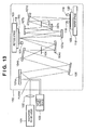
- FIG. 13 is a view for explaining the arrangement of an exposure apparatus using EUV light
- FIG. 14 is a view showing the concept of a semiconductor device production system including an exposure apparatus according to an embodiment of the present invention when viewed from a given angle;
- FIG. 15 is a view showing the concept of the semiconductor device production system including the exposure apparatus according to the embodiment of the present invention when viewed from another angle;
- FIG. 16 is a view showing an example of a user interface in the semiconductor device production system including the exposure apparatus according to the embodiment of the present invention.
- FIG. 17 is a flow chart for explaining the flow of a device manufacturing process by the exposure apparatus according to the embodiment of the present invention.
- FIG. 18 is a flow chart for explaining a wafer process by the exposure apparatus according to the embodiment of the present invention.
- FIG. 13 is a view showing the arrangement of an exposure apparatus using EUV light.
- An exposure apparatus (FIG. 1) according to the first embodiment comprises a timing control system 1 which controls the mirror figure in accordance with incident conditions, i.e., exposure conditions so as to always optimize the mirror figure for exposure in the exposure apparatus using EUV light, and a control data management database 111 .
- the control data management database 111 stores data on the relationship between the incident light intensity, the incident time, and the cooling amount and timing of the mirror figure.
- the timing control system 1 controls a temperature adjustment system (to be described with reference to FIGS. 9 to 12 ) on the basis of data which are acquired in advance and stored in the control data management database 111 , thereby cooling the mirror and controlling the mirror figure.
- a reduction projection exposure apparatus using EUV light is constituted by an exposure light source, an illumination optical system, a reflecting reticle, a projection optical system, a reticle stage, a wafer stage, an alignment optical system, a vacuum system, a timing control system which controls the exposure timing, and a temperature adjustment system which controls the mirror temperature so as to always optimize the mirror figure for exposure.
- the exposure light source is a laser produced by a plasma light source 101 .
- This light source includes a condenser lens 102 and plasma target supply device 103 , and emits EUV light.
- the illumination optical system includes mirrors ( 104 a to 104 c ), an optical integrator 105 , and a view angle restriction aperture 106 which shapes EUV light into an arcuate figure.
- the illumination optical system shapes a laser beam emitted by the plasma light source 101 , and uniformly illuminates a reticle.
- the projection optical system has a plurality of mirrors ( 107 a to 107 d ).
- the projection optical system reduces a reticle pattern formed on a reticle 115 , and transfers the reduced pattern onto a wafer 108 .
- a reticle stage 109 and wafer stage 110 are sync-scanned in accordance with the reduction ratio of the projection optical system.
- the exposure apparatus executes exposure by repeating step & scan, and after exposure to the entire wafer surface is completed, processes the next wafer. Upon the completion of exposure to all wafers, the reticle is replaced, and exposure is repeated again by the same procedures. Exposure light incident conditions such as the interval between the preceding shot and the next shot change depending on each process such as step & scan, wafer replacement, or reticle replacement. To perform stable exposure, the mirror figure must be stabilized by substantially suppressing a change of the minor figure caused by heat generated for every irradiation of exposure light in accordance with exposure light incident conditions. The mirror figure is stabilized by controlling the mirror temperature in accordance with exposure light incident conditions.
- a temperature adjustment systems which controls the temperature of the mirror member, is arranged to enable controlling the mirror temperature. Temperature control conditions for the temperature adjustment system are specified for respective exposure light incident conditions so as to stabilize the mirror figure. In actual exposure, the temperature adjustment system is operated in accordance with the temperature control conditions.
- the exposure apparatus is operated under the same exposure conditions as those of an actual apparatus.
- the mirror is irradiated with light at the same intensity and time interval as those of actual exposure light. While a change of the mirror figure by a temperature change is measured, the relationship between the figure change error and the temperature of the temperature adjustment system is obtained. An optimum control rule of the temperature adjustment system necessary to keep the figure constant is obtained.
- (P′, ⁇ t′) are temperature adjustment system control parameters which minimize the mirror figure error. These parameters are represented by the parameters of incident conditions (P, t 0 ), and determine a controlled variable.
- step S 200 of FIG. 2 the incident light intensity P and exposure timing t 0 are determined in accordance with exposure conditions (upper pulse train in FIG. 4 ).
- a time difference ⁇ t′ is selected (S 210 ). While the temperature control energy P′ of the temperature adjustment system is changed with the fixed time difference ⁇ t′, the mirror figure error is measured by an interferometer (S 220 ).
- a temperature control energy P′ which minimizes the mirror figure error for ⁇ t′ is obtained (S 230 : point at which B- 1 in FIG. 5 becomes minimum in the error distribution). Processing in step S 230 provides a temperature control energy P′ which minimizes the mirror figure error for a predetermined time difference ⁇ t′.
- Data obtained by the above processing steps can be stored and managed as reference table data in the control data management database 111 in FIG. 1 .
- the flow chart of FIG. 2 represents a processing flow of obtaining a condition which optimizes the mirror figure while changing the temperature control energy P′ of the temperature adjustment system with a fixed time difference ⁇ t′.
- the condition decision process is not limited to the above procedures.
- the temperature control energy P′ is first selected (S 310 ), then the mirror figure error is measured while changing the time difference ⁇ t′ (S 320 ), and ⁇ t′ which minimizes the mirror figure error is obtained (S 330 ).
- Data obtained by the above processing steps can be stored and managed as reference table data in the control data management database 111 in FIG. 1 .
- the incident conditions are represented by the parameters (P, t 0 ), and the control parameters of the temperature adjustment system are (P′, ⁇ t′).
- the parameters are not limited to these four parameters.
- temperature adjustment system control parameters which minimize the mirror figure error are obtained while each parameter is changed.
- a larger number of parameters provide a higher mirror figure control precision.
- a series of operations of obtaining the polynomial and change table may be executed for each exposure apparatus or an arbitrary one of a plurality of exposure apparatuses having the same specifications.
- the operation of the temperature adjustment system is determined based on the polynomial or change table.
- the mirror figure becomes constant in an actual arrangement regardless of exposure conditions, and stable exposure can be achieved. That is, stable exposure can be realized by positively changing the mirror temperature so as to keep the mirror figure constant.
- the exposure apparatus incorporates an interferometer to always measure the mirror figure
- the relationship between the mirror figure and the temperature adjustment system is obtained in advance, and stored and managed in the control data management database 111 .
- the mirror figure is measured during exposure, and the temperature adjustment system works based on the data in the control data management database 111 , to keep the mirror figure constant.
- the mirror figure is measured using an interferometer.
- the mirror figure may be estimated from the image point.
- a cooling water channel 5 for adjusting the temperature is formed in a mirror holding portion 4 . Cooling water circulates through the mirror holding portion 4 to control the temperature of a mirror 3 .
- the temperature of cooling water is controlled by a heater 7 on the upstream side of the cooling water channel 5 .
- the power of a heater power supply 6 is controlled via a temperature control system 2 by a signal from the timing control system 1 .
- the relationship between the mirror figure and the heater power is obtained in advance.
- the heater 7 is operated as far as the temperature of the heater 7 can be controlled.
- the temperature of cooling water is changed, and the mirror figure at this temperature is repetitively measured.
- Data on the relationship between the mirror figure and the cooling temperature are collected, and the obtained data are input to the temperature control system 2 .
- the data are always obtained and collected by an interferometer, and are used to keep the mirror figure constant regardless of changes in temperature.
- the operation of the exposure apparatus from acquisition of temperature control data described above to exposure is shown in the flow chart of FIG. 8 .
- the whole operation of the exposure apparatus is executed by the timing control system 1 .
- the timing control system 1 controls the operation timings of the light source, reticle stage 109 , wafer stage 110 , and temperature control system.
- Exposure start and end signals are sent to a pulse laser which is a light source for the exposure (S 801 ).
- the wafer stage 110 receives scanning start and end timings (S 802 ), and the reticle stage 109 receives scanning start and end timings (S 803 ).
- the relationship between the intensity and time of exposure light incident on the mirror is determined when the timing controlled variables of the light source 101 , reticle stage 109 , and wafer stage 110 are input by the timing control system 1 in steps S 801 to S 803 . After the intensity and time of exposure light is determined, the timing control system 1 acquires in step S 804 control data from the control data management database 111 to be sent to the temperature control system 2 .
- the incident light intensity P and incident time t 0 are the intensity and oscillation time of the pulse laser serving as a light source, respectively.
- the temperature control energy P′ of the temperature adjustment system is supplied by the heater 7 inserted in the cooling water channel.
- the time difference ⁇ t′ between the cooling start time and the incidence start time corresponds to the difference between the time at which temperature adjustment of the heater power supply starts and the time at which laser oscilation starts.
- the exposure light intensity and the time are determined from the above mentioned relations.
- the control data management database 111 which is saved in advance as related data between the temperature control energy P′ and the time difference ⁇ t′, is searched.
- the condition (P′, ⁇ t′) which optimizes the mirror figure is determined based on the search.
- the heater 7 is controlled based on the determined condition (P′, ⁇ t′).
- the control data management database 111 contains control data of the temperature control system for stabilizing a figure change caused by heat generation of the mirror upon irradiation of exposure light. Data which minimize the figure error are obtained from the control data management database 111 in accordance with various conditions (S 805 ).
- step S 805 The data obtained in step S 805 are input to the timing control system 1 , and heat timing control is executed via the temperature control system 2 (S 806 ).
- the heater power supply 6 is driven to control the heater 7 , and a predetermined heat amount is applied to cooling water.
- the temperature of the mirror 3 held by the mirror holding portion 4 is stabilized by exchange of the heat amount by cooling water, suppressing any figure change caused by a temperature change.
- step S 807 Scanning exposure starts in step S 807 , and whether the entire wafer surface has been processed is checked (S 808 ). If NO in step S 808 , the wafer stage moves to the next scanning exposure start position (S 811 ). If YES in step S 808 , a wafer replacement signal is sent (NO in S 809 and S 812 ). Exposure start and end timings coincide with the scanning start (S 807 ) and end (S 814 ) of the stage. The wafer is replaced upon the completion of transfer to the entire wafer surface. The reticle (mask) is replaced (NO in S 810 and S 813 ) upon the completion of processing a predetermined number of wafers.
- the timing control system 1 controls the heater power supply 6 via the temperature control system 2 on the basis of heater control data acquired in steps S 804 and S 805 .
- the heater 7 is operated under this control, and after a specific time has elapsed, i.e., the mirror is stabilized in a specific figure, an oscillation start signal is sent to the pulse laser to start exposure. At the same time, scanning start signals are sent to the reticle stage 109 and wafer stage 110 , and transfer of the reticle pattern starts.
- an oscillation end signal is sent to the pulse laser to end exposure.
- the temperature control system 2 adjusts the heater power supply 6 and changes the mirror temperature in accordance with data input to the timing control system 1 in advance so as to keep the mirror figure constant.
- the exposure apparatus repeats step & scan, and after transfer to the entire wafer surface is completed, the wafer is replaced. This timing is also determined based on a signal which is input from the timing control system 1 in advance and sent to the wafer stage. The time necessary to replace wafers is different from the step & scan time interval. Even during this time, the heater power supply is controlled based on data measured in advance, and the mirror figure is kept constant. Upon the completion of transfer to a predetermined number of wafers, the reticle is replaced. Also, at this time, the mirror temperature is so controlled as to keep the mirror figure constant.
- the figure of the mirror 3 is always measured by an interferometer, and the heater power is adjusted in accordance with data input to the timing control system 1 . If the figure changes, the temperature control system 2 adjusts the power on the basis of mirror figure information from the interferometer in accordance with the relationship between the mirror figure and the heater power obtained in advance. Information on the operation timing of the temperature control system 2 and the figure change amount is input to the timing control system 1 to update information of the timing control system. The next exposure can be performed in accordance with the updated information.
- the mirror figure precision increases.
- information of the timing control system 1 is asymptotic to an ideal value.
- the heater power is adjusted in accordance with data input to the timing control system 1 , keeping the figure constant.
- the mirror figure need not be measured by the interferometer.
- the use of data updated by a satisfactory number of times allows an exposure apparatus having the same specifications to perform stable exposure without any figure measurement by the interferometer.
- the mirror figure can be kept constant by changing the cooling water temperature in accordance with the exposure conditions and mirror figure. As a result, stable exposure can be achieved.
- the polynomial and change table are obtained using a heater output parameter as an excitation laser parameter.
- the parameter may be the EUV light intensity observed on the wafer.
- a light intensity sensor is arranged on the wafer in acquiring data for creating a polynomial and change table, and a detected EUV light intensity and timing are used as parameters.
- the EUV light intensity and time detected by the sensor on the wafer respectively correspond to the above-described incident light intensity P and incident time t 0 .
- the polynomial and change table are obtained using a heater output parameter as an excitation laser parameter.
- the parameters may be the cooling water temperature on the downstream side of the heater and the temporary change of this temperature.
- a thermometer is set downstream of the heater, and a detected cooling water temperature and timing are used as parameters.
- the thermometer is electrically connected to the heater power supply, and the heater power is controlled while the cooling water temperature is measured.
- the cooling water temperature and timing detected by the thermometer respectively correspond to the above-described temperature control energy P′ and time difference ⁇ t′ of the temperature adjustment system.
- the first embodiment can provide an exposure apparatus capable of stably transferring a fine pattern without any decrease in resolution or contrast upon a change in reflecting surface figure caused by temperature variations of an optical element.
- the second embodiment is different from the first embodiment in that a system having cooling water for two systems ( 10 a and 10 b ) with different water temperatures, and a valve 8 for adjusting the flow rate of cooling water for each of these two systems is adopted as a cooling water temperature adjustment system, as shown in FIG. 10 .
- a timing control system 1 is connected to a temperature control system 2 , and controls the temperature of cooling water for each system.
- the temperature control system 2 controls heater power supplies 6 a and 6 b and heaters 7 a and 7 b which respectively control the temperature of cooling water 10 a for the first system and that of cooling water 10 b for the second system. Further, the temperature control system 2 controls the opening/closing angle of the valve 8 . By controlling the opening/closing angle of the valve 8 , cooling water flowing through the first system and cooling water flowing through the second system can be controlled at a predetermined flow rate ratio. The temperature can be quickly switched based on the flow rate ratio.
- Cooling water controlled to a predetermined flow rate ratio under the control of the valve 8 flows into a cooling water channel 5 and cools the backside of a mirror 3 via a mirror holding portion 4 which holds the mirror 3 .
- valve control timing of the temperature control system 2 is so controlled as to keep the mirror figure constant on the basis of data measured in advance by the timing control system 1 .
- the cooling temperature can be quickly switched, and a change in reflecting surface figure caused by temperature variations of an optical element can be quickly suppressed.
- the third embodiment is different from the first embodiment in that a Peltier element 9 is interposed as a mirror temperature adjustment system between a mirror 3 and a mirror holding portion 4 , as shown in FIG. 11 .
- the Peltier element 9 is electrically connected to a timing control system 1 via a Peltier element power supply 10 .
- the mirror 3 is heated or cooled in accordance with a current flowing through the Peltier element 9 .
- Cooling water is supplied on the backside (mirror holding portion 4 ) of the Peltier element 9 because the Peltier element 9 dissipates heat absorbed from the mirror 3 .
- a current is supplied from the timing control system 1 to the Peltier element. This timing is so controlled as to keep the mirror figure constant on the basis of data measured in advance by the timing control system 1 , similar to the first embodiment.
- the mediacy of the Peltier element 9 realizes cooling performance with a high response characteristic (follow-up characteristic) which copes with a steep temperature change in response to an instruction from the timing control system 1 .
- FIG. 12 shows this arrangement.
- the heat pipe 12 has a function of conducting heat from the mirror 3 to the cooling portion 4 , and is attached to the mirror 3 directly or via a high-thermal-conductivity metal plate 11 which is attached to the backside of the mirror.
- the heat pipe may be equipped with a damping system such as a bellows, which damps vibrations.
- a plurality of heat pipes 12 or only one heat pipe 12 may be arranged.
- the present invention has been described in terms of an apparatus which starts exposure by oscillation of a pulse laser.
- the present invention is not limited to this, and can also be applied to an exposure apparatus which performs exposure by opening/closing a shutter arranged at a part of the illumination system at the start/end of exposure.
- cooling performance with a high response characteristic (follow-up characteristic) which copes with a steep temperature change can be realized by interposing the Peltier element, in addition to cooling by circulation of cooling water.
- the influence of vibrations by circulation of cooling water can be eliminated.
- a production system for a semiconductor device e.g., a semiconductor chip such a an IC or LSI, a liquid crystal panel, a CCD, a thin-film magnetic head, a micromachine, or the like
- the system performs maintenance services such as trouble shooting, periodic maintenance, and software distribution for manufacturing apparatuses installed in a semiconductor manufacturing factory by utilizing a computer network outside the manufacturing factory.
- FIG. 14 shows the overall system cut out at a given angle.
- reference numeral 1010 denotes an office of a vendor (apparatus supply manufacturer) which provides a semiconductor device manufacturing apparatus.
- the manufacturing apparatus are semiconductor manufacturing apparatuses for performing various processes used in a semiconductor manufacturing factory, such as pre-process apparatuses (e.g., a lithography apparatus including an exposure apparatus, a resist processing apparatus, and an etching apparatus, an annealing apparatus, a film formation apparatus, a planarization apparatus, and the like) and post-process apparatuses (e.g., an assembly apparatus, an inspection apparatus, and the like).
- pre-process apparatuses e.g., a lithography apparatus including an exposure apparatus, a resist processing apparatus, and an etching apparatus, an annealing apparatus, a film formation apparatus, a planarization apparatus, and the like
- post-process apparatuses e.g., an assembly apparatus, an inspection apparatus, and the like.
- the office 1010 comprises a host management system 1080 which provides a maintenance database for the manufacturing apparatus, a plurality of operation terminal computers 1100 , and a LAN (Local Area Network) 1090 which connects the host management system 1080 and computers 1100 to build an intranet.
- the host management system 1080 has a gateway for connecting the LAN 1090 to Internet 1050 serving as an external network of the office, and a security function for limiting external accesses.
- Reference numerals 1020 to 1040 denote manufacturing factories of the semiconductor manufacturer as users of manufacturing apparatuses.
- the manufacturing factories 1020 to 1040 may belong to different manufacturers or the same manufacturer (pre-process factory, post-process factory, and the like).
- Each of the factories 1020 to 1040 is equipped with a plurality of manufacturing apparatuses 1060 , a LAN (Local Area Network) 1110 which connects these apparatuses 1060 to construct an intranet, and a host management system 1070 serving as a monitoring apparatus which monitors the operation status of each manufacturing apparatus 1060 .
- LAN Local Area Network
- the host management system 1070 in each of the factories 1020 to 1040 has a gateway for connecting the LAN 1110 in the factory to the Internet 1050 serving as an external network of the factory.
- Each factory can access the host management system 1080 of the vendor 1010 from the LAN 1110 via the Internet 1050 .
- the security function of the host management system 1080 typically permits only a limited user to access the host management system 1080 .
- the factory can notify the vendor via the Internet 1050 of status information (e.g., the symptom of a manufacturing apparatus in trouble) representing the operation status of each manufacturing apparatus 1060 .
- the vendor can transmit, to the factory, response information (e.g., information designating a remedy against the trouble, or remedy software or data) corresponding to the notification, or maintenance information such as the latest software or help information.
- Data communication between the factories 1020 to 1040 and the vendor 1010 and data communication via the LAN 1110 in each factory typically adopt a communication protocol (TCP/IP) generally used in the Internet.
- TCP/IP communication protocol
- a high-security dedicated network (e.g., ISDN) which inhibits access of a third party can be adopted.
- the host management system is not limited to the one provided by the vendor.
- the user may construct a database and set the database on an external network, and the host management system may authorize access to the database from a plurality of user factories.
- FIG. 15 is a view showing the concept of the overall system of this embodiment that is cut out at a different angle from FIG. 14 .
- a plurality of user factories having manufacturing apparatuses and the management system of the manufacturing apparatus vendor are connected via an external network, and production management of each factory or information about at least one manufacturing apparatus is communicated via the external network.
- a factory having a plurality of manufacturing apparatuses provided by a plurality of vendors and the management systems of the vendors for these manufacturing apparatuses are connected via the external network of the factory, and maintenance information about each manufacturing apparatus is communicated.
- reference numeral 2010 denotes a manufacturing factory of a manufacturing apparatus user (e.g., a semiconductor device manufacturer). Manufacturing apparatuses for performing various processes, e.g., an exposure apparatus 2020 , a resist processing apparatus 2030 , and a film formation apparatus 2040 are installed in the manufacturing line of the factory.
- FIG. 15 shows only one manufacturing factory 2010 , but a plurality of factories are networked in practice.
- the respective apparatuses in the factory are connected to each other by a LAN 2060 to build an intranet, and a host management system 2050 manages the operation of the manufacturing line.
- the offices of vendors e.g., apparatus supply manufacturers
- Such as an exposure apparatus manufacturer 2100 , a resist processing apparatus manufacturer 2200 , and a film formation apparatus manufacturer 2300 comprise host management systems 2110 , 2210 , and 2310 for executing remote maintenance for the supplied apparatuses.
- Each host management system has a maintenance database and a gateway for an external network, as described above.
- the host management system 2050 which manages the apparatuses in the manufacturing factory of the user, and the management systems 2110 , 2210 , and 2310 of the vendors for the respective apparatuses are connected via the Internet or dedicated network serving as an external network 2000 .
- the Internet or dedicated network serving as an external network 2000 .
- Each manufacturing apparatus in the semiconductor manufacturing factory comprises a display, a network interface, and a computer which executes network access software and apparatus operating software that are stored in a storage device.
- the storage device is a built-in memory, hard disk, or network file server.
- the network access software includes a dedicated or general-purpose web browser, and provides a user interface with a window as shown in FIG. 16 on the display.
- the operator who manages manufacturing apparatuses in each factory inputs, into input fields on the windows, pieces of information such as the model of manufacturing apparatus ( 4010 ), serial number ( 4020 ), subject of trouble ( 4030 ), date of occurrence of trouble ( 4040 ), degree of urgency ( 4050 ), symptom ( 4060 ), remedy ( 4070 ), and progress ( 4080 ).
- the pieces of input information are transmitted to the maintenance database via the Internet, and appropriate maintenance information is sent back from the maintenance database and provided on the display.
- the user interface provided by the web browser realizes hyperlink functions ( 4100 to 4120 ), as shown in FIG. 16 . This allows the operator to access more detailed information of each item, download the latest-version software to be used for a manufacturing apparatus from a software library provided by a vendor, and download an operation guide (help information) as a reference for the operator in the factory.
- FIG. 17 shows the flow of the whole manufacturing process of a semiconductor device.
- circuit design a semiconductor device circuit is designed.
- exposure control data creation exposure control data for an exposure apparatus is created on the basis of the designed circuit pattern.
- step 3 wafer formation
- a wafer is formed using a material such as silicon.
- step 4 wafer process
- an actual circuit is formed on the wafer by lithography using a the prepared mask and wafer.
- Step 5 is the step of forming a semiconductor chip by using the wafer formed in step 4 , and includes an assembly process (dicing and bonding) and a packaging process (chip encapsulation).
- step 6 the semiconductor device manufactured in step 5 undergoes inspections such as an operation confirmation test and a durability test.
- the semiconductor device is completed and shipped (step 7 ).
- the pre-process and post-process maybe performed in separate dedicated factories. In this case, each of the factories receives maintenance by the above-described remote maintenance system. Information for production management and apparatus maintenance is communicated between the pre-process factory and the post-process factory via the Internet or dedicated network.
- FIG. 18 shows the detailed flow of the wafer process.
- step 11 oxidation
- step 12 CVD
- step 13 electrode formation
- step 14 ion implantation
- step 15 resist processing
- step 16 exposure
- step 17 developing
- step 18 etching
- the resist is etched except the developed resist image.
- step 19 resist removal
- step 19 resist removal
- steps 19 resist removal
- steps 19 are repeated to form multiple circuit patterns on the wafer.
- a manufacturing apparatus used in each step undergoes maintenance by the remote maintenance system, which prevents trouble in advance. Even if trouble occurs, the manufacturing apparatus can be quickly recovered.
- the semiconductor device productivity can be increased in comparison with the prior art.
- the present invention can easily control a figure change of the mirror (reflecting surface) in accordance with exposure conditions, and realize exposure at a stable precision.
- the present invention can provide an exposure apparatus capable of stably transferring a fine pattern while properly preventing any decrease in resolution or contrast upon a change in reflecting surface figure caused by temperature variations of an optical element, and a semiconductor device manufacturing method using the exposure apparatus.
Landscapes
- General Physics & Mathematics (AREA)
- Physics & Mathematics (AREA)
- Health & Medical Sciences (AREA)
- Toxicology (AREA)
- Engineering & Computer Science (AREA)
- Environmental & Geological Engineering (AREA)
- Epidemiology (AREA)
- Public Health (AREA)
- Atmospheric Sciences (AREA)
- Life Sciences & Earth Sciences (AREA)
- Exposure And Positioning Against Photoresist Photosensitive Materials (AREA)
- Exposure Of Semiconductors, Excluding Electron Or Ion Beam Exposure (AREA)
- Optical Elements Other Than Lenses (AREA)
Applications Claiming Priority (2)
| Application Number | Priority Date | Filing Date | Title |
|---|---|---|---|
| JP2002-078917 | 2002-03-20 | ||
| JP2002078917A JP4006251B2 (ja) | 2002-03-20 | 2002-03-20 | ミラー装置、ミラーの調整方法、露光装置、露光方法及び半導体デバイスの製造方法 |
Publications (2)
| Publication Number | Publication Date |
|---|---|
| US20030179377A1 US20030179377A1 (en) | 2003-09-25 |
| US6831744B2 true US6831744B2 (en) | 2004-12-14 |
Family
ID=28035617
Family Applications (1)
| Application Number | Title | Priority Date | Filing Date |
|---|---|---|---|
| US10/389,925 Expired - Fee Related US6831744B2 (en) | 2002-03-20 | 2003-03-18 | Mirror device, mirror adjustment method, exposure apparatus, exposure method, and semiconductor device manufacturing method |
Country Status (3)
| Country | Link |
|---|---|
| US (1) | US6831744B2 (enExample) |
| EP (1) | EP1353232A3 (enExample) |
| JP (1) | JP4006251B2 (enExample) |
Cited By (7)
| Publication number | Priority date | Publication date | Assignee | Title |
|---|---|---|---|---|
| US20070285638A1 (en) * | 2006-06-07 | 2007-12-13 | Asml Netherlands B.V. | Mirror array for lithography |
| US20080291413A1 (en) * | 2007-05-24 | 2008-11-27 | Asml Netherlands B.V. | Lithographic apparatus having encoder type position sensor system |
| US20090002653A1 (en) * | 2007-05-24 | 2009-01-01 | Asml Netherlands B.V. | Lithographic apparatus having encoder type position sensor system |
| US20090288003A1 (en) * | 2006-05-31 | 2009-11-19 | Marinkovic Sinisa V | Cost effective system and method for monitoring machinery units |
| US20100271679A1 (en) * | 2009-04-23 | 2010-10-28 | Brown David C | Systems and methods of providing improved performance of scanning mirrors coupled to limited rotation motors |
| US20120212719A1 (en) * | 2011-02-17 | 2012-08-23 | Giovanni Bianucci | Thermal management systems, assemblies and methods for grazing incidence collectors for euv lithography |
| US20120281189A1 (en) * | 2011-05-04 | 2012-11-08 | Media Lario S.R.L | Evaporative thermal management of grazing incidence collectors for EUV lithography |
Families Citing this family (19)
| Publication number | Priority date | Publication date | Assignee | Title |
|---|---|---|---|---|
| JP4458333B2 (ja) | 2003-02-13 | 2010-04-28 | キヤノン株式会社 | 露光装置、およびデバイスの製造方法 |
| JP4311711B2 (ja) * | 2003-02-24 | 2009-08-12 | キヤノン株式会社 | 露光装置及びデバイス製造方法 |
| DE10317662A1 (de) * | 2003-04-17 | 2004-11-18 | Carl Zeiss Smt Ag | Projektionsobjektiv, mikrolithographische Projektionsbelichtungsanlage und Verfahren zur Herstellung einer Halbleiterschaltung |
| US7025498B2 (en) * | 2003-05-30 | 2006-04-11 | Asml Holding N.V. | System and method of measuring thermal expansion |
| JP2005175187A (ja) * | 2003-12-11 | 2005-06-30 | Canon Inc | 光学部材、冷却方法、冷却装置、露光装置、デバイス製造方法、及びデバイス |
| JP4903691B2 (ja) * | 2004-05-06 | 2012-03-28 | カール ツァイス レーザー オプティクス ゲーエムベーハー | 熱挙動が改良された光学部品 |
| US7423765B2 (en) * | 2004-07-31 | 2008-09-09 | Carl Zeiss Smt Ag | Optical system of a microlithographic projection exposure apparatus |
| US7423721B2 (en) * | 2004-12-15 | 2008-09-09 | Asml Netherlands B.V. | Lithographic apparatus |
| US7462841B2 (en) | 2005-10-19 | 2008-12-09 | Asml Netherlands B.V. | Lithographic apparatus, device manufacturing method, and use of a radiation collector |
| TWI454859B (zh) * | 2006-03-30 | 2014-10-01 | 尼康股份有限公司 | 移動體裝置、曝光裝置與曝光方法以及元件製造方法 |
| DE102009054869B4 (de) * | 2009-04-09 | 2022-02-17 | Carl Zeiss Smt Gmbh | Spiegel zur Führung eines Strahlungsbündels, Vorrichtungen mit einem derartigen Spiegel sowie Verfahren zur Herstellung mikro- oder nanostrukturierter Bauelemente |
| DE102011004446A1 (de) * | 2011-02-21 | 2012-08-23 | Carl Zeiss Smt Gmbh | Gekühltes optisches Element |
| DE102014203144A1 (de) * | 2014-02-21 | 2015-08-27 | Carl Zeiss Smt Gmbh | Baugruppe eines optischen Systems, insbesondere in einer mikrolithographischen Projektionsbelichtungsanlage |
| SG11201707040PA (en) * | 2015-03-24 | 2017-10-30 | Asml Netherlands Bv | A lithography apparatus and a method of manufacturing a device |
| DE102015212859A1 (de) * | 2015-07-09 | 2016-07-07 | Carl Zeiss Smt Gmbh | Lithographieanlage sowie Verfahren |
| WO2017130346A1 (ja) * | 2016-01-28 | 2017-08-03 | ギガフォトン株式会社 | 極端紫外光生成装置 |
| DE102019201810A1 (de) * | 2019-02-12 | 2020-08-13 | Carl Zeiss Smt Gmbh | Steuerungssystem, optisches system und verfahren |
| US11506986B2 (en) * | 2020-04-09 | 2022-11-22 | Taiwan Semiconductor Manufacturing Co., Ltd. | Thermal controlling method in lithography system |
| JP7579152B2 (ja) * | 2021-01-13 | 2024-11-07 | 株式会社荏原製作所 | 半導体製造装置におけるデータの管理方法、およびリングバッファを備えた制御装置 |
Citations (18)
| Publication number | Priority date | Publication date | Assignee | Title |
|---|---|---|---|---|
| US5222112A (en) | 1990-12-27 | 1993-06-22 | Hitachi, Ltd. | X-ray pattern masking by a reflective reduction projection optical system |
| US5390228A (en) | 1991-09-07 | 1995-02-14 | Canon Kabushiki Kaisha | Method of and apparatus for stabilizing shapes of objects, such as optical elements, as well as exposure apparatus using same and method of manufacturing semiconductor devices |
| US5394451A (en) | 1991-10-08 | 1995-02-28 | Canon Kabushiki Kaisha | Optical arrangement for exposure apparatus |
| US5444758A (en) | 1993-06-14 | 1995-08-22 | Canon Kabushiki Kaisha | Beam position detecting device |
| US5448612A (en) * | 1991-09-30 | 1995-09-05 | Canon Kabushiki Kaisha | X-ray exposure apparatus |
| US5606586A (en) | 1992-09-14 | 1997-02-25 | Canon Kabushiki Kaisha | X-ray exposure method and apparatus and device manufacturing method |
| JPH10284390A (ja) | 1997-04-02 | 1998-10-23 | Nikon Corp | 反射鏡の形状制御装置、形状制御方法及び露光装置 |
| US5896438A (en) | 1996-04-30 | 1999-04-20 | Canon Kabushiki Kaisha | X-ray optical apparatus and device fabrication method |
| US6038279A (en) | 1995-10-16 | 2000-03-14 | Canon Kabushiki Kaisha | X-ray generating device, and exposure apparatus and semiconductor device production method using the X-ray generating device |
| EP0987601A2 (en) | 1998-09-17 | 2000-03-22 | Nikon Corporation | An exposure apparatus and exposure method using same |
| US6054713A (en) | 1997-01-29 | 2000-04-25 | Canon Kabushiki Kaisha | Electron beam exposure apparatus |
| US20010055102A1 (en) * | 2000-04-07 | 2001-12-27 | Keiji Emoto | Temperature adjustment apparatus, exposure apparatus having the temperature adjustment apparatus, and semiconductor device manufacturing method |
| JP2002100551A (ja) | 2000-09-21 | 2002-04-05 | Nikon Corp | 熱変形の自己補償機構付き反射ミラー |
| US6504896B2 (en) | 1996-08-26 | 2003-01-07 | Canon Kabushiki Kaisha | X-ray illumination optical system and x-ray reduction exposure apparatus |
| US20030020890A1 (en) | 2001-07-05 | 2003-01-30 | Canon Kabushiki Kaisha | Debris removing system for use in X-ray light source |
| US6549270B1 (en) * | 1999-03-31 | 2003-04-15 | Nikon Corporation | Exposure apparatus, exposure method and method for manufacturing devices |
| US20030169520A1 (en) * | 2002-03-11 | 2003-09-11 | Michael Goldstein | Mirror assembly with thermal contour control |
| US20030235682A1 (en) * | 2002-06-21 | 2003-12-25 | Sogard Michael R. | Method and device for controlling thermal distortion in elements of a lithography system |
Family Cites Families (8)
| Publication number | Priority date | Publication date | Assignee | Title |
|---|---|---|---|---|
| US5822141A (en) * | 1996-03-27 | 1998-10-13 | International Business Machines Corporation | High speed FET write driver for an inductive head |
| US5880626A (en) * | 1996-12-02 | 1999-03-09 | Vtc, Inc. | Active damping for a disk drive write circuit |
| US6040954A (en) * | 1997-04-17 | 2000-03-21 | International Business Machines Corporation | High speed write driver for magnetic inductive write head using a half-switched H-driver |
| US5939940A (en) * | 1997-06-11 | 1999-08-17 | Stmicroelectronics, Inc. | Low noise preamplifier for a magnetoresistive data transducer |
| US6107873A (en) * | 1998-03-30 | 2000-08-22 | National Semiconductor Corporation | Low noise common-emitter preamplifier for magneto-resistive heads |
| JP2000036449A (ja) * | 1998-07-17 | 2000-02-02 | Nikon Corp | 露光装置 |
| US6185057B1 (en) * | 1998-10-21 | 2001-02-06 | International Business Machines Corporation | Method and apparatus for increasing the speed of write driver circuitry |
| US6175463B1 (en) * | 1999-03-31 | 2001-01-16 | Sony Corporation | Architecture for hard disk drive write preamplifiers |
-
2002
- 2002-03-20 JP JP2002078917A patent/JP4006251B2/ja not_active Expired - Fee Related
-
2003
- 2003-03-18 US US10/389,925 patent/US6831744B2/en not_active Expired - Fee Related
- 2003-03-19 EP EP03251695A patent/EP1353232A3/en active Pending
Patent Citations (18)
| Publication number | Priority date | Publication date | Assignee | Title |
|---|---|---|---|---|
| US5222112A (en) | 1990-12-27 | 1993-06-22 | Hitachi, Ltd. | X-ray pattern masking by a reflective reduction projection optical system |
| US5390228A (en) | 1991-09-07 | 1995-02-14 | Canon Kabushiki Kaisha | Method of and apparatus for stabilizing shapes of objects, such as optical elements, as well as exposure apparatus using same and method of manufacturing semiconductor devices |
| US5448612A (en) * | 1991-09-30 | 1995-09-05 | Canon Kabushiki Kaisha | X-ray exposure apparatus |
| US5394451A (en) | 1991-10-08 | 1995-02-28 | Canon Kabushiki Kaisha | Optical arrangement for exposure apparatus |
| US5606586A (en) | 1992-09-14 | 1997-02-25 | Canon Kabushiki Kaisha | X-ray exposure method and apparatus and device manufacturing method |
| US5444758A (en) | 1993-06-14 | 1995-08-22 | Canon Kabushiki Kaisha | Beam position detecting device |
| US6038279A (en) | 1995-10-16 | 2000-03-14 | Canon Kabushiki Kaisha | X-ray generating device, and exposure apparatus and semiconductor device production method using the X-ray generating device |
| US5896438A (en) | 1996-04-30 | 1999-04-20 | Canon Kabushiki Kaisha | X-ray optical apparatus and device fabrication method |
| US6504896B2 (en) | 1996-08-26 | 2003-01-07 | Canon Kabushiki Kaisha | X-ray illumination optical system and x-ray reduction exposure apparatus |
| US6054713A (en) | 1997-01-29 | 2000-04-25 | Canon Kabushiki Kaisha | Electron beam exposure apparatus |
| JPH10284390A (ja) | 1997-04-02 | 1998-10-23 | Nikon Corp | 反射鏡の形状制御装置、形状制御方法及び露光装置 |
| EP0987601A2 (en) | 1998-09-17 | 2000-03-22 | Nikon Corporation | An exposure apparatus and exposure method using same |
| US6549270B1 (en) * | 1999-03-31 | 2003-04-15 | Nikon Corporation | Exposure apparatus, exposure method and method for manufacturing devices |
| US20010055102A1 (en) * | 2000-04-07 | 2001-12-27 | Keiji Emoto | Temperature adjustment apparatus, exposure apparatus having the temperature adjustment apparatus, and semiconductor device manufacturing method |
| JP2002100551A (ja) | 2000-09-21 | 2002-04-05 | Nikon Corp | 熱変形の自己補償機構付き反射ミラー |
| US20030020890A1 (en) | 2001-07-05 | 2003-01-30 | Canon Kabushiki Kaisha | Debris removing system for use in X-ray light source |
| US20030169520A1 (en) * | 2002-03-11 | 2003-09-11 | Michael Goldstein | Mirror assembly with thermal contour control |
| US20030235682A1 (en) * | 2002-06-21 | 2003-12-25 | Sogard Michael R. | Method and device for controlling thermal distortion in elements of a lithography system |
Non-Patent Citations (1)
| Title |
|---|
| European Search Report dated Aug. 7, 2003, issued in corresponding European patent appln. No. 03 25 1695, forwarded in a Communication dated Aug. 27, 2003. |
Cited By (14)
| Publication number | Priority date | Publication date | Assignee | Title |
|---|---|---|---|---|
| US20090288003A1 (en) * | 2006-05-31 | 2009-11-19 | Marinkovic Sinisa V | Cost effective system and method for monitoring machinery units |
| US20070285638A1 (en) * | 2006-06-07 | 2007-12-13 | Asml Netherlands B.V. | Mirror array for lithography |
| US8052289B2 (en) * | 2006-06-07 | 2011-11-08 | Asml Netherlands B.V. | Mirror array for lithography |
| US8687166B2 (en) * | 2007-05-24 | 2014-04-01 | Asml Netherlands B.V. | Lithographic apparatus having an encoder position sensor system |
| US20090002653A1 (en) * | 2007-05-24 | 2009-01-01 | Asml Netherlands B.V. | Lithographic apparatus having encoder type position sensor system |
| US20080291413A1 (en) * | 2007-05-24 | 2008-11-27 | Asml Netherlands B.V. | Lithographic apparatus having encoder type position sensor system |
| US8760615B2 (en) | 2007-05-24 | 2014-06-24 | Asml Netherlands B.V. | Lithographic apparatus having encoder type position sensor system |
| US8836913B2 (en) | 2007-05-24 | 2014-09-16 | Asml Netherlands B.V. | Lithographic apparatus having an encoder type position sensor system |
| US20100271679A1 (en) * | 2009-04-23 | 2010-10-28 | Brown David C | Systems and methods of providing improved performance of scanning mirrors coupled to limited rotation motors |
| US8284470B2 (en) | 2009-04-23 | 2012-10-09 | Cambridge Technology, Inc. | Systems and methods of providing improved performance of scanning mirrors coupled to limited rotation motors |
| US20120212719A1 (en) * | 2011-02-17 | 2012-08-23 | Giovanni Bianucci | Thermal management systems, assemblies and methods for grazing incidence collectors for euv lithography |
| US8746975B2 (en) * | 2011-02-17 | 2014-06-10 | Media Lario S.R.L. | Thermal management systems, assemblies and methods for grazing incidence collectors for EUV lithography |
| US20120281189A1 (en) * | 2011-05-04 | 2012-11-08 | Media Lario S.R.L | Evaporative thermal management of grazing incidence collectors for EUV lithography |
| US8731139B2 (en) * | 2011-05-04 | 2014-05-20 | Media Lario S.R.L. | Evaporative thermal management of grazing incidence collectors for EUV lithography |
Also Published As
| Publication number | Publication date |
|---|---|
| EP1353232A3 (en) | 2004-01-02 |
| US20030179377A1 (en) | 2003-09-25 |
| EP1353232A2 (en) | 2003-10-15 |
| JP2003282398A (ja) | 2003-10-03 |
| JP4006251B2 (ja) | 2007-11-14 |
Similar Documents
| Publication | Publication Date | Title |
|---|---|---|
| US6831744B2 (en) | Mirror device, mirror adjustment method, exposure apparatus, exposure method, and semiconductor device manufacturing method | |
| US7064804B2 (en) | Temperature adjustment apparatus, exposure apparatus having the temperature adjustment apparatus, and semiconductor device manufacturing method | |
| US6549270B1 (en) | Exposure apparatus, exposure method and method for manufacturing devices | |
| US7212274B2 (en) | Cooling system, exposure apparatus having the same, and device manufacturing method | |
| US7067826B2 (en) | Position detection method and apparatus | |
| CN102132209B (zh) | 具有高热传导率的euv掩模版基底 | |
| JP4262031B2 (ja) | 露光装置及びデバイスの製造方法 | |
| WO1999026278A1 (en) | Exposure apparatus and method of manufacturing the same, and exposure method | |
| EP1624342B1 (en) | Lithographic apparatus, optical element for a lithographic apparatus and device manufacturing method | |
| US6822727B2 (en) | Exposure apparatus, method of manufacturing semiconductor devices, semiconductor manufacturing plant, method of maintaining exposure apparatus, and position detector | |
| US20090103063A1 (en) | Cooling apparatus for optical member, barrel, exposure apparatus, and device manufacturing method | |
| JP4307130B2 (ja) | 露光装置 | |
| TW201716885A (zh) | 微影裝置及元件製造方法 | |
| JP4305003B2 (ja) | Euv光学系及びeuv露光装置 | |
| CN114585973A (zh) | 在光刻设备中使用的光学部件和夹具 | |
| JP4393227B2 (ja) | 露光装置、デバイスの製造方法、露光装置の製造方法 | |
| JP2001297961A (ja) | 露光装置 | |
| JP4893249B2 (ja) | 露光装置とそれを用いた半導体素子または液晶素子の製造方法 | |
| JP2010080754A (ja) | 照明光学系及び露光装置 | |
| JP2011238947A (ja) | 露光装置およびデバイス製造方法 |
Legal Events
| Date | Code | Title | Description |
|---|---|---|---|
| AS | Assignment |
Owner name: CANON KABUSHIKI KAISHA, JAPAN Free format text: ASSIGNMENT OF ASSIGNORS INTEREST;ASSIGNORS:MASAKI, FUMITARO;MIYAKE, AKIRA;REEL/FRAME:013886/0957 Effective date: 20030312 |
|
| FEPP | Fee payment procedure |
Free format text: PAYOR NUMBER ASSIGNED (ORIGINAL EVENT CODE: ASPN); ENTITY STATUS OF PATENT OWNER: LARGE ENTITY |
|
| CC | Certificate of correction | ||
| CC | Certificate of correction | ||
| FPAY | Fee payment |
Year of fee payment: 4 |
|
| REMI | Maintenance fee reminder mailed | ||
| LAPS | Lapse for failure to pay maintenance fees | ||
| STCH | Information on status: patent discontinuation |
Free format text: PATENT EXPIRED DUE TO NONPAYMENT OF MAINTENANCE FEES UNDER 37 CFR 1.362 |
|
| FP | Lapsed due to failure to pay maintenance fee |
Effective date: 20121214 |