US6771895B2 - Heating device for heating semiconductor wafers in thermal processing chambers - Google Patents
Heating device for heating semiconductor wafers in thermal processing chambers Download PDFInfo
- Publication number
- US6771895B2 US6771895B2 US09/226,396 US22639699A US6771895B2 US 6771895 B2 US6771895 B2 US 6771895B2 US 22639699 A US22639699 A US 22639699A US 6771895 B2 US6771895 B2 US 6771895B2
- Authority
- US
- United States
- Prior art keywords
- light energy
- semiconductor wafer
- energy sources
- wafer
- tuning
- Prior art date
- Legal status (The legal status is an assumption and is not a legal conclusion. Google has not performed a legal analysis and makes no representation as to the accuracy of the status listed.)
- Expired - Lifetime
Links
Images


Classifications
-
- H—ELECTRICITY
- H10—SEMICONDUCTOR DEVICES; ELECTRIC SOLID-STATE DEVICES NOT OTHERWISE PROVIDED FOR
- H10P—GENERIC PROCESSES OR APPARATUS FOR THE MANUFACTURE OR TREATMENT OF DEVICES COVERED BY CLASS H10
- H10P95/00—Generic processes or apparatus for manufacture or treatments not covered by the other groups of this subclass
- H10P95/90—Thermal treatments, e.g. annealing or sintering
-
- H—ELECTRICITY
- H10—SEMICONDUCTOR DEVICES; ELECTRIC SOLID-STATE DEVICES NOT OTHERWISE PROVIDED FOR
- H10P—GENERIC PROCESSES OR APPARATUS FOR THE MANUFACTURE OR TREATMENT OF DEVICES COVERED BY CLASS H10
- H10P72/00—Handling or holding of wafers, substrates or devices during manufacture or treatment thereof
- H10P72/04—Apparatus for manufacture or treatment
- H10P72/0431—Apparatus for thermal treatment
- H10P72/0436—Apparatus for thermal treatment mainly by radiation
-
- F—MECHANICAL ENGINEERING; LIGHTING; HEATING; WEAPONS; BLASTING
- F27—FURNACES; KILNS; OVENS; RETORTS
- F27B—FURNACES, KILNS, OVENS OR RETORTS IN GENERAL; OPEN SINTERING OR LIKE APPARATUS
- F27B17/00—Furnaces of a kind not covered by any of groups F27B1/00 - F27B15/00
- F27B17/0016—Chamber type furnaces
- F27B17/0025—Chamber type furnaces specially adapted for treating semiconductor wafers
-
- F—MECHANICAL ENGINEERING; LIGHTING; HEATING; WEAPONS; BLASTING
- F27—FURNACES; KILNS; OVENS; RETORTS
- F27B—FURNACES, KILNS, OVENS OR RETORTS IN GENERAL; OPEN SINTERING OR LIKE APPARATUS
- F27B5/00—Muffle furnaces; Retort furnaces; Other furnaces in which the charge is held completely isolated
- F27B5/04—Muffle furnaces; Retort furnaces; Other furnaces in which the charge is held completely isolated adapted for treating the charge in vacuum or special atmosphere
-
- F—MECHANICAL ENGINEERING; LIGHTING; HEATING; WEAPONS; BLASTING
- F27—FURNACES; KILNS; OVENS; RETORTS
- F27B—FURNACES, KILNS, OVENS OR RETORTS IN GENERAL; OPEN SINTERING OR LIKE APPARATUS
- F27B5/00—Muffle furnaces; Retort furnaces; Other furnaces in which the charge is held completely isolated
- F27B5/06—Details, accessories or equipment specially adapted for furnaces of these types
- F27B5/14—Arrangements of heating devices
-
- F—MECHANICAL ENGINEERING; LIGHTING; HEATING; WEAPONS; BLASTING
- F27—FURNACES; KILNS; OVENS; RETORTS
- F27D—DETAILS OR ACCESSORIES OF FURNACES, KILNS, OVENS OR RETORTS, IN SO FAR AS THEY ARE OF KINDS OCCURRING IN MORE THAN ONE KIND OF FURNACE
- F27D19/00—Arrangements of controlling devices
Definitions
- the present invention is generally directed to thermal processing chambers for heating semiconductor wafers using light energy. More particularly, the present invention is directed to improved heating lamp configurations containing tuning devices which are used to more uniformly heat semiconductor wafers.
- thermal processing chambers can also contain thermocouples for monitoring the temperature of the wafers.
- Thermocouples measure the temperature of objects by direct contact.
- semiconductor heating processes require a wafer to be heated to high temperatures so that various chemical and physical reactions can take place as the wafer is fabricated into a device.
- rapid thermal processing which is one type of processing
- semiconductor wafers are typically heated by an array of lights to temperatures, for instance, from about 400° C. to about 1,200° C., for times which are typically less than a few minutes.
- one main goal is to heat the wafers as uniformly as possible.
- Temperature gradients can be created within the wafer due to various factors. For instance, due to the increased surface area to volume ratio, the edges of semiconductor wafers tend to have a cooling rate and a heating rate that are different than the center of the wafer. The energy absorption characteristics of wafers can also vary from location to location. Additionally, when gases are circulated in the chamber, the gases can create cooler areas on the wafer due to convection.
- the present invention recognizes and addresses the foregoing disadvantages and others of prior art constructions and methods.
- Another object of the present invention is to provide a thermal processing chamber having an improved lamp configuration for heating the wafers uniformly.
- Still another object of the present invention to provide a heating device for use in thermal processing chambers that contains a plurality of lamps which form overlapping heating zones on a wafer being heated.
- Another object of the present invention is to provide a heating device for use in thermal processing chambers that contains tuning devices spaced between heating lamps for uniformly heating wafers with high levels of controllability.
- Another object of the present invention is to provide a heating device for use in thermal processing chambers containing a plurality of lamps for heating a semiconductor wafer and at least one passive optical element placed amongst the lamps which redirects light energy being emitted by the lamps for heating semiconductor wafers more uniformly.
- Still another object of the present invention is to provide a heating device for use in thermal processing chambers that contains passive optical elements having a ruled prismatic surface which is positioned within the heating device in order to redirect light energy being emitted by the heating device onto a semiconductor wafer in a manner that heats the wafer more uniformly.
- the apparatus includes a thermal processing chamber adapted to contain a semiconductor wafer.
- a substrate holder can be contained within the chamber upon which the wafer is held.
- a heating device is placed in communication with the thermal processing chamber which emits thermal light energy onto the wafer held on the substrate holder.
- the heating device can include an assembly of light energy sources which are positioned, for instance, to heat different zones of the wafer. The light energy sources form an irradiance distribution across a surface of the wafer.
- either the semiconductor wafer can be rotated or the light energy sources can be rotated.
- the light energy sources form radial heating zones on the wafer which aid in heating the wafer uniformly and provide good temporal control during the heating cycle.
- the heating device further includes at least one tuning device positioned amongst the light energy sources.
- the tuning device is configured to change the irradiance distribution of the light energy sources in a manner for more uniformly heating the semiconductor wafer.
- the tuning device can be an active device which emits light radiation onto a determined location of the wafer or can be a passive device, which redirects light radiation being emitted by the light energy sources contained in the heating device for adjusting the irradiance distribution of the light energy sources.
- the tuning device includes a light energy source spaced from one or more focusing lenses.
- the focusing lens is configured to focus light energy being emitted by the light energy source onto a determined location of the wafer.
- the light energy source and the focusing lens can be mounted to a movable support structure.
- the support structure can be movable for directing the light energy being emitted by the tuning device onto different locations as desired depending upon the particular application.
- the tuning device is used to supply light energy to the wafer in areas where further heating is desired in order to compensate for any nonuniformities in the irradiance distribution of the plurality of light energy sources.
- the support structure to which the light energy source is mounted includes a tiltable lever arm.
- the lever arm is tiltable for directing light energy being emitted by the tuning device to a particular location.
- the system of the present invention can include as many tuning devices as are required for uniformly heating wafers.
- the number of tuning devices incorporated into a particularly system will generally depend upon numerous factors, including the configuration of the light energy sources.
- the light energy sources can be placed in concentric rings and tuning devices can be placed in between the rings of lamps.
- the apparatus of the present invention can include at least one temperature sensing device which senses the temperature of the wafer at a plurality of locations.
- the temperature sensing device can be a plurality of pyrometers, one pyrometer with multiple viewing ports, or one or more thermocouples.
- the temperature sensing devices can be in communication with a controller, such as a microprocessor, which determines the temperature of the wafer.
- the controller in turn, can be in communication with the power supply of the light energy sources for controlling the amount of heat being emitted by the light energy sources in response to the temperature of the wafer.
- the controller can be configured, for instance, to control the amount of light energy being emitted by each light energy source or can control different groups of the light energy sources.
- the controller can be configured to also control the amount of light energy that is being emitted by a tuning device installed in accordance with the present invention.
- the controller can be used to control the tuning device independent of the light energy sources.
- the controller can also be configured to be capable of automatically moving the support structure upon which the tuning device is mounted in order to change and adjust the location of where the light energy being emitted by the tuning device contacts the wafer.
- the light energy sources used in the heating device of the present invention can be, for instance, lamps, such as tungsten-halogen lamps.
- the lamps can be substantially vertically oriented with respect to the semiconductor wafer (see FIG. 2 ), or can be oriented horizontally (see FIG. 1 ).
- the lamps can be connected to a mounting base.
- the mounting base can include reflective devices for directing the light energy being emitted by the lamps onto the wafer.
- the reflective devices can be polished annular surfaces surrounding the lamps or, alternatively, can be in the shape of plates that extend adjacent to the lamps.
- the heating device includes reflective plates which extend beyond the length of the lamps in a direction perpendicular to the semiconductor wafer.
- the present invention is also directed to the use of passive tuning devices which redirect light energy being emitted by the light energy sources.
- the light energy is redirected in a manner such that semiconductor wafers are heated more uniformly.
- the tuning device can comprise an optical element positioned adjacent to at least one of the light energy sources.
- the optical element can be designed either to reflect, to absorb, or to refract light energy.
- the optical elements can include a ruled prismatic surface for reflecting light radiation in a specified manner.
- the ruled prismatic surface can have a fixed pitch and a fixed facet angle or a fixed pitch with a variable facet angle.
- the ruled prismatic surface can be made from a highly reflective material, such as a dielectric material or a metal, such as gold.
- the optical element can include a diffuse surface, which scatters light energy in all directions.
- the diffuse surface can be made from, for instance, a rough surface.
- the passive tuning device has an adjustable position with respect to the light energy sources contained in the heating device.
- the tuning device can be placed at different angles with respect to the light energy sources and at a different height.
- the light energy sources can be all attached to a mounting base and can all be substantially vertically oriented.
- the tuning device can be designed to be insertable in and out of the mounting base so as to be positioned at a different height with respect to the light energy sources.
- the position of the tuning device can be controlled using a controller if desired.
- FIG. 1 is a cross-sectional view of one embodiment of a thermal processing chamber that may be used in accordance with the present invention
- FIG. 2 is a plan view of one embodiment of a heating device that may be used in thermal processing chambers made in accordance with the present invention
- FIG. 3 is a cross sectional view of one embodiment of a tuning device for use in the present invention.
- FIG. 4 is a plan view of an alternative embodiment of a heating device that may be used in thermal processing chambers in accordance with the present invention.
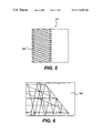
- FIG. 5 is a partial perspective view of an alternative embodiment of a tuning device made in accordance with the present invention.
- FIG. 6 is an enlarged portion of the tuning device shown in FIG. 5 illustrating how light energy may be reflected off the surface of the device.
- FIG. 7 is a graphical representation of the results obtained in the Example which follows.
- a rapid thermal processing apparatus uses intense light to heat a semiconductor wafer as part of the manufacturing process of integrated circuits. Exposure to light energy, which is also referred to herein as light energy, causes a rapid increase in the temperature of a semiconductor wafer and allows processing times to be relatively short. In rapid thermal processing systems, it is important to radiate the wafer with very high intensity light in a very uniform and controlled fashion. As stated above, the difficulty with current devices is that the requirements for the intensity of the radiated light and the ability to heat wafers uniformly are very difficult to achieve.
- the present invention is directed to an apparatus and method for heating semiconductor wafers uniformly and at a controlled rate.
- the apparatus includes a thermal processing chamber in communication with a heating device that is used to heat treat semiconductor wafers contained in the chamber.
- the heating device contains a plurality of lamps that are positioned at preselected locations for heating the wafers. In particular, the lamps emit light energy and form a irradiance distribution over the surface of the wafer.
- the wafer is rotated with respect to the plurality of lamps. In this manner, the lamps form radial heating zones on the wafer.
- the energy supplied to each heating zone can be controlled while the wafer is being heated.
- the temperature at different locations of the wafer is monitored. Based upon the temperature sensed at the different locations, the energy being emitted by the lamps is selectively controlled.
- the heating device in communication with the thermal processing chamber further contains tuning devices which are designed to modify the irradiance distribution of the heating lamps for more uniformly heating the semiconductor wafer.
- the tuning devices allow fine adjustments to be made to the wafer irradiance distribution pattern in order to heat the wafer under a more controlled temperature regime and more uniformly.
- the tuning device can be, in one embodiment, a localized and focused source of light energy that can be directed onto a particular location on the wafer. In an alternative embodiment, however, the tuning device can be a passive device which redirects light energy being emitted by the heating lamps in a manner that heats the wafer more uniformly.
- the tunning device can be an active localized source such as a tungsten halogen bulb in an optical configuration or a laser diode with relatively high power.
- the tuning device can be a passive device that is used to distort and optimize the radiation of the light energy sources and create a desired uniform illumination.
- System 10 includes a processing chamber 12 adapted to receive substrates such as a wafer 14 for conducting various processes. As shown, wafer 14 is positioned on a substrate holder 15 made from a thermal insulating material such as quartz. Chamber 12 is designed to heat wafer 14 at very rapid rates and under carefully controlled conditions. Chamber 12 can be made from various materials, including metals and ceramics. For instance, chamber 12 can be made from stainless steel or quartz.
- chamber 12 When chamber 12 is made from a heat conductive material, preferably the chamber includes a cooling system.
- chamber 12 includes a cooling conduit 16 wrapped around the perimeter of the chamber.
- Conduit 16 is adapted to circulate a cooling fluid, such as water, which is used to maintain the walls of chamber 12 at a constant temperature.
- Chamber 12 can also include a gas inlet 18 and a gas outlet 20 for introducing a gas into the chamber and/or for maintaining the chamber within a preset pressure range.
- a gas can be introduced into chamber 12 through gas inlet 18 for reaction with wafer 14 . Once processed, the gas can then be evacuated from the chamber using gas outlet 20 .
- an inert gas can be fed to chamber 12 through gas inlet 18 for preventing any unwanted or undesirable side reactions from occurring within the chamber.
- gas inlet 18 and gas outlet 20 can be used to pressurize chamber 12 .
- a vacuum can also be created in chamber 12 when desired, using gas outlet 20 or an additional larger outlet positioned beneath the level of the wafer.
- substrate holder 15 can be adapted to rotate wafer 14 using a wafer rotation mechanism 21 .
- Rotating the wafer promotes greater temperature uniformity over the surface of the wafer and promotes enhanced contact between wafer 14 and any gases introduced into the chamber.
- chamber 12 is also adapted to process optical parts, films, fibers, ribbons, and other substrates having any particular shape.
- a heat source or heating device generally 22 is included in communication with chamber 12 for heating wafer 14 during processing.
- Heating device 22 includes a plurality of lamps 24 , such as tungsten-halogen lamps. As shown in FIG. 1, lamps 24 are placed above wafer 14 . It should be understood, however, that lamps 24 may be placed at any particular location. Further, additional lamps could be included within system 10 if desired.
- lamps 24 as a heat source is generally preferred. For instance, lamps have much higher heating and cooling rates than other heating devices, such as electrical elements or conventional furnaces. Lamps 24 create a rapid isothermal processing system that provide instantaneous energy, typically requiring a very short and well controlled start up period. The flow of energy from lamps 24 can also be abruptly stopped at any time. As shown in the figure, lamps 24 are equipped with a gradual power controller 25 that can be used to increase or decrease the light energy being emitted by any of the lamps.
- the lamps can be associated with a reflector or a set of reflectors.
- mounting base 34 can include a reflective surface that surrounds the lamps.
- reflective angular recesses can be formed into a mounting base 34 for directing the light energy onto the wafer.
- heating device 22 can include arc-shaped reflector plates 36 which are located in between the concentric rings of lamps 24 .
- Reflector plates 36 are substantially vertically oriented with respect to a wafer placed in communication with heating device 22 and extend at least a portion of the length of lamps 24 . More particularly, arc-shaped reflector plates 36 can extend less than the length of lamps 24 about the same length as lamps 24 or beyond the length of lamps 24 . Reflector plates 36 serve to direct the light energy being emitted by the concentric rings of lamps. Besides arc-shaped reflector plates 36 , however, it should be understood that various other reflective devices may be used in heating device 22 .
- thermal processing chamber 12 includes plurality of radiation sensing devices generally 27 .
- Radiation sensing devices 27 include a plurality of optical fibers or light pipes 28 which are, in turn, in communication with a plurality of corresponding light detectors 30 .
- Optical fibers 28 are configured to receive thermal energy being emitted by wafer 14 at a particular wavelength. The amount of sensed radiation is then communicated to light detectors 30 which generate a usable voltage signal for determining the temperature of the wafer which can be calculated based, in part, on Planck's Law.
- each optical fiber 28 in combination with a light detector 30 comprises a pyrometer.
- the optical fibers 28 are routed to a single but multiplexing radiation sensing device.
- thermal processing chamber 12 can contain one or a plurality of radiation sensing devices.
- thermal processing chamber 12 contains a plurality of radiation sensing devices that measure the temperature of the wafer at different locations. Knowing the temperature of the wafer at different locations can then be used to control the amount of heat being applied to the wafer as will be described in more detail hereinafter.
- the amount of heat applied to various zones of the wafer can also be controlled in an open loop fashion. In this configuration the ratios between the various heating zones can be pre-determined after manual optimization. In subsequent processes, these ratios are used with no changes during the heating cycles.
- system 10 should be designed such that optical fibers 28 only detect thermal radiation being emitted by wafer 14 and not detect radiation being emitted by lamps 24 .
- system 10 includes a filter 32 which prevents thermal radiation being emitted by lamps 24 at the wavelength at which light detectors 30 operate from entering chamber 12 .
- Filter 32 also serves to isolate lamps 24 from wafer 14 and prevent contamination of the chamber.
- Filter 32 as shown in FIG. 1 can be a window positioned between chamber 12 and heat source 22 .
- each lamp 24 can be covered by a separate filter.
- filter 32 is made from fused silica or quartz.
- Fused silica is known to absorb thermal radiation very effectively at selected wavelengths.
- synthetic fused silica with high concentration of OH ions is very effective at absorbing light at a wavelength of from approximately 2.7 micrometers to about 2.8 micrometers.
- light detectors 30 can be configured to detect thermal radiation being emitted by wafer 14 at a wavelength of about 2.7 micrometers.
- the separation between radiation arriving to the sensor from the wafer and lamps is achieved by mechanical means of isolation.
- buffers and shields are present to prevent a direct path from forming between a light source and a sensing port.
- thermocouples may be incorporated into the system for monitoring the temperature of the wafer at a single location or at a plurality of locations.
- the thermocouples can be placed in direct contact with the wafer or can be placed adjacent the wafer from which the temperature can be extrapolated.
- System 10 further includes a system controller 50 which can be, for instance, a microprocessor.
- Controller 50 receives voltage signals from light detectors 30 that represent the radiation amounts being sampled at the various locations. Based on the signals received, controller 50 is configured to calculate the temperature of wafer 14 at different locations.
- System controller 50 as shown in FIG. 1 can also be in communication with lamp power controller 25 .
- controller 50 can determine the temperature of wafer 14 , and, based on this information, control the amount of thermal energy being emitted by lamps 24 . In this manner, instantaneous adjustments can be made regarding the conditions within reactor 12 for processing wafer 14 within carefully controlled limits.
- controller 50 can also be used to automatically control other elements within the system. For instance, controller 50 can be used to control the flow rate of gases entering chamber 12 through gas inlet 18 . As shown, controller 50 can further be used to control the rate at which wafer 14 is rotated within the chamber.
- heating device 22 includes a plurality of light energy sources, such as lamps 24 that are secured to a mounting base 34 .
- lamps 24 are arranged in five concentric rings which each serve to heat a separate radial zone on a wafer. It should be understood, however, that many other lamp configurations may be used without limitation.
- heating device 22 further includes tuning devices 40 which, in this embodiment, are generally positioned in between the concentric rings of lamps 24 .
- Tuning devices 40 are designed to emit controlled and focused amounts of light energy onto particular locations of a semiconductor wafer being heated.
- the tuning devices are provided in order to make fine adjustments to the irradiance distribution produced by lamps 24 in order to more precisely heat the wafers.
- tuning devices 40 can be used to emit controlled amounts of light energy between the radial heating zones located on the wafer.
- Tuning devices 40 as shown in FIG. 2 are active localized sources of focused light energy.
- the tuning devices can be, for instance, laser diodes having a relatively high power.
- tuning devices 40 can be a lamp, such as a tungsten halogen lamp, in operative association with one or more focusing lenses.
- tuning device 40 includes a light energy source 42 that is spaced a predetermined distance from a first focusing lens 44 and a second focusing lens 46 . Focusing lenses 44 and 46 are designed to focus a beam of light energy being emitted by light energy source 42 onto a desired location of a semiconductor wafer 14 .
- tuning device 40 is recessed in relation to lamps 24 shown in FIG. 2 .
- tuning device 40 is placed behind an opening formed into a wall 48 of heating device 22 .
- Wall 48 as shown in FIG. 2 is located behind lamps 24 . It should be understood, however, that tuning device 40 can also be placed on the other side of wall 48 in the same plane as lamps 24 .
- light energy source 42 and focusing lenses 44 and 46 can be mounted to a support structure 60 .
- Support structure 60 can include a tiltable lever arm which allows for an adjustment to be made in the position of the tuning device.
- support structure 60 can be tilted for focusing light energy being emitted by the light energy source onto desired locations of wafer 14 .
- heating device 22 is preferably in communication with a system controller 50 as shown in FIG. 1 .
- system controller 50 can be designed to vary the amount of light energy being emitted by lamps 24 and by tuning devices 40 .
- Each of the lamps that make up a concentric ring can be controlled together in order to form radial heating zones on the wafer.
- Tuning devices 40 on the other hand, can be controlled by system controller 50 independent of the concentric rings in a manner that enhances temperature uniformity throughout the wafer.
- System controller 50 can also be used to control support structure 60 for automatically directing light energy being emitted by tuning device 40 onto a desired location of the wafer.
- the tuning devices of the present invention can also comprise passive sources which are used to adjust and vary the irradiance distribution of the heating lamps in a manner that enhances wafer temperature uniformity.
- FIG. 4 One embodiment of a system using passive tuning devices is illustrated in FIG. 4 .
- Heating device 122 includes an assembly of lamps 124 secured to a mounting base 134 , which includes a base plate 148 .
- lamps 124 are spaced at various locations on mounting base 134 and are designed to form many different radial heating zones on a wafer.
- heating device 122 further includes tuning devices 140 which are positioned adjacent to selected lamps.
- tuning devices 140 are optical elements designed to redirect a portion of the radiant energy being emitted by the lamp assembly, thereby allowing fine adjustments to the irradiance distribution of the heater device onto a wafer located below the assembly.
- the optical elements are rectangular shaped and are inserted into heating device 122 generally near one or more of the lamps 124 .
- Heater device 122 can be designed such that the depth of insertion of tuning devices 140 and the azimuthal angle of the tuning devices can be adjusted.
- tuning devices 140 can be inserted through an opening formed into base plate 148 and can be extended into the heater device any desired length in relation to the length of lamps 124 .
- the angle at which the tuning devices are inserted can be adjusted.
- tuning devices 140 are to cause the radiation being emitted from lamps 124 to deviate from an original azimuthal direction of propagation in order to modify the radial power distribution on the wafer. Desirably, the light energy being emitted by the lamps exits heater device 122 sooner than it would otherwise without tuning devices 140 and will hit and contact the wafer at a different radial location than it would otherwise. By selectively varying the location of tuning devices 140 , the wafer can be heated under a more controlled and uniform temperature regime.
- tuning devices 140 In order to redirect the light energy that is being emitted by lamps 124 , tuning devices 140 include at least one surface having desired optical characteristics. In modifying the irradiance distribution of the lamps, tuning devices 140 can either reflect light energy, refract light energy, or can even absorb light energy.
- tuning device 140 includes a ruled prismatic surface 162 .
- surface 162 is serrated and mirrored.
- the prismatic surface illustrated in FIG. 5 employs a fixed pitch with a fixed facet angle. It should be understood, however, that the surface could also employ a fixed pitch with a variable facet angle.
- tuning device 140 By including a ruled prismatic surface, tuning device 140 causes radiant energy contacting the device to exit heater device 122 sooner than would otherwise occur. This device alters the radial irradiance distribution of the system in a way that can be finely adjusted over some preestablished range.
- tuning device 140 can also be made with a variable angle design. When using a variable angle design, tuning device 140 can be used to more accurately focus light radiation contacting surface 162 and more accurately redirect the light energy onto a particular location on the wafer being heated if desired.
- surface 162 of tuning device 140 can be planar and diffusing, causing light energy contacting the surface to scatter in all directions.
- a highly diffuse surface may be a rough but highly reflective surface on tuning device 140 .
- Using a diffuse surface may be less costly to produce but may not provide a similar amount of control as using a prismatic surface.
- tuning device 140 can be designed to either reflect light radiation, refract light radiation or absorb light radiation.
- tuning device 140 is coated with a highly reflective material, such as a dielectric material or a polished metal, such as gold, copper, or aluminum.
- tuning device 140 can be made, for instance, from quartz.
- a prismatic tuning device similar to the one illustrated in FIG. 5 was inserted into an array of light energy sources in a thermal processing chamber.
- the array of light energy sources included five concentric rings of vertically orientated lamps mounted to a base, similar to the heating device illustrated in FIG. 4 .
- the prismatic tuning device was positioned adjacent one of the lamps located on the second concentric ring from the center of the array of lamps.
- the tuning device of the present invention changed the irradiance distribution of the light energy sources of particular advantage, the tuning device only slightly modified the irradiance distribution.
- the tuning device of the present invention is well suited to making fine adjustments in the manner in which a wafer is illuminated in order to promote temperature uniformity.
Landscapes
- Engineering & Computer Science (AREA)
- Mechanical Engineering (AREA)
- General Engineering & Computer Science (AREA)
- Testing Or Measuring Of Semiconductors Or The Like (AREA)
Abstract
Description
Claims (40)
Priority Applications (11)
| Application Number | Priority Date | Filing Date | Title |
|---|---|---|---|
| US09/226,396 US6771895B2 (en) | 1999-01-06 | 1999-01-06 | Heating device for heating semiconductor wafers in thermal processing chambers |
| TW089100171A TW504728B (en) | 1999-01-06 | 2000-01-06 | Heating device for heating semiconductor wafers in thermal processing chambers |
| AU22246/00A AU2224600A (en) | 1999-01-06 | 2000-01-06 | Heating device for heating semiconductor wafers in thermal processing chambers |
| EP00901398A EP1141999A1 (en) | 1999-01-06 | 2000-01-06 | Heating device for heating semiconductor wafers in thermal processing chambers |
| US09/478,247 US6717158B1 (en) | 1999-01-06 | 2000-01-06 | Heating device for heating semiconductor wafers in thermal processing chambers |
| PCT/US2000/000228 WO2000041223A1 (en) | 1999-01-06 | 2000-01-06 | Heating device for heating semiconductor wafers in thermal processing chambers |
| KR1020017008610A KR100729006B1 (en) | 1999-01-06 | 2000-01-06 | Heating device for heating semiconductor wafers in thermal processing chambers |
| JP2000592867A JP2002534803A (en) | 1999-01-06 | 2000-01-06 | Heating device for heating semiconductor wafer in heat treatment chamber |
| US10/903,424 US7038174B2 (en) | 1999-01-06 | 2004-07-30 | Heating device for heating semiconductor wafers in thermal processing chambers |
| US11/399,085 US7608802B2 (en) | 1999-01-06 | 2006-04-06 | Heating device for heating semiconductor wafers in thermal processing chambers |
| US12/574,441 US8138451B2 (en) | 1999-01-06 | 2009-10-06 | Heating device for heating semiconductor wafers in thermal processing chambers |
Applications Claiming Priority (1)
| Application Number | Priority Date | Filing Date | Title |
|---|---|---|---|
| US09/226,396 US6771895B2 (en) | 1999-01-06 | 1999-01-06 | Heating device for heating semiconductor wafers in thermal processing chambers |
Related Child Applications (2)
| Application Number | Title | Priority Date | Filing Date |
|---|---|---|---|
| US09/478,247 Continuation-In-Part US6717158B1 (en) | 1999-01-06 | 2000-01-06 | Heating device for heating semiconductor wafers in thermal processing chambers |
| US10/903,424 Continuation US7038174B2 (en) | 1999-01-06 | 2004-07-30 | Heating device for heating semiconductor wafers in thermal processing chambers |
Publications (2)
| Publication Number | Publication Date |
|---|---|
| US20020017618A1 US20020017618A1 (en) | 2002-02-14 |
| US6771895B2 true US6771895B2 (en) | 2004-08-03 |
Family
ID=22848749
Family Applications (5)
| Application Number | Title | Priority Date | Filing Date |
|---|---|---|---|
| US09/226,396 Expired - Lifetime US6771895B2 (en) | 1999-01-06 | 1999-01-06 | Heating device for heating semiconductor wafers in thermal processing chambers |
| US09/478,247 Expired - Lifetime US6717158B1 (en) | 1999-01-06 | 2000-01-06 | Heating device for heating semiconductor wafers in thermal processing chambers |
| US10/903,424 Expired - Lifetime US7038174B2 (en) | 1999-01-06 | 2004-07-30 | Heating device for heating semiconductor wafers in thermal processing chambers |
| US11/399,085 Expired - Fee Related US7608802B2 (en) | 1999-01-06 | 2006-04-06 | Heating device for heating semiconductor wafers in thermal processing chambers |
| US12/574,441 Expired - Fee Related US8138451B2 (en) | 1999-01-06 | 2009-10-06 | Heating device for heating semiconductor wafers in thermal processing chambers |
Family Applications After (4)
| Application Number | Title | Priority Date | Filing Date |
|---|---|---|---|
| US09/478,247 Expired - Lifetime US6717158B1 (en) | 1999-01-06 | 2000-01-06 | Heating device for heating semiconductor wafers in thermal processing chambers |
| US10/903,424 Expired - Lifetime US7038174B2 (en) | 1999-01-06 | 2004-07-30 | Heating device for heating semiconductor wafers in thermal processing chambers |
| US11/399,085 Expired - Fee Related US7608802B2 (en) | 1999-01-06 | 2006-04-06 | Heating device for heating semiconductor wafers in thermal processing chambers |
| US12/574,441 Expired - Fee Related US8138451B2 (en) | 1999-01-06 | 2009-10-06 | Heating device for heating semiconductor wafers in thermal processing chambers |
Country Status (7)
| Country | Link |
|---|---|
| US (5) | US6771895B2 (en) |
| EP (1) | EP1141999A1 (en) |
| JP (1) | JP2002534803A (en) |
| KR (1) | KR100729006B1 (en) |
| AU (1) | AU2224600A (en) |
| TW (1) | TW504728B (en) |
| WO (1) | WO2000041223A1 (en) |
Cited By (15)
| Publication number | Priority date | Publication date | Assignee | Title |
|---|---|---|---|---|
| US20040070415A1 (en) * | 2002-10-02 | 2004-04-15 | Stefan Schneidewind | Test apparatus for testing substrates at low temperatures |
| US20050098552A1 (en) * | 2002-11-05 | 2005-05-12 | Timans Paul J. | Apparatus and method for reducing stray light in substrate processing chambers |
| US20050173386A1 (en) * | 2004-01-20 | 2005-08-11 | Matsushita Electric Industrial Co., Ltd. | Light irradiation heat treatment method and light irradiation heat treatment apparatus |
| US20050189329A1 (en) * | 2003-09-02 | 2005-09-01 | Somit Talwar | Laser thermal processing with laser diode radiation |
| US20050211697A1 (en) * | 2004-03-26 | 2005-09-29 | Knutson Karson L | Multi-zone reflecting device for use in flash lamp processes |
| US20050213949A1 (en) * | 2000-12-21 | 2005-09-29 | Zion Koren | Heating configuration for use in thermal processing chambers |
| US20060096951A1 (en) * | 2004-10-29 | 2006-05-11 | International Business Machines Corporation | Apparatus and method for controlling process non-uniformity |
| US7226488B2 (en) | 1998-11-20 | 2007-06-05 | Mattson Technology, Inc. | Fast heating and cooling apparatus for semiconductor wafers |
| US20080008460A1 (en) * | 2001-11-07 | 2008-01-10 | Timans Paul J | System and process for heating semiconductor wafers by optimizing absorption of electromagnetic energy |
| US20130248504A1 (en) * | 2012-03-22 | 2013-09-26 | Dainippon Screen Mfg. Co., Ltd. | Heat treatment apparatus for heating substrate by light irradiation |
| US20130323936A1 (en) * | 2012-05-30 | 2013-12-05 | Lawrence Livermore National Security, Llc | Apparatus and methods for rapid thermal processing |
| US8624165B2 (en) | 2010-09-16 | 2014-01-07 | Dainippon Screen Mfg. Co., Ltd. | Heat treatment apparatus for heating substrate by irradiating substrate with flashes of light |
| US9113501B2 (en) | 2012-05-25 | 2015-08-18 | Watlow Electric Manufacturing Company | Variable pitch resistance coil heater |
| US20170103907A1 (en) * | 2015-10-09 | 2017-04-13 | Applied Materials, Inc. | Diode laser for wafer heating for epi processes |
| US10029332B2 (en) | 2014-09-04 | 2018-07-24 | Samsung Electronics Co., Ltd. | Spot heater and device for cleaning wafer using the same |
Families Citing this family (71)
| Publication number | Priority date | Publication date | Assignee | Title |
|---|---|---|---|---|
| DE19952017A1 (en) * | 1999-10-28 | 2001-05-17 | Steag Rtp Systems Gmbh | Method and device for the thermal treatment of substrates |
| US6594446B2 (en) * | 2000-12-04 | 2003-07-15 | Vortek Industries Ltd. | Heat-treating methods and systems |
| US6902622B2 (en) | 2001-04-12 | 2005-06-07 | Mattson Technology, Inc. | Systems and methods for epitaxially depositing films on a semiconductor substrate |
| US7445382B2 (en) | 2001-12-26 | 2008-11-04 | Mattson Technology Canada, Inc. | Temperature measurement and heat-treating methods and system |
| US7734439B2 (en) * | 2002-06-24 | 2010-06-08 | Mattson Technology, Inc. | System and process for calibrating pyrometers in thermal processing chambers |
| US7101812B2 (en) | 2002-09-20 | 2006-09-05 | Mattson Technology, Inc. | Method of forming and/or modifying a dielectric film on a semiconductor surface |
| AU2003287837A1 (en) * | 2002-12-20 | 2004-07-14 | Vortek Industries Ltd | Methods and systems for supporting a workpiece and for heat-treating the workpiece |
| US7654596B2 (en) | 2003-06-27 | 2010-02-02 | Mattson Technology, Inc. | Endeffectors for handling semiconductor wafers |
| US6862404B1 (en) * | 2003-09-08 | 2005-03-01 | Wafermasters | Focused photon energy heating chamber |
| US20080090309A1 (en) * | 2003-10-27 | 2008-04-17 | Ranish Joseph M | Controlled annealing method |
| US20070179677A1 (en) * | 2003-11-25 | 2007-08-02 | Polymer Innovation, Llc | Self contained bench top enclosure temperature control system |
| US7645356B2 (en) * | 2003-11-25 | 2010-01-12 | International Business Machines Corporation | Method of processing wafers with resonant heating |
| US7283734B2 (en) * | 2004-08-24 | 2007-10-16 | Fujitsu Limited | Rapid thermal processing apparatus and method of manufacture of semiconductor device |
| DE102004060557A1 (en) * | 2004-12-16 | 2006-06-29 | Forschungszentrum Rossendorf E.V. | Flash lamp mirror arrangement |
| DE102005010005A1 (en) * | 2005-03-04 | 2006-12-28 | Nunner, Dieter | Apparatus and method for coating small parts |
| WO2007005489A2 (en) * | 2005-07-05 | 2007-01-11 | Mattson Technology, Inc. | Method and system for determining optical properties of semiconductor wafers |
| CN101288035B (en) * | 2005-09-14 | 2013-06-19 | 马特森技术有限公司 | Method and apparatus for repeatable heat treatment |
| US7184657B1 (en) | 2005-09-17 | 2007-02-27 | Mattson Technology, Inc. | Enhanced rapid thermal processing apparatus and method |
| JP2007095889A (en) * | 2005-09-28 | 2007-04-12 | Ushio Inc | Light irradiation heating method |
| JP5168788B2 (en) * | 2006-01-23 | 2013-03-27 | 信越半導体株式会社 | Manufacturing method of SOI wafer |
| US7543981B2 (en) | 2006-06-29 | 2009-06-09 | Mattson Technology, Inc. | Methods for determining wafer temperature |
| US7976634B2 (en) * | 2006-11-21 | 2011-07-12 | Applied Materials, Inc. | Independent radiant gas preheating for precursor disassociation control and gas reaction kinetics in low temperature CVD systems |
| US9536728B2 (en) * | 2007-02-15 | 2017-01-03 | Applied Material, Inc. | Lamp for rapid thermal processing chamber |
| CN101702950B (en) * | 2007-05-01 | 2012-05-30 | 加拿大马特森技术有限公司 | Irradiance pulse heat-treating methods and apparatus |
| DE102007058002B4 (en) * | 2007-12-03 | 2016-03-17 | Mattson Thermal Products Gmbh | Device for the thermal treatment of disc-shaped semiconductor substrates |
| US7976216B2 (en) | 2007-12-20 | 2011-07-12 | Mattson Technology, Inc. | Determining the temperature of silicon at high temperatures |
| US8314368B2 (en) * | 2008-02-22 | 2012-11-20 | Applied Materials, Inc. | Silver reflectors for semiconductor processing chambers |
| WO2009137940A1 (en) | 2008-05-16 | 2009-11-19 | Mattson Technology Canada, Inc. | Workpiece breakage prevention method and apparatus |
| US20100068898A1 (en) * | 2008-09-17 | 2010-03-18 | Stephen Moffatt | Managing thermal budget in annealing of substrates |
| CN102160157B (en) * | 2008-09-17 | 2015-11-25 | 应用材料公司 | The heat budget of management annealing of substrates |
| US8314369B2 (en) * | 2008-09-17 | 2012-11-20 | Applied Materials, Inc. | Managing thermal budget in annealing of substrates |
| KR101031226B1 (en) | 2009-08-21 | 2011-04-29 | 에이피시스템 주식회사 | Heater Block of Rapid Heat Treatment Device |
| JP5519329B2 (en) * | 2010-02-26 | 2014-06-11 | 東京エレクトロン株式会社 | Method for heating parts in processing chamber of semiconductor manufacturing apparatus and semiconductor manufacturing apparatus |
| US20120181265A1 (en) * | 2010-07-15 | 2012-07-19 | Despatch Industries Limited Partnership | Firing furnace configuration for thermal processing system |
| KR101733179B1 (en) | 2010-10-15 | 2017-05-08 | 맛선 테크놀러지, 인코포레이티드 | Methods, apparatus and media for determining a shape of an irradiance pulse to which a workpiece is to be exposed |
| DE102011116243B4 (en) * | 2011-10-17 | 2014-04-17 | Centrotherm Photovoltaics Ag | Device for determining the temperature of a substrate |
| KR101368818B1 (en) * | 2012-05-03 | 2014-03-04 | 에이피시스템 주식회사 | Apparatus for substrate treatment |
| KR101503117B1 (en) * | 2012-08-31 | 2015-03-16 | 엘지디스플레이 주식회사 | Curing apparatus |
| US20140270731A1 (en) * | 2013-03-12 | 2014-09-18 | Applied Materials, Inc. | Thermal management apparatus for solid state light source arrays |
| KR101572662B1 (en) * | 2013-12-18 | 2015-11-27 | 에이피시스템 주식회사 | Apparatus for processing substrate |
| WO2015107009A1 (en) | 2014-01-17 | 2015-07-23 | Koninklijke Philips N.V. | Heating system comprising semiconductor light sources |
| TWI686100B (en) * | 2014-11-28 | 2020-02-21 | 日商日本碍子股份有限公司 | Infrared heater and infrared processing device |
| WO2016122835A1 (en) * | 2015-01-30 | 2016-08-04 | Applied Materials, Inc. | Lamp heating for process chamber |
| CN107851580B (en) | 2015-07-29 | 2022-10-18 | 应用材料公司 | Laser annealing of rotating substrates |
| US10932323B2 (en) * | 2015-08-03 | 2021-02-23 | Alta Devices, Inc. | Reflector and susceptor assembly for chemical vapor deposition reactor |
| US20170194133A1 (en) * | 2015-12-30 | 2017-07-06 | Mattson Technology, Inc. | Electrode Tip for ARC Lamp |
| US10770309B2 (en) * | 2015-12-30 | 2020-09-08 | Mattson Technology, Inc. | Features for improving process uniformity in a millisecond anneal system |
| US10727094B2 (en) | 2016-01-29 | 2020-07-28 | Taiwan Semiconductor Manufacturing Co., Ltd | Thermal reflector device for semiconductor fabrication tool |
| DE102017012389B4 (en) | 2016-05-13 | 2024-12-19 | OSRAM Opto Semiconductors Gesellschaft mit beschränkter Haftung | semiconductor chip |
| DE102017109812A1 (en) | 2016-05-13 | 2017-11-16 | Osram Opto Semiconductors Gmbh | Light-emitting semiconductor chip and method for producing a light-emitting semiconductor chip |
| DE102017109809B4 (en) | 2016-05-13 | 2024-01-18 | OSRAM Opto Semiconductors Gesellschaft mit beschränkter Haftung | Method for producing a semiconductor chip |
| JP6736386B2 (en) * | 2016-07-01 | 2020-08-05 | 東京エレクトロン株式会社 | Substrate liquid processing apparatus, substrate liquid processing method and recording medium |
| KR102145276B1 (en) | 2016-07-22 | 2020-08-18 | 어플라이드 머티어리얼스, 인코포레이티드 | Heating modulator to improve epi-uniformity adjustment |
| DE102016119703A1 (en) * | 2016-10-17 | 2018-04-19 | Kraussmaffei Technologies Gmbh | Method and device for producing molded parts with a semi-finished product |
| JP6845730B2 (en) | 2017-04-18 | 2021-03-24 | 株式会社Screenホールディングス | Heat treatment equipment |
| JP7191504B2 (en) * | 2017-07-14 | 2022-12-19 | 株式会社Screenホールディングス | Heat treatment equipment |
| JP2019021828A (en) * | 2017-07-20 | 2019-02-07 | 株式会社Screenホールディングス | Heat treatment equipment |
| CN108287574B (en) * | 2018-03-29 | 2025-12-09 | 紫石能源有限公司 | Temperature adjusting device and wafer vacuum heating device |
| JP7274512B2 (en) * | 2018-06-26 | 2023-05-16 | アプライド マテリアルズ インコーポレイテッド | Method and apparatus for measuring temperature |
| KR102711233B1 (en) | 2018-08-03 | 2024-09-30 | 어플라이드 머티어리얼스, 인코포레이티드 | Multi-zone lamp control and individual lamp control at the lamphead |
| CN111564532B (en) * | 2020-04-03 | 2023-02-17 | 江西昌大高新能源材料技术有限公司 | A kind of HAC solar cell post-processing efficiency enhancement equipment and method |
| CN111725114B (en) * | 2020-06-30 | 2023-07-14 | 北京北方华创微电子装备有限公司 | Position correction device for heating lamps |
| US11430671B2 (en) * | 2020-07-30 | 2022-08-30 | Taiwan Semiconductor Manufacturing Co., Ltd. | Ozone wafer cleaning module having an ultraviolet lamp module with rotatable reflectors |
| US12033874B2 (en) | 2020-09-03 | 2024-07-09 | Applied Materials, Inc. | EPI chamber with full wafer laser heating |
| US20220367216A1 (en) * | 2021-05-11 | 2022-11-17 | Applied Materials, Inc. | Multi-zone lamp heating and temperature monitoring in epitaxy process chamber |
| KR102766146B1 (en) * | 2021-11-11 | 2025-02-12 | 에이피시스템 주식회사 | Apparatus and methode for processing substrate |
| CN115379600B (en) * | 2022-05-30 | 2025-02-11 | 南京原磊纳米材料有限公司 | Epitaxial annular infrared halogen heating component and steady-state temperature field acquisition method |
| KR102779288B1 (en) * | 2022-09-19 | 2025-03-11 | 에이피시스템 주식회사 | Heater block and apparatus for heating substrate having the same |
| US20240248282A1 (en) * | 2023-01-25 | 2024-07-25 | Applied Materials, Inc. | Apparatus and methods for heating tunability in processing chambers |
| CN116598232A (en) * | 2023-06-26 | 2023-08-15 | 北京屹唐半导体科技股份有限公司 | Heat treatment device and precise temperature measurement method for semiconductor workpiece |
| US20250210381A1 (en) * | 2023-12-22 | 2025-06-26 | Applied Materials, Inc. | Heat reflection assembly for substrate temperature uniformity |
Citations (154)
| Publication number | Priority date | Publication date | Assignee | Title |
|---|---|---|---|---|
| US3623712A (en) | 1969-10-15 | 1971-11-30 | Applied Materials Tech | Epitaxial radiation heated reactor and process |
| US3761678A (en) | 1971-05-03 | 1973-09-25 | Aerojet General Co | High density spherical modules |
| US3796182A (en) | 1971-12-16 | 1974-03-12 | Applied Materials Tech | Susceptor structure for chemical vapor deposition reactor |
| US3830194A (en) | 1972-09-28 | 1974-08-20 | Applied Materials Tech | Susceptor support structure and docking assembly |
| US3836751A (en) | 1973-07-26 | 1974-09-17 | Applied Materials Inc | Temperature controlled profiling heater |
| US3862397A (en) | 1972-03-24 | 1975-01-21 | Applied Materials Tech | Cool wall radiantly heated reactor |
| US4001047A (en) | 1975-05-19 | 1977-01-04 | General Electric Company | Temperature gradient zone melting utilizing infrared radiation |
| US4041278A (en) | 1975-05-19 | 1977-08-09 | General Electric Company | Heating apparatus for temperature gradient zone melting |
| US4047496A (en) | 1974-05-31 | 1977-09-13 | Applied Materials, Inc. | Epitaxial radiation heated reactor |
| US4048955A (en) | 1975-09-02 | 1977-09-20 | Texas Instruments Incorporated | Continuous chemical vapor deposition reactor |
| US4081313A (en) | 1975-01-24 | 1978-03-28 | Applied Materials, Inc. | Process for preparing semiconductor wafers with substantially no crystallographic slip |
| US4097226A (en) | 1976-10-26 | 1978-06-27 | General Electric Company | Furnace for practising temperature gradient zone melting |
| US4115163A (en) | 1976-01-08 | 1978-09-19 | Yulia Ivanovna Gorina | Method of growing epitaxial semiconductor films utilizing radiant heating |
| US4184065A (en) | 1977-04-28 | 1980-01-15 | Nichiden Machinery, Limited | Heating apparatus having ellipsoidal reflecting mirror |
| US4221956A (en) | 1978-06-21 | 1980-09-09 | General Electric Company | Apparatus for practising temperature gradient zone melting |
| US4224504A (en) | 1978-06-21 | 1980-09-23 | General Electric Company | Apparatus for practicing temperature gradient zone melting |
| US4389970A (en) | 1981-03-16 | 1983-06-28 | Energy Conversion Devices, Inc. | Apparatus for regulating substrate temperature in a continuous plasma deposition process |
| US4436985A (en) | 1982-05-03 | 1984-03-13 | Gca Corporation | Apparatus for heat treating semiconductor wafers |
| US4446817A (en) | 1980-12-20 | 1984-05-08 | Cambridge Instruments Limited | Apparatus for vapor deposition of a film on a substrate |
| US4470369A (en) | 1982-07-12 | 1984-09-11 | Energy Conversion Devices, Inc. | Apparatus for uniformly heating a substrate |
| US4477718A (en) | 1983-01-10 | 1984-10-16 | Radiant Technology Corporation | Infrared furnace with controlled environment |
| US4496828A (en) | 1983-07-08 | 1985-01-29 | Ultra Carbon Corporation | Susceptor assembly |
| US4504730A (en) | 1983-10-04 | 1985-03-12 | Ushio Denki Kabushiki Kaisha | Method for heating semiconductor wafer by means of application of radiated light |
| US4504323A (en) | 1980-09-12 | 1985-03-12 | Ushio Denki Kabushiki Kaisha | Method for annealing semiconductors with a planar source composed of flash discharge lamps |
| US4508960A (en) | 1982-08-30 | 1985-04-02 | Ushio Denki Kabushiki Kaisha | Light-radiant furnace |
| US4511788A (en) | 1983-02-09 | 1985-04-16 | Ushio Denki Kabushiki Kaisha | Light-radiant heating furnace |
| US4517448A (en) | 1981-03-23 | 1985-05-14 | Radiant Technology Corporation | Infrared furnace with atmosphere control capability |
| US4533820A (en) | 1982-06-25 | 1985-08-06 | Ushio Denki Kabushiki Kaisha | Radiant heating apparatus |
| US4540876A (en) | 1983-03-18 | 1985-09-10 | U.S. Philips Corporation | Furnace suitable for heat-treating semiconductor bodies |
| US4543472A (en) | 1982-11-03 | 1985-09-24 | Ushio Denki Kabushiki Kaisha | Plane light source unit and radiant heating furnace including same |
| US4544418A (en) | 1984-04-16 | 1985-10-01 | Gibbons James F | Process for high temperature surface reactions in semiconductor material |
| US4545327A (en) | 1982-08-27 | 1985-10-08 | Anicon, Inc. | Chemical vapor deposition apparatus |
| US4550245A (en) | 1982-10-26 | 1985-10-29 | Ushio Denki Kabushiki Kaisha | Light-radiant furnace for heating semiconductor wafers |
| US4551616A (en) | 1983-07-07 | 1985-11-05 | Thorn Emi Domestic Appliances Limited | Heating apparatus |
| US4558660A (en) | 1982-03-16 | 1985-12-17 | Handotai Kenkyu Shinkokai | Semiconductor fabricating apparatus |
| US4567352A (en) | 1983-03-29 | 1986-01-28 | Ushio Denki Kabushiki Kaisha | Flashlight-radiant apparatus |
| US4571486A (en) | 1983-03-16 | 1986-02-18 | Ushio Denki Kabushiki Kaisha | Heating method of semiconductor wafer |
| US4581520A (en) | 1982-09-07 | 1986-04-08 | Vu Duy Phach | Heat treatment machine for semiconductors |
| US4607591A (en) | 1985-08-06 | 1986-08-26 | Spectrum Cvd, Inc. | CVD heater control circuit |
| US4615294A (en) | 1984-07-31 | 1986-10-07 | Hughes Aircraft Company | Barrel reactor and method for photochemical vapor deposition |
| US4632056A (en) | 1985-08-05 | 1986-12-30 | Stitz Robert W | CVD temperature control |
| US4632057A (en) | 1985-08-05 | 1986-12-30 | Spectrum Cvd, Inc. | CVD plasma reactor |
| US4640224A (en) | 1985-08-05 | 1987-02-03 | Spectrum Cvd, Inc. | CVD heat source |
| US4642243A (en) | 1982-09-20 | 1987-02-10 | Semiconductor Energy Laboratory Co., Ltd. | Method and apparatus for forming non-single-crystal layer |
| US4649261A (en) | 1984-02-28 | 1987-03-10 | Tamarack Scientific Co., Inc. | Apparatus for heating semiconductor wafers in order to achieve annealing, silicide formation, reflow of glass passivation layers, etc. |
| US4653428A (en) | 1985-05-10 | 1987-03-31 | General Electric Company | Selective chemical vapor deposition apparatus |
| US4654509A (en) | 1985-10-07 | 1987-03-31 | Epsilon Limited Partnership | Method and apparatus for substrate heating in an axially symmetric epitaxial deposition apparatus |
| US4680451A (en) | 1985-07-29 | 1987-07-14 | A. G. Associates | Apparatus using high intensity CW lamps for improved heat treating of semiconductor wafers |
| US4694143A (en) | 1985-02-26 | 1987-09-15 | Mitsubishi Denki Kabushiki Kaisha | Zone melting apparatus for monocrystallizing semiconductor layer on insulator layer |
| US4698486A (en) | 1984-02-28 | 1987-10-06 | Tamarack Scientific Co., Inc. | Method of heating semiconductor wafers in order to achieve annealing, silicide formation, reflow of glass passivation layers, etc. |
| US4761538A (en) | 1985-11-21 | 1988-08-02 | Dainippon Screen Mfg. Co., Ltd. | Method and apparatus for controlling the temperature of a radiantly heated object |
| US4789771A (en) | 1985-10-07 | 1988-12-06 | Epsilon Limited Partnership | Method and apparatus for substrate heating in an axially symmetric epitaxial deposition apparatus |
| US4796562A (en) | 1985-12-03 | 1989-01-10 | Varian Associates, Inc. | Rapid thermal cvd apparatus |
| US4806321A (en) | 1984-07-26 | 1989-02-21 | Research Development Corporation Of Japan | Use of infrared radiation and an ellipsoidal reflection mirror |
| EP0308388A1 (en) | 1987-09-14 | 1989-03-22 | Jules Lefevere | Electrical heating apparatus |
| US4817558A (en) | 1986-07-10 | 1989-04-04 | Kabushiki Kaisha Toshiba | Thin-film depositing apparatus |
| US4820377A (en) | 1987-07-16 | 1989-04-11 | Texas Instruments Incorporated | Method for cleanup processing chamber and vacuum process module |
| US4820906A (en) | 1987-03-13 | 1989-04-11 | Peak Systems, Inc. | Long arc lamp for semiconductor heating |
| US4830700A (en) | 1987-07-16 | 1989-05-16 | Texas Instruments Incorporated | Processing apparatus and method |
| US4832779A (en) | 1987-07-16 | 1989-05-23 | Texas Instruments Incorporated | Processing apparatus |
| US4832778A (en) | 1987-07-16 | 1989-05-23 | Texas Instruments Inc. | Processing apparatus for wafers |
| US4832777A (en) | 1987-07-16 | 1989-05-23 | Texas Instruments Incorporated | Processing apparatus and method |
| US4836138A (en) | 1987-06-18 | 1989-06-06 | Epsilon Technology, Inc. | Heating system for reaction chamber of chemical vapor deposition equipment |
| US4854263A (en) | 1987-08-14 | 1989-08-08 | Applied Materials, Inc. | Inlet manifold and methods for increasing gas dissociation and for PECVD of dielectric films |
| US4857704A (en) | 1986-02-19 | 1989-08-15 | Bertin & Cie | Apparatus for thermal treatments of thin parts such as silicon wafers |
| US4857139A (en) | 1984-11-26 | 1989-08-15 | Semiconductor Energy Laboratory Co., Ltd. | Method and apparatus for forming a layer |
| US4859832A (en) | 1986-09-08 | 1989-08-22 | Nikon Corporation | Light radiation apparatus |
| US4901670A (en) | 1988-08-22 | 1990-02-20 | Santa Barbara Research Center | Elemental mercury source for metal-organic chemical vapor deposition |
| US4908495A (en) | 1988-12-20 | 1990-03-13 | Texas Instruments Incorporated | Heating lamp assembly for ccvd reactors |
| US4911103A (en) | 1987-07-17 | 1990-03-27 | Texas Instruments Incorporated | Processing apparatus and method |
| US4913929A (en) | 1987-04-21 | 1990-04-03 | The Board Of Trustees Of The Leland Stanford Junior University | Thermal/microwave remote plasma multiprocessing reactor and method of use |
| US4919077A (en) | 1986-12-27 | 1990-04-24 | Mitsubishi Denki Kabushiki Kaisha | Semiconductor producing apparatus |
| US4920918A (en) | 1989-04-18 | 1990-05-01 | Applied Materials, Inc. | Pressure-resistant thermal reactor system for semiconductor processing |
| US4924073A (en) | 1988-02-09 | 1990-05-08 | Dainippon Screen Mfg. Co., Ltd. | Method of controlling heat treatment apparatus for substrate |
| US4924807A (en) | 1986-07-26 | 1990-05-15 | Nihon Shinku Gijutsu Kabushiki Kaisha | Apparatus for chemical vapor deposition |
| US4956538A (en) | 1988-09-09 | 1990-09-11 | Texas Instruments, Incorporated | Method and apparatus for real-time wafer temperature measurement using infrared pyrometry in advanced lamp-heated rapid thermal processors |
| US4958061A (en) | 1988-06-27 | 1990-09-18 | Tokyo Electron Limited | Method and apparatus for heat-treating a substrate |
| US4975561A (en) * | 1987-06-18 | 1990-12-04 | Epsilon Technology Inc. | Heating system for substrates |
| US4979466A (en) | 1986-12-01 | 1990-12-25 | Hitachi, Ltd. | Apparatus for selective deposition of metal thin film |
| US4981815A (en) | 1988-05-09 | 1991-01-01 | Siemens Aktiengesellschaft | Method for rapidly thermally processing a semiconductor wafer by irradiation using semicircular or parabolic reflectors |
| US4985281A (en) | 1988-08-22 | 1991-01-15 | Santa Barbara Research Center | Elemental mercury source for metal-organic chemical vapor deposition |
| US4989544A (en) | 1989-01-26 | 1991-02-05 | Canon Kabushiki Kaisha | Apparatus for forming functional deposited films by way of hybrid excitation |
| US5000113A (en) | 1986-12-19 | 1991-03-19 | Applied Materials, Inc. | Thermal CVD/PECVD reactor and use for thermal chemical vapor deposition of silicon dioxide and in-situ multi-step planarized process |
| US5011794A (en) | 1989-05-01 | 1991-04-30 | At&T Bell Laboratories | Procedure for rapid thermal annealing of implanted semiconductors |
| US5038395A (en) | 1988-03-05 | 1991-08-06 | Dornier Gmbh | Reflector furnace |
| US5044943A (en) | 1990-08-16 | 1991-09-03 | Applied Materials, Inc. | Spoked susceptor support for enhanced thermal uniformity of susceptor in semiconductor wafer processing apparatus |
| US5047611A (en) | 1990-03-23 | 1991-09-10 | Peak Systems, Inc. | Method for selectively curing a film on a substrate |
| US5053247A (en) | 1989-02-28 | 1991-10-01 | Moore Epitaxial, Inc. | Method for increasing the batch size of a barrel epitaxial reactor and reactor produced thereby |
| US5057668A (en) | 1987-09-16 | 1991-10-15 | Siemens Aktiengesellschaft | Device for the implementation of a curing process at a semiconductor wafer and method for curing a semiconductor wafer |
| US5073698A (en) | 1990-03-23 | 1991-12-17 | Peak Systems, Inc. | Method for selectively heating a film on a substrate |
| EP0468874A2 (en) | 1990-07-25 | 1992-01-29 | Sumitomo Electric Industries, Ltd. | Lamp annealing process for semiconductor wafer and apparatus for execution of such process |
| US5085887A (en) | 1990-09-07 | 1992-02-04 | Applied Materials, Inc. | Wafer reactor vessel window with pressure-thermal compensation |
| US5108792A (en) | 1990-03-09 | 1992-04-28 | Applied Materials, Inc. | Double-dome reactor for semiconductor processing |
| US5113929A (en) | 1990-04-09 | 1992-05-19 | Anelva Corporation | Temperature control system for semiconductor wafer or substrate |
| US5129360A (en) | 1990-01-24 | 1992-07-14 | The United States Of America As Represented By The Secretary Of The Air Force | Actively cooled effusion cell for chemical vapor deposition |
| US5148714A (en) | 1990-10-24 | 1992-09-22 | Ag Processing Technology, Inc. | Rotary/linear actuator for closed chamber, and reaction chamber utilizing same |
| US5155337A (en) | 1989-12-21 | 1992-10-13 | North Carolina State University | Method and apparatus for controlling rapid thermal processing systems |
| US5154512A (en) | 1990-04-10 | 1992-10-13 | Luxtron Corporation | Non-contact techniques for measuring temperature or radiation-heated objects |
| US5156820A (en) | 1989-05-15 | 1992-10-20 | Rapro Technology, Inc. | Reaction chamber with controlled radiant energy heating and distributed reactant flow |
| US5160545A (en) | 1989-02-03 | 1992-11-03 | Applied Materials, Inc. | Method and apparatus for epitaxial deposition |
| US5179677A (en) * | 1990-08-16 | 1993-01-12 | Applied Materials, Inc. | Apparatus and method for substrate heating utilizing various infrared means to achieve uniform intensity |
| US5188058A (en) | 1991-06-20 | 1993-02-23 | Fujitsu Limited | Uniform gas flow CVD apparatus |
| US5194401A (en) | 1989-04-18 | 1993-03-16 | Applied Materials, Inc. | Thermally processing semiconductor wafers at non-ambient pressures |
| US5207835A (en) | 1989-02-28 | 1993-05-04 | Moore Epitaxial, Inc. | High capacity epitaxial reactor |
| US5215588A (en) | 1992-01-17 | 1993-06-01 | Amtech Systems, Inc. | Photo-CVD system |
| US5244501A (en) | 1986-07-26 | 1993-09-14 | Nihon Shinku Gijutsu Kabushiki Kaisha | Apparatus for chemical vapor deposition |
| US5252132A (en) | 1990-11-22 | 1993-10-12 | Mitsubishi Denki Kabushiki Kaisha | Apparatus for producing semiconductor film |
| US5252366A (en) | 1990-01-24 | 1993-10-12 | The United States Of America As Represented By The Secretary Of The Air Force | Chemical vapor deposition method using an actively cooled effuser to coat a substrate having a heated surface layer |
| US5259881A (en) | 1991-05-17 | 1993-11-09 | Materials Research Corporation | Wafer processing cluster tool batch preheating and degassing apparatus |
| US5268989A (en) | 1992-04-16 | 1993-12-07 | Texas Instruments Incorporated | Multi zone illuminator with embeded process control sensors and light interference elimination circuit |
| US5269847A (en) | 1990-08-23 | 1993-12-14 | Applied Materials, Inc. | Variable rate distribution gas flow reaction chamber |
| US5288364A (en) | 1992-08-20 | 1994-02-22 | Motorola, Inc. | Silicon epitaxial reactor and control method |
| US5305417A (en) | 1993-03-26 | 1994-04-19 | Texas Instruments Incorporated | Apparatus and method for determining wafer temperature using pyrometry |
| US5308161A (en) | 1993-02-11 | 1994-05-03 | Quantum Logic Corporation | Pyrometer apparatus for use in rapid thermal processing of semiconductor wafers |
| US5314538A (en) | 1991-04-22 | 1994-05-24 | Semiconductor Process Laboratory | Apparatus for manufacturing semiconductor device and method for manufacturing semiconductor device |
| US5315092A (en) | 1990-10-11 | 1994-05-24 | Dainippon Screen Mfg. Co., Ltd. | Apparatus for heat-treating wafer by light-irradiation and device for measuring temperature of substrate used in such apparatus |
| US5317492A (en) | 1990-01-19 | 1994-05-31 | Applied Materials, Inc. | Rapid thermal heating apparatus and method |
| US5326171A (en) * | 1988-04-27 | 1994-07-05 | A G Processing Technologies, Inc. | Pyrometer apparatus and method |
| US5332442A (en) | 1991-11-15 | 1994-07-26 | Tokyo Electron Kabushiki Kaisha | Surface processing apparatus |
| US5332883A (en) | 1991-06-28 | 1994-07-26 | Koyo Seiko Co., Ltd. | Temperature control system for lamp annealer |
| US5345534A (en) * | 1993-03-29 | 1994-09-06 | Texas Instruments Incorporated | Semiconductor wafer heater with infrared lamp module with light blocking means |
| US5348587A (en) | 1992-11-16 | 1994-09-20 | Materials Research Corporation | Apparatus for elimination of low temperature ammonia salts in TiCl4 NH3 CVD reaction |
| US5366554A (en) | 1986-01-14 | 1994-11-22 | Canon Kabushiki Kaisha | Device for forming a deposited film |
| US5372648A (en) | 1992-04-30 | 1994-12-13 | Matsushita Electric Industrial Co., Ltd. | Plasma CVD system |
| US5414244A (en) | 1993-04-21 | 1995-05-09 | Tokyo Electron Limited | Semiconductor wafer heat treatment apparatus |
| US5418885A (en) | 1992-12-29 | 1995-05-23 | North Carolina State University | Three-zone rapid thermal processing system utilizing wafer edge heating means |
| US5444815A (en) | 1993-12-16 | 1995-08-22 | Texas Instruments Incorporated | Multi-zone lamp interference correction system |
| US5444217A (en) | 1993-01-21 | 1995-08-22 | Moore Epitaxial Inc. | Rapid thermal processing apparatus for processing semiconductor wafers |
| US5445675A (en) | 1992-07-09 | 1995-08-29 | Tel-Varian Limited | Semiconductor processing apparatus |
| US5446825A (en) * | 1991-04-24 | 1995-08-29 | Texas Instruments Incorporated | High performance multi-zone illuminator module for semiconductor wafer processing |
| US5446824A (en) | 1991-10-11 | 1995-08-29 | Texas Instruments | Lamp-heated chuck for uniform wafer processing |
| US5449883A (en) | 1992-08-07 | 1995-09-12 | Mitsubishi Materials Corporation | Continuous heat treatment system of semiconductor wafers for eliminating thermal donor |
| US5451260A (en) | 1994-04-15 | 1995-09-19 | Cornell Research Foundation, Inc. | Method and apparatus for CVD using liquid delivery system with an ultrasonic nozzle |
| US5478609A (en) | 1992-07-23 | 1995-12-26 | Canon Kabushiki Kaisha | Substrate heating mechanism |
| US5480489A (en) | 1992-06-29 | 1996-01-02 | Sony Corporation | Reactor for uniform heating of a substrate |
| US5493987A (en) | 1994-05-16 | 1996-02-27 | Ag Associates, Inc. | Chemical vapor deposition reactor and method |
| US5501739A (en) | 1992-11-27 | 1996-03-26 | Matsushita Electric Industrial Co., Ltd. | Apparatus and method for forming thin film |
| US5505779A (en) | 1992-06-24 | 1996-04-09 | Anelva Corporation | Integrated module multi-chamber CVD processing system and its method for processing substrates |
| US5518549A (en) | 1995-04-18 | 1996-05-21 | Memc Electronic Materials, Inc. | Susceptor and baffle therefor |
| US5525160A (en) | 1993-05-10 | 1996-06-11 | Tokyo Electron Kabushiki Kaisha | Film deposition processing device having transparent support and transfer pins |
| US5539855A (en) | 1993-02-16 | 1996-07-23 | Dainippon Screen Mfg. Co., Ltd. | Apparatus for measuring the temperature of a substrate |
| US5551985A (en) | 1995-08-18 | 1996-09-03 | Torrex Equipment Corporation | Method and apparatus for cold wall chemical vapor deposition |
| US5551982A (en) | 1994-03-31 | 1996-09-03 | Applied Materials, Inc. | Semiconductor wafer process chamber with susceptor back coating |
| US5561735A (en) | 1994-08-30 | 1996-10-01 | Vortek Industries Ltd. | Rapid thermal processing apparatus and method |
| US5565382A (en) | 1993-10-12 | 1996-10-15 | Applied Materials, Inc. | Process for forming tungsten silicide on semiconductor wafer using dichlorosilane gas |
| US5571749A (en) | 1993-12-28 | 1996-11-05 | Canon Kabushiki Kaisha | Method and apparatus for forming deposited film |
| US5576059A (en) | 1993-01-13 | 1996-11-19 | Applied Materials, Inc. | Depositing polysilicon films having improved uniformity and apparatus therefor |
| US5587019A (en) | 1992-02-26 | 1996-12-24 | Nec Corporation | Apparatus for use in epitaxial crystal growth |
| US5595606A (en) | 1995-04-20 | 1997-01-21 | Tokyo Electron Limited | Shower head and film forming apparatus using the same |
| US5609689A (en) | 1995-06-09 | 1997-03-11 | Tokyo Electron Limited | Vacuum process apparaus |
| US5624590A (en) | 1993-04-02 | 1997-04-29 | Lucent Technologies, Inc. | Semiconductor processing technique, including pyrometric measurement of radiantly heated bodies and an apparatus for practicing this technique |
| US5624499A (en) | 1995-04-28 | 1997-04-29 | Anelva Corporation | CVD apparatus |
| US5635409A (en) | 1991-05-20 | 1997-06-03 | Texas Instruments Incorporated | Real-time multi-zone semiconductor wafer temperature and process uniformity control system |
| US5930456A (en) * | 1998-05-14 | 1999-07-27 | Ag Associates | Heating device for semiconductor wafers |
Family Cites Families (79)
| Publication number | Priority date | Publication date | Assignee | Title |
|---|---|---|---|---|
| US622990A (en) * | 1899-04-11 | Harold boyd | ||
| US447718A (en) * | 1891-03-03 | Car-coupling | ||
| US640224A (en) * | 1898-12-16 | 1900-01-02 | Andrew Crozer Reeves | Compound steam-engine. |
| US2497676A (en) * | 1946-03-27 | 1950-02-14 | Ralph W Lashells | Infrared ray equipment |
| US3730194A (en) * | 1972-01-24 | 1973-05-01 | M Shoner | Methods of and compositions for stripping rubber articles adhered to a substrate |
| JPS5824788B2 (en) | 1976-05-11 | 1983-05-23 | 富士ゼロックス株式会社 | Radiographic image creation method |
| US4101759A (en) * | 1976-10-26 | 1978-07-18 | General Electric Company | Semiconductor body heater |
| CH637432A5 (en) | 1978-10-19 | 1983-07-29 | Ciba Geigy Ag | Dyeing assistant suitable for use in the dyeing of synthetic fibre materials |
| JPS57156008A (en) | 1981-03-20 | 1982-09-27 | Toray Silicone Co Ltd | Composition for antifoaming agent |
| JPS6339930Y2 (en) | 1981-03-31 | 1988-10-19 | ||
| JPS5882070U (en) | 1981-11-26 | 1983-06-03 | ソニー株式会社 | zooming device |
| US4434189A (en) * | 1982-03-15 | 1984-02-28 | The United States Of America As Represented By The Adminstrator Of The National Aeronautics And Space Administration | Method and apparatus for coating substrates using a laser |
| JPS5917253Y2 (en) | 1982-04-19 | 1984-05-19 | 富士厨房設備株式会社 | Immersion tube frying device |
| US4428647A (en) | 1982-11-04 | 1984-01-31 | Xerox Corporation | Multi-beam optical system using lens array |
| JPS5982634U (en) | 1982-11-19 | 1984-06-04 | 相生精機株式会社 | Machine tool movable frame positioning and fixing device |
| JPS60253939A (en) | 1984-05-31 | 1985-12-14 | Fujitsu Ltd | Measuring method of substrate temperature |
| JPS61196515U (en) | 1985-05-29 | 1986-12-08 | ||
| JPS61199631U (en) | 1985-06-04 | 1986-12-13 | ||
| USRE33274E (en) | 1985-09-13 | 1990-07-24 | Xerox Corporation | Selective disordering of well structures by laser annealing |
| JPS63269515A (en) | 1987-04-27 | 1988-11-07 | Nikon Corp | light irradiation device |
| JPS63260127A (en) | 1987-04-17 | 1988-10-27 | Nikon Corp | light irradiation device |
| JPS63143814U (en) | 1987-03-12 | 1988-09-21 | ||
| JPS63149524U (en) | 1987-03-20 | 1988-10-03 | ||
| US4755654A (en) * | 1987-03-26 | 1988-07-05 | Crowley John L | Semiconductor wafer heating chamber |
| JPS63263719A (en) | 1987-04-21 | 1988-10-31 | エイジー プロセッシング テクノロジーズ インコーポレーテッド | Heater for thermal treatment of semiconductor wafer |
| US4823735A (en) * | 1987-05-12 | 1989-04-25 | Gemini Research, Inc. | Reflector apparatus for chemical vapor deposition reactors |
| US4766288A (en) | 1987-08-17 | 1988-08-23 | Xerox Corporation | Flash fusing reflector cavity |
| US5637175A (en) | 1988-10-05 | 1997-06-10 | Helisys Corporation | Apparatus for forming an integral object from laminations |
| US5876550A (en) | 1988-10-05 | 1999-03-02 | Helisys, Inc. | Laminated object manufacturing apparatus and method |
| JP3213338B2 (en) | 1991-05-15 | 2001-10-02 | 株式会社リコー | Manufacturing method of thin film semiconductor device |
| DE4306398A1 (en) * | 1993-03-02 | 1994-09-08 | Leybold Ag | Device for heating a substrate |
| US5444814A (en) | 1993-11-01 | 1995-08-22 | Hofius, Sr.; David V. | Method of infrared welding on thermoplastic parts utilizing contoured energy reflecting shields |
| US5452396A (en) | 1994-02-07 | 1995-09-19 | Midwest Research Institute | Optical processing furnace with quartz muffle and diffuser plate |
| US5685995A (en) | 1994-11-22 | 1997-11-11 | Electro Scientific Industries, Inc. | Method for laser functional trimming of films and devices |
| US5830277A (en) * | 1995-05-26 | 1998-11-03 | Mattson Technology, Inc. | Thermal processing system with supplemental resistive heater and shielded optical pyrometry |
| US5740314A (en) * | 1995-08-25 | 1998-04-14 | Edison Welding Institute | IR heating lamp array with reflectors modified by removal of segments thereof |
| US5971565A (en) | 1995-10-20 | 1999-10-26 | Regents Of The University Of California | Lamp system with conditioned water coolant and diffuse reflector of polytetrafluorethylene(PTFE) |
| US5932119A (en) * | 1996-01-05 | 1999-08-03 | Lazare Kaplan International, Inc. | Laser marking system |
| US5756652A (en) * | 1996-02-29 | 1998-05-26 | Depuy Orthopaedics, Inc. | Poly (ester-anhydrides) and intermediates therefor |
| JPH09320961A (en) | 1996-05-31 | 1997-12-12 | Nec Corp | Semiconductor manufacturing apparatus and thin film transistor manufacturing method |
| US5756369A (en) * | 1996-07-11 | 1998-05-26 | Lsi Logic Corporation | Rapid thermal processing using a narrowband infrared source and feedback |
| KR100481994B1 (en) | 1996-08-27 | 2005-12-01 | 세이코 엡슨 가부시키가이샤 | Stripping method, transfer method of thin film device, and thin film device, thin film integrated circuit device and liquid crystal display device manufactured using the same |
| US6211080B1 (en) | 1996-10-30 | 2001-04-03 | Matsushita Electric Industrial Co., Ltd. | Repair of dielectric-coated electrode or circuit defects |
| US5980637A (en) | 1996-12-20 | 1999-11-09 | Steag Rtp Systems, Inc. | System for depositing a material on a substrate using light energy |
| US5820942A (en) | 1996-12-20 | 1998-10-13 | Ag Associates | Process for depositing a material on a substrate using light energy |
| US5908307A (en) * | 1997-01-31 | 1999-06-01 | Ultratech Stepper, Inc. | Fabrication method for reduced-dimension FET devices |
| US5954982A (en) | 1997-02-12 | 1999-09-21 | Nikon Corporation | Method and apparatus for efficiently heating semiconductor wafers or reticles |
| US5874711A (en) | 1997-04-17 | 1999-02-23 | Ag Associates | Apparatus and method for determining the temperature of a radiating surface |
| US5792273A (en) | 1997-05-27 | 1998-08-11 | Memc Electric Materials, Inc. | Secondary edge reflector for horizontal reactor |
| JPH1126733A (en) | 1997-07-03 | 1999-01-29 | Seiko Epson Corp | Transfer method of thin film device, thin film device, thin film integrated circuit device, active matrix substrate, liquid crystal display device, and electronic equipment |
| US5960158A (en) | 1997-07-11 | 1999-09-28 | Ag Associates | Apparatus and method for filtering light in a thermal processing chamber |
| US6021152A (en) * | 1997-07-11 | 2000-02-01 | Asm America, Inc. | Reflective surface for CVD reactor walls |
| US6027244A (en) | 1997-07-24 | 2000-02-22 | Steag Rtp Systems, Inc. | Apparatus for determining the temperature of a semi-transparent radiating body |
| US6075922A (en) | 1997-08-07 | 2000-06-13 | Steag Rtp Systems, Inc. | Process for preventing gas leaks in an atmospheric thermal processing chamber |
| US6238847B1 (en) | 1997-10-16 | 2001-05-29 | Dmc Degussa Metals Catalysts Cerdec Ag | Laser marking method and apparatus |
| US6222990B1 (en) | 1997-12-03 | 2001-04-24 | Steag Rtp Systems | Heating element for heating the edges of wafers in thermal processing chambers |
| US5970382A (en) | 1998-01-26 | 1999-10-19 | Ag Associates | Process for forming coatings on semiconductor devices |
| JP3809733B2 (en) | 1998-02-25 | 2006-08-16 | セイコーエプソン株式会社 | Thin film transistor peeling method |
| US6056434A (en) * | 1998-03-12 | 2000-05-02 | Steag Rtp Systems, Inc. | Apparatus and method for determining the temperature of objects in thermal processing chambers |
| US6204484B1 (en) | 1998-03-31 | 2001-03-20 | Steag Rtp Systems, Inc. | System for measuring the temperature of a semiconductor wafer during thermal processing |
| US5970214A (en) | 1998-05-14 | 1999-10-19 | Ag Associates | Heating device for semiconductor wafers |
| US6087655A (en) | 1998-05-19 | 2000-07-11 | Kobrin; Boris | Fiber grating encoders and methods for fabricating the same |
| US6034357A (en) | 1998-06-08 | 2000-03-07 | Steag Rtp Systems Inc | Apparatus and process for measuring the temperature of semiconductor wafers in the presence of radiation absorbing gases |
| JP2000012479A (en) * | 1998-06-18 | 2000-01-14 | Dainippon Screen Mfg Co Ltd | Heat treatment system for substrate |
| WO1999067813A1 (en) | 1998-06-25 | 1999-12-29 | The Penn State Research Foundation | Electrostatic printing of a metallic toner to produce a polycrystalline semiconductor from an amorphous semiconductor |
| US6582996B1 (en) | 1998-07-13 | 2003-06-24 | Fujitsu Limited | Semiconductor thin film forming method |
| JP2000049107A (en) * | 1998-07-28 | 2000-02-18 | Japan Steel Works Ltd:The | Substrate heating device |
| US6023555A (en) * | 1998-08-17 | 2000-02-08 | Eaton Corporation | Radiant heating apparatus and method |
| US6210484B1 (en) | 1998-09-09 | 2001-04-03 | Steag Rtp Systems, Inc. | Heating device containing a multi-lamp cone for heating semiconductor wafers |
| US6108491A (en) | 1998-10-30 | 2000-08-22 | Applied Materials, Inc. | Dual surface reflector |
| FR2786790B1 (en) | 1998-12-04 | 2001-02-23 | Ecole Polytech | LASER PROCESSING OF AN OBJECT OF SHAPE MEMORY MATERIAL |
| US6310328B1 (en) | 1998-12-10 | 2001-10-30 | Mattson Technologies, Inc. | Rapid thermal processing chamber for processing multiple wafers |
| TW411033U (en) * | 1999-05-12 | 2000-11-01 | Nat Science Council | Reflector structure for improving irradiation uniformity of liner lamp array |
| DE19923400A1 (en) * | 1999-05-21 | 2000-11-30 | Steag Rtp Systems Gmbh | Device and method for the thermal treatment of substrates |
| JP2004507071A (en) | 1999-12-21 | 2004-03-04 | マットソン サーマル プロダクツ インコーポレイテッド | Growth of ultra-thin nitride on Si (100) by rapid thermal N2 treatment |
| US6531681B1 (en) * | 2000-03-27 | 2003-03-11 | Ultratech Stepper, Inc. | Apparatus having line source of radiant energy for exposing a substrate |
| US6666924B1 (en) | 2000-03-28 | 2003-12-23 | Asm America | Reaction chamber with decreased wall deposition |
| US6476362B1 (en) | 2000-09-12 | 2002-11-05 | Applied Materials, Inc. | Lamp array for thermal processing chamber |
| US20060291833A1 (en) * | 2005-06-01 | 2006-12-28 | Mattson Techonology, Inc. | Switchable reflector wall concept |
-
1999
- 1999-01-06 US US09/226,396 patent/US6771895B2/en not_active Expired - Lifetime
-
2000
- 2000-01-06 EP EP00901398A patent/EP1141999A1/en not_active Withdrawn
- 2000-01-06 TW TW089100171A patent/TW504728B/en not_active IP Right Cessation
- 2000-01-06 JP JP2000592867A patent/JP2002534803A/en active Pending
- 2000-01-06 US US09/478,247 patent/US6717158B1/en not_active Expired - Lifetime
- 2000-01-06 WO PCT/US2000/000228 patent/WO2000041223A1/en not_active Ceased
- 2000-01-06 KR KR1020017008610A patent/KR100729006B1/en not_active Expired - Fee Related
- 2000-01-06 AU AU22246/00A patent/AU2224600A/en not_active Abandoned
-
2004
- 2004-07-30 US US10/903,424 patent/US7038174B2/en not_active Expired - Lifetime
-
2006
- 2006-04-06 US US11/399,085 patent/US7608802B2/en not_active Expired - Fee Related
-
2009
- 2009-10-06 US US12/574,441 patent/US8138451B2/en not_active Expired - Fee Related
Patent Citations (164)
| Publication number | Priority date | Publication date | Assignee | Title |
|---|---|---|---|---|
| US3623712A (en) | 1969-10-15 | 1971-11-30 | Applied Materials Tech | Epitaxial radiation heated reactor and process |
| US3761678A (en) | 1971-05-03 | 1973-09-25 | Aerojet General Co | High density spherical modules |
| US3796182A (en) | 1971-12-16 | 1974-03-12 | Applied Materials Tech | Susceptor structure for chemical vapor deposition reactor |
| US3862397A (en) | 1972-03-24 | 1975-01-21 | Applied Materials Tech | Cool wall radiantly heated reactor |
| US3830194A (en) | 1972-09-28 | 1974-08-20 | Applied Materials Tech | Susceptor support structure and docking assembly |
| US3836751A (en) | 1973-07-26 | 1974-09-17 | Applied Materials Inc | Temperature controlled profiling heater |
| US4047496A (en) | 1974-05-31 | 1977-09-13 | Applied Materials, Inc. | Epitaxial radiation heated reactor |
| US4081313A (en) | 1975-01-24 | 1978-03-28 | Applied Materials, Inc. | Process for preparing semiconductor wafers with substantially no crystallographic slip |
| US4001047A (en) | 1975-05-19 | 1977-01-04 | General Electric Company | Temperature gradient zone melting utilizing infrared radiation |
| US4041278A (en) | 1975-05-19 | 1977-08-09 | General Electric Company | Heating apparatus for temperature gradient zone melting |
| US4048955A (en) | 1975-09-02 | 1977-09-20 | Texas Instruments Incorporated | Continuous chemical vapor deposition reactor |
| US4115163A (en) | 1976-01-08 | 1978-09-19 | Yulia Ivanovna Gorina | Method of growing epitaxial semiconductor films utilizing radiant heating |
| US4097226A (en) | 1976-10-26 | 1978-06-27 | General Electric Company | Furnace for practising temperature gradient zone melting |
| US4184065A (en) | 1977-04-28 | 1980-01-15 | Nichiden Machinery, Limited | Heating apparatus having ellipsoidal reflecting mirror |
| US4221956A (en) | 1978-06-21 | 1980-09-09 | General Electric Company | Apparatus for practising temperature gradient zone melting |
| US4224504A (en) | 1978-06-21 | 1980-09-23 | General Electric Company | Apparatus for practicing temperature gradient zone melting |
| US4504323A (en) | 1980-09-12 | 1985-03-12 | Ushio Denki Kabushiki Kaisha | Method for annealing semiconductors with a planar source composed of flash discharge lamps |
| US4446817A (en) | 1980-12-20 | 1984-05-08 | Cambridge Instruments Limited | Apparatus for vapor deposition of a film on a substrate |
| US4389970A (en) | 1981-03-16 | 1983-06-28 | Energy Conversion Devices, Inc. | Apparatus for regulating substrate temperature in a continuous plasma deposition process |
| US4517448A (en) | 1981-03-23 | 1985-05-14 | Radiant Technology Corporation | Infrared furnace with atmosphere control capability |
| US4558660A (en) | 1982-03-16 | 1985-12-17 | Handotai Kenkyu Shinkokai | Semiconductor fabricating apparatus |
| US4436985A (en) | 1982-05-03 | 1984-03-13 | Gca Corporation | Apparatus for heat treating semiconductor wafers |
| US4533820A (en) | 1982-06-25 | 1985-08-06 | Ushio Denki Kabushiki Kaisha | Radiant heating apparatus |
| US4470369A (en) | 1982-07-12 | 1984-09-11 | Energy Conversion Devices, Inc. | Apparatus for uniformly heating a substrate |
| US4545327A (en) | 1982-08-27 | 1985-10-08 | Anicon, Inc. | Chemical vapor deposition apparatus |
| US4508960A (en) | 1982-08-30 | 1985-04-02 | Ushio Denki Kabushiki Kaisha | Light-radiant furnace |
| US4581520A (en) | 1982-09-07 | 1986-04-08 | Vu Duy Phach | Heat treatment machine for semiconductors |
| US4642243A (en) | 1982-09-20 | 1987-02-10 | Semiconductor Energy Laboratory Co., Ltd. | Method and apparatus for forming non-single-crystal layer |
| US4550245A (en) | 1982-10-26 | 1985-10-29 | Ushio Denki Kabushiki Kaisha | Light-radiant furnace for heating semiconductor wafers |
| US4543472A (en) | 1982-11-03 | 1985-09-24 | Ushio Denki Kabushiki Kaisha | Plane light source unit and radiant heating furnace including same |
| US4477718A (en) | 1983-01-10 | 1984-10-16 | Radiant Technology Corporation | Infrared furnace with controlled environment |
| US4511788A (en) | 1983-02-09 | 1985-04-16 | Ushio Denki Kabushiki Kaisha | Light-radiant heating furnace |
| US4571486A (en) | 1983-03-16 | 1986-02-18 | Ushio Denki Kabushiki Kaisha | Heating method of semiconductor wafer |
| US4540876A (en) | 1983-03-18 | 1985-09-10 | U.S. Philips Corporation | Furnace suitable for heat-treating semiconductor bodies |
| US4567352A (en) | 1983-03-29 | 1986-01-28 | Ushio Denki Kabushiki Kaisha | Flashlight-radiant apparatus |
| US4551616A (en) | 1983-07-07 | 1985-11-05 | Thorn Emi Domestic Appliances Limited | Heating apparatus |
| US4496828A (en) | 1983-07-08 | 1985-01-29 | Ultra Carbon Corporation | Susceptor assembly |
| US4504730A (en) | 1983-10-04 | 1985-03-12 | Ushio Denki Kabushiki Kaisha | Method for heating semiconductor wafer by means of application of radiated light |
| US4649261A (en) | 1984-02-28 | 1987-03-10 | Tamarack Scientific Co., Inc. | Apparatus for heating semiconductor wafers in order to achieve annealing, silicide formation, reflow of glass passivation layers, etc. |
| US4698486A (en) | 1984-02-28 | 1987-10-06 | Tamarack Scientific Co., Inc. | Method of heating semiconductor wafers in order to achieve annealing, silicide formation, reflow of glass passivation layers, etc. |
| US4544418A (en) | 1984-04-16 | 1985-10-01 | Gibbons James F | Process for high temperature surface reactions in semiconductor material |
| GB2180989B (en) | 1984-04-16 | 1989-05-04 | James F Gibbons | Process for high temperature surface reactions in semiconductor material |
| US4806321A (en) | 1984-07-26 | 1989-02-21 | Research Development Corporation Of Japan | Use of infrared radiation and an ellipsoidal reflection mirror |
| US4615294A (en) | 1984-07-31 | 1986-10-07 | Hughes Aircraft Company | Barrel reactor and method for photochemical vapor deposition |
| US4857139A (en) | 1984-11-26 | 1989-08-15 | Semiconductor Energy Laboratory Co., Ltd. | Method and apparatus for forming a layer |
| US4694143A (en) | 1985-02-26 | 1987-09-15 | Mitsubishi Denki Kabushiki Kaisha | Zone melting apparatus for monocrystallizing semiconductor layer on insulator layer |
| US4653428A (en) | 1985-05-10 | 1987-03-31 | General Electric Company | Selective chemical vapor deposition apparatus |
| US4680451A (en) | 1985-07-29 | 1987-07-14 | A. G. Associates | Apparatus using high intensity CW lamps for improved heat treating of semiconductor wafers |
| US4632057A (en) | 1985-08-05 | 1986-12-30 | Spectrum Cvd, Inc. | CVD plasma reactor |
| US4640224A (en) | 1985-08-05 | 1987-02-03 | Spectrum Cvd, Inc. | CVD heat source |
| US4632056A (en) | 1985-08-05 | 1986-12-30 | Stitz Robert W | CVD temperature control |
| US4607591A (en) | 1985-08-06 | 1986-08-26 | Spectrum Cvd, Inc. | CVD heater control circuit |
| US4654509A (en) | 1985-10-07 | 1987-03-31 | Epsilon Limited Partnership | Method and apparatus for substrate heating in an axially symmetric epitaxial deposition apparatus |
| US4789771A (en) | 1985-10-07 | 1988-12-06 | Epsilon Limited Partnership | Method and apparatus for substrate heating in an axially symmetric epitaxial deposition apparatus |
| US4761538A (en) | 1985-11-21 | 1988-08-02 | Dainippon Screen Mfg. Co., Ltd. | Method and apparatus for controlling the temperature of a radiantly heated object |
| US4796562A (en) | 1985-12-03 | 1989-01-10 | Varian Associates, Inc. | Rapid thermal cvd apparatus |
| US5366554A (en) | 1986-01-14 | 1994-11-22 | Canon Kabushiki Kaisha | Device for forming a deposited film |
| US5482557A (en) | 1986-01-14 | 1996-01-09 | Canon Kabushiki Kaisha | Device for forming deposited film |
| US4857704A (en) | 1986-02-19 | 1989-08-15 | Bertin & Cie | Apparatus for thermal treatments of thin parts such as silicon wafers |
| US4817558A (en) | 1986-07-10 | 1989-04-04 | Kabushiki Kaisha Toshiba | Thin-film depositing apparatus |
| US4924807A (en) | 1986-07-26 | 1990-05-15 | Nihon Shinku Gijutsu Kabushiki Kaisha | Apparatus for chemical vapor deposition |
| US5244501A (en) | 1986-07-26 | 1993-09-14 | Nihon Shinku Gijutsu Kabushiki Kaisha | Apparatus for chemical vapor deposition |
| US4859832A (en) | 1986-09-08 | 1989-08-22 | Nikon Corporation | Light radiation apparatus |
| US4979466A (en) | 1986-12-01 | 1990-12-25 | Hitachi, Ltd. | Apparatus for selective deposition of metal thin film |
| US5000113A (en) | 1986-12-19 | 1991-03-19 | Applied Materials, Inc. | Thermal CVD/PECVD reactor and use for thermal chemical vapor deposition of silicon dioxide and in-situ multi-step planarized process |
| US4919077A (en) | 1986-12-27 | 1990-04-24 | Mitsubishi Denki Kabushiki Kaisha | Semiconductor producing apparatus |
| US4820906A (en) | 1987-03-13 | 1989-04-11 | Peak Systems, Inc. | Long arc lamp for semiconductor heating |
| US4913929A (en) | 1987-04-21 | 1990-04-03 | The Board Of Trustees Of The Leland Stanford Junior University | Thermal/microwave remote plasma multiprocessing reactor and method of use |
| US4836138A (en) | 1987-06-18 | 1989-06-06 | Epsilon Technology, Inc. | Heating system for reaction chamber of chemical vapor deposition equipment |
| US4975561A (en) * | 1987-06-18 | 1990-12-04 | Epsilon Technology Inc. | Heating system for substrates |
| US4820377A (en) | 1987-07-16 | 1989-04-11 | Texas Instruments Incorporated | Method for cleanup processing chamber and vacuum process module |
| US4830700A (en) | 1987-07-16 | 1989-05-16 | Texas Instruments Incorporated | Processing apparatus and method |
| US4832777A (en) | 1987-07-16 | 1989-05-23 | Texas Instruments Incorporated | Processing apparatus and method |
| US4832778A (en) | 1987-07-16 | 1989-05-23 | Texas Instruments Inc. | Processing apparatus for wafers |
| US4832779A (en) | 1987-07-16 | 1989-05-23 | Texas Instruments Incorporated | Processing apparatus |
| US4911103A (en) | 1987-07-17 | 1990-03-27 | Texas Instruments Incorporated | Processing apparatus and method |
| US4854263A (en) | 1987-08-14 | 1989-08-08 | Applied Materials, Inc. | Inlet manifold and methods for increasing gas dissociation and for PECVD of dielectric films |
| US4854263B1 (en) | 1987-08-14 | 1997-06-17 | Applied Materials Inc | Inlet manifold and methods for increasing gas dissociation and for PECVD of dielectric films |
| EP0308388A1 (en) | 1987-09-14 | 1989-03-22 | Jules Lefevere | Electrical heating apparatus |
| US5057668A (en) | 1987-09-16 | 1991-10-15 | Siemens Aktiengesellschaft | Device for the implementation of a curing process at a semiconductor wafer and method for curing a semiconductor wafer |
| US4924073A (en) | 1988-02-09 | 1990-05-08 | Dainippon Screen Mfg. Co., Ltd. | Method of controlling heat treatment apparatus for substrate |
| US5038395A (en) | 1988-03-05 | 1991-08-06 | Dornier Gmbh | Reflector furnace |
| US5326171A (en) * | 1988-04-27 | 1994-07-05 | A G Processing Technologies, Inc. | Pyrometer apparatus and method |
| US4981815A (en) | 1988-05-09 | 1991-01-01 | Siemens Aktiengesellschaft | Method for rapidly thermally processing a semiconductor wafer by irradiation using semicircular or parabolic reflectors |
| US4958061A (en) | 1988-06-27 | 1990-09-18 | Tokyo Electron Limited | Method and apparatus for heat-treating a substrate |
| US4985281A (en) | 1988-08-22 | 1991-01-15 | Santa Barbara Research Center | Elemental mercury source for metal-organic chemical vapor deposition |
| US4901670A (en) | 1988-08-22 | 1990-02-20 | Santa Barbara Research Center | Elemental mercury source for metal-organic chemical vapor deposition |
| US4956538A (en) | 1988-09-09 | 1990-09-11 | Texas Instruments, Incorporated | Method and apparatus for real-time wafer temperature measurement using infrared pyrometry in advanced lamp-heated rapid thermal processors |
| US4908495A (en) | 1988-12-20 | 1990-03-13 | Texas Instruments Incorporated | Heating lamp assembly for ccvd reactors |
| US4989544A (en) | 1989-01-26 | 1991-02-05 | Canon Kabushiki Kaisha | Apparatus for forming functional deposited films by way of hybrid excitation |
| US5160545A (en) | 1989-02-03 | 1992-11-03 | Applied Materials, Inc. | Method and apparatus for epitaxial deposition |
| US5053247A (en) | 1989-02-28 | 1991-10-01 | Moore Epitaxial, Inc. | Method for increasing the batch size of a barrel epitaxial reactor and reactor produced thereby |
| US5207835A (en) | 1989-02-28 | 1993-05-04 | Moore Epitaxial, Inc. | High capacity epitaxial reactor |
| US4920918A (en) | 1989-04-18 | 1990-05-01 | Applied Materials, Inc. | Pressure-resistant thermal reactor system for semiconductor processing |
| US5194401A (en) | 1989-04-18 | 1993-03-16 | Applied Materials, Inc. | Thermally processing semiconductor wafers at non-ambient pressures |
| US5011794A (en) | 1989-05-01 | 1991-04-30 | At&T Bell Laboratories | Procedure for rapid thermal annealing of implanted semiconductors |
| US5156820A (en) | 1989-05-15 | 1992-10-20 | Rapro Technology, Inc. | Reaction chamber with controlled radiant energy heating and distributed reactant flow |
| US5155337A (en) | 1989-12-21 | 1992-10-13 | North Carolina State University | Method and apparatus for controlling rapid thermal processing systems |
| US5317492A (en) | 1990-01-19 | 1994-05-31 | Applied Materials, Inc. | Rapid thermal heating apparatus and method |
| US5683173A (en) | 1990-01-19 | 1997-11-04 | Applied Materials, Inc. | Cooling chamber for a rapid thermal heating apparatus |
| US5689614A (en) | 1990-01-19 | 1997-11-18 | Applied Materials, Inc. | Rapid thermal heating apparatus and control therefor |
| US5129360A (en) | 1990-01-24 | 1992-07-14 | The United States Of America As Represented By The Secretary Of The Air Force | Actively cooled effusion cell for chemical vapor deposition |
| US5252366A (en) | 1990-01-24 | 1993-10-12 | The United States Of America As Represented By The Secretary Of The Air Force | Chemical vapor deposition method using an actively cooled effuser to coat a substrate having a heated surface layer |
| US5108792A (en) | 1990-03-09 | 1992-04-28 | Applied Materials, Inc. | Double-dome reactor for semiconductor processing |
| US5047611A (en) | 1990-03-23 | 1991-09-10 | Peak Systems, Inc. | Method for selectively curing a film on a substrate |
| US5073698A (en) | 1990-03-23 | 1991-12-17 | Peak Systems, Inc. | Method for selectively heating a film on a substrate |
| US5113929A (en) | 1990-04-09 | 1992-05-19 | Anelva Corporation | Temperature control system for semiconductor wafer or substrate |
| US5154512A (en) | 1990-04-10 | 1992-10-13 | Luxtron Corporation | Non-contact techniques for measuring temperature or radiation-heated objects |
| EP0468874A2 (en) | 1990-07-25 | 1992-01-29 | Sumitomo Electric Industries, Ltd. | Lamp annealing process for semiconductor wafer and apparatus for execution of such process |
| US5179677A (en) * | 1990-08-16 | 1993-01-12 | Applied Materials, Inc. | Apparatus and method for substrate heating utilizing various infrared means to achieve uniform intensity |
| US5044943A (en) | 1990-08-16 | 1991-09-03 | Applied Materials, Inc. | Spoked susceptor support for enhanced thermal uniformity of susceptor in semiconductor wafer processing apparatus |
| US5269847A (en) | 1990-08-23 | 1993-12-14 | Applied Materials, Inc. | Variable rate distribution gas flow reaction chamber |
| US5085887A (en) | 1990-09-07 | 1992-02-04 | Applied Materials, Inc. | Wafer reactor vessel window with pressure-thermal compensation |
| US5315092A (en) | 1990-10-11 | 1994-05-24 | Dainippon Screen Mfg. Co., Ltd. | Apparatus for heat-treating wafer by light-irradiation and device for measuring temperature of substrate used in such apparatus |
| US5148714A (en) | 1990-10-24 | 1992-09-22 | Ag Processing Technology, Inc. | Rotary/linear actuator for closed chamber, and reaction chamber utilizing same |
| US5252132A (en) | 1990-11-22 | 1993-10-12 | Mitsubishi Denki Kabushiki Kaisha | Apparatus for producing semiconductor film |
| US5314538A (en) | 1991-04-22 | 1994-05-24 | Semiconductor Process Laboratory | Apparatus for manufacturing semiconductor device and method for manufacturing semiconductor device |
| US5446825A (en) * | 1991-04-24 | 1995-08-29 | Texas Instruments Incorporated | High performance multi-zone illuminator module for semiconductor wafer processing |
| US5380682A (en) | 1991-05-17 | 1995-01-10 | Materials Research Corporation | Wafer processing cluster tool batch preheating and degassing method |
| US5259881A (en) | 1991-05-17 | 1993-11-09 | Materials Research Corporation | Wafer processing cluster tool batch preheating and degassing apparatus |
| US5635409A (en) | 1991-05-20 | 1997-06-03 | Texas Instruments Incorporated | Real-time multi-zone semiconductor wafer temperature and process uniformity control system |
| US5188058A (en) | 1991-06-20 | 1993-02-23 | Fujitsu Limited | Uniform gas flow CVD apparatus |
| US5332883A (en) | 1991-06-28 | 1994-07-26 | Koyo Seiko Co., Ltd. | Temperature control system for lamp annealer |
| US5446824A (en) | 1991-10-11 | 1995-08-29 | Texas Instruments | Lamp-heated chuck for uniform wafer processing |
| US5332442A (en) | 1991-11-15 | 1994-07-26 | Tokyo Electron Kabushiki Kaisha | Surface processing apparatus |
| US5364667A (en) | 1992-01-17 | 1994-11-15 | Amtech Systems, Inc. | Photo-assisted chemical vapor deposition method |
| US5215588A (en) | 1992-01-17 | 1993-06-01 | Amtech Systems, Inc. | Photo-CVD system |
| US5587019A (en) | 1992-02-26 | 1996-12-24 | Nec Corporation | Apparatus for use in epitaxial crystal growth |
| US5367606A (en) | 1992-04-16 | 1994-11-22 | Texas Instruments Incorporated | Multi-zone illuminator with embedded process control sensors |
| US5268989A (en) | 1992-04-16 | 1993-12-07 | Texas Instruments Incorporated | Multi zone illuminator with embeded process control sensors and light interference elimination circuit |
| US5372648A (en) | 1992-04-30 | 1994-12-13 | Matsushita Electric Industrial Co., Ltd. | Plasma CVD system |
| US5534072A (en) | 1992-06-24 | 1996-07-09 | Anelva Corporation | Integrated module multi-chamber CVD processing system and its method for processing subtrates |
| US5505779A (en) | 1992-06-24 | 1996-04-09 | Anelva Corporation | Integrated module multi-chamber CVD processing system and its method for processing substrates |
| US5480489A (en) | 1992-06-29 | 1996-01-02 | Sony Corporation | Reactor for uniform heating of a substrate |
| US5445675A (en) | 1992-07-09 | 1995-08-29 | Tel-Varian Limited | Semiconductor processing apparatus |
| US5478609A (en) | 1992-07-23 | 1995-12-26 | Canon Kabushiki Kaisha | Substrate heating mechanism |
| US5449883A (en) | 1992-08-07 | 1995-09-12 | Mitsubishi Materials Corporation | Continuous heat treatment system of semiconductor wafers for eliminating thermal donor |
| US5288364A (en) | 1992-08-20 | 1994-02-22 | Motorola, Inc. | Silicon epitaxial reactor and control method |
| US5348587A (en) | 1992-11-16 | 1994-09-20 | Materials Research Corporation | Apparatus for elimination of low temperature ammonia salts in TiCl4 NH3 CVD reaction |
| US5501739A (en) | 1992-11-27 | 1996-03-26 | Matsushita Electric Industrial Co., Ltd. | Apparatus and method for forming thin film |
| US5418885A (en) | 1992-12-29 | 1995-05-23 | North Carolina State University | Three-zone rapid thermal processing system utilizing wafer edge heating means |
| US5576059A (en) | 1993-01-13 | 1996-11-19 | Applied Materials, Inc. | Depositing polysilicon films having improved uniformity and apparatus therefor |
| US5444217A (en) | 1993-01-21 | 1995-08-22 | Moore Epitaxial Inc. | Rapid thermal processing apparatus for processing semiconductor wafers |
| US5308161A (en) | 1993-02-11 | 1994-05-03 | Quantum Logic Corporation | Pyrometer apparatus for use in rapid thermal processing of semiconductor wafers |
| US5539855A (en) | 1993-02-16 | 1996-07-23 | Dainippon Screen Mfg. Co., Ltd. | Apparatus for measuring the temperature of a substrate |
| US5305417A (en) | 1993-03-26 | 1994-04-19 | Texas Instruments Incorporated | Apparatus and method for determining wafer temperature using pyrometry |
| US5345534A (en) * | 1993-03-29 | 1994-09-06 | Texas Instruments Incorporated | Semiconductor wafer heater with infrared lamp module with light blocking means |
| US5624590A (en) | 1993-04-02 | 1997-04-29 | Lucent Technologies, Inc. | Semiconductor processing technique, including pyrometric measurement of radiantly heated bodies and an apparatus for practicing this technique |
| US5414244A (en) | 1993-04-21 | 1995-05-09 | Tokyo Electron Limited | Semiconductor wafer heat treatment apparatus |
| US5525160A (en) | 1993-05-10 | 1996-06-11 | Tokyo Electron Kabushiki Kaisha | Film deposition processing device having transparent support and transfer pins |
| US5565382A (en) | 1993-10-12 | 1996-10-15 | Applied Materials, Inc. | Process for forming tungsten silicide on semiconductor wafer using dichlorosilane gas |
| US5444815A (en) | 1993-12-16 | 1995-08-22 | Texas Instruments Incorporated | Multi-zone lamp interference correction system |
| US5571749A (en) | 1993-12-28 | 1996-11-05 | Canon Kabushiki Kaisha | Method and apparatus for forming deposited film |
| US5599397A (en) | 1994-03-31 | 1997-02-04 | Applied Materials Inc. | Semiconductor wafer process chamber with suspector back coating |
| US5551982A (en) | 1994-03-31 | 1996-09-03 | Applied Materials, Inc. | Semiconductor wafer process chamber with susceptor back coating |
| US5451260A (en) | 1994-04-15 | 1995-09-19 | Cornell Research Foundation, Inc. | Method and apparatus for CVD using liquid delivery system with an ultrasonic nozzle |
| US5493987A (en) | 1994-05-16 | 1996-02-27 | Ag Associates, Inc. | Chemical vapor deposition reactor and method |
| US5561735A (en) | 1994-08-30 | 1996-10-01 | Vortek Industries Ltd. | Rapid thermal processing apparatus and method |
| US5518549A (en) | 1995-04-18 | 1996-05-21 | Memc Electronic Materials, Inc. | Susceptor and baffle therefor |
| US5595606A (en) | 1995-04-20 | 1997-01-21 | Tokyo Electron Limited | Shower head and film forming apparatus using the same |
| US5624499A (en) | 1995-04-28 | 1997-04-29 | Anelva Corporation | CVD apparatus |
| US5609689A (en) | 1995-06-09 | 1997-03-11 | Tokyo Electron Limited | Vacuum process apparaus |
| US5551985A (en) | 1995-08-18 | 1996-09-03 | Torrex Equipment Corporation | Method and apparatus for cold wall chemical vapor deposition |
| US5930456A (en) * | 1998-05-14 | 1999-07-27 | Ag Associates | Heating device for semiconductor wafers |
Cited By (35)
| Publication number | Priority date | Publication date | Assignee | Title |
|---|---|---|---|---|
| US7226488B2 (en) | 1998-11-20 | 2007-06-05 | Mattson Technology, Inc. | Fast heating and cooling apparatus for semiconductor wafers |
| US8669496B2 (en) | 2000-12-21 | 2014-03-11 | Mattson Technology, Inc. | System and process for heating semiconductor wafers by optimizing absorption of electromagnetic energy |
| US20080050688A1 (en) * | 2000-12-21 | 2008-02-28 | Mattson Technology, Inc. | System and Process for Heating Semiconductor Wafers by Optimizing Absorption of Electromagnetic Energy |
| US8222570B2 (en) | 2000-12-21 | 2012-07-17 | Mattson Technology, Inc. | System and process for heating semiconductor wafers by optimizing absorption of electromagnetic energy |
| US20050213949A1 (en) * | 2000-12-21 | 2005-09-29 | Zion Koren | Heating configuration for use in thermal processing chambers |
| US7949237B2 (en) | 2000-12-21 | 2011-05-24 | Mattson Technology, Inc. | Heating configuration for use in thermal processing chambers |
| US20090098742A1 (en) * | 2000-12-21 | 2009-04-16 | Mattson Technology, Inc. | System and Process for Heating Semiconductor Wafers by Optimizing Absorption of Electromagnetic Energy |
| US7847218B2 (en) | 2000-12-21 | 2010-12-07 | Mattson Technology, Inc. | System and process for heating semiconductor wafers by optimizing absorption of electromagnetic energy |
| US7269343B2 (en) | 2000-12-21 | 2007-09-11 | Mattson Technology, Inc. | Heating configuration for use in thermal processing chambers |
| US7453051B2 (en) | 2001-11-07 | 2008-11-18 | Mattson Technology, Inc. | System and process for heating semiconductor wafers by optimizing absorption of electromagnetic energy |
| US20080008460A1 (en) * | 2001-11-07 | 2008-01-10 | Timans Paul J | System and process for heating semiconductor wafers by optimizing absorption of electromagnetic energy |
| US20040070415A1 (en) * | 2002-10-02 | 2004-04-15 | Stefan Schneidewind | Test apparatus for testing substrates at low temperatures |
| US7046025B2 (en) * | 2002-10-02 | 2006-05-16 | Suss Microtec Testsystems Gmbh | Test apparatus for testing substrates at low temperatures |
| US20060289434A1 (en) * | 2002-11-05 | 2006-12-28 | Timans Paul J | Apparatus and method for reducing stray light in substrate processing chambers |
| US7135656B2 (en) | 2002-11-05 | 2006-11-14 | Mattson Technology, Inc. | Apparatus and method for reducing stray light in substrate processing chambers |
| US7358462B2 (en) | 2002-11-05 | 2008-04-15 | Mattson Technology, Inc. | Apparatus and method for reducing stray light in substrate processing chambers |
| US20050098552A1 (en) * | 2002-11-05 | 2005-05-12 | Timans Paul J. | Apparatus and method for reducing stray light in substrate processing chambers |
| US20090095724A1 (en) * | 2003-09-02 | 2009-04-16 | Ultratech, Inc. | Laser thermal processing with laser diode radiation |
| US20050189329A1 (en) * | 2003-09-02 | 2005-09-01 | Somit Talwar | Laser thermal processing with laser diode radiation |
| US7103271B2 (en) * | 2004-01-20 | 2006-09-05 | Matsushita Electric Industrial Co., Ltd. | Light irradiation heat treatment method and light irradiation heat treatment apparatus |
| US20050173386A1 (en) * | 2004-01-20 | 2005-08-11 | Matsushita Electric Industrial Co., Ltd. | Light irradiation heat treatment method and light irradiation heat treatment apparatus |
| US7109443B2 (en) * | 2004-03-26 | 2006-09-19 | Intel Corporation | Multi-zone reflecting device for use in flash lamp processes |
| US20050211697A1 (en) * | 2004-03-26 | 2005-09-29 | Knutson Karson L | Multi-zone reflecting device for use in flash lamp processes |
| WO2005110661A3 (en) * | 2004-05-03 | 2007-05-18 | Ultratech Inc | Laser thermal processing with laser diode radiation |
| US20060096951A1 (en) * | 2004-10-29 | 2006-05-11 | International Business Machines Corporation | Apparatus and method for controlling process non-uniformity |
| US8624165B2 (en) | 2010-09-16 | 2014-01-07 | Dainippon Screen Mfg. Co., Ltd. | Heat treatment apparatus for heating substrate by irradiating substrate with flashes of light |
| US20130248504A1 (en) * | 2012-03-22 | 2013-09-26 | Dainippon Screen Mfg. Co., Ltd. | Heat treatment apparatus for heating substrate by light irradiation |
| US9180550B2 (en) * | 2012-03-22 | 2015-11-10 | SCREEN Holdings Co., Ltd. | Heat treatment apparatus for heating substrate by light irradiation |
| US9113501B2 (en) | 2012-05-25 | 2015-08-18 | Watlow Electric Manufacturing Company | Variable pitch resistance coil heater |
| US20130323936A1 (en) * | 2012-05-30 | 2013-12-05 | Lawrence Livermore National Security, Llc | Apparatus and methods for rapid thermal processing |
| US9029739B2 (en) * | 2012-05-30 | 2015-05-12 | Applied Materials, Inc. | Apparatus and methods for rapid thermal processing |
| US10029332B2 (en) | 2014-09-04 | 2018-07-24 | Samsung Electronics Co., Ltd. | Spot heater and device for cleaning wafer using the same |
| US10576582B2 (en) | 2014-09-04 | 2020-03-03 | Samsung Electronics Co., Ltd. | Spot heater and device for cleaning wafer using the same |
| US20170103907A1 (en) * | 2015-10-09 | 2017-04-13 | Applied Materials, Inc. | Diode laser for wafer heating for epi processes |
| US11171023B2 (en) * | 2015-10-09 | 2021-11-09 | Applied Materials, Inc. | Diode laser for wafer heating for EPI processes |
Also Published As
| Publication number | Publication date |
|---|---|
| EP1141999A1 (en) | 2001-10-10 |
| AU2224600A (en) | 2000-07-24 |
| US20100018960A1 (en) | 2010-01-28 |
| US7608802B2 (en) | 2009-10-27 |
| WO2000041223A1 (en) | 2000-07-13 |
| US20050008351A1 (en) | 2005-01-13 |
| US20060201927A1 (en) | 2006-09-14 |
| JP2002534803A (en) | 2002-10-15 |
| KR100729006B1 (en) | 2007-06-14 |
| KR20010089787A (en) | 2001-10-08 |
| US20020017618A1 (en) | 2002-02-14 |
| US6717158B1 (en) | 2004-04-06 |
| US7038174B2 (en) | 2006-05-02 |
| US8138451B2 (en) | 2012-03-20 |
| TW504728B (en) | 2002-10-01 |
Similar Documents
| Publication | Publication Date | Title |
|---|---|---|
| US6771895B2 (en) | Heating device for heating semiconductor wafers in thermal processing chambers | |
| KR100629016B1 (en) | Multi-Ramp Cone Reflector for Heating Semiconductor Wafers | |
| US6970644B2 (en) | Heating configuration for use in thermal processing chambers | |
| US5930456A (en) | Heating device for semiconductor wafers | |
| US5970214A (en) | Heating device for semiconductor wafers | |
| US8222570B2 (en) | System and process for heating semiconductor wafers by optimizing absorption of electromagnetic energy | |
| US6559424B2 (en) | Windows used in thermal processing chambers | |
| US6310328B1 (en) | Rapid thermal processing chamber for processing multiple wafers |
Legal Events
| Date | Code | Title | Description |
|---|---|---|---|
| STCF | Information on status: patent grant |
Free format text: PATENTED CASE |
|
| FPAY | Fee payment |
Year of fee payment: 4 |
|
| REMI | Maintenance fee reminder mailed | ||
| FPAY | Fee payment |
Year of fee payment: 8 |
|
| FEPP | Fee payment procedure |
Free format text: PAT HOLDER CLAIMS SMALL ENTITY STATUS, ENTITY STATUS SET TO SMALL (ORIGINAL EVENT CODE: LTOS); ENTITY STATUS OF PATENT OWNER: LARGE ENTITY |
|
| FPAY | Fee payment |
Year of fee payment: 12 |
|
| FEPP | Fee payment procedure |
Free format text: ENTITY STATUS SET TO UNDISCOUNTED (ORIGINAL EVENT CODE: BIG.) |
|
| AS | Assignment |
Owner name: STEAG RTP SYSTEMS, INC., CALIFORNIA Free format text: ASSIGNMENT OF ASSIGNORS INTEREST;ASSIGNORS:GAT, ARNON;BOGART, BOB;SIGNING DATES FROM 19990513 TO 19990616;REEL/FRAME:046230/0939 Owner name: MATTSON THERMAL PRODUCTS, INC., CALIFORNIA Free format text: CHANGE OF NAME;ASSIGNOR:STEAG RTP SYSTEMS, INC.;REEL/FRAME:046453/0575 Effective date: 20010330 Owner name: MATTSON TECHNOLOGY, INC., CALIFORNIA Free format text: CERTIFICATE OF DISSOLUTION;ASSIGNOR:MATTSON THERMAL PRODUCTS, INC.;REEL/FRAME:046454/0906 Effective date: 20070202 |
|
| AS | Assignment |
Owner name: EAST WEST BANK, CALIFORNIA Free format text: SECURITY INTEREST;ASSIGNOR:MATTSON TECHNOLOGY, INC.;REEL/FRAME:046956/0348 Effective date: 20180821 |
|
| AS | Assignment |
Owner name: BEIJING E-TOWN SEMICONDUCTOR TECHNOLOGY, CO., LTD, Free format text: ASSIGNMENT OF ASSIGNORS INTEREST;ASSIGNOR:MATTSON TECHNOLOGY, INC.;REEL/FRAME:050582/0796 Effective date: 20190925 Owner name: MATTSON TECHNOLOGY, INC., CALIFORNIA Free format text: ASSIGNMENT OF ASSIGNORS INTEREST;ASSIGNOR:MATTSON TECHNOLOGY, INC.;REEL/FRAME:050582/0796 Effective date: 20190925 Owner name: BEIJING E-TOWN SEMICONDUCTOR TECHNOLOGY, CO., LTD, CHINA Free format text: ASSIGNMENT OF ASSIGNORS INTEREST;ASSIGNOR:MATTSON TECHNOLOGY, INC.;REEL/FRAME:050582/0796 Effective date: 20190925 |
|
| AS | Assignment |
Owner name: MATTSON TECHNOLOGY, INC., CALIFORNIA Free format text: RELEASE BY SECURED PARTY;ASSIGNOR:EAST WEST BANK;REEL/FRAME:055950/0452 Effective date: 20210415 Owner name: MATTSON TECHNOLOGY, INC., CALIFORNIA Free format text: RELEASE OF SECURITY INTEREST;ASSIGNOR:EAST WEST BANK;REEL/FRAME:055950/0452 Effective date: 20210415 |