US10770309B2 - Features for improving process uniformity in a millisecond anneal system - Google Patents
Features for improving process uniformity in a millisecond anneal system Download PDFInfo
- Publication number
- US10770309B2 US10770309B2 US15/378,580 US201615378580A US10770309B2 US 10770309 B2 US10770309 B2 US 10770309B2 US 201615378580 A US201615378580 A US 201615378580A US 10770309 B2 US10770309 B2 US 10770309B2
- Authority
- US
- United States
- Prior art keywords
- pressure
- chamber
- processing chamber
- millisecond anneal
- wafer
- Prior art date
- Legal status (The legal status is an assumption and is not a legal conclusion. Google has not performed a legal analysis and makes no representation as to the accuracy of the status listed.)
- Active, expires
Links
- 238000000034 method Methods 0.000 title claims abstract description 71
- 230000008569 process Effects 0.000 title claims abstract description 69
- 239000000758 substrate Substances 0.000 claims abstract description 118
- 238000012545 processing Methods 0.000 claims abstract description 102
- XLYOFNOQVPJJNP-UHFFFAOYSA-N water Substances O XLYOFNOQVPJJNP-UHFFFAOYSA-N 0.000 claims abstract description 77
- 230000000694 effects Effects 0.000 claims abstract description 16
- 238000009826 distribution Methods 0.000 abstract description 13
- 235000012431 wafers Nutrition 0.000 description 93
- 239000004065 semiconductor Substances 0.000 description 56
- XKRFYHLGVUSROY-UHFFFAOYSA-N Argon Chemical compound [Ar] XKRFYHLGVUSROY-UHFFFAOYSA-N 0.000 description 43
- 239000007789 gas Substances 0.000 description 29
- 229910052786 argon Inorganic materials 0.000 description 19
- 238000010438 heat treatment Methods 0.000 description 19
- VYPSYNLAJGMNEJ-UHFFFAOYSA-N silicon dioxide Inorganic materials O=[Si]=O VYPSYNLAJGMNEJ-UHFFFAOYSA-N 0.000 description 16
- 239000010453 quartz Substances 0.000 description 13
- 238000001816 cooling Methods 0.000 description 11
- XUIMIQQOPSSXEZ-UHFFFAOYSA-N Silicon Chemical compound [Si] XUIMIQQOPSSXEZ-UHFFFAOYSA-N 0.000 description 5
- 230000006872 improvement Effects 0.000 description 5
- 229910052710 silicon Inorganic materials 0.000 description 5
- 239000010703 silicon Substances 0.000 description 5
- 238000009529 body temperature measurement Methods 0.000 description 4
- 230000001976 improved effect Effects 0.000 description 4
- 238000005259 measurement Methods 0.000 description 4
- 239000000203 mixture Substances 0.000 description 4
- 230000004048 modification Effects 0.000 description 4
- 238000012986 modification Methods 0.000 description 4
- 230000005855 radiation Effects 0.000 description 4
- 238000002310 reflectometry Methods 0.000 description 4
- 230000008901 benefit Effects 0.000 description 3
- 239000013078 crystal Substances 0.000 description 3
- OKTJSMMVPCPJKN-UHFFFAOYSA-N Carbon Chemical compound [C] OKTJSMMVPCPJKN-UHFFFAOYSA-N 0.000 description 2
- RYGMFSIKBFXOCR-UHFFFAOYSA-N Copper Chemical compound [Cu] RYGMFSIKBFXOCR-UHFFFAOYSA-N 0.000 description 2
- 238000010521 absorption reaction Methods 0.000 description 2
- 238000005452 bending Methods 0.000 description 2
- 230000008859 change Effects 0.000 description 2
- 238000011109 contamination Methods 0.000 description 2
- 239000000498 cooling water Substances 0.000 description 2
- 239000010949 copper Substances 0.000 description 2
- 229910052802 copper Inorganic materials 0.000 description 2
- 239000002019 doping agent Substances 0.000 description 2
- 238000010891 electric arc Methods 0.000 description 2
- 238000005342 ion exchange Methods 0.000 description 2
- 230000003287 optical effect Effects 0.000 description 2
- 239000002245 particle Substances 0.000 description 2
- 239000012071 phase Substances 0.000 description 2
- 230000006903 response to temperature Effects 0.000 description 2
- 239000012498 ultrapure water Substances 0.000 description 2
- 229910001369 Brass Inorganic materials 0.000 description 1
- 230000009471 action Effects 0.000 description 1
- 238000007792 addition Methods 0.000 description 1
- 230000004075 alteration Effects 0.000 description 1
- XAGFODPZIPBFFR-UHFFFAOYSA-N aluminium Chemical compound [Al] XAGFODPZIPBFFR-UHFFFAOYSA-N 0.000 description 1
- 229910052782 aluminium Inorganic materials 0.000 description 1
- 239000010951 brass Substances 0.000 description 1
- 230000015556 catabolic process Effects 0.000 description 1
- 238000004891 communication Methods 0.000 description 1
- 238000010276 construction Methods 0.000 description 1
- 239000002826 coolant Substances 0.000 description 1
- 238000005520 cutting process Methods 0.000 description 1
- 230000003247 decreasing effect Effects 0.000 description 1
- 238000009792 diffusion process Methods 0.000 description 1
- 230000002349 favourable effect Effects 0.000 description 1
- 239000012530 fluid Substances 0.000 description 1
- 230000006870 function Effects 0.000 description 1
- 239000007792 gaseous phase Substances 0.000 description 1
- 239000007943 implant Substances 0.000 description 1
- 230000001939 inductive effect Effects 0.000 description 1
- 230000003993 interaction Effects 0.000 description 1
- 239000003456 ion exchange resin Substances 0.000 description 1
- 229920003303 ion-exchange polymer Polymers 0.000 description 1
- 230000031700 light absorption Effects 0.000 description 1
- 239000007788 liquid Substances 0.000 description 1
- 238000003754 machining Methods 0.000 description 1
- 239000000463 material Substances 0.000 description 1
- 238000005457 optimization Methods 0.000 description 1
- 230000008439 repair process Effects 0.000 description 1
- 238000005070 sampling Methods 0.000 description 1
- 238000001228 spectrum Methods 0.000 description 1
- 230000008093 supporting effect Effects 0.000 description 1
- 238000012360 testing method Methods 0.000 description 1
- WFKWXMTUELFFGS-UHFFFAOYSA-N tungsten Chemical compound [W] WFKWXMTUELFFGS-UHFFFAOYSA-N 0.000 description 1
- 239000010937 tungsten Substances 0.000 description 1
- 229910052721 tungsten Inorganic materials 0.000 description 1
Images


Classifications
-
- H—ELECTRICITY
- H05—ELECTRIC TECHNIQUES NOT OTHERWISE PROVIDED FOR
- H05B—ELECTRIC HEATING; ELECTRIC LIGHT SOURCES NOT OTHERWISE PROVIDED FOR; CIRCUIT ARRANGEMENTS FOR ELECTRIC LIGHT SOURCES, IN GENERAL
- H05B3/00—Ohmic-resistance heating
- H05B3/0033—Heating devices using lamps
- H05B3/0038—Heating devices using lamps for industrial applications
- H05B3/0047—Heating devices using lamps for industrial applications for semiconductor manufacture
-
- H—ELECTRICITY
- H01—ELECTRIC ELEMENTS
- H01L—SEMICONDUCTOR DEVICES NOT COVERED BY CLASS H10
- H01L21/00—Processes or apparatus adapted for the manufacture or treatment of semiconductor or solid state devices or of parts thereof
- H01L21/02—Manufacture or treatment of semiconductor devices or of parts thereof
- H01L21/04—Manufacture or treatment of semiconductor devices or of parts thereof the devices having potential barriers, e.g. a PN junction, depletion layer or carrier concentration layer
- H01L21/18—Manufacture or treatment of semiconductor devices or of parts thereof the devices having potential barriers, e.g. a PN junction, depletion layer or carrier concentration layer the devices having semiconductor bodies comprising elements of Group IV of the Periodic Table or AIIIBV compounds with or without impurities, e.g. doping materials
- H01L21/30—Treatment of semiconductor bodies using processes or apparatus not provided for in groups H01L21/20 - H01L21/26
- H01L21/324—Thermal treatment for modifying the properties of semiconductor bodies, e.g. annealing, sintering
-
- H—ELECTRICITY
- H01—ELECTRIC ELEMENTS
- H01L—SEMICONDUCTOR DEVICES NOT COVERED BY CLASS H10
- H01L21/00—Processes or apparatus adapted for the manufacture or treatment of semiconductor or solid state devices or of parts thereof
- H01L21/02—Manufacture or treatment of semiconductor devices or of parts thereof
- H01L21/04—Manufacture or treatment of semiconductor devices or of parts thereof the devices having potential barriers, e.g. a PN junction, depletion layer or carrier concentration layer
- H01L21/18—Manufacture or treatment of semiconductor devices or of parts thereof the devices having potential barriers, e.g. a PN junction, depletion layer or carrier concentration layer the devices having semiconductor bodies comprising elements of Group IV of the Periodic Table or AIIIBV compounds with or without impurities, e.g. doping materials
- H01L21/26—Bombardment with radiation
- H01L21/263—Bombardment with radiation with high-energy radiation
- H01L21/268—Bombardment with radiation with high-energy radiation using electromagnetic radiation, e.g. laser radiation
- H01L21/2686—Bombardment with radiation with high-energy radiation using electromagnetic radiation, e.g. laser radiation using incoherent radiation
-
- H—ELECTRICITY
- H01—ELECTRIC ELEMENTS
- H01L—SEMICONDUCTOR DEVICES NOT COVERED BY CLASS H10
- H01L21/00—Processes or apparatus adapted for the manufacture or treatment of semiconductor or solid state devices or of parts thereof
- H01L21/67—Apparatus specially adapted for handling semiconductor or electric solid state devices during manufacture or treatment thereof; Apparatus specially adapted for handling wafers during manufacture or treatment of semiconductor or electric solid state devices or components ; Apparatus not specifically provided for elsewhere
- H01L21/67005—Apparatus not specifically provided for elsewhere
- H01L21/67011—Apparatus for manufacture or treatment
- H01L21/67098—Apparatus for thermal treatment
- H01L21/67109—Apparatus for thermal treatment mainly by convection
-
- H—ELECTRICITY
- H01—ELECTRIC ELEMENTS
- H01L—SEMICONDUCTOR DEVICES NOT COVERED BY CLASS H10
- H01L21/00—Processes or apparatus adapted for the manufacture or treatment of semiconductor or solid state devices or of parts thereof
- H01L21/67—Apparatus specially adapted for handling semiconductor or electric solid state devices during manufacture or treatment thereof; Apparatus specially adapted for handling wafers during manufacture or treatment of semiconductor or electric solid state devices or components ; Apparatus not specifically provided for elsewhere
- H01L21/67005—Apparatus not specifically provided for elsewhere
- H01L21/67011—Apparatus for manufacture or treatment
- H01L21/67098—Apparatus for thermal treatment
- H01L21/67115—Apparatus for thermal treatment mainly by radiation
-
- H—ELECTRICITY
- H01—ELECTRIC ELEMENTS
- H01L—SEMICONDUCTOR DEVICES NOT COVERED BY CLASS H10
- H01L21/00—Processes or apparatus adapted for the manufacture or treatment of semiconductor or solid state devices or of parts thereof
- H01L21/67—Apparatus specially adapted for handling semiconductor or electric solid state devices during manufacture or treatment thereof; Apparatus specially adapted for handling wafers during manufacture or treatment of semiconductor or electric solid state devices or components ; Apparatus not specifically provided for elsewhere
- H01L21/67005—Apparatus not specifically provided for elsewhere
- H01L21/67011—Apparatus for manufacture or treatment
- H01L21/67155—Apparatus for manufacturing or treating in a plurality of work-stations
- H01L21/6719—Apparatus for manufacturing or treating in a plurality of work-stations characterized by the construction of the processing chambers, e.g. modular processing chambers
-
- H—ELECTRICITY
- H01—ELECTRIC ELEMENTS
- H01L—SEMICONDUCTOR DEVICES NOT COVERED BY CLASS H10
- H01L21/00—Processes or apparatus adapted for the manufacture or treatment of semiconductor or solid state devices or of parts thereof
- H01L21/67—Apparatus specially adapted for handling semiconductor or electric solid state devices during manufacture or treatment thereof; Apparatus specially adapted for handling wafers during manufacture or treatment of semiconductor or electric solid state devices or components ; Apparatus not specifically provided for elsewhere
- H01L21/67005—Apparatus not specifically provided for elsewhere
- H01L21/67011—Apparatus for manufacture or treatment
- H01L21/67155—Apparatus for manufacturing or treating in a plurality of work-stations
- H01L21/67207—Apparatus for manufacturing or treating in a plurality of work-stations comprising a chamber adapted to a particular process
-
- H—ELECTRICITY
- H01—ELECTRIC ELEMENTS
- H01L—SEMICONDUCTOR DEVICES NOT COVERED BY CLASS H10
- H01L21/00—Processes or apparatus adapted for the manufacture or treatment of semiconductor or solid state devices or of parts thereof
- H01L21/67—Apparatus specially adapted for handling semiconductor or electric solid state devices during manufacture or treatment thereof; Apparatus specially adapted for handling wafers during manufacture or treatment of semiconductor or electric solid state devices or components ; Apparatus not specifically provided for elsewhere
- H01L21/67005—Apparatus not specifically provided for elsewhere
- H01L21/67242—Apparatus for monitoring, sorting or marking
- H01L21/67248—Temperature monitoring
-
- H—ELECTRICITY
- H01—ELECTRIC ELEMENTS
- H01L—SEMICONDUCTOR DEVICES NOT COVERED BY CLASS H10
- H01L21/00—Processes or apparatus adapted for the manufacture or treatment of semiconductor or solid state devices or of parts thereof
- H01L21/67—Apparatus specially adapted for handling semiconductor or electric solid state devices during manufacture or treatment thereof; Apparatus specially adapted for handling wafers during manufacture or treatment of semiconductor or electric solid state devices or components ; Apparatus not specifically provided for elsewhere
- H01L21/683—Apparatus specially adapted for handling semiconductor or electric solid state devices during manufacture or treatment thereof; Apparatus specially adapted for handling wafers during manufacture or treatment of semiconductor or electric solid state devices or components ; Apparatus not specifically provided for elsewhere for supporting or gripping
- H01L21/687—Apparatus specially adapted for handling semiconductor or electric solid state devices during manufacture or treatment thereof; Apparatus specially adapted for handling wafers during manufacture or treatment of semiconductor or electric solid state devices or components ; Apparatus not specifically provided for elsewhere for supporting or gripping using mechanical means, e.g. chucks, clamps or pinches
- H01L21/68714—Apparatus specially adapted for handling semiconductor or electric solid state devices during manufacture or treatment thereof; Apparatus specially adapted for handling wafers during manufacture or treatment of semiconductor or electric solid state devices or components ; Apparatus not specifically provided for elsewhere for supporting or gripping using mechanical means, e.g. chucks, clamps or pinches the wafers being placed on a susceptor, stage or support
- H01L21/68785—Apparatus specially adapted for handling semiconductor or electric solid state devices during manufacture or treatment thereof; Apparatus specially adapted for handling wafers during manufacture or treatment of semiconductor or electric solid state devices or components ; Apparatus not specifically provided for elsewhere for supporting or gripping using mechanical means, e.g. chucks, clamps or pinches the wafers being placed on a susceptor, stage or support characterised by the mechanical construction of the susceptor, stage or support
-
- F—MECHANICAL ENGINEERING; LIGHTING; HEATING; WEAPONS; BLASTING
- F27—FURNACES; KILNS; OVENS; RETORTS
- F27B—FURNACES, KILNS, OVENS, OR RETORTS IN GENERAL; OPEN SINTERING OR LIKE APPARATUS
- F27B17/00—Furnaces of a kind not covered by any preceding group
- F27B17/0016—Chamber type furnaces
- F27B17/0025—Especially adapted for treating semiconductor wafers
-
- F—MECHANICAL ENGINEERING; LIGHTING; HEATING; WEAPONS; BLASTING
- F27—FURNACES; KILNS; OVENS; RETORTS
- F27B—FURNACES, KILNS, OVENS, OR RETORTS IN GENERAL; OPEN SINTERING OR LIKE APPARATUS
- F27B5/00—Muffle furnaces; Retort furnaces; Other furnaces in which the charge is held completely isolated
- F27B5/04—Muffle furnaces; Retort furnaces; Other furnaces in which the charge is held completely isolated adapted for treating the charge in vacuum or special atmosphere
-
- F—MECHANICAL ENGINEERING; LIGHTING; HEATING; WEAPONS; BLASTING
- F27—FURNACES; KILNS; OVENS; RETORTS
- F27B—FURNACES, KILNS, OVENS, OR RETORTS IN GENERAL; OPEN SINTERING OR LIKE APPARATUS
- F27B5/00—Muffle furnaces; Retort furnaces; Other furnaces in which the charge is held completely isolated
- F27B5/06—Details, accessories, or equipment peculiar to furnaces of these types
- F27B5/16—Arrangements of air or gas supply devices
Definitions
- the present disclosure relates generally to thermal processing chambers and more particularly to millisecond anneal thermal processing chambers used for processing, for instance, semiconductor substrates.
- Millisecond anneal systems can be used for semiconductor processing for the ultra-fast heat treatment of substrates, such as silicon wafers.
- fast heat treatment can be used as an anneal step to repair implant damage, improve the quality of deposited layers, improve the quality of layer interfaces, to activate dopants, and to achieve other purposes, while at the same time controlling the diffusion of dopant species.
- Millisecond, or ultra-fast, temperature treatment of semiconductor substrates can be achieved using an intense and brief exposure of light to heat the entire top surface of the substrate at rates that can exceed 10 4 ° C. per second.
- the rapid heating of just one surface of the substrate can produce a large temperature gradient through the thickness of the substrate, while the bulk of the substrate maintains the temperature before the light exposure.
- the bulk of the substrate therefore acts as a heat sink resulting in fast cooling rates of the top surface.
- One example aspect of the present disclosure is directed to a process for thermally treating a substrate in a millisecond anneal system.
- the process can include obtaining data indicative of a temperature profile associated with one or more substrates during processing in a millisecond anneal system.
- the millisecond anneal system can have a wafer plane plate dividing the processing chamber into a top chamber and a bottom chamber.
- the process can include adjusting a pressure in the processing chamber to affect a temperature uniformity across one or more substrates.
- the process can include obtaining data indicative of a temperature profile associated with one or more substrates during processing in a millisecond anneal system.
- the millisecond anneal system can have a wafer plane plate dividing the processing chamber into a top chamber and a bottom chamber.
- the process can include determining a shape and configuration of one or more of an edge reflector or a wedge reflector in the millisecond anneal system based at least in part on the temperature profile.
- Yet another example aspect of the present disclosure is directed to a process for thermally treating a substrate in a millisecond anneal system.
- the process can include obtaining data indicative of a temperature profile associated with one or more substrates during processing in a millisecond anneal system.
- the millisecond anneal system can have a wafer plane plate dividing the processing chamber into a top chamber and a bottom chamber.
- the wafer plane plate can include a non-rotating substrate support.
- the process can include determining an angular location for placement of a device substrate in a processing chamber of the millisecond anneal system. The angular position can be determined based at least in part on the data indicative of the temperature profile.
- FIG. 1 depicts an example millisecond anneal heating profile according to example embodiments of the present disclosure
- FIG. 2 depicts an example perspective view of a portion of an example millisecond anneal system according to example embodiments of the present disclosure
- FIG. 3 depicts an exploded view of an example millisecond anneal system according to example embodiments of the present disclosure
- FIG. 4 depicts a cross-sectional view of an example millisecond anneal system according to example embodiments of the present disclosure
- FIG. 5 depicts a perspective view of example lamps used in a millisecond anneal system according to example embodiments of the present disclosure
- FIG. 6 depicts example edge reflectors used in a wafer plane plate of a millisecond anneal system according to example embodiments of the present disclosure
- FIG. 7 depicts example reflectors that can be used in a millisecond anneal system according to example embodiments of the present disclosure
- FIG. 8 depicts an example arc lamp that can be used in a millisecond anneal system according to example embodiments of the present disclosure
- FIGS. 9-10 depict the operation of an example arc lamp according to example embodiments of the present disclosure.
- FIG. 11 depicts a cross-sectional view of an example electrode according to example embodiments of the present disclosure.
- FIG. 12 depicts an example closed loop system for supplying water and gas (e.g., Argon gas) to example arc lamps used in a millisecond anneal system according to example embodiments of the present disclosure
- water and gas e.g., Argon gas
- FIG. 13 depicts an example temperature measurement system for a millisecond anneal system according to example embodiments of the present disclosure
- FIG. 14 depicts an example gas flow system for adjusting pressure in the processing chamber of a millisecond anneal system according to example embodiments of the present disclosure
- FIG. 15 depicts a changing shape of a water window in a millisecond anneal system according to example embodiments of the present disclosure
- FIG. 16 depicts a changing shape of a water window in a millisecond anneal system according to example embodiments of the present disclosure
- FIG. 17 depicts an example product wafer with devices in an array arrangement
- FIG. 18 depicts an example residual non-uniformity of the irradiation of a wafer in a millisecond anneal system
- FIG. 19 depicts a product wafer located inside a processing chamber at a different angular orientation according to example embodiments of the present disclosure
- FIG. 20 depicts a product wafer located inside a processing chamber at different angular orientations relative to support pins according to example embodiments of the present disclosure
- FIG. 21 depicts a cross sectional view showing the locations of top wedge reflectors and edge reflectors in a processing chamber in a millisecond anneal system according to example embodiments.
- FIGS. 22( a ) and 22( b ) depicts example top wedges with varying wedge angles according to example embodiments of the present disclosure.
- FIGS. 23( a ) and 23( b ) depicts the example improvement of irradiation distribution by adjusting the wedge angle of the top wedge according to example embodiments of the present disclosure
- FIG. 24 depicts edge reflectors used in a millisecond anneal processing chamber according to example embodiments of the present disclosure
- FIG. 25 depicts an example edge reflector with a linear profile
- FIGS. 26( a ), 26( b ) and 26( c ) depicts various heated zones on a wafer by edge reflectors of varying shapes and positions according to example embodiments of the present disclosure.
- Example aspects of the present disclosure are directed to features for improving temperature uniformity across a substrate (e.g., a semiconductor wafer) during processing in a millisecond anneal system. Aspects of the present disclosure are discussed with reference to a “wafer” or semiconductor wafer for purposes of illustration and discussion. Those of ordinary skill in the art, using the disclosures provided herein, will understand that the example aspects of the present disclosure can be used in association with any workpiece, semiconductor substrate or other suitable substrate. The use of the term “about” in conjunction with a numerical value is intended to refer to within 10% of the stated numerical value.
- Millisecond, or ultra-fast, temperature treatment of semiconductor substrates can be achieved using an intense and brief exposure of light to heat the entire top surface of the semiconductor substrate at rates that can exceed about 10 4 ° C./sec.
- the flash of light is typically applied to a semiconductor substrate, which was previously heated to an intermediate temperature T i at ramp rates of up to 150° C./sec.
- T i intermediate temperature
- the semiconductor substrate is left inside the chamber for cool down. Both the low heating processes and the cool down can cause lateral temperature differences resulting in a non-uniform temperature distribution across the substrate.
- the heat treatment applications can be temperature sensitive.
- wafer stress can be driven by thermal gradients in the wafer material. Large lateral thermal gradients can therefore result in wafer warping, slip, and even wafer breakage.
- the main cause for temperature differences during the heat treatment lies in the non-uniform irradiation of the wafer surface by the light source.
- the main cause for temperature differences during the cool down phase can result from the geometry of the wafer itself. For instance, a wafer can be disk-shaped and for geometric reasons, the edges of the wafer can cool off faster than the center of the wafer. Another cause for temperature differences can result from the convective cooling effects by the gas ambient.
- the non-uniformity can be mitigated by the use of highly reflective mirrors.
- the irradiation non-uniformity can be mitigated by the integrating effect of a cube with mirror walls.
- the cool down non-uniformity can be mitigated by redirecting light emitted from the wafer center to be re-absorbed by the wafer edge. Again, this can be achieved by way of the integrating effect of a cube with mirror walls.
- a prime influencing factor for compensating the residual non-uniformity can be by manipulating the irradiation distribution.
- various features are disclosed for improving the temperature uniformity of the semiconductor substrate during processing in a millisecond anneal system. These features can include, for instance: (1) changing the pressure inside the processing chamber of the millisecond anneal system; (2) manipulating the irradiation distribution by way of the refracting effect of a water window in the millisecond anneal system; (3) angular positioning of the wafer; and/or (4) configuring the shape and/or position of the reflectors used in the millisecond anneal system.
- One example embodiment of the present disclosure is directed to a process for thermally treating a substrate in a millisecond anneal system.
- the process includes obtaining data indicative of a temperature profile associated with one or more substrates during processing in a millisecond anneal system.
- the millisecond anneal system includes a wafer plane plate dividing the processing chamber into a top chamber and a bottom chamber.
- the process includes adjusting a pressure in the processing chamber to affect a temperature uniformity across one or more substrates based at least in part on the data indicative of the temperature profile.
- adjusting a pressure includes adjusting the pressure in the processing chamber during processing of at least one of the one or more substrates to adjust a temperature profile of the at least one of the one or more substrates.
- the pressure can be adjusted, for instance, within the range of +2 kPA to ⁇ 2 kPA relative to atmospheric pressure.
- adjusting the pressure in the processing chamber includes adjusting a pressure differential between the processing chamber and a downstream line in a gas flow system configured to glow process gas through the processing chamber.
- the downstream line can be located downstream of one or more vent openings in the process chamber.
- Adjusting the pressure differential can include adjusting a valve disposed in the downstream line. The valve can be adjusted by one or more controllers based on one or more signals from a pressure sensor configured to measure pressure inside the processing chamber. The pressure can be adjusted to influence a flow pattern of process gas in the processing chamber.
- adjusting a pressure in the process chamber includes warping a water window based on the pressure in the processing chamber.
- the water window can include an inner plate and an outer plate with water flowing between the inner plate and the outer plate. The inner plate is disposed closer to the processing chamber relative to the outer plate.
- the water window can be warped such that the inner plate of the water window bends away from the processing chamber to provide a defocusing effect on the lamp light.
- the water window can be warped such that the inner plate of the water window bends toward the processing chamber to provide a focusing effect on the lamp light.
- Another example embodiment of the present disclosure is directed to a process for thermally treating a substrate in a millisecond anneal system.
- the process includes obtaining data indicative of a temperature profile associated with one or more substrates during processing in a millisecond anneal system.
- the millisecond anneal system can include a wafer plane plate dividing the processing chamber into a top chamber and a bottom chamber.
- the process can include adjusting a shape, configuration, or position of one or more of an edge reflector or a wedge reflector in the millisecond anneal system based at least in part on the temperature profile.
- the wedge reflector can be located on a chamber wall proximate the wafer plane plate. Adjusting a shape, configuration, or position of one or more of an edge reflector or a wedge reflector in the millisecond anneal system includes adjusting a wedge angle and/or a height for the wedge reflector.
- the process includes obtaining data indicative of a temperature profile associated with one or more substrates during processing in a millisecond anneal system.
- the millisecond anneal system can include a wafer plane plate dividing the processing chamber into a top chamber and a bottom chamber.
- the process can include determining an angular location for placement of a device substrate in a processing chamber of the millisecond anneal system.
- the angular position can be determined based at least in part on the temperature profile. In some embodiments, the angular position can be determined based at least in part on a location of one or more support pins in the millisecond anneal system.
- An example millisecond anneal system can be configured to provide an intense and brief exposure of light to heat the top surface of a wafer at rates that can exceed, for instance, about 10 4 ° C./s.
- FIG. 1 depicts an example temperature profile 100 of a semiconductor substrate achieved using a millisecond anneal system.
- the bulk of the semiconductor substrate e.g., a silicon wafer
- the intermediate temperature can be in the range of about 450° C. to about 900° C.
- the top side of the semiconductor substrate can be exposed to a very short, intense flash of light resulting in heating rates of up to about 10 4 ° C./s.
- Window 110 illustrates the temperature profile of the semiconductor substrate during the short, intense flash of light.
- Curve 112 represents the rapid heating of the top surface of the semiconductor substrate during the flash exposure.
- Curve 116 depicts the temperature of the remainder or bulk of the semiconductor substrate during the flash exposure.
- Curve 114 represents the rapid cool down by conductive of cooling of the top surface of the semiconductor substrate by the bulk of the semiconductor substrate acting as a heat sink. The bulk of the semiconductor substrate acts as a heat sink generating high top side cooling rates for the substrate.
- Curve 104 represents the slow cool down of the bulk of the semiconductor substrate by thermal radiation and convection, with a process gas as a cooling agent.
- the term “about” when used in reference to a numerical value refers to within 30% of the stated numerical value.
- An example millisecond anneal system can include a plurality of arc lamps (e.g., four Argon arc lamps) as light sources for intense millisecond long exposure of the top surface of the semiconductor substrate—the so called “flash.”
- the flash can be applied to the semiconductor substrate when the substrate has been heated to an intermediate temperature (e.g., about 450° C. to about 900° C.).
- a plurality of continuous mode arc lamps e.g., two Argon arc lamps
- the heating of the semiconductor substrate to the intermediate temperature is accomplished through the bottom surface of the semiconductor substrate at a ramp rate which heats the entire bulk of the wafer.
- FIGS. 2 to 5 depict various aspects of an example millisecond anneal system 80 according to example embodiments of the present disclosure.
- a millisecond anneal system 80 can include a process chamber 200 .
- the process chamber 200 can be divided by a wafer plane plate 210 into a top chamber 202 and a bottom chamber 204 .
- a semiconductor substrate 60 e.g., a silicon wafer
- support pins 212 e.g., quartz support pins
- a wafer support plate 214 e.g., quartz glass plate inserted into the wafer plane plate 210 .
- the millisecond anneal system 80 can include a plurality of arc lamps 220 (e.g., four Argon arc lamps) arranged proximate the top chamber 202 as light sources for intense millisecond long exposure of the top surface of the semiconductor substrate 60 —the so called “flash.”
- the flash can be applied to the semiconductor substrate when the substrate has been heated to an intermediate temperature (e.g., about 450° C. to about 900° C.).
- a plurality of continuous mode arc lamps 240 located proximate the bottom chamber 204 can be used to heat the semiconductor substrate 60 to the intermediate temperature.
- the heating of the semiconductor substrate 60 to the intermediate temperature is accomplished from the bottom chamber 204 through the bottom surface of the semiconductor substrate at a ramp rate which heats the entire bulk of the semiconductor substrate 60 .
- the light to heat the semiconductor substrate 60 from the bottom arc lamps 240 (e.g., for use in heating the semiconductor substrate to an intermediate temperature) and from the top arc lamps 220 (e.g., for use in providing millisecond heating by flash) can enter the processing chamber 200 through water windows 260 (e.g., water cooled quartz glass windows).
- the water windows 260 can include a sandwich of two quartz glass panes between which an about a 4 mm thick layer of water is circulating to cool the quartz panes and to provide an optical filter for wavelengths, for instance, above about 1400 nm.
- process chamber walls 250 can include reflective mirrors 270 for reflecting the heating light.
- the reflective mirrors 270 can be, for instance, water cooled, polished aluminum panels.
- the main body of the arc lamps used in the millisecond anneal system can include reflectors for lamp radiation.
- FIG. 5 depicts a perspective view of both a top lamp array 220 and a bottom lamp array 240 that can be used in the millisecond anneal system 200 .
- the main body of each lamp array 220 and 240 can include a reflector 262 for reflecting the heating light. These reflectors 262 can form a part of the reflecting surfaces of the process chamber 200 of the millisecond anneal system 80 .
- the temperature uniformity of the semiconductor substrate can be controlled by manipulating the light density falling onto different regions of the semiconductor substrate.
- uniformity tuning can be accomplished by altering the reflection grade of small size reflectors to the main reflectors and/or by use of edge reflectors mounted on the wafer support plane surrounding the wafer.
- edge reflectors can be used to redirect light from the bottom lamps 240 to an edge of the semiconductor substrate 60 .
- FIG. 6 depicts example edge reflectors 264 that form a part of the wafer plane plate 210 that can be used to direct light from the bottom lamps 240 to the edge of the semiconductor substrate 60 .
- the edge reflectors 264 can be mounted to the wafer plane plate 210 and can surround or at least partially surround the semiconductor substrate 60 .
- additional reflectors can also be mounted on chamber walls near the wafer plane plate 210 .
- FIG. 7 depicts example reflectors that can be mounted to the process chamber walls that can act as reflector mirrors for the heating light. More particularly, FIG. 7 shows an example wedge reflector 272 mounted to lower chamber wall 254 . FIG. 7 also illustrates a reflective element 274 mounted to reflector 270 of an upper chamber wall 252 . Uniformity of processing of the semiconductor substrate 60 can be tuned by changing the reflection grade of the wedge reflectors 272 and/or other reflective elements (e.g., reflective element 274 ) in the processing chamber 200 .
- reflective element 274 e.g., reflective element 274
- FIGS. 8-11 depict aspects of example upper arc lamps 220 that can be used as light sources for intense millisecond long exposure of the top surface of the semiconductor substrate 60 (e.g., the “flash”).
- FIG. 8 depicts a cross-sectional view of an example arc lamp 220 .
- the arc lamp 220 can be, for instance, an open flow arc lamp, where pressurized Argon gas (or other suitable gas) is converted into a high pressure plasma during an arc discharge.
- the arc discharge takes place in a quartz tube 225 between a negatively charged cathode 222 and a spaced apart positively charged anode 230 (e.g., spaced about 300 mm apart).
- the lamp can include a lamp reflector 262 that can be used to reflect light provided by the lamp for processing of the semiconductor substrate 60 .
- FIGS. 10 and 11 depict aspects of example operation of an arc lamp 220 in millisecond anneal system 80 according to example embodiments of the present disclosure.
- a plasma 226 is contained within a quartz tube 225 which is water cooled from the inside by a water wall 228 .
- the water wall 228 is injected at high flow rates on the cathode end of the lamp 200 and exhausted at the anode end.
- the same is true for the Argon gas 229 which is also entering the lamp 220 at the cathode end and exhausted from the anode end.
- the water forming the water wall 228 is injected perpendicular to the lamp axis such that the centrifugal action generates a water vortex.
- the Argon gas column 229 is rotating in the same direction as the water wall 228 .
- the water wall 228 is protecting the quartz tube 225 and confining the plasma 226 to the center axis. Only the water wall 228 and the electrodes (cathode 230 and anode 222 ) are in direct contact with the high energy plasma 226 .
- FIG. 11 depicts a cross sectional view of an example electrode (e.g., cathode 230 ) used in conjunction with an arc lamp according to example embodiments of the present disclosure.
- FIG. 11 depicts a cathode 230 .
- a similar construction can be used for the anode 222 .
- one or more of the electrodes can each include a tip 232 .
- the tip can be made from tungsten.
- the tip can be coupled to and/or fused to a water cooled copper heat sink 234 .
- the copper heat sink 234 can include at least a portion the internal cooling system of the electrodes (e.g., one or more water cooling channels 236 .
- the electrodes can further include a brass base 235 with water cooling channels 236 to provide for the circulation of water or other fluid and the cooling of the electrodes.
- the arc lamps used in example millisecond anneal systems according to aspects of the present disclosure can be an open flow system for water and Argon gas. However, for conservation reasons, both media can be circulated in a close loop system in some embodiments.
- FIG. 12 depicts an example closed loop system 300 for supplying water and Argon gas needed to operate the open flow Argon arc lamps used in millisecond anneal systems according to example embodiments of the present disclosure.
- high purity water 302 and Argon 304 is fed to the lamp 220 .
- the high purity water 302 is used for the water wall and the cooling of the electrodes. Leaving the lamp is a gas/water mixture 306 .
- This water/gas mixture 306 is separated into gas free water 302 and dry Argon 304 by separator 310 before it can be re-fed to the inlets of the lamp 220 .
- the gas/water mixture 306 is pumped by means of a water driven jet pump 320 .
- a high power electric pump 330 supplies the water pressure to drive the water wall in the lamp 220 , the cooling water for the lamp electrodes, and the motive flow for the jet pump 320 .
- the separator 310 downstream to the jet pump 320 can be used extracting the liquid and the gaseous phase from the mixture (Argon).
- Argon is further dried in a coalescing filter 340 before it re-enters the lamp 220 . Additional Argon can be supplied from Argon source 350 if needed.
- the water is passing through one or more particle filters 350 to remove particles sputtered into the water by the arc. Ionic contaminations are removed by ion exchange resins.
- a portion of water is run through mixed bed ion exchange filters 370 .
- the inlet valve 372 to the ion exchange bypass 370 can be controlled by the water resistivity. If the water resistivity drops below a lower value the valve 372 is opened, when it reaches an upper value the valve 372 is closed.
- the system can contain an activated carbon filter bypass loop 380 where a portion of the water can be additionally filtered to remove organic contaminations. To maintain the water temperature, the water can pass through a heat exchanger 390 .
- Millisecond anneal systems can include the ability to independently measure temperature of both surfaces (e.g., the top and bottom surfaces) of the semiconductor substrate.
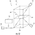
- FIG. 13 depicts an example temperature measurement system 150 for millisecond anneal system 200 .
- a simplified representation of the millisecond anneal system 200 is shown in FIG. 13 .
- the temperature of both sides of a semiconductor substrate 60 can be measured independently by temperature sensors, such as temperature sensor 152 and temperature sensor 154 .
- Temperature sensor 152 can measure a temperature of a top surface of the semiconductor substrate 60 .
- Temperature sensor 154 can measure a bottom surface of the semiconductor substrate 60 .
- narrow band pyrometric sensors with a measurement wavelength of about 1400 nm can be used as temperature sensors 152 and/or 154 to measure the temperature of, for instance, a center region of the semiconductor substrate 60 .
- the temperature sensors 152 and 154 can be ultra-fast radiometers (UFR) that have a sampling rate that is high enough to resolve the millisecond temperature spike cause by the flash heating.
- UFR ultra-fast radiometers
- the readings of the temperature sensors 152 and 154 can be emissivity compensated.
- the emissivity compensation scheme can include a diagnostic flash 156 , a reference temperature sensor 158 , and the temperature sensors 152 and 154 configured to measure the top and bottom surface of the semiconductor wafers. Diagnostic heating and measurements can be used with the diagnostic flash 156 (e.g., a test flash). Measurements from reference temperature sensor 158 can be used for emissivity compensation of temperature sensors 152 and 154 .
- the millisecond anneal system 200 can include water windows.
- the water windows can provide an optical filter that suppresses lamp radiation in the measurement band of the temperature sensors 152 and 154 so that the temperature sensors 152 and 154 only measure radiation from the semiconductor substrate.
- the readings of the temperature sensors 152 and 154 can be provided to a processor circuit 160 .
- the processor circuit 160 can be located within a housing of the millisecond anneal system 200 , although alternatively, the processor circuit 160 may be located remotely from the millisecond anneal system 200 .
- the various functions described herein may be performed by a single processor circuit if desired, or by other combinations of local and/or remote processor circuits.
- the readings of the temperature sensors 152 and 154 can be used by the processor circuit 160 to determine a temperature profile across the substrate.
- the temperature profile can provide a measure of the temperature of the substrate at various locations across the surface of the substrate.
- the temperature profile can provide a measure of thermal uniformity of the substrate during processing.
- data indicative of a temperature profile can be used for improving thermal uniformity by (1) changing the pressure inside the processing chamber of the millisecond anneal system; (2) manipulating the irradiation distribution by way of the refracting effect of a water window in the millisecond anneal system; (3) angular positioning of the wafer; and/or (4) configuring the shape of the reflectors used in the millisecond anneal system.
- the temperature uniformity of a semiconductor substrate can be improved during processing in a millisecond anneal system by changing the pressure inside the process chamber.
- the pressure inside the process chamber can influence a flow pattern of process gas inside the chamber, changing the convective cooling contribution on different regions of the wafer.
- the processing chamber in a millisecond anneal system can be operated at atmospheric pressure.
- the processing chamber can be sealed against the surrounding air to realize an ultra-pure gas ambient inside the chamber.
- the pressure inside the chamber can be modified within the limits given by the mechanical stability of the quartz plates of the water window.
- the allowable pressure range can be, for instance, about +2 kPa to about ⁇ 2 kPa pressure over atmosphere.
- a process for thermally treating a substrate in a millisecond anneal system can include obtaining data indicative of a temperature profile associated with one or more substrates during processing in a millisecond anneal system.
- a temperature profile can provide a measure of thermal uniformity of the substrate during processing.
- the temperature profile can provide a temperature at various points on the substrate.
- the data indicative of the temperature profile for one or more substrates can be analyzed to determine any non-uniformities in the temperature profile during process.
- a pressure in the processing chamber can be adjusted to affect the temperature uniformity across one or more substrates.
- the data indicative of the temperature profile can be obtained for a substrate during processing.
- Non-uniformities identified in the temperature profile can trigger the adjustment of the pressure during processing of the semiconductor substrate.
- a closed loop control of pressure based on the measured temperature profile can be used to adjust the temperature uniformity of a wafer during processing.
- FIG. 14 depicts an example gas flow system for adjusting pressure in the processing chamber 200 of a millisecond anneal system according to example embodiments of the present disclosure.
- the process chamber 200 can be an open flow system, where process gas is constantly entering the chamber from gas inlet 302 through gas inlet ports located in the top corners of the process chamber 200 .
- the process gas can leave the process chamber 200 chamber through vent ports located in the bottom corners of the process chambers. Downstream of the vent ports, the four vent lines can be combined to a single downstream line 304 .
- the downstream line 304 can be connected to a downstream exhaust duct 340 .
- the downstream duct 340 can provide a pressure differential PA relative to the process chamber 200 necessary to vent the process gas from the chamber 200 . By changing this pressure differential PA, the pressure in the processing chamber can be adjusted.
- the pressure differential PA can be adjusted by a controller 320 .
- the controller 320 can be any suitable control device, such as one or more processor circuits executing computer-readable instructions stored in one or more memory devices.
- a control variable for the controller 320 can be a pressure sensor 315 mounted to the chamber.
- the pressure sensor 315 can measure the pressure inside the chamber 200 and can send signals indicative of the pressure to the controller 320 over a suitable communication medium.
- the actuator of the controller 320 can be a valve 325 (e.g. a butterfly valve) in the vent manifold, changing the flow resistance and thus the pressure differential of the downstream line 304 .
- Low flow resistance can lower the chamber pressure.
- High flow resistance can increase the chamber pressure.
- the pressure set-point for the controller 320 can be defined by a user, for instance, based on a temperature profile across the substrate.
- the controller 320 can be configured to control the pressure based on signals from the pressure sensor to achieve the pressure-set point.
- the pressure differential can be adjusted by passive mechanical restrictions (e.g. orifices, dampers, or baffles) inside the vent line, or by setting the external exhaust duct pressure.
- the pressure inside the process chamber can influence a flow pattern of process gas inside the chamber.
- the convective cooling contribution on different regions of the wafer can be adjusted by adjusting the pressure inside the process chamber according to example embodiments of the present disclosure.
- Adjusting the pressure can also affect the irradiation distribution of lamp light provided through water windows in the millisecond anneal system.
- the temperature uniformity of a semiconductor substrate can be improved during processing in a millisecond anneal system by adjusting the irradiance distribution based on the refracting effect of a water window used in the millisecond anneal system.
- a water window in its normal state is a plane-parallel plate with a stack sequence of: (1) quartz; (2) water; (3) quartz. Water can flow through a sandwich of two quartz plates. Warping the stack can cause the water window to act as a lens for the lamp light passing through the window, adjusting the irradiation distribution through the water window.
- the warping of the water window can be accomplished by increasing or decreasing the pressure inside the chamber.
- the pressure inside the chamber can be modified within the limits given by the mechanical stability of the quartz plates of the water window.
- the allowable pressure range can be, for instance, about +2 kPa to about ⁇ 2 kPa pressure over atmosphere.
- a pressure change inside the chamber an affect the inner quartz plate of the water window. This can results in a thickness change of the water layer center to edge.
- FIGS. 15 and 16 illustrate a water window 260 having an inner plate 282 and an outer plate 284 .
- the inner plate 282 and the outer plate 284 can be formed from, for instance, quartz. Water can flow between the inner plate 282 and the outer plate 284 .
- the inner plate 282 can be disposed closer to the processing chamber of a millisecond anneal system relative to the outer plate 284 .
- the inner 282 of the water window 260 is bending outwards (e.g., away from the process chamber), resulting in a convex layer of water with a defocusing effect on light.
- the inner plate 282 of the water window 260 is bending inwards (e.g. toward the processing chamber), resulting in a convex layer of water with a focusing effect on light.
- the temperature uniformity of a patterned device wafer (e.g., a product wafer) during processing in a millisecond anneal system can be improved by angular wafer positioning.
- a product wafer can sometimes contain several hundreds of dies arranged in form of an array on the front surface of the wafer.
- FIG. 17 depicts an example product wafer 500 with devices in an array arrangement.
- the dies can be oriented along the main axis of the crystal lattice. Most commonly, the wafer surface is cut along the [100] plane of the silicon lattice. The wafer has a notch 502 marking the ⁇ 110> crystal lattice orientation.
- the die arrangement results in a laterally varying absorption ability of light. Hence the array of dies imposes a non-uniform light absorption property onto the wafer surface.
- FIG. 18 depicts a representation 510 of example residual non-uniformity of the irradiation of a wafer in a millisecond anneal system.
- the chamber can have a residual, inherent irradiation non-uniformity giving rise to a lateral wafer-temperature non-uniformity.
- This inherent irradiation non-uniformity can result, for instance, from the orientation of lamps, location of reflectors, and other components of the millisecond anneal system.
- Millisecond anneal systems can use a stationary, non-rotating wafer support arrangement. Therefore, the angular wafer orientation can be used to optimize or improve the temperature uniformity by aligning based at least in part on the irradiation pattern inherent to the chamber.
- a process for thermally treating a substrate in a millisecond anneal system can include obtaining data indicative of a temperature profile associated with one or more substrates during processing in a millisecond anneal system.
- the data indicative of the temperature profile for one or more substrates can be analyzed to determine any non-uniformities in the temperature profile during processing.
- the angular positioning of one or more wafers in the processing chamber can be adjusted to affect the temperature uniformity across the one or more substrates.
- FIG. 19 depicts a product wafer 500 located inside a processing chamber 200 .
- the wafer 500 can be placed at different angular orientations relative to the chamber and to the lamps.
- the wafer 500 is placed so that notch 502 is at notch alignment angle ⁇ . Accordingly, interaction between absorption pattern and irradiation pattern can be enhanced by adjusting the angular orientation of the wafer 500 .
- product wafers can be notch aligned before being loaded onto the handling system of the millisecond anneal system.
- the notch alignment angle ⁇ can determine the angular orientation inside the chamber. Wafer orientation can be measured based on the notch position relative to the chamber main axis (e.g., given by the walls).
- the notch alignment can be performed inside the processing chamber, for instance, by a notch alignment station or by a notch aligner integrated to a robot.
- wafers can be supported by quartz pins mounted to a wafer support plate.
- the number of pins used for supporting the wafer can vary between three up to six or more.
- a common wafer support scheme uses four pins arranged as a square with equal distance to the wafer center.
- the pins can cause a localized cold spot.
- the pins can induce a mechanical stress pattern.
- the negative impacts of the pins can be moved to more favorable regions of the wafer.
- wafer stress can be mitigated.
- FIG. 20 depicts a wafer 500 inside a processing chamber 200 with the location of support pins 212 relative the wafer 500 shown.
- Angular orientation of the wafer 500 relative to the pins 212 can reduce the influence of the pins 212 by positioning the pins 212 at different locations relative to the wafer 500 .
- the temperature uniformity of a semiconductor substrate can be improved during processing in a millisecond anneal system based at least in part the shape of one or more reflectors in the processing chamber of the millisecond anneal system.
- a top wedge reflector and/or one or more edge reflectors can have a shape and/or configuration designed to improve thermal uniformity.
- Small-sized reflectors can be used to reduce the residual non-uniformity of the processing chambers in millisecond anneal system.
- a process for thermally treating a substrate in a millisecond anneal system can include obtaining data indicative of a temperature profile associated with one or more substrates during processing in a millisecond anneal system.
- the data indicative of the temperature profile for one or more substrates can be analyzed to determine any non-uniformities in the temperature profile during process.
- the shape, configuration, and/or position of one or more reflectors in the processing chamber can be adjusted to affect the temperature uniformity across the one or more substrates.
- FIG. 21 depicts a cross sectional view of a millisecond anneal system showing the locations of top wedge reflectors 274 and edge reflectors 264 in a processing chamber in a millisecond anneal system.
- the top wedge reflectors 274 can be located on process chamber walls proximate the wafer plane plate.
- the top wedge reflectors 264 can be wedge shaped.
- the edge reflectors 264 can be located on the wafer plane plate and can surround a substrate during processing.
- top wedge reflectors 264 located on chamber walls in the top chamber portion of a processing chamber of a millisecond anneal system.
- the top edge reflectors 264 can be used to control the irradiation distribution perpendicular to the main axis of the lamps.
- the wedge reflectors 264 can be mounted in the top half of the chamber along the bottom edge of the mirror panels facing the door and facing the rear of the chamber.
- the wafer-temperature distribution has cold regions at the wafer edge, perpendicular to the lamp orientation.
- the size and magnitude of these cold spots can be impacted by the wedge reflectors 264 .
- Millisecond anneal systems can have the ability to trigger the flash discharge of each top lamp individually. The main application of this ability is to shape the time-temperature profile of the flash event.
- a side effect of this ability is that the irradiation pattern changes locally with time, as the top lamps are at different positions relative to the wafer. This can have impact on the size of the cold spot on the wafer edge, depending on the trigger sequence of the lamps. Using wedges with optimized angles can compensate for these effects.
- FIG. 22 depicts example top wedge reflectors 264 with varying wedge angles. More particularly, FIG. 22( a ) depicts a top wedge reflector 264 with a 0° wedge angle. FIG. 22( b ) depicts a top wedge reflector with a 10° wedge angle. By changing the wedge angle, the amount of light incident to the edge region can be controlled.
- the wedge reflectors 264 can be mounted to a motor or other mechanical apparatus that can be configured to adjust the position and/or wedge angle of the wedge reflectors 264 . For instance, a controller can adjust the wedge angle of the wedge reflectors in real time in response to temperature measurements of the substrate to provide for more uniform processing.
- the wedge angle can be pre-set by machining the parts. Optimization of the uniformity can be performed by mounting a suitable wedge with a selected wedge angle to the processing chamber. In another embodiment, the wedge angle can be set by inclining the wedge with shims, or by set screws. In some embodiments, the irradiation distribution is manipulated by additionally changing the wedge height and the wedge reflectivity.
- FIG. 23 depicts the example improvement of irradiation distribution by adjusting the wedge angle of the top wedge from a 5° wedge angle to a 1° wedge angle. More particularly, FIG. 23( a ) depicts a temperature profile of a wafer processed in a processing chamber having top wedge reflectors with a 5° wedge angle. As shown, the wafer can have cold spots 520 at the wafer edges due to reduced irradiance. FIG. 23( b ) depicts a temperature profile of a wafer processed in a processing chamber having top wedge reflectors with a 1° wedge angle. As shown, the temperature at the wafer edges 525 is more uniform and the presence of cold spots have been reduced.
- FIG. 24 depicts a perspective view of four edge reflectors 274 used in the processing chamber.
- the edge reflectors 274 can redirect light from the bottom lamps to the edge of the wafer.
- the reflectivity of the edge reflectors 274 can be modified by cutting slots 276 into the reflecting surface. The ratio of slot area to remaining reflector area determines the amount of reflectivity.
- FIG. 25 depicts a linear profile of a standard edge reflector 274 used in a millisecond anneal system.
- the temperature uniformity of a wafer can be modified by converting the profile shape from linear to parabolic, or a combination hereof, and/or by the relative position to the wafer. This determines the size and location of the heated zone on the wafer edge.
- FIG. 26( a ) depicts the reflection of light onto a substrate 60 by an edge reflector 274 with a linear profile 274 . 2 .
- FIG. 26( b ) depicts the reflection of light onto a substrate 60 by an edge reflector 274 with a combination of a parabolic and linear profile 274 . 4 .
- FIG. 26( c ) depicts the reflection of light onto substrate 60 by an edge reflector 274 with a combination of a parabolic and linear profile 274 . 4 but with an adjusted position relative to the substrate.
- the edge reflectors 274 can be mounted to a motor or other mechanical apparatus that can be configured to adjust the position and/or surface profile of the edge reflectors. For instance, a controller can adjust the position of one or more edge reflectors in real time in response to temperature measurements of the substrate to provide for more uniform processing.
Landscapes
- Engineering & Computer Science (AREA)
- Physics & Mathematics (AREA)
- Manufacturing & Machinery (AREA)
- Microelectronics & Electronic Packaging (AREA)
- General Physics & Mathematics (AREA)
- Computer Hardware Design (AREA)
- Condensed Matter Physics & Semiconductors (AREA)
- Power Engineering (AREA)
- High Energy & Nuclear Physics (AREA)
- Health & Medical Sciences (AREA)
- Toxicology (AREA)
- Electromagnetism (AREA)
- Optics & Photonics (AREA)
- Container, Conveyance, Adherence, Positioning, Of Wafer (AREA)
- Recrystallisation Techniques (AREA)
Abstract
Description
Claims (10)
Priority Applications (2)
| Application Number | Priority Date | Filing Date | Title |
|---|---|---|---|
| US15/378,580 US10770309B2 (en) | 2015-12-30 | 2016-12-14 | Features for improving process uniformity in a millisecond anneal system |
| US17/012,146 US20200402811A1 (en) | 2015-12-30 | 2020-09-04 | Features for Improving Process Uniformity in a Millisecond Anneal System |
Applications Claiming Priority (2)
| Application Number | Priority Date | Filing Date | Title |
|---|---|---|---|
| US201562272817P | 2015-12-30 | 2015-12-30 | |
| US15/378,580 US10770309B2 (en) | 2015-12-30 | 2016-12-14 | Features for improving process uniformity in a millisecond anneal system |
Related Child Applications (1)
| Application Number | Title | Priority Date | Filing Date |
|---|---|---|---|
| US17/012,146 Division US20200402811A1 (en) | 2015-12-30 | 2020-09-04 | Features for Improving Process Uniformity in a Millisecond Anneal System |
Publications (2)
| Publication Number | Publication Date |
|---|---|
| US20170194163A1 US20170194163A1 (en) | 2017-07-06 |
| US10770309B2 true US10770309B2 (en) | 2020-09-08 |
Family
ID=59225810
Family Applications (2)
| Application Number | Title | Priority Date | Filing Date |
|---|---|---|---|
| US15/378,580 Active 2039-01-28 US10770309B2 (en) | 2015-12-30 | 2016-12-14 | Features for improving process uniformity in a millisecond anneal system |
| US17/012,146 Abandoned US20200402811A1 (en) | 2015-12-30 | 2020-09-04 | Features for Improving Process Uniformity in a Millisecond Anneal System |
Family Applications After (1)
| Application Number | Title | Priority Date | Filing Date |
|---|---|---|---|
| US17/012,146 Abandoned US20200402811A1 (en) | 2015-12-30 | 2020-09-04 | Features for Improving Process Uniformity in a Millisecond Anneal System |
Country Status (5)
| Country | Link |
|---|---|
| US (2) | US10770309B2 (en) |
| KR (1) | KR102104468B1 (en) |
| CN (1) | CN108028200B (en) |
| TW (1) | TWI753873B (en) |
| WO (1) | WO2017116708A1 (en) |
Cited By (1)
| Publication number | Priority date | Publication date | Assignee | Title |
|---|---|---|---|---|
| CN112274143A (en) * | 2020-12-29 | 2021-01-29 | 四川写正智能科技有限公司 | Human body existing state detection method and detection device |
Families Citing this family (5)
| Publication number | Priority date | Publication date | Assignee | Title |
|---|---|---|---|---|
| US10840114B1 (en) * | 2016-07-26 | 2020-11-17 | Raytheon Company | Rapid thermal anneal apparatus and method |
| CN109496365B (en) * | 2017-01-26 | 2023-03-24 | L·K·格罗斯 | Method and device for separating different material layers of a composite component |
| US20210043478A1 (en) * | 2019-08-07 | 2021-02-11 | Samsung Electronics Co., Ltd. | Pressure heating apparatus |
| KR20210083411A (en) * | 2019-12-26 | 2021-07-07 | 삼성디스플레이 주식회사 | Glass substrate chemical strengthening furnace device |
| CN111755364B (en) * | 2020-08-13 | 2023-04-07 | 抚州华成半导体科技有限公司 | Semiconductor diode production equipment |
Citations (23)
| Publication number | Priority date | Publication date | Assignee | Title |
|---|---|---|---|---|
| US6114216A (en) * | 1996-11-13 | 2000-09-05 | Applied Materials, Inc. | Methods for shallow trench isolation |
| US6204203B1 (en) | 1998-10-14 | 2001-03-20 | Applied Materials, Inc. | Post deposition treatment of dielectric films for interface control |
| WO2002005323A2 (en) | 2000-07-06 | 2002-01-17 | Applied Materials, Inc. | Thermally processing a substrate |
| US20040058560A1 (en) * | 2002-09-20 | 2004-03-25 | Applied Materials, Inc. | Fast gas exchange for thermal conductivity modulation |
| US20050172904A1 (en) | 1998-07-16 | 2005-08-11 | Tokyo Electron At Limited And Japan Science And Technology Corporation | Plasma processing apparatus and plasma processing method |
| US7442415B2 (en) | 2003-04-11 | 2008-10-28 | Sharp Laboratories Of America, Inc. | Modulated temperature method of atomic layer deposition (ALD) of high dielectric constant films |
| US20090114158A1 (en) * | 2007-11-07 | 2009-05-07 | Mattson Technology, Inc. | Workpiece Support With Fluid Zones For Temperature Control |
| JP2009123810A (en) | 2007-11-13 | 2009-06-04 | Dainippon Screen Mfg Co Ltd | Heat treatment apparatus |
| US20090175606A1 (en) | 2008-01-08 | 2009-07-09 | International Business Machines Corporation | Method and structure to control thermal gradients in semiconductor wafers during rapid thermal processing |
| US20090175605A1 (en) | 2008-01-09 | 2009-07-09 | Ippei Kobayashi | Heat treatment apparatus for heating substrate by exposing substrate to flash light |
| US7790633B1 (en) | 2004-10-26 | 2010-09-07 | Novellus Systems, Inc. | Sequential deposition/anneal film densification method |
| US20110034015A1 (en) | 2009-08-10 | 2011-02-10 | Kabushiki Kaisha Toshiba | Heat treatment apparatus and method for manufacturing semiconductor device |
| US20110081137A1 (en) | 2009-10-06 | 2011-04-07 | Advantest Corporation | Manufacturing equipment and manufacturing method |
| US20110312156A1 (en) * | 2008-03-28 | 2011-12-22 | S.O.I. Tec Silicon On Insulator Technologies | Controlled temperature implantation |
| US20120088194A1 (en) * | 2007-06-12 | 2012-04-12 | Fujifilm Corporation | Method of forming patterns |
| US8323754B2 (en) | 2004-05-21 | 2012-12-04 | Applied Materials, Inc. | Stabilization of high-k dielectric materials |
| US20140169772A1 (en) | 2012-12-13 | 2014-06-19 | Dainippon Screen Mfg. Co., Ltd. | Heat treatment apparatus for heating substrate by irradiation with flash light |
| US20140199056A1 (en) * | 2013-01-16 | 2014-07-17 | Applied Materials, Inc. | Quartz upper and lower domes |
| US8809175B2 (en) | 2011-07-15 | 2014-08-19 | Taiwan Semiconductor Manufacturing Company, Ltd. | Methods of anneal after deposition of gate layers |
| JP2014175638A (en) | 2013-03-13 | 2014-09-22 | Dainippon Screen Mfg Co Ltd | Heat treatment equipment and heat treatment method |
| US20150140838A1 (en) | 2013-11-19 | 2015-05-21 | Intermolecular Inc. | Two Step Deposition of High-k Gate Dielectric Materials |
| US9093468B2 (en) | 2013-03-13 | 2015-07-28 | Taiwan Semiconductor Manufacturing Company, Ltd. | Asymmetric cyclic depositon and etch process for epitaxial formation mechanisms of source and drain regions |
| US20170194177A1 (en) * | 2015-12-30 | 2017-07-06 | Mattson Technology, Inc. | Substrate Breakage Detection in a Thermal Processing System |
Family Cites Families (15)
| Publication number | Priority date | Publication date | Assignee | Title |
|---|---|---|---|---|
| US6771895B2 (en) * | 1999-01-06 | 2004-08-03 | Mattson Technology, Inc. | Heating device for heating semiconductor wafers in thermal processing chambers |
| US6594446B2 (en) * | 2000-12-04 | 2003-07-15 | Vortek Industries Ltd. | Heat-treating methods and systems |
| KR101067901B1 (en) * | 2001-12-26 | 2011-09-28 | 맷슨 테크날러지 캐나다 인코퍼레이티드 | Temperature measurement and heat-treating methods and systems |
| CN101702950B (en) * | 2007-05-01 | 2012-05-30 | 加拿大马特森技术有限公司 | Irradiance pulse heat-treating methods and apparatus |
| US9498845B2 (en) * | 2007-11-08 | 2016-11-22 | Applied Materials, Inc. | Pulse train annealing method and apparatus |
| US7800081B2 (en) * | 2007-11-08 | 2010-09-21 | Applied Materials, Inc. | Pulse train annealing method and apparatus |
| US8548311B2 (en) * | 2008-04-09 | 2013-10-01 | Applied Materials, Inc. | Apparatus and method for improved control of heating and cooling of substrates |
| US20100068898A1 (en) * | 2008-09-17 | 2010-03-18 | Stephen Moffatt | Managing thermal budget in annealing of substrates |
| US8383513B2 (en) * | 2010-10-05 | 2013-02-26 | Taiwan Semiconductor Manufacturing Company, Ltd. | Asymmetric rapid thermal annealing to reduce pattern effect |
| US10388493B2 (en) * | 2011-09-16 | 2019-08-20 | Lam Research Corporation | Component of a substrate support assembly producing localized magnetic fields |
| JP2016529733A (en) * | 2013-08-30 | 2016-09-23 | アプライド マテリアルズ インコーポレイテッドApplied Materials,Incorporated | Substrate support system |
| CN108369918B (en) * | 2015-12-30 | 2021-12-24 | 玛特森技术公司 | Nitrogen injection for arc lamps |
| US9892956B1 (en) * | 2016-10-12 | 2018-02-13 | Lam Research Corporation | Wafer positioning pedestal for semiconductor processing |
| GB201706284D0 (en) * | 2017-04-20 | 2017-06-07 | Spts Technologies Ltd | A method and apparatus for controlling stress variation in a material layer formed via pulsed DC physical vapour deposition |
| US20210109450A1 (en) * | 2019-10-11 | 2021-04-15 | Tokyo Electron Limited | Apparatus and Methods for Beam Processing of Substrates |
-
2016
- 2016-12-14 WO PCT/US2016/066561 patent/WO2017116708A1/en active Application Filing
- 2016-12-14 US US15/378,580 patent/US10770309B2/en active Active
- 2016-12-14 KR KR1020187006723A patent/KR102104468B1/en active IP Right Grant
- 2016-12-14 CN CN201680054608.XA patent/CN108028200B/en active Active
- 2016-12-21 TW TW105142449A patent/TWI753873B/en active
-
2020
- 2020-09-04 US US17/012,146 patent/US20200402811A1/en not_active Abandoned
Patent Citations (23)
| Publication number | Priority date | Publication date | Assignee | Title |
|---|---|---|---|---|
| US6114216A (en) * | 1996-11-13 | 2000-09-05 | Applied Materials, Inc. | Methods for shallow trench isolation |
| US20050172904A1 (en) | 1998-07-16 | 2005-08-11 | Tokyo Electron At Limited And Japan Science And Technology Corporation | Plasma processing apparatus and plasma processing method |
| US6204203B1 (en) | 1998-10-14 | 2001-03-20 | Applied Materials, Inc. | Post deposition treatment of dielectric films for interface control |
| WO2002005323A2 (en) | 2000-07-06 | 2002-01-17 | Applied Materials, Inc. | Thermally processing a substrate |
| US20040058560A1 (en) * | 2002-09-20 | 2004-03-25 | Applied Materials, Inc. | Fast gas exchange for thermal conductivity modulation |
| US7442415B2 (en) | 2003-04-11 | 2008-10-28 | Sharp Laboratories Of America, Inc. | Modulated temperature method of atomic layer deposition (ALD) of high dielectric constant films |
| US8323754B2 (en) | 2004-05-21 | 2012-12-04 | Applied Materials, Inc. | Stabilization of high-k dielectric materials |
| US7790633B1 (en) | 2004-10-26 | 2010-09-07 | Novellus Systems, Inc. | Sequential deposition/anneal film densification method |
| US20120088194A1 (en) * | 2007-06-12 | 2012-04-12 | Fujifilm Corporation | Method of forming patterns |
| US20090114158A1 (en) * | 2007-11-07 | 2009-05-07 | Mattson Technology, Inc. | Workpiece Support With Fluid Zones For Temperature Control |
| JP2009123810A (en) | 2007-11-13 | 2009-06-04 | Dainippon Screen Mfg Co Ltd | Heat treatment apparatus |
| US20090175606A1 (en) | 2008-01-08 | 2009-07-09 | International Business Machines Corporation | Method and structure to control thermal gradients in semiconductor wafers during rapid thermal processing |
| US20090175605A1 (en) | 2008-01-09 | 2009-07-09 | Ippei Kobayashi | Heat treatment apparatus for heating substrate by exposing substrate to flash light |
| US20110312156A1 (en) * | 2008-03-28 | 2011-12-22 | S.O.I. Tec Silicon On Insulator Technologies | Controlled temperature implantation |
| US20110034015A1 (en) | 2009-08-10 | 2011-02-10 | Kabushiki Kaisha Toshiba | Heat treatment apparatus and method for manufacturing semiconductor device |
| US20110081137A1 (en) | 2009-10-06 | 2011-04-07 | Advantest Corporation | Manufacturing equipment and manufacturing method |
| US8809175B2 (en) | 2011-07-15 | 2014-08-19 | Taiwan Semiconductor Manufacturing Company, Ltd. | Methods of anneal after deposition of gate layers |
| US20140169772A1 (en) | 2012-12-13 | 2014-06-19 | Dainippon Screen Mfg. Co., Ltd. | Heat treatment apparatus for heating substrate by irradiation with flash light |
| US20140199056A1 (en) * | 2013-01-16 | 2014-07-17 | Applied Materials, Inc. | Quartz upper and lower domes |
| JP2014175638A (en) | 2013-03-13 | 2014-09-22 | Dainippon Screen Mfg Co Ltd | Heat treatment equipment and heat treatment method |
| US9093468B2 (en) | 2013-03-13 | 2015-07-28 | Taiwan Semiconductor Manufacturing Company, Ltd. | Asymmetric cyclic depositon and etch process for epitaxial formation mechanisms of source and drain regions |
| US20150140838A1 (en) | 2013-11-19 | 2015-05-21 | Intermolecular Inc. | Two Step Deposition of High-k Gate Dielectric Materials |
| US20170194177A1 (en) * | 2015-12-30 | 2017-07-06 | Mattson Technology, Inc. | Substrate Breakage Detection in a Thermal Processing System |
Non-Patent Citations (12)
| Title |
|---|
| Conley, Jr. et al., "Densification and improved electrical properties of pulse-deposited films via in situ modulated temperature annealing," Applied Physics Letters, vol. 84, Issue 11, Mar. 15, 2004, pp. 1913-1915. |
| Driemeier et al., "Room temperature interactions of water vapor with Hf O2 films on Si," Applied Physics Letters, vol. 88, Issue 20, May 2006-3 pages. |
| Driemeier et al., "Thermochemical behavior of hydrogen in hafnium silicate films on Si," Applied Physics Letters, vol. 89, Issue 5, Aug. 2006,-4 pages. |
| Driemeier et al., "Room temperature interactions of water vapor with Hf O2 films on Si," Applied Physics Letters, vol. 88, Issue 20, May 2006—3 pages. |
| Driemeier et al., "Thermochemical behavior of hydrogen in hafnium silicate films on Si," Applied Physics Letters, vol. 89, Issue 5, Aug. 2006,—4 pages. |
| Ferrari et al., "Diffusion Reaction of Oxygen in HfO2/SiO2/Si Stacks," The Journal of Physical Chemistry B, vol. 110, No. 30, Jul. 12, 2006, pp. 14905-14910. |
| Nakajima et al., "Experimental Demonstration of Higher-k phase HfO2 through Non-equilibrium Thermal Treatment," ECS Transactions 28.2 (2010), pp. 203-212. |
| PCT International Preliminary Report on Patentability for corresponding PCT Application No. PCT/US2016/066561, dated Jul. 12, 2018-9 pages. |
| PCT International Preliminary Report on Patentability for corresponding PCT Application No. PCT/US2016/066561, dated Jul. 12, 2018—9 pages. |
| PCT International Search Report for corresponding PCT Application No. PCT/US2016/066561, dated Mar. 29, 2017, 3 pages. |
| Ragnarsson et al., "The Importance of Moisture Control for EOT Scaling of Hf-Based Dielectrics," Journal of the Electrochemical Society, vol. 156, Issue 6, Apr. 3, 2009, pp. H416-H423. |
| Wu et al., "Device Performance and Reliability Improvement for MOSFETs With HfO2 Gate Dielectrics Fabricated Using Multideposition Room-Temperature Multiannealing," IEEE Electron Device Letters, vol. 32, Issue 9, Sep. 2011, pp. 1173-1175. |
Cited By (2)
| Publication number | Priority date | Publication date | Assignee | Title |
|---|---|---|---|---|
| CN112274143A (en) * | 2020-12-29 | 2021-01-29 | 四川写正智能科技有限公司 | Human body existing state detection method and detection device |
| CN112274143B (en) * | 2020-12-29 | 2021-06-01 | 四川写正智能科技有限公司 | Human body existing state detection method and detection device |
Also Published As
| Publication number | Publication date |
|---|---|
| US20170194163A1 (en) | 2017-07-06 |
| TWI753873B (en) | 2022-02-01 |
| US20200402811A1 (en) | 2020-12-24 |
| CN108028200A (en) | 2018-05-11 |
| WO2017116708A1 (en) | 2017-07-06 |
| KR20180030232A (en) | 2018-03-21 |
| CN108028200B (en) | 2022-05-27 |
| KR102104468B1 (en) | 2020-04-27 |
| TW201727751A (en) | 2017-08-01 |
Similar Documents
| Publication | Publication Date | Title |
|---|---|---|
| US20200402811A1 (en) | Features for Improving Process Uniformity in a Millisecond Anneal System | |
| US12027427B2 (en) | Preheat processes for millisecond anneal system | |
| CN108352344B (en) | Fluid leak detection for millisecond anneal systems | |
| KR102148834B1 (en) | Gas flow control for millisecond annealing systems | |
| US10957563B2 (en) | Chamber wall heating for a millisecond anneal system | |
| KR102155100B1 (en) | Electrode tip for arc lamp |
Legal Events
| Date | Code | Title | Description |
|---|---|---|---|
| AS | Assignment |
Owner name: MATTSON THERMAL PRODUCTS GMBH, GERMANY Free format text: ASSIGNMENT OF ASSIGNORS INTEREST;ASSIGNORS:COSCEEV, ALEXANDR;HAGEDORN, MARKUS;PFAHLER, CHRISTIAN;SIGNING DATES FROM 20160524 TO 20160531;REEL/FRAME:040733/0976 Owner name: MATTSON TECHNOLOGY, INC., CALIFORNIA Free format text: ASSIGNMENT OF ASSIGNORS INTEREST;ASSIGNOR:MATTSON THERMAL PRODUCTS GMBH;REEL/FRAME:040734/0089 Effective date: 20161004 |
|
| STPP | Information on status: patent application and granting procedure in general |
Free format text: DOCKETED NEW CASE - READY FOR EXAMINATION |
|
| AS | Assignment |
Owner name: EAST WEST BANK, CALIFORNIA Free format text: SECURITY INTEREST;ASSIGNOR:MATTSON TECHNOLOGY, INC.;REEL/FRAME:046956/0348 Effective date: 20180821 |
|
| STPP | Information on status: patent application and granting procedure in general |
Free format text: NON FINAL ACTION MAILED |
|
| AS | Assignment |
Owner name: MATTSON TECHNOLOGY, INC., CALIFORNIA Free format text: ASSIGNMENT OF ASSIGNORS INTEREST;ASSIGNOR:MATTSON TECHNOLOGY, INC.;REEL/FRAME:050582/0796 Effective date: 20190925 Owner name: BEIJING E-TOWN SEMICONDUCTOR TECHNOLOGY, CO., LTD, Free format text: ASSIGNMENT OF ASSIGNORS INTEREST;ASSIGNOR:MATTSON TECHNOLOGY, INC.;REEL/FRAME:050582/0796 Effective date: 20190925 Owner name: BEIJING E-TOWN SEMICONDUCTOR TECHNOLOGY, CO., LTD, CHINA Free format text: ASSIGNMENT OF ASSIGNORS INTEREST;ASSIGNOR:MATTSON TECHNOLOGY, INC.;REEL/FRAME:050582/0796 Effective date: 20190925 |
|
| STPP | Information on status: patent application and granting procedure in general |
Free format text: NON FINAL ACTION MAILED |
|
| STPP | Information on status: patent application and granting procedure in general |
Free format text: RESPONSE TO NON-FINAL OFFICE ACTION ENTERED AND FORWARDED TO EXAMINER |
|
| STPP | Information on status: patent application and granting procedure in general |
Free format text: PUBLICATIONS -- ISSUE FEE PAYMENT RECEIVED |
|
| STCF | Information on status: patent grant |
Free format text: PATENTED CASE |
|
| AS | Assignment |
Owner name: EAST WEST BANK, CALIFORNIA Free format text: SECURITY INTEREST;ASSIGNOR:MATTSON TECHNOLOGY, INC.;REEL/FRAME:054100/0167 Effective date: 20180821 |
|
| AS | Assignment |
Owner name: MATTSON TECHNOLOGY, INC., CALIFORNIA Free format text: RELEASE BY SECURED PARTY;ASSIGNOR:EAST WEST BANK;REEL/FRAME:055950/0452 Effective date: 20210415 |
|
| MAFP | Maintenance fee payment |
Free format text: PAYMENT OF MAINTENANCE FEE, 4TH YEAR, LARGE ENTITY (ORIGINAL EVENT CODE: M1551); ENTITY STATUS OF PATENT OWNER: LARGE ENTITY Year of fee payment: 4 |