JP2016529733A - Substrate support system - Google Patents
Substrate support system Download PDFInfo
- Publication number
- JP2016529733A JP2016529733A JP2016538940A JP2016538940A JP2016529733A JP 2016529733 A JP2016529733 A JP 2016529733A JP 2016538940 A JP2016538940 A JP 2016538940A JP 2016538940 A JP2016538940 A JP 2016538940A JP 2016529733 A JP2016529733 A JP 2016529733A
- Authority
- JP
- Japan
- Prior art keywords
- substrate
- pedestal
- processing chamber
- end support
- support member
- Prior art date
- Legal status (The legal status is an assumption and is not a legal conclusion. Google has not performed a legal analysis and makes no representation as to the accuracy of the status listed.)
- Pending
Links
Images


Classifications
-
- H—ELECTRICITY
- H01—ELECTRIC ELEMENTS
- H01L—SEMICONDUCTOR DEVICES NOT COVERED BY CLASS H10
- H01L21/00—Processes or apparatus adapted for the manufacture or treatment of semiconductor or solid state devices or of parts thereof
- H01L21/67—Apparatus specially adapted for handling semiconductor or electric solid state devices during manufacture or treatment thereof; Apparatus specially adapted for handling wafers during manufacture or treatment of semiconductor or electric solid state devices or components ; Apparatus not specifically provided for elsewhere
- H01L21/683—Apparatus specially adapted for handling semiconductor or electric solid state devices during manufacture or treatment thereof; Apparatus specially adapted for handling wafers during manufacture or treatment of semiconductor or electric solid state devices or components ; Apparatus not specifically provided for elsewhere for supporting or gripping
- H01L21/687—Apparatus specially adapted for handling semiconductor or electric solid state devices during manufacture or treatment thereof; Apparatus specially adapted for handling wafers during manufacture or treatment of semiconductor or electric solid state devices or components ; Apparatus not specifically provided for elsewhere for supporting or gripping using mechanical means, e.g. chucks, clamps or pinches
- H01L21/68714—Apparatus specially adapted for handling semiconductor or electric solid state devices during manufacture or treatment thereof; Apparatus specially adapted for handling wafers during manufacture or treatment of semiconductor or electric solid state devices or components ; Apparatus not specifically provided for elsewhere for supporting or gripping using mechanical means, e.g. chucks, clamps or pinches the wafers being placed on a susceptor, stage or support
- H01L21/68742—Apparatus specially adapted for handling semiconductor or electric solid state devices during manufacture or treatment thereof; Apparatus specially adapted for handling wafers during manufacture or treatment of semiconductor or electric solid state devices or components ; Apparatus not specifically provided for elsewhere for supporting or gripping using mechanical means, e.g. chucks, clamps or pinches the wafers being placed on a susceptor, stage or support characterised by a lifting arrangement, e.g. lift pins
-
- H—ELECTRICITY
- H01—ELECTRIC ELEMENTS
- H01L—SEMICONDUCTOR DEVICES NOT COVERED BY CLASS H10
- H01L21/00—Processes or apparatus adapted for the manufacture or treatment of semiconductor or solid state devices or of parts thereof
- H01L21/67—Apparatus specially adapted for handling semiconductor or electric solid state devices during manufacture or treatment thereof; Apparatus specially adapted for handling wafers during manufacture or treatment of semiconductor or electric solid state devices or components ; Apparatus not specifically provided for elsewhere
- H01L21/683—Apparatus specially adapted for handling semiconductor or electric solid state devices during manufacture or treatment thereof; Apparatus specially adapted for handling wafers during manufacture or treatment of semiconductor or electric solid state devices or components ; Apparatus not specifically provided for elsewhere for supporting or gripping
- H01L21/687—Apparatus specially adapted for handling semiconductor or electric solid state devices during manufacture or treatment thereof; Apparatus specially adapted for handling wafers during manufacture or treatment of semiconductor or electric solid state devices or components ; Apparatus not specifically provided for elsewhere for supporting or gripping using mechanical means, e.g. chucks, clamps or pinches
- H01L21/68714—Apparatus specially adapted for handling semiconductor or electric solid state devices during manufacture or treatment thereof; Apparatus specially adapted for handling wafers during manufacture or treatment of semiconductor or electric solid state devices or components ; Apparatus not specifically provided for elsewhere for supporting or gripping using mechanical means, e.g. chucks, clamps or pinches the wafers being placed on a susceptor, stage or support
- H01L21/68735—Apparatus specially adapted for handling semiconductor or electric solid state devices during manufacture or treatment thereof; Apparatus specially adapted for handling wafers during manufacture or treatment of semiconductor or electric solid state devices or components ; Apparatus not specifically provided for elsewhere for supporting or gripping using mechanical means, e.g. chucks, clamps or pinches the wafers being placed on a susceptor, stage or support characterised by edge profile or support profile
-
- H—ELECTRICITY
- H01—ELECTRIC ELEMENTS
- H01L—SEMICONDUCTOR DEVICES NOT COVERED BY CLASS H10
- H01L21/00—Processes or apparatus adapted for the manufacture or treatment of semiconductor or solid state devices or of parts thereof
- H01L21/67—Apparatus specially adapted for handling semiconductor or electric solid state devices during manufacture or treatment thereof; Apparatus specially adapted for handling wafers during manufacture or treatment of semiconductor or electric solid state devices or components ; Apparatus not specifically provided for elsewhere
- H01L21/683—Apparatus specially adapted for handling semiconductor or electric solid state devices during manufacture or treatment thereof; Apparatus specially adapted for handling wafers during manufacture or treatment of semiconductor or electric solid state devices or components ; Apparatus not specifically provided for elsewhere for supporting or gripping
- H01L21/687—Apparatus specially adapted for handling semiconductor or electric solid state devices during manufacture or treatment thereof; Apparatus specially adapted for handling wafers during manufacture or treatment of semiconductor or electric solid state devices or components ; Apparatus not specifically provided for elsewhere for supporting or gripping using mechanical means, e.g. chucks, clamps or pinches
- H01L21/68714—Apparatus specially adapted for handling semiconductor or electric solid state devices during manufacture or treatment thereof; Apparatus specially adapted for handling wafers during manufacture or treatment of semiconductor or electric solid state devices or components ; Apparatus not specifically provided for elsewhere for supporting or gripping using mechanical means, e.g. chucks, clamps or pinches the wafers being placed on a susceptor, stage or support
- H01L21/68764—Apparatus specially adapted for handling semiconductor or electric solid state devices during manufacture or treatment thereof; Apparatus specially adapted for handling wafers during manufacture or treatment of semiconductor or electric solid state devices or components ; Apparatus not specifically provided for elsewhere for supporting or gripping using mechanical means, e.g. chucks, clamps or pinches the wafers being placed on a susceptor, stage or support characterised by a movable susceptor, stage or support, others than those only rotating on their own vertical axis, e.g. susceptors on a rotating caroussel
-
- H—ELECTRICITY
- H01—ELECTRIC ELEMENTS
- H01L—SEMICONDUCTOR DEVICES NOT COVERED BY CLASS H10
- H01L21/00—Processes or apparatus adapted for the manufacture or treatment of semiconductor or solid state devices or of parts thereof
- H01L21/67—Apparatus specially adapted for handling semiconductor or electric solid state devices during manufacture or treatment thereof; Apparatus specially adapted for handling wafers during manufacture or treatment of semiconductor or electric solid state devices or components ; Apparatus not specifically provided for elsewhere
- H01L21/683—Apparatus specially adapted for handling semiconductor or electric solid state devices during manufacture or treatment thereof; Apparatus specially adapted for handling wafers during manufacture or treatment of semiconductor or electric solid state devices or components ; Apparatus not specifically provided for elsewhere for supporting or gripping
- H01L21/687—Apparatus specially adapted for handling semiconductor or electric solid state devices during manufacture or treatment thereof; Apparatus specially adapted for handling wafers during manufacture or treatment of semiconductor or electric solid state devices or components ; Apparatus not specifically provided for elsewhere for supporting or gripping using mechanical means, e.g. chucks, clamps or pinches
- H01L21/68714—Apparatus specially adapted for handling semiconductor or electric solid state devices during manufacture or treatment thereof; Apparatus specially adapted for handling wafers during manufacture or treatment of semiconductor or electric solid state devices or components ; Apparatus not specifically provided for elsewhere for supporting or gripping using mechanical means, e.g. chucks, clamps or pinches the wafers being placed on a susceptor, stage or support
- H01L21/68785—Apparatus specially adapted for handling semiconductor or electric solid state devices during manufacture or treatment thereof; Apparatus specially adapted for handling wafers during manufacture or treatment of semiconductor or electric solid state devices or components ; Apparatus not specifically provided for elsewhere for supporting or gripping using mechanical means, e.g. chucks, clamps or pinches the wafers being placed on a susceptor, stage or support characterised by the mechanical construction of the susceptor, stage or support
-
- H—ELECTRICITY
- H01—ELECTRIC ELEMENTS
- H01L—SEMICONDUCTOR DEVICES NOT COVERED BY CLASS H10
- H01L21/00—Processes or apparatus adapted for the manufacture or treatment of semiconductor or solid state devices or of parts thereof
- H01L21/67—Apparatus specially adapted for handling semiconductor or electric solid state devices during manufacture or treatment thereof; Apparatus specially adapted for handling wafers during manufacture or treatment of semiconductor or electric solid state devices or components ; Apparatus not specifically provided for elsewhere
- H01L21/683—Apparatus specially adapted for handling semiconductor or electric solid state devices during manufacture or treatment thereof; Apparatus specially adapted for handling wafers during manufacture or treatment of semiconductor or electric solid state devices or components ; Apparatus not specifically provided for elsewhere for supporting or gripping
- H01L21/687—Apparatus specially adapted for handling semiconductor or electric solid state devices during manufacture or treatment thereof; Apparatus specially adapted for handling wafers during manufacture or treatment of semiconductor or electric solid state devices or components ; Apparatus not specifically provided for elsewhere for supporting or gripping using mechanical means, e.g. chucks, clamps or pinches
- H01L21/68714—Apparatus specially adapted for handling semiconductor or electric solid state devices during manufacture or treatment thereof; Apparatus specially adapted for handling wafers during manufacture or treatment of semiconductor or electric solid state devices or components ; Apparatus not specifically provided for elsewhere for supporting or gripping using mechanical means, e.g. chucks, clamps or pinches the wafers being placed on a susceptor, stage or support
- H01L21/68792—Apparatus specially adapted for handling semiconductor or electric solid state devices during manufacture or treatment thereof; Apparatus specially adapted for handling wafers during manufacture or treatment of semiconductor or electric solid state devices or components ; Apparatus not specifically provided for elsewhere for supporting or gripping using mechanical means, e.g. chucks, clamps or pinches the wafers being placed on a susceptor, stage or support characterised by the construction of the shaft
Abstract
基板処理チャンバ用の基板支持システムのための方法及び装置であって、チャンバは、処理領域を囲むチャンバ本体、処理領域内に少なくとも部分的に配置される第1の基板支持体及び第2の基板支持体を備え、第2の基板支持体は第1の基板支持体を取り囲み、第1の基板支持体及び第2の基板支持体のうちの片方又は両方は互いに対して可動であり、且つ第1の基板支持体は第2の基板支持体に対して回転可能である、基板支持システムのための方法及び装置。【選択図】図1A method and apparatus for a substrate support system for a substrate processing chamber, the chamber comprising a chamber body surrounding a processing region, a first substrate support and a second substrate disposed at least partially within the processing region. And a second substrate support surrounds the first substrate support, one or both of the first substrate support and the second substrate support being movable relative to each other, and the first substrate support. A method and apparatus for a substrate support system, wherein one substrate support is rotatable relative to a second substrate support. [Selection] Figure 1
Description
[0001]本開示の実施形態は、概して処理チャンバのための基板支持システムに関する。より具体的には、本明細書に記載された実施形態は、基板支持システムを使用して、ペデスタルに対して基板を移動させること、或いは、基板に対してペデスタルを移動させることのうちの1つ又はそれらの組み合わせによって、基板上で測定された不均一を平均化し得る(すなわち、平均により近づける)基板支持システムに関する。 [0001] Embodiments of the present disclosure generally relate to a substrate support system for a processing chamber. More specifically, the embodiments described herein use a substrate support system to move the substrate relative to the pedestal or one of moving the pedestal relative to the substrate. One or a combination thereof relates to a substrate support system that can average (ie, bring closer to the average) non-uniformities measured on the substrate.
[0002]集積回路は、単一のチップ上に数百万もの部品(例えば、トランジスタ、キャパシタ、及びレジスタなど)を含み得る複雑な装置へと進化してきた。チップ設計の進化には、より迅速な回路及びより高い回路密度が継続的に必要とされる。回路密度をより高くする需要は、集積回路部品の寸法の縮小を余儀なくする。このような装置の特徴の最小寸法は、当該技術で一般的に限界寸法と呼ばれる。限界寸法には、概して、ライン、コラム、開口部、ライン間の隙間、及び装置/膜の厚みなどの特徴の最小寸法が含まれる。これらの限界寸法が縮小するにつれて、測定及び処理を正確に制御することがより難しくなる。 [0002] Integrated circuits have evolved into complex devices that can include millions of components (eg, transistors, capacitors, resistors, etc.) on a single chip. The evolution of chip design continually requires faster circuits and higher circuit densities. The demand for higher circuit density necessitates a reduction in the dimensions of integrated circuit components. The minimum dimension of such device features is commonly referred to in the art as the critical dimension. Critical dimensions generally include minimum dimensions of features such as lines, columns, openings, gaps between lines, and device / membrane thickness. As these critical dimensions shrink, it becomes more difficult to accurately control the measurement and processing.
[0003]これらの部品の形成は、基板が処理のために移送される、処理チャンバなどの制御された環境内で実行される。処理チャンバは、典型的に、形成の間に基板を支持するペデスタルを含む。ペデスタルは、加熱、冷却、電極として機能してもよく、回転及び/又は垂直変位及び/又は角変位が可能であってもよく、及びこれらの組み合わせが可能である。加熱、冷却、及び/又は電気バイアス(「基板処理特性」と総称される)は、基板全体にわたって均一な状態、そして均一な処理(例えば、堆積、エッチング、及び他の処理)を促進するため、基板の面全体にわたって均一でなければならない。 [0003] The formation of these components is performed in a controlled environment, such as a processing chamber, in which the substrate is transferred for processing. The processing chamber typically includes a pedestal that supports the substrate during formation. The pedestal may function as a heating, cooling, electrode, may be capable of rotating and / or vertical and / or angular displacement, and combinations thereof. Heating, cooling, and / or electrical bias (collectively referred to as “substrate processing characteristics”) promotes uniform conditions throughout the substrate and uniform processing (eg, deposition, etching, and other processing) Must be uniform across the entire surface of the substrate.
[0004]しかしながら、ペデスタルは、基板上で測定される十分な基板処理特性をもたらすために確実に機能しない場合がある。一例として、ペデスタルの温度が均一ではない場合があり、結果として基板全体にわたって温度が均一でなくなる。ペデスタルは、個別の温度制御手段を有するゾーンを含むことができるが、基板の表面積全体にわたって熱エネルギーを効率良く供給することができない場合がある。したがって、基板の1つ又は複数の領域が基板の他の領域と温度が異なる場合があり、結果として、基板の不均一な温度及び不均一な処理に至る。不均一の可能性は、プラズマ処理のための高周波(RF)又は直流(DC)印加などの他の基板処理特性、並びに基板処理の間にペデスタルが提供し得る他の機能にまでさらに及ぶ場合がある。 [0004] However, the pedestal may not function reliably to provide sufficient substrate processing characteristics to be measured on the substrate. As an example, the pedestal temperature may not be uniform, resulting in a non-uniform temperature across the substrate. The pedestal can include a zone with individual temperature control means, but may not be able to efficiently supply thermal energy over the entire surface area of the substrate. Accordingly, one or more regions of the substrate may be different in temperature from other regions of the substrate, resulting in non-uniform temperature and non-uniform processing of the substrate. The possibility of non-uniformity may further extend to other substrate processing characteristics such as radio frequency (RF) or direct current (DC) application for plasma processing, as well as other functions that the pedestal may provide during substrate processing. is there.
[0005]したがって、当該技術では、集積回路の製造で基板処理特性の不均一を最小限にすることが可能な基板支持システムが必要とされる。 [0005] Accordingly, there is a need in the art for a substrate support system that can minimize non-uniformity in substrate processing characteristics in the manufacture of integrated circuits.
[0006]本開示は、概して、基板処理チャンバ内で利用される基板支持システムのための方法及び装置に関する。1つの実施形態では、処理チャンバが提供される。チャンバは、処理領域を囲むチャンバ本体、処理領域内に少なくとも部分的に配置される第1の基板支持体及び第2の基板支持体を備え、第2の基板支持体は第1の基板支持体を取り囲み、第1の基板支持体及び第2の基板支持体のうちの片方又は両方は互いに対して可動であり、且つ第1の基板支持体は第2の基板支持体に対して回転可能である。 [0006] The present disclosure relates generally to methods and apparatus for a substrate support system utilized within a substrate processing chamber. In one embodiment, a processing chamber is provided. The chamber includes a chamber body surrounding the processing region, a first substrate support and a second substrate support disposed at least partially in the processing region, and the second substrate support is the first substrate support. , One or both of the first substrate support and the second substrate support are movable relative to each other, and the first substrate support is rotatable relative to the second substrate support. is there.
[0007]別の実施形態では、基板処理チャンバが提供される。チャンバは、処理領域を囲むチャンバ本体、基板の主要面を支持するために処理領域内に配置されるペデスタル、及び基板の主要面がペデスタルによって支持されていないときに基板の端部を断続的に支持するために処理領域内に配置される端部支持部材を含み、ペデスタルは端部支持部材に対して回転可能である。 [0007] In another embodiment, a substrate processing chamber is provided. The chamber includes a chamber body that surrounds the processing region, a pedestal that is disposed within the processing region to support the major surface of the substrate, and an edge of the substrate intermittently when the major surface of the substrate is not supported by the pedestal. An end support member is disposed in the processing region for support, and the pedestal is rotatable relative to the end support member.
[0008]別の実施形態では、基板製造プロセスの間に基板処理特性の不均一を補正する方法が提供される。この方法は、基板を処理チャンバ内に配置されるペデスタルに移送することと、基板をペデスタルの支持面上の第1の位置に位置決めすることと、基板上の基板処理特性をモニターしながら基板を処理することと、基板処理特性が所望値を超えるとき、支持面上の基板を第1の位置と異なる第2の位置に再度位置決めすることとを含む。 [0008] In another embodiment, a method for correcting non-uniformities in substrate processing characteristics during a substrate manufacturing process is provided. The method transfers a substrate to a pedestal disposed in a processing chamber, positions the substrate at a first position on a support surface of the pedestal, and monitors the substrate processing characteristics on the substrate. Processing and repositioning the substrate on the support surface to a second position different from the first position when the substrate processing characteristics exceed a desired value.
[0009]本開示の上述の特徴の態様を詳細に理解することができるように、上記で簡単に概説した本開示のより具体的な記載を実施形態を参照することによって得ることができ、これら実施形態の幾つかは添付の図面で示される。 しかしながら、本開示は他の等しく有効な実施形態も許容し得るため、添付の図面は、本開示の典型的な実施形態のみを示しており、したがって、本発明の範囲を限定すると見なすべきではないことに留意されたい。 [0009] In order that the aspects of the above-described features of the present disclosure may be understood in detail, a more specific description of the present disclosure briefly outlined above can be obtained by reference to the embodiments, Some of the embodiments are illustrated in the accompanying drawings. However, since the present disclosure may also permit other equally valid embodiments, the accompanying drawings show only typical embodiments of the present disclosure and therefore should not be viewed as limiting the scope of the invention. Please note that.
理解を容易にするため、可能な場合には、上記の図に共通する同一の要素を示すのに同一の参照番号を使用した。1つの実施形態で開示された要素は、具体的な記述がなくとも、他の実施形態で有益に利用できることが企図されている。 To facilitate understanding, identical reference numerals have been used, where possible, to designate identical elements that are common to the above figures. It is contemplated that elements disclosed in one embodiment may be beneficially utilized in other embodiments without a specific description.
[0016]本明細書に記載されている実施形態は、処理チャンバ内のペデスタルによって支持されている基板上の均一な処理結果に影響を与え得る、温度、電気バイアス、電磁エネルギー分布における違い、又はその他の不均一を補正するための、基板支持システム及び関連する方法に関する。処理中に、ペデスタルによって支持されている基板上の
均一な処理結果に影響を与え得る、温度、電気バイアス、電磁エネルギー分布、又はその他の不均一現象は、基板処理特性と総称される。不均一な基板処理特性の修正によって、処理中の基板上に処理制御パラメータが提供される。不均一は、処理中に基板をモニターすること、処理された基板の方位角方向の均一性(azimuthal uniformity)を観察すること、及びこれらの組み合わせによって検出されてもよい。本発明のシステム及び方法は、これらの基板処理特性のうちの1つ又は複数の中の不均一の減少をもたらすことができ、それにより、基板上に構造体を形成する間により効率良い処理制御をもたらす。
[0016] Embodiments described herein can affect uniform processing results on a substrate supported by a pedestal in a processing chamber, differences in temperature, electrical bias, electromagnetic energy distribution, or The present invention relates to a substrate support system and related methods for correcting other non-uniformities. During processing, temperature, electrical bias, electromagnetic energy distribution, or other non-uniform phenomena that can affect uniform processing results on the substrate supported by the pedestal are collectively referred to as substrate processing characteristics. Modification of non-uniform substrate processing characteristics provides process control parameters on the substrate being processed. Non-uniformity may be detected by monitoring the substrate during processing, observing the azimuthal uniformity of the processed substrate, and combinations thereof. The system and method of the present invention can provide non-uniform reduction in one or more of these substrate processing characteristics, thereby providing more efficient processing control during formation of structures on the substrate. Bring.
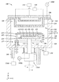
[0017]図1は、処理チャンバ内に配置される基板支持システム102の1つの実施形態を有する処理チャンバ100の側断面図である。処理チャンバ100は、処理容積108を囲む側壁104、底部105、及びリッドアセンブリ106からなるチャンバ本体104を含む。基板支持システム102は、処理容積108内に少なくとも部分的に配置され、且つチャンバ本体104内に形成されたポート112を通して、処理容積108に移送された基板110を支持する。
[0017] FIG. 1 is a cross-sectional side view of a
[0018]基板支持システム102は、ペデスタル114などの第1の基板支持体113、及び端部支持部材116などの第2の基板支持体115を含む。第2の基板支持体115は、第1の基板支持体113の上で基板110を断続的に支持するために使用されてもよい。例えば、図1では、基板110は、ペデスタル114から離れた隙間の中の端部支持部材116上で示される。基板110は、処理中にペデスタル114に近接又は接触するようになる。例えば、ペデスタル114は、処理中に基板110の主要面に接触(又は近接)するように適合される支持面118を含む。したがって、ペデスタル114は、処理チャンバ100内の基板110のための第1の支持構造の役割を果たす。
The
[0019]ペデスタル114及び端部支持部材116のうちの少なくとも1つが、他方に対して可動である。処理位置において、端部支持部材116は、ペデスタル114に近接し、基板110の下面がペデスタル114によって支持されるようにペデスタル114を取り囲んでもよい(すなわち、囲んでもよい)。1つの実施形態では、ペデスタル114は、端部支持部材116に対する運動が可能であってもよい。一例では、端部支持部材116は、少なくともX−Y(水平)平面で、並びに回転式に固定されてもよく、ペデスタル114は、(Z方向の)垂直運動、(軸Aの周りの)回転運動のうちの1つ又はそれらの組み合わせをもたらし、且つさらに(軸Aに対する)角度運動をもたらし得るシャフト121を介して、アクチュエータ126Aに連結される。アクチュエータ126Aによって垂直運動がもたらされてもよく、それにより、基板110が端部支持部材116から支持面118に移送されることが可能になる。別の実施形態では、端部支持部材116は、端部支持部材116の垂直運動(Z方向)を少なくとももたらす1つ又は複数の支持部材(以下でより詳細に説明される)を介して、アクチュエータ126Bに連結されてもよい。したがって、端部支持部材116は、ペデスタル114に対して動かしてもよい。アクチュエータ126Bによって垂直運動がもたらされてもよく、それにより、端部支持部材116が下降し、基板110を支持面118に移送することが可能になる。別の実施形態では、アクチュエータ126A及び126Bによってもたらされる運動の組み合わせが、支持面118と端部支持部材116との間で基板110の移送を促進するために提供されてもよい。
[0019] At least one of the
[0020]処理チャンバ100は、数ある中でも、堆積チャンバ、エッチングチャンバ、イオン注入チャンバ、プラズマ処理チャンバ、又は熱処理チャンバであってもよい。図示の実施形態では、処理チャンバは堆積チャンバであり、シャワーヘッドアセンブリ128を含む。処理容積108は、その中の圧力を制御するために真空システム130と選択的に流体連通してもよい。シャワーヘッドアセンブリ128は、処理ガス源132に連結されてもよく、材料を基板110上に堆積するために処理ガスを処理容積108に供給する。シャワーヘッドアセンブリ128は、シャワーヘッドアセンブリ128の温度を制御する温度制御要素134をさらに含んでもよい。温度制御要素134は、冷却源136と流体連通している流体チャネルであってもよい。
[0020] The
[0021]端部支持部材116は、一時的な基板支持部材として機能する。端部支持部材116は、必要に応じて、(図1で示されるように)ペデスタル114の支持面118から離間された関係で基板110を支持するために利用され、それにより、所望するときにペデスタル114の支持面118に対して基板110を再度位置決めすることを容易にすることができる。端部支持部材116は、中に形成される凹部又はスロット133を含んでもよい。凹部又はスロットは、ロボットブレード109を受け入れるように寸法形成され、それにより、処理容積108内外へのロボット基板移送が容易となる。
[0021] The
[0022]ペデスタル114は、ペデスタル本体122の中に配置される少なくとも1つの組み込み型温度制御要素120を含んでもよい。1つの実施形態では、組み込み型温度制御要素120は、基板110によって吸収される熱エネルギーをペデスタル本体122に適用するために利用される、加熱又は冷却のための要素又はチャネルであってもよい。1つ又は複数の電極及び/又は真空ポートなどの他の要素が、ペデスタル本体122の上に配置されてもよく、又はその中に組み込まれてもよい。基板110の温度は、1つ又は複数のセンサ124によってモニターされてもよい。ペデスタル本体122の種々の領域の温度が個別に加熱又は冷却され得るように、組み込み型温度制御要素120はゾーン制御されてもよい。しかしながら、ペデスタル114内の欠点及び/又は基板110内の不均一などの酌量すべき要因によって、組み込み型温度制御要素120は、支持面118及び/又は基板110全体にわたって熱エネルギーを均一に適用できない場合がある。こうした酌量すべき要因によって、基板110の温度が不均一となり、結果として基板の処理が不均一となる。
[0022] The
[0023]基板110の表面上に存在し得る(基板110の温度をモニターすることによって判定することができる)熱の不均一に対処するため、基板110を支持面118に対して再度位置決めしてもよい。基板110の表面上に存在する熱点又は冷点は、ペデスタル本体122の支持面118の中又はその上の熱点又は冷点を示す。一例では、アクチュエータ126A及び126Bによってもたらされる運動のうちの1つ又は組み合わせによって、基板が支持面118から端部支持部材116に移送される。端部支持部材116は、図示のように、ペデスタル114の上で離間された関係で基板110を一時的に支持し、それにより、基板110に対するペデスタル114の回転が可能となる。この運度は、ペデスタル本体122の支持面118の中又はその上に存在する熱点又は冷点(基板110の温度をモニターすることによって判定される)を再配置するために利用されてもよい。ペデスタル114は、約360度未満、例えば、約1度から約180℃未満の間などの約180度未満の角変位で、又はその間の増分の角変位で回転してもよい。ペデスタル114を回転させることによって、ペデスタル本体122の支持面118の中又はその上に存在する熱点又は冷点を再配置した後、アクチュエータ126A及び126Bによってもたらされる運動のうちの1つ又は組み合わせによって、基板110をペデスタル114の支持面118上に再配置してもよい。基板110の再配置が一旦完了すると、基板110上の冷点をペデスタル114の支持面118上の熱点により近いところに位置決めしてもよく、その反対の操作も可能である。したがって、基板110の表面上の任意の局所化された不均一な温度分布が平均化され、基板全体にわたってほぼ均一な温度分布(すなわち、+/−摂氏数度)がもたらされる。
[0023] The
[0024]別の実施形態では、ペデスタル114は静電チャックであってもよく、ペデスタル114は1つ又は複数の電極121を含んでもよい。例えば、ペデスタル114は、電力を1つ又は複数の電極121に供給する電圧源であり得る電力要素140に連結されてもよい。電圧源は、高周波(RF)コントローラ又は直流(DC)コントローラであってもよい。別の例では、ペデスタル114は、導電性材料から作られ、シャワーヘッドアセンブリ128によって分配される電力要素140BからのRF電力のためのグラウンド経路として機能してもよい。したがって、処理チャンバ100は、RFプラズマ又はDCプラズマを利用して堆積又はエッチング処理を実行してもよい。これらの種類のプラズマは、完全に同心状又は対称状ではない場合があるため、RF又はDCの熱点(すなわち、電磁熱点(electromagnetic hot spots))が基板110上に存在し得る。これらの電磁熱点によって、基板110の表面上に不均一な堆積又は不均一なエッチング速度が生じ得る。
[0024] In another embodiment, the
[0025]基板110の表面上に存在し得る(プラズマシースを観察することによって判定することができる)電磁熱点に対処するため、上述のプロセスに従って、端部支持部材116を使用して基板110を支持面118に対して再度位置決めしてもよい。例えば、不均一なプラズマシースは、プラズマ内の不均一なエネルギー分布を示し得る。任意の電磁熱点を再分布するために基板110を再度位置決めすることが利用され、基板110の表面上の任意の局所化された不均一なエネルギー分布が平均化され、それにより基板全体にわたって平衡したエネルギー分布がもたらされる。
[0025] To address electromagnetic hot spots (which can be determined by observing the plasma sheath) that may be present on the surface of the
[0026]堆積プロセス又はエッチングプロセスにおける処理の間、ペデスタル114は通常回転する。しかしながら、基板110の位置が支持面118に対して固定されるとき、基板110上に存在すると判定された温度分布、電気バイアス、又は電磁エネルギー分布における任意の異常が固定化する。しかしながら、支持面118に対する基板110の運動は、これらの違いを平均化することによって、温度、電気バイアス、電磁エネルギー分布におけるこれらの違いを補い、結果として基板110上でほぼ均一な温度分布、電気バイアス、又は電磁エネルギー分布が生じる。
[0026] During processing in the deposition or etching process, the
[0027]1つの実施形態では、ペデスタル114に加えて、基板支持システム102は、1つ又は複数のピン142によって支持されている端部支持部材116を含む。1つ又は複数のピン142のうちの少なくとも1つは、リニアドライバ144に直接連結されてもよく、又は図示されているようにリフトリング146に連結されてもよい。さらに、端部支持部材116は、基板110の支持に使用されていないときは遮蔽機能をもたらす堆積リングであってもよい。例えば、基板110がペデスタル114の支持面118によって支持され、端部支持部材116がペデスタル114を少なくとも部分的に囲んでいるとき、端部支持部材116は、チャンバ構成要素を堆積又はエッチングの副生成物から遮蔽してもよい。1つの実施形態では、基板110を処理する間、端部支持部材116は、基板110と部分的に接触したままであってもよい。1つの態様では、端部支持部材116は、処理の間(処理の間にペデスタル114が回転しないとき)に基板110の外周を支持するために利用されてもよい。別の態様では、端部支持部材116は、例えば、メッキ処理において基板110に電気バイアスをもたらすために使用され得る導電性材料から作られてもよい。端部支持部材116は、ペデスタル114に対する端部支持部材の運動を提供するアクチュエータ126Bに連結されているように示されているが、端部支持部材116は、ピン142の上面に単純に置かれてもよい。この実施形態では、ペデスタル114は、端部支持部材116に対して動いてもよく、それにより、基板110が支持面118に移送されることが可能となる。Z方向のペデスタル114の継続運動によって、次いで、端部支持部材116が、ペデスタル114内に形成される周辺ショルダー領域147によって支持されることが可能となる。端部支持部材116がピン142の高さを越えて上昇するにつれて、ペデスタル114、基板110、及び端部支持部材116の回転運動が可能となる。
[0027] In one embodiment, in addition to the
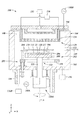
[0028]図2は、処理チャンバ内に配置される基板支持システム202の別の実施形態を有する処理チャンバ100の側断面図である。図1に記載された実施形態のように、基板支持システム202は、ペデスタル114及びアクチュエータ126A、並びに関連するリフト部材及び密封部材を含む。しかしながら、この実施形態では、基板支持システム202の第2の基板支持体203は、図1に示される端部支持部材116の代わりに複数の端部支持部材204を含む。端部支持部材204は、使用時に基板110の端部を選択的に支持する個別のフィンガであってもよい。この実施形態では、ペデスタル114は、それぞれの端部支持部材204に対応する切り抜き領域206を含む。各切り抜き領域206によって、それぞれの端部支持部材204がペデスタル114の底面208を一掃することが可能になり、それにより、基板110がペデスタルの支持面118上で支持されているとき、ペデスタル114が自由回転することが可能になる。端部支持部材204の昇降は、アクチュエータ126B、リフトリング146、及び関連するピン142によって達成されてもよい。
[0028] FIG. 2 is a cross-sectional side view of a
[0029]図3は、図2のペデスタル114の平面図である。3つの端部支持部材204がそれぞれの切り抜き領域206内に示される。ペデスタル114及び/又はアクチュエータ216A(図2に示される)に連結されているエンコーダ又は他の回転検知/インデックス作成計量計を使用することによって、ペデスタル114の支持面118から基板110が離間されるように端部支持部材204が利用されているときにペデスタル114のそれぞれの切り抜き領域206をそれぞれの端部支持部材204と位置合わせしてもよい。3つの端部支持部材204のみが示されているが、第2の基板支持体203は、少なくとも2つの端部支持部材204及び4つ以上の端部支持部材204を含んでもよい。端部支持部材204の数は、切り抜き領域206の対応する数と一致してもよい。任意選択的に又は追加的に、追加の切り抜き領域206(点線で示されている)がペデスタル114に追加されてもよい。切り抜き領域206は、端部支持部材204との位置合わせを容易にしつつ、120度単位で、60度単位で、30度単位で、並びに30度未満の単位でペデスタル114の回転を提供するために必要に応じて利用されてもよい。120度よりも大きい単位で端部支持部材204との位置合わせを容易にするため、追加の切り抜き領域206がさらに追加されてもよい。
[0029] FIG. 3 is a plan view of the
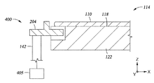
[0030]図4は、第2の基板支持体400の別の実施形態を示すペデスタル114の一部の断面図である。この実施形態では、端部支持部材204は、アクチュエータ405に連結されているピン142に連結されている。他の実施形態と同じように、アクチュエータ405は、ペデスタル114に対して基板110をZ方向に昇降させるために利用される。しかしながら、この実施形態では、アクチュエータ405は、ペデスタル114に対して端部支持部材204を横方向に(X方向に)に動かすために利用される。図示されていないが、他のピン142及び端部支持部材204は、図2に記載された実施形態と同じように、ペデスタル114の外周周辺に配置されてもよい。この実施形態では、アクチュエータ405は、各端部支持部材204につき必要である場合がある。
[0030] FIG. 4 is a cross-sectional view of a portion of
[0031]図5は、基板製造プロセスの間に基板処理特性の不均一を補正する方法500を示すフロー図である。方法500は、本明細書に記載されている基板支持システム102又は202、或いはその他の適切な装置を利用して実行されてもよい。方法500は、ブロック505では、基板110を処理チャンバ100内のペデスタル114に移送することを含む。ブロック505における方法は、ロボットブレード109上で基板110を処理チャンバ100内に移送することと、ロボットブレード109から基板を第2の基板支持体に移送することとをさらに含んでもよい。図1の実施形態では、ブロック505に含まれる移送は、移送ポート112を通って延在するロボットブレード109を受け入れるように構成される平面上において端部支持部材116、特にスロット133を位置合わせすることをさらに含む。一旦基板110が端部支持部材116とほぼ同心状となれば、移送ポート112を通してロボットブレード109を処理チャンバ100から後退させてもよい。端部支持部材204が利用される図2又は図4の実施形態では、ブロック505で説明された移送は、基板110を、ペデスタル114の上に、ペデスタル114とほぼ同心状に、及び端部支持部材204の外周によって画定されている領域の上に位置決めすることを含む。アクチュエータ126B(図2に示される)又はアクチュエータ405(図4に示される)は、次いで、端部支持部材204を基板110の端部付近に動かすために使用されてもよい。この実施形態では、端部支持部材204は、ロボットブレード109の走行路を妨げないように離間されてもよい。一旦端部支持部材204が基板110の端部を掴むと、基板110はロボットブレード109から持ち上げられてもよく、ロボットブレード109は後退してもよい。
[0031] FIG. 5 is a flow diagram illustrating a
[0032]ブロック510では、図1の端部支持部材116或いは図2及び図4の端部支持部材204のいずれかを使用して、基板110がペデスタル114の支持面118に下降する。基板110は、ペデスタル114の支持面118上の第1の位置に位置決めされてもよい。図1の実施形態では、端部支持部材116は、ペデスタル114の支持面118が少なくとも部分的に基板110を支持するまで下降してもよく、且つ周辺ショルダー領域147に近接するようにさらに下降してもよい。図2の実施形態では、端部支持部材204は、ペデスタル114の支持面118が少なくとも部分的に基板110を支持するまで下降してもよく、且つペデスタル114の底面208を一掃するためにさらに下降してもよい。図4の実施形態では、端部支持部材204は、ペデスタル114の側壁を一掃するためにX方向に作動してもよい。これらのいずれの実施形態でも、基板110の主要面(例えば、底部又は裏面)は、ペデスタル114の支持面118によって支持され、基板110は処理されてもよい。
[0032] In
[0033]ブロック515では、基板110の主要面がペデスタル114によって支持されている際に基板110を処理するため、ペデスタル114及びその上に支持されている基板110は、回転、上昇、下降してもよく、並びにこれらの動作の組み合わせが行われてもよい。例えば、基板110がペデスタル114上で支持されている際に処理チャンバ100内で生成され得るそのガス又はプラズマを使用する堆積又はエッチング処理である。基板110の処理は、シャワーヘッドアセンブリ128に対してペデスタル114を上昇又は下降させることを含んでもよい。基板110の処理には、ペデスタル114の回転も含まれてもよい。
[0033] In
[0034]ブロック520では、基板110上で実行される処理がモニターされる。所望のパラメータ又は目標値の範囲外にあると判断される基板の任意の不均一を判定するため、基板の温度、電気バイアス、及び/又は電磁エネルギー分布(すなわち、基板処理特性)などの測定基準を基板110の表面にわたってモニターしてもよい。所望のパラメータ又は目標値には、処理パラメータの狭い範囲(すなわち、ウィンドウ)内にある基板温度、電気バイアス、及び/又は基板110上の電磁エネルギー分布が含まれてもよい。温度に関しては、所望のパラメータ又は目標値は、摂氏数度内で変動する温度を含んでもよい。測定基準が、均一条件(すなわち、所望のパラメータ又は目標値の範囲内)を示す場合、基板110の処理を継続してもよい。不均一(すなわち、所望のパラメータ又は目標値の範囲外の測定基準)が存在する場合、この方法は、基板110をペデスタル114の支持面118上で再度位置決めすることを含むブロック525に進む。
[0034] At
[0035]ブロック520で説明されたインシトゥ処理(in−situ process)は、任意であってもよい。処理基板のモニタリングは、不均一の存在を判定するために方法500で用いられてもよい。このエクスシトゥモニタリング(ex−situ monitoring)は、特定の方策を使用して後続の基板を処理するための位置決めパラメータを決定するために利用されてもよい。例えば、エクスシトゥモニタリングは、ペデスタル114の回転の角度、ペデスタル114上の基板110の再度位置決めの量(すなわち、回数)、ペデスタル114上の基板110の再度位置決めのタイミング、及びそれらの組み合わせを決定するために利用されてもよい。したがって、ブロック520で説明されたインシトゥ処理及び/又はエクスシトゥモニタリングのいずれかによって、一旦不均一が判定されたら、特定の製造スキームに対してモニタリングが延期されてもよい。
[0035] The in-situ process described in
[0036]ブロック525では、図1の実施形態において、基板110がペデスタル114の支持面118から離間されているとき、図1の端部支持部材116が基板110を支持するために使用される。この離間された関係では、ペデスタル114は、約360度未満の幾らかの単位で回転してもよい。図2及び図4の実施形態では、端部支持部材204は、基板110を支持し、且つ基板110をペデスタル114の支持面118から離すように使用され、それにより、ペデスタル114が約360度未満の幾らかの単位で回転することが可能となる。ブロック510で説明されたように、ペデスタル114が回転した後、基板110は、ペデスタル114の支持面118上に再度位置決めされてもよい。ブロック515で説明された処理が継続してもよい。処理の間、ブロック515に続いて、ブロック520及びブロック525で説明されたように処理がモニターされてもよく、処理が完了するまで必要に応じて繰り返されてもよい。処理が完了したとき、ブロック525で説明されたように、基板110をペデスタル114の支持面118から離間させることによって、次いで基板110を処理チャンバ100の外に移送してもよく、基板110を端部支持部材116(図1)又は端部支持部材204(図2及び図4)からロボットブレード109に移送する処理が実行されてもよい。基板110をロボットブレード109に移送することは、ブロック505で説明された処理と実質的に逆の手順であってもよい。
[0036] At
[0037]基板支持システム102又は202の実施形態は、基板処理特性の中の不均一を補うインシトゥ(チャンバ内)処理を可能にする。本明細書に記載された本発明の基板支持システム102又は202は、処理チャンバから基板を取り除くことなく、及び/又は、ロボットブレード(又はその他の周辺基板支持機構)を使用して基板を一時的に支持するために真空を破壊することなく、基板処理特性を補正することができるため、コストを削減し、スループットを増大させることができる。さらに、基板処理特性の不均一を最小限に抑えたり、取り除いたりして、基板のすべての部分に均一な堆積をもたらすため、装置の品質及び/又は装置の収率を強化することができる。
[0037] Embodiments of the
[0038]以上の説明は本開示の実施形態を対象としているが、本開示の基本的な範囲を逸脱することなく、本開示の他の実施形態及び追加の実施形態を考案してもよく、本開示の範囲は、添付の特許請求の範囲によって定められる。 [0038] While the above description is directed to embodiments of the present disclosure, other and additional embodiments of the present disclosure may be devised without departing from the basic scope of the disclosure, The scope of the present disclosure is defined by the appended claims.
Claims (16)
処理領域を囲むチャンバ本体、
前記処理領域内に少なくとも部分的に配置される第1の基板支持体及び第2の基板支持体を備え、前記第2の基板支持体は前記第1の基板支持体を取り囲み、前記第1の基板支持体及び前記第2の基板支持体のうちの片方又は両方は互いに対して直線的に可動であり、且つ前記第1の基板支持体は前記第2の基板支持体に対して回転可能である、基板処理チャンバ。 A substrate processing chamber,
A chamber body surrounding the processing area,
A first substrate support and a second substrate support disposed at least partially within the processing region, wherein the second substrate support surrounds the first substrate support; One or both of the substrate support and the second substrate support are linearly movable relative to each other, and the first substrate support is rotatable with respect to the second substrate support. A substrate processing chamber.
ペデスタル、及び
前記ペデスタルを回転するように動作可能なアクチュエータを備える、請求項1に記載の処理チャンバ。 The first substrate support comprises:
The processing chamber of claim 1, comprising a pedestal and an actuator operable to rotate the pedestal.
基板の端部を支持するための単一の端部支持部材を備える、請求項2に記載の処理チャンバ。 The second substrate support is
The processing chamber of claim 2, comprising a single end support member for supporting an end of the substrate.
基板の端部を支持するための複数の端部支持部材を備える、請求項2に記載の処理チャンバ。 The second substrate support is
The processing chamber of claim 2, comprising a plurality of end support members for supporting the end of the substrate.
処理領域を囲むチャンバ本体、
基板の主要面を支持するために前記処理領域内に配置されるペデスタル、及び
前記基板の前記主要面が前記ペデスタルによって支持されていないときに前記基板の端部を断続的に支持するために前記処理領域内に配置される端部支持部材を備え、前記ペデスタルが前記端部支持部材に対して回転可能である、基板処理チャンバ。 A substrate processing chamber,
A chamber body surrounding the processing area,
A pedestal disposed in the processing region to support a major surface of the substrate, and the pedestal to intermittently support an edge of the substrate when the major surface of the substrate is not supported by the pedestal. A substrate processing chamber comprising an end support member disposed in a processing region, wherein the pedestal is rotatable relative to the end support member.
複数の端部支持部材、及び
前記複数の端部支持部材を垂直方向に動かすように動作可能なアクチュエータを備える、請求項11に記載の処理チャンバ。 The end support member is
The processing chamber of claim 11, comprising a plurality of end support members and an actuator operable to move the plurality of end support members in a vertical direction.
Applications Claiming Priority (3)
| Application Number | Priority Date | Filing Date | Title |
|---|---|---|---|
| US201361872545P | 2013-08-30 | 2013-08-30 | |
| US61/872,545 | 2013-08-30 | ||
| PCT/US2014/050227 WO2015031023A1 (en) | 2013-08-30 | 2014-08-07 | Substrate support system |
Publications (2)
| Publication Number | Publication Date |
|---|---|
| JP2016529733A true JP2016529733A (en) | 2016-09-23 |
| JP2016529733A5 JP2016529733A5 (en) | 2017-09-14 |
Family
ID=52583785
Family Applications (1)
| Application Number | Title | Priority Date | Filing Date |
|---|---|---|---|
| JP2016538940A Pending JP2016529733A (en) | 2013-08-30 | 2014-08-07 | Substrate support system |
Country Status (6)
| Country | Link |
|---|---|
| US (1) | US20150064809A1 (en) |
| JP (1) | JP2016529733A (en) |
| KR (1) | KR20160047540A (en) |
| CN (1) | CN105493262B (en) |
| TW (1) | TWI673821B (en) |
| WO (1) | WO2015031023A1 (en) |
Families Citing this family (21)
| Publication number | Priority date | Publication date | Assignee | Title |
|---|---|---|---|---|
| US9966240B2 (en) | 2014-10-14 | 2018-05-08 | Applied Materials, Inc. | Systems and methods for internal surface conditioning assessment in plasma processing equipment |
| US9355922B2 (en) | 2014-10-14 | 2016-05-31 | Applied Materials, Inc. | Systems and methods for internal surface conditioning in plasma processing equipment |
| US9691645B2 (en) | 2015-08-06 | 2017-06-27 | Applied Materials, Inc. | Bolted wafer chuck thermal management systems and methods for wafer processing systems |
| US9741593B2 (en) | 2015-08-06 | 2017-08-22 | Applied Materials, Inc. | Thermal management systems and methods for wafer processing systems |
| US10504700B2 (en) | 2015-08-27 | 2019-12-10 | Applied Materials, Inc. | Plasma etching systems and methods with secondary plasma injection |
| KR102104468B1 (en) * | 2015-12-30 | 2020-04-27 | 맷슨 테크놀로지, 인크. | Methods for improving process uniformity in millisecond annealing systems |
| KR20180099776A (en) | 2016-01-26 | 2018-09-05 | 어플라이드 머티어리얼스, 인코포레이티드 | Wafer edge ring lifting solution |
| US9947517B1 (en) | 2016-12-16 | 2018-04-17 | Applied Materials, Inc. | Adjustable extended electrode for edge uniformity control |
| US10553404B2 (en) | 2017-02-01 | 2020-02-04 | Applied Materials, Inc. | Adjustable extended electrode for edge uniformity control |
| US10571069B2 (en) * | 2017-09-14 | 2020-02-25 | Applied Materials, Inc. | Gimbal assembly for heater pedestal |
| US11075105B2 (en) | 2017-09-21 | 2021-07-27 | Applied Materials, Inc. | In-situ apparatus for semiconductor process module |
| US11043400B2 (en) | 2017-12-21 | 2021-06-22 | Applied Materials, Inc. | Movable and removable process kit |
| JP6971865B2 (en) * | 2018-01-17 | 2021-11-24 | キオクシア株式会社 | Processing equipment |
| JP6770988B2 (en) * | 2018-03-14 | 2020-10-21 | 株式会社Kokusai Electric | Manufacturing method for substrate processing equipment and semiconductor equipment |
| US10790123B2 (en) | 2018-05-28 | 2020-09-29 | Applied Materials, Inc. | Process kit with adjustable tuning ring for edge uniformity control |
| US11935773B2 (en) | 2018-06-14 | 2024-03-19 | Applied Materials, Inc. | Calibration jig and calibration method |
| US11289310B2 (en) | 2018-11-21 | 2022-03-29 | Applied Materials, Inc. | Circuits for edge ring control in shaped DC pulsed plasma process device |
| US11101115B2 (en) | 2019-04-19 | 2021-08-24 | Applied Materials, Inc. | Ring removal from processing chamber |
| CN112542370B (en) * | 2019-09-23 | 2024-04-05 | 中微半导体设备(上海)股份有限公司 | Plasma processor and heater assembly thereof |
| US20220157572A1 (en) * | 2020-11-18 | 2022-05-19 | Applied Materials, Inc. | Deposition ring for thin substrate handling via edge clamping |
| KR20230164168A (en) * | 2021-04-02 | 2023-12-01 | 어플라이드 머티어리얼스, 인코포레이티드 | Process cell for baking process after field guided exposure |
Citations (6)
| Publication number | Priority date | Publication date | Assignee | Title |
|---|---|---|---|---|
| JP2000286328A (en) * | 1999-03-31 | 2000-10-13 | Tokyo Electron Ltd | Gas treatment apparatus |
| JP2002050809A (en) * | 2000-08-01 | 2002-02-15 | Anelva Corp | Substrate treating device and method |
| JP2002174502A (en) * | 2000-12-07 | 2002-06-21 | Ulvac Japan Ltd | Axial aligner, film thickness measuring apparatus, film forming apparatus, method and apparatus for measuring film thickness |
| JP2003115527A (en) * | 2001-10-05 | 2003-04-18 | Sumitomo Heavy Ind Ltd | Substrate transfer system |
| JP2009135228A (en) * | 2007-11-29 | 2009-06-18 | Nuflare Technology Inc | Vapor phase growth apparatus and vapor phase growth method |
| JP2011181873A (en) * | 2010-03-04 | 2011-09-15 | Nissin Ion Equipment Co Ltd | Wafer lift rotating mechanism, stage device and ion implantation device |
Family Cites Families (15)
| Publication number | Priority date | Publication date | Assignee | Title |
|---|---|---|---|---|
| US5982986A (en) * | 1995-02-03 | 1999-11-09 | Applied Materials, Inc. | Apparatus and method for rotationally aligning and degassing semiconductor substrate within single vacuum chamber |
| US6217663B1 (en) * | 1996-06-21 | 2001-04-17 | Kokusai Electric Co., Ltd. | Substrate processing apparatus and substrate processing method |
| US6068441A (en) * | 1997-11-21 | 2000-05-30 | Asm America, Inc. | Substrate transfer system for semiconductor processing equipment |
| US6776849B2 (en) * | 2002-03-15 | 2004-08-17 | Asm America, Inc. | Wafer holder with peripheral lift ring |
| US7128806B2 (en) * | 2003-10-21 | 2006-10-31 | Applied Materials, Inc. | Mask etch processing apparatus |
| US7198677B2 (en) * | 2005-03-09 | 2007-04-03 | Wafermasters, Inc. | Low temperature wafer backside cleaning |
| ITTO20060131A1 (en) * | 2006-02-24 | 2007-08-25 | Fiat Auto Spa | CONTROL DEVICE FOR THE HANDLING OF A VALVE IN PARTICULAR OF AN INTERNAL COMBUSTION ENGINE SUCTION VALVE |
| JP2007242858A (en) * | 2006-03-08 | 2007-09-20 | Wafermasters Inc | Wafer processing system and method of processing |
| JP4949091B2 (en) * | 2007-03-16 | 2012-06-06 | 東京エレクトロン株式会社 | Substrate processing apparatus, substrate processing method, and recording medium |
| US20100248397A1 (en) * | 2009-03-26 | 2010-09-30 | Tokyo Electron Limited | High temperature susceptor having improved processing uniformity |
| JP5341706B2 (en) * | 2009-10-16 | 2013-11-13 | 株式会社ニューフレアテクノロジー | Semiconductor manufacturing apparatus and semiconductor manufacturing method |
| JP5527166B2 (en) * | 2010-11-05 | 2014-06-18 | 住友電気工業株式会社 | Heating apparatus and vapor phase growth apparatus |
| WO2012134663A2 (en) * | 2011-03-16 | 2012-10-04 | Applied Materials, Inc | Method and apparatus utilizing a single lift mechanism for processing and transfer of substrates |
| US9870919B2 (en) * | 2012-04-25 | 2018-01-16 | Applied Materials, Inc. | Process chamber having separate process gas and purge gas regions |
| KR102449103B1 (en) * | 2014-03-12 | 2022-09-28 | 어플라이드 머티어리얼스, 인코포레이티드 | Wafer rotation in a semiconductor chamber |
-
2014
- 2014-08-07 CN CN201480047900.XA patent/CN105493262B/en not_active Expired - Fee Related
- 2014-08-07 WO PCT/US2014/050227 patent/WO2015031023A1/en active Application Filing
- 2014-08-07 KR KR1020167007843A patent/KR20160047540A/en not_active Application Discontinuation
- 2014-08-07 JP JP2016538940A patent/JP2016529733A/en active Pending
- 2014-08-08 US US14/455,028 patent/US20150064809A1/en not_active Abandoned
- 2014-08-29 TW TW103129966A patent/TWI673821B/en not_active IP Right Cessation
Patent Citations (6)
| Publication number | Priority date | Publication date | Assignee | Title |
|---|---|---|---|---|
| JP2000286328A (en) * | 1999-03-31 | 2000-10-13 | Tokyo Electron Ltd | Gas treatment apparatus |
| JP2002050809A (en) * | 2000-08-01 | 2002-02-15 | Anelva Corp | Substrate treating device and method |
| JP2002174502A (en) * | 2000-12-07 | 2002-06-21 | Ulvac Japan Ltd | Axial aligner, film thickness measuring apparatus, film forming apparatus, method and apparatus for measuring film thickness |
| JP2003115527A (en) * | 2001-10-05 | 2003-04-18 | Sumitomo Heavy Ind Ltd | Substrate transfer system |
| JP2009135228A (en) * | 2007-11-29 | 2009-06-18 | Nuflare Technology Inc | Vapor phase growth apparatus and vapor phase growth method |
| JP2011181873A (en) * | 2010-03-04 | 2011-09-15 | Nissin Ion Equipment Co Ltd | Wafer lift rotating mechanism, stage device and ion implantation device |
Also Published As
| Publication number | Publication date |
|---|---|
| CN105493262B (en) | 2019-02-15 |
| WO2015031023A1 (en) | 2015-03-05 |
| TWI673821B (en) | 2019-10-01 |
| US20150064809A1 (en) | 2015-03-05 |
| TW201523785A (en) | 2015-06-16 |
| KR20160047540A (en) | 2016-05-02 |
| CN105493262A (en) | 2016-04-13 |
Similar Documents
| Publication | Publication Date | Title |
|---|---|---|
| JP2016529733A (en) | Substrate support system | |
| JP3209624U (en) | Control of RF amplitude of edge ring of capacitively coupled plasma processing equipment | |
| US10541168B2 (en) | Edge ring centering method using ring dynamic alignment data | |
| JP6976686B2 (en) | Systems and methods for performing edge ring characterization | |
| CN108369922B (en) | Wafer edge ring lifting solution | |
| KR102413035B1 (en) | Pixelated temperature controlled substrate support assembly | |
| CN105810609B (en) | Movable edge coupling ring for controlling edge processing during semiconductor wafer processing | |
| JP5992334B2 (en) | Shadow ring to correct wafer edge and bevel deposition | |
| KR102627019B1 (en) | Pin lifter assembly with small gap | |
| US20180053629A1 (en) | Control of on-wafer cd uniformity with movable edge ring and gas injection adjustment | |
| CN110062954B (en) | Processing assembly design for in-chamber heater and wafer rotation mechanism | |
| TWI735509B (en) | Plasma processing device and control method | |
| JP2020512701A (en) | Bottom and middle edge rings | |
| JP2023156415A (en) | Movable edge ring design | |
| KR20200089616A (en) | Plasma processing apparatus and method for measuring misalignment of ring member | |
| CN110993477A (en) | Plasma processing apparatus and method for measuring thickness of ring member | |
| CN110574149B (en) | Gimbal Assembly for Heater Base | |
| CN116917533A (en) | Substrate support, method of processing substrate, and processing system | |
| TW201918120A (en) | Focus ring, plasma apparatus comprising the focus ring and method for adjusting voltage use the focus ring |
Legal Events
| Date | Code | Title | Description |
|---|---|---|---|
| A521 | Request for written amendment filed |
Free format text: JAPANESE INTERMEDIATE CODE: A523 Effective date: 20170807 |
|
| A621 | Written request for application examination |
Free format text: JAPANESE INTERMEDIATE CODE: A621 Effective date: 20170807 |
|
| A977 | Report on retrieval |
Free format text: JAPANESE INTERMEDIATE CODE: A971007 Effective date: 20180530 |
|
| A131 | Notification of reasons for refusal |
Free format text: JAPANESE INTERMEDIATE CODE: A131 Effective date: 20180605 |
|
| A521 | Request for written amendment filed |
Free format text: JAPANESE INTERMEDIATE CODE: A523 Effective date: 20180904 |
|
| A131 | Notification of reasons for refusal |
Free format text: JAPANESE INTERMEDIATE CODE: A131 Effective date: 20180925 |
|
| A02 | Decision of refusal |
Free format text: JAPANESE INTERMEDIATE CODE: A02 Effective date: 20190521 |