US6451663B1 - Method of manufacturing a cylindrical storage node in a semiconductor device - Google Patents
Method of manufacturing a cylindrical storage node in a semiconductor device Download PDFInfo
- Publication number
- US6451663B1 US6451663B1 US09/983,348 US98334801A US6451663B1 US 6451663 B1 US6451663 B1 US 6451663B1 US 98334801 A US98334801 A US 98334801A US 6451663 B1 US6451663 B1 US 6451663B1
- Authority
- US
- United States
- Prior art keywords
- storage node
- conductive layer
- semiconductor device
- hole
- manufacturing
- Prior art date
- Legal status (The legal status is an assumption and is not a legal conclusion. Google has not performed a legal analysis and makes no representation as to the accuracy of the status listed.)
- Expired - Fee Related
Links
- 238000003860 storage Methods 0.000 title claims abstract description 50
- 239000004065 semiconductor Substances 0.000 title claims abstract description 35
- 238000004519 manufacturing process Methods 0.000 title claims abstract description 25
- 238000000034 method Methods 0.000 claims abstract description 54
- 239000000463 material Substances 0.000 claims description 36
- 238000000465 moulding Methods 0.000 claims description 23
- 239000012212 insulator Substances 0.000 claims description 21
- 238000005530 etching Methods 0.000 claims description 12
- 239000007789 gas Substances 0.000 claims description 12
- 229920002120 photoresistant polymer Polymers 0.000 claims description 8
- IJGRMHOSHXDMSA-UHFFFAOYSA-N Atomic nitrogen Chemical compound N#N IJGRMHOSHXDMSA-UHFFFAOYSA-N 0.000 claims description 6
- 239000005368 silicate glass Substances 0.000 claims description 6
- 238000000151 deposition Methods 0.000 claims description 4
- 229920003209 poly(hydridosilsesquioxane) Polymers 0.000 claims description 4
- XPDWGBQVDMORPB-UHFFFAOYSA-N Fluoroform Chemical group FC(F)F XPDWGBQVDMORPB-UHFFFAOYSA-N 0.000 claims description 3
- BPQQTUXANYXVAA-UHFFFAOYSA-N Orthosilicate Chemical compound [O-][Si]([O-])([O-])[O-] BPQQTUXANYXVAA-UHFFFAOYSA-N 0.000 claims description 3
- 238000004380 ashing Methods 0.000 claims description 3
- QVGXLLKOCUKJST-UHFFFAOYSA-N atomic oxygen Chemical compound [O] QVGXLLKOCUKJST-UHFFFAOYSA-N 0.000 claims description 3
- 239000011521 glass Substances 0.000 claims description 3
- 239000000203 mixture Substances 0.000 claims description 3
- 229910052757 nitrogen Inorganic materials 0.000 claims description 3
- 239000001301 oxygen Substances 0.000 claims description 3
- 229910052760 oxygen Inorganic materials 0.000 claims description 3
- 238000002955 isolation Methods 0.000 abstract description 7
- 239000010410 layer Substances 0.000 description 67
- 229910021420 polycrystalline silicon Inorganic materials 0.000 description 8
- 229920005591 polysilicon Polymers 0.000 description 8
- 150000004767 nitrides Chemical class 0.000 description 6
- KRHYYFGTRYWZRS-UHFFFAOYSA-N Fluorane Chemical compound F KRHYYFGTRYWZRS-UHFFFAOYSA-N 0.000 description 4
- 239000011229 interlayer Substances 0.000 description 4
- 230000007547 defect Effects 0.000 description 3
- 229910000040 hydrogen fluoride Inorganic materials 0.000 description 3
- 239000000758 substrate Substances 0.000 description 3
- 239000003990 capacitor Substances 0.000 description 2
- 230000007423 decrease Effects 0.000 description 2
- 235000019892 Stellar Nutrition 0.000 description 1
- VRZFDJOWKAFVOO-UHFFFAOYSA-N [O-][Si]([O-])([O-])O.[B+3].P Chemical compound [O-][Si]([O-])([O-])O.[B+3].P VRZFDJOWKAFVOO-UHFFFAOYSA-N 0.000 description 1
- 238000013459 approach Methods 0.000 description 1
- 238000005229 chemical vapour deposition Methods 0.000 description 1
- 239000013065 commercial product Substances 0.000 description 1
- 238000007796 conventional method Methods 0.000 description 1
- 230000003628 erosive effect Effects 0.000 description 1
- 230000010354 integration Effects 0.000 description 1
- 238000000206 photolithography Methods 0.000 description 1
- 238000005498 polishing Methods 0.000 description 1
- 238000012552 review Methods 0.000 description 1
- 238000012360 testing method Methods 0.000 description 1
- 238000012876 topography Methods 0.000 description 1
- 238000001039 wet etching Methods 0.000 description 1
Images

Classifications
-
- H—ELECTRICITY
- H10—SEMICONDUCTOR DEVICES; ELECTRIC SOLID-STATE DEVICES NOT OTHERWISE PROVIDED FOR
- H10B—ELECTRONIC MEMORY DEVICES
- H10B12/00—Dynamic random access memory [DRAM] devices
-
- H—ELECTRICITY
- H01—ELECTRIC ELEMENTS
- H01L—SEMICONDUCTOR DEVICES NOT COVERED BY CLASS H10
- H01L28/00—Passive two-terminal components without a potential-jump or surface barrier for integrated circuits; Details thereof; Multistep manufacturing processes therefor
- H01L28/40—Capacitors
- H01L28/60—Electrodes
- H01L28/82—Electrodes with an enlarged surface, e.g. formed by texturisation
- H01L28/90—Electrodes with an enlarged surface, e.g. formed by texturisation having vertical extensions
- H01L28/91—Electrodes with an enlarged surface, e.g. formed by texturisation having vertical extensions made by depositing layers, e.g. by depositing alternating conductive and insulating layers
-
- H—ELECTRICITY
- H01—ELECTRIC ELEMENTS
- H01L—SEMICONDUCTOR DEVICES NOT COVERED BY CLASS H10
- H01L21/00—Processes or apparatus adapted for the manufacture or treatment of semiconductor or solid state devices or of parts thereof
- H01L21/02—Manufacture or treatment of semiconductor devices or of parts thereof
- H01L21/04—Manufacture or treatment of semiconductor devices or of parts thereof the devices having potential barriers, e.g. a PN junction, depletion layer or carrier concentration layer
- H01L21/18—Manufacture or treatment of semiconductor devices or of parts thereof the devices having potential barriers, e.g. a PN junction, depletion layer or carrier concentration layer the devices having semiconductor bodies comprising elements of Group IV of the Periodic Table or AIIIBV compounds with or without impurities, e.g. doping materials
- H01L21/30—Treatment of semiconductor bodies using processes or apparatus not provided for in groups H01L21/20 - H01L21/26
- H01L21/31—Treatment of semiconductor bodies using processes or apparatus not provided for in groups H01L21/20 - H01L21/26 to form insulating layers thereon, e.g. for masking or by using photolithographic techniques; After treatment of these layers; Selection of materials for these layers
- H01L21/3205—Deposition of non-insulating-, e.g. conductive- or resistive-, layers on insulating layers; After-treatment of these layers
- H01L21/321—After treatment
- H01L21/32115—Planarisation
- H01L21/3212—Planarisation by chemical mechanical polishing [CMP]
-
- Y—GENERAL TAGGING OF NEW TECHNOLOGICAL DEVELOPMENTS; GENERAL TAGGING OF CROSS-SECTIONAL TECHNOLOGIES SPANNING OVER SEVERAL SECTIONS OF THE IPC; TECHNICAL SUBJECTS COVERED BY FORMER USPC CROSS-REFERENCE ART COLLECTIONS [XRACs] AND DIGESTS
- Y10—TECHNICAL SUBJECTS COVERED BY FORMER USPC
- Y10S—TECHNICAL SUBJECTS COVERED BY FORMER USPC CROSS-REFERENCE ART COLLECTIONS [XRACs] AND DIGESTS
- Y10S438/00—Semiconductor device manufacturing: process
- Y10S438/942—Masking
- Y10S438/948—Radiation resist
- Y10S438/949—Energy beam treating radiation resist on semiconductor
Definitions
- the present invention refers to a method of manufacturing a cylindrical storage node in a semiconductor device with a minimum loss difference of a conductive layer between the center and the edge of cell areas during an etch-back process of storage node isolation.
- the method of manufacturing a cylindrical storage node according to the present invention maintains electric capacitance uniformity over the entire cell area of a wafer and results in improved device reliability.
- a semiconductor memory device like a dynamic random access memory (DRAM) includes cell capacitors for storing data.
- DRAM dynamic random access memory
- cylindrical stack structures are known as universal capacitor structures.
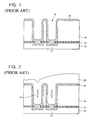
- a poly plug 12 for bit line BC contacts is produced in an interlayer insulator 10 , and a nitride layer is deposited as an etch stopping layer 14 .
- a molding oxide layer 16 is deposited on the nitride layer 14 , and a hole 18 is produced in the molding oxide layer 16 using a photolithographic etch process.
- the nitride layer 14 exposed in the bottom of the hole 18 , is removed in an etch-back process and the poly plug 12 is exposed.
- a storage conductive layer 20 is deposited to a uniform thickness.
- a plugging material 22 is deposited to fill-up the inside of the hole 18 on the storage conductive layer 20 .
- the plugging material 22 protects the bottom of the hole 18 in the storage node from being etched completely in the etch-back process of isolating the storage node.
- the height of the deposited plugging material 22 in the center area of the cell having the holes 18 is lower than the height of the deposited plugging material 22 in the cell surrounding areas without the holes 18 in an amount of 2500 to 3000 ⁇ .
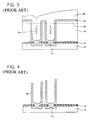
- the time required to complete any etch-back process can be calculated by determining the average etch rate of the process and calculating the time necessary to etch through the layer. Etching is then allowed to continue for an over-etch period necessary to compensate any etch rate non-uniformity, layer thickness non-uniformity, or underlying topography. It is generally desirable to minimize the over-etch time so that the erosion of the underlying layer is minimized. A method of determining the nominal etching endpoint of the process allows such a reduction in over-etch time.
- the endpoint of the etch-back process as illustrated in FIG. 3 is an etching time required for completely removing the storage conductive layer in cell surrounding areas.
- the etch-back process removes the plugging material 22 and the storage conductive layer 20 up to the location indicated by a broken line 30 in FIG. 3 .
- Isolation for the storage node is then achieved among each of the holes 18 .
- the center area of the cell is then etched more than the cell surrounding areas by an amount of about 3000 ⁇ so that the height of the cylindrical node becomes lower than before, which renders maintaining sufficient capacitances in the semiconductor memory device difficult.
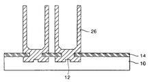
- the etch-back process removes the plugging material 22 and the molding oxide layer 16 by employing an etch selectivity ratio between the oxide layer and the polysilicon and produces a cylindrical storage node 26 .
- One storage node isolation method is a lift-off method that removes the plugged oxide layer remaining inside of the hole 18 by employing an etchant solution consisting of hydrogen fluoride (HF).
- HF hydrogen fluoride
- the HF etchant etches not only the plugged oxide layer but it also etches the interlayer insulator 10 underlying the etch stopping layer 14 , in the edge areas of a wafer.
- defects such as bridge defects are generated as the next process steps are performed on the wafer.
- Such defects may lead to failure in driving the semiconductor device, such as twin-bit failure in electrical die sorting EDS tests, which decreases the reliability of the final semiconductor devices.
- Another method of storage node isolation employs a flowable oxide as the plugging material inside of the hole 18 and isolates the storage node by a chemical-mechanical polishing (CMP) process.
- CMP chemical-mechanical polishing
- the CMP process changes the surface morphology of a wafer and produces non-uniform heights of the storage nodes between cells or chips because of micro scratches, which also result in lowering device reliability.
- the present invention provides a method of manufacturing a cylindrical storage node of a semiconductor device that minimizes a loss difference of the conductive layer, between the center and the edge areas of a cell, caused by an etch-back process of storage node isolation.
- the method of manufacturing a cylindrical storage node of a semiconductor device according to the present invention maintains uniform electrical capacitances over the entire cell areas of a wafer, which results in improved reliability of the semiconductor device.
- a method of manufacturing a cylindrical storage node in a semiconductor device comprising forming a plurality of holes in a molding insulator on cell areas, etching an etch stopping layer at the bottom of each hole and exposing a poly plug, depositing a conductive layer of a uniform thickness on the molding insulator having the plurality of holes, filling a plugging material on the conductive layer deposited on the plurality of holes, removing an upper portion of the plugging material by an etchback process to expose an upper portion of the molding insulator and the conductive layer in surrounding areas of each hole, removing the conductive layer exposed in surrounding areas of each hole to isolate the conductive layer in each hole from the conductive layer in other holes, removing the plugging material from each hole, and removing the remaining molding insulator.
- a method of manufacturing a cylindrical storage node in a semiconductor device comprising forming a plurality of holes in a molding insulator on cell areas, etching an etch stopping layer at the bottom of each hole and exposing a poly plug, depositing a conductive layer of a uniform thickness on the molding insulator having the plurality of holes, filling a plugging material, which is an oxide layer, on the conductive layer deposited on the plurality of holes, removing an upper portion of the plugging material by a wet etch process to expose an upper portion of the molding insulator and the conductive layer in surrounding areas of each hole, removing the conductive layer exposed in surrounding areas of each hole to isolate the conductive layer in each hole from the conductive layer in other holes, removing the plugging material from each hole, and removing the remaining molding insulator.
- the plugging material is a photoresist which can be etched during the etch-back process by a mixed gas of oxygen and nitrogen as a reactive gas.
- the plugging material is an oxide layer, which is one of undoped silicate glass (USG), a boron-phosphorus-silicate glass (BPSG), a silicate on glass (SOG), and a flowable oxide.
- the oxide layer can be etched during the etch-back process by reactive gas mixtures such as CHF 3 /CO/Ar or C 5 F 8 /O 2 /Ar to utilize C—C, CFx radicals that etch the oxide layer selectively, or by a wet etch process involving a solution containing HF.
- reactive gas mixtures such as CHF 3 /CO/Ar or C 5 F 8 /O 2 /Ar to utilize C—C, CFx radicals that etch the oxide layer selectively, or by a wet etch process involving a solution containing HF.
- the etchant used for removing the exposed conductive layer is a main gas SF 6 and an additional gas Cl 2 or O 2 that performs an isotropic etch to the exposed conductive layer.
- the plugging material remaining inside of the multiple holes is removed by an ashing process or a wet etch process.
- FIGS. 1-4 are cross-sectional drawings of a semiconductor device sequentially illustrating a conventional method of manufacturing a cylindrical storage node
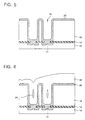
- FIGS. 5-9 are cross-sectional drawings of a semiconductor device sequentially illustrating a method of manufacturing a cylindrical storage node in a semiconductor device according to the present invention.
- FIGS. 5-9 are cross-sectional drawings of a semiconductor device sequentially illustrating a method of manufacturing a cylindrical storage node in a semiconductor device according to the present invention.
- an interlayer insulator 10 is deposited, a poly plug 12 for a bit line contact BC is formed on the interlayer insulator 10 , and a nitride layer is deposited as an etch stopping layer 14 .
- a molding oxide layer 16 is then deposited on the nitride layer 14 , and the hole 18 is produced in the molding oxide layer 16 using a photolithography and an etching process.
- the etchback process removes the nitride layer exposed at the bottom of the hole 18 and then the poly plug 12 is exposed.
- a storage conductive layer 20 is deposited to a uniform thickness.
- a plugging material 22 such as a photoresist, chemical vapor deposition CVD oxide layer, or a flowable oxide layer, is deposited.
- the CVD oxide layer includes a high temperature undoped silicate glass (USG), boron-phosphorous-silicate glass (BPSG), silicate on glass (SOG).
- the plugging material 22 prevents the bottom of the hole in the storage node from being etched during an etchback process intended for isolating the storage node.
- the deposited plugging material 22 in the cell surrounding areas, without the hole 18 underneath, is higher than that in the center of cell areas within the hole 18 by between about 2,500 to 3,000 ⁇ .
- the etchback process employs a reactive gas mixture of oxygen and nitrogen so that an etch rate in the cell surrounding areas is faster than that in the center of the cell areas in the case that the plugging material 22 is a photoresist.
- the etchback process etches the photoresist until the etchback process time reaches an endpoint where the photoresist in the cell surrounding areas is removed completely and the plugging photoresist material 22 remain only inside of the hole 18 .
- the etchback process employs a reactive gas with a high etching selectivity ratio, for example CHF 3 /CO/Ar or C 5 F 8 /O 2 Ar, between a polysilicon and the oxide layer. Therefore, the etchback process removes the plugging material 22 by using C—C or CFx radical and only the plugging material 22 inside of the hole 18 remains.
- a reactive gas with a high etching selectivity ratio for example CHF 3 /CO/Ar or C 5 F 8 /O 2 Ar
- a wet etch method employing an etching solution containing HF for example the commercial product LAL200 (manufactured by Stellar, Japan), is used for removing the upper portion of the plugging oxide layer 22 except the oxide layer inside of the hole 18 .
- the wet etching process exposes the upper portion of the molding insulator 16 and the conductive layer 20 in the surrounding areas of the multiple holes.
- overetch amounts are determined within 50%, and more preferable overetch amounts are determined within 10%, because the excess overetch amounts in a wet etch process can expose the polysilicon at the bottom of the hole 18 in the case that the plugging material 22 has voids 24 as illustrated in FIG. 7 .
- Such an excess overetch process often causes etching of the polysilicon 12 exposed at the bottom of the hole 18 , during the polysilicon etchback process of the surrounding areas, generating a bad chip.
- the polysilicon etchback process performs an isotropic etch to the exposed polysilicon 12 except to the polysilicon inside of the hole 18 , by employing a main gas SF 6 with an additional gas Cl 2 or O 2 , and isolates the storage conductive layer 20 of one hole from that of the other holes.
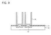
- the plugging material 22 remaining inside of the hole 18 is removed in an ashing process or a wet etch process, and finally, the molding oxide layer 16 is removed, and a cylindrical storage conductive node 26 is thereby obtained.
- the height loss of the storage conductive node according to the present invention is within about 1,000 ⁇ , so that the memory device according to the present invention can preserve more sufficient cell capacitances than the conventional memory device.
- the present invention minimizes loss differences of the cylindrical storage node 26 between the center and the edge regions of cell areas caused by an etch-back process of storage node isolation in manufacturing a semiconductor device. Then, the cylindrical storage node manufacturing method according to the present invention maintains an uniform electric capacitance over the entire cell areas of a wafer, which results in an improved device reliability.
Landscapes
- Engineering & Computer Science (AREA)
- Power Engineering (AREA)
- Computer Hardware Design (AREA)
- Microelectronics & Electronic Packaging (AREA)
- Semiconductor Memories (AREA)
- Drying Of Semiconductors (AREA)
Applications Claiming Priority (2)
| Application Number | Priority Date | Filing Date | Title |
|---|---|---|---|
| KR10-2000-0063415A KR100368935B1 (ko) | 2000-10-27 | 2000-10-27 | 반도체 장치의 실린더형 스토리지 노드 형성방법 |
| KR2000-63415 | 2000-10-27 |
Publications (2)
| Publication Number | Publication Date |
|---|---|
| US20020052089A1 US20020052089A1 (en) | 2002-05-02 |
| US6451663B1 true US6451663B1 (en) | 2002-09-17 |
Family
ID=19695737
Family Applications (1)
| Application Number | Title | Priority Date | Filing Date |
|---|---|---|---|
| US09/983,348 Expired - Fee Related US6451663B1 (en) | 2000-10-27 | 2001-10-24 | Method of manufacturing a cylindrical storage node in a semiconductor device |
Country Status (3)
| Country | Link |
|---|---|
| US (1) | US6451663B1 (ja) |
| JP (1) | JP2002151600A (ja) |
| KR (1) | KR100368935B1 (ja) |
Cited By (6)
| Publication number | Priority date | Publication date | Assignee | Title |
|---|---|---|---|---|
| US20060073669A1 (en) * | 2004-10-06 | 2006-04-06 | Shin-Hye Kim | Method of manufacturing a semiconductor device |
| US20060134875A1 (en) * | 2004-12-17 | 2006-06-22 | Samsung Electronics Co., Ltd. | Method of forming storage node of capacitor |
| US20070056930A1 (en) * | 2005-09-14 | 2007-03-15 | International Business Machines Corporation | Polysilicon etching methods |
| US7588677B2 (en) | 2000-08-30 | 2009-09-15 | Micron Technology, Inc. | Methods and apparatus for electrical, mechanical and/or chemical removal of conductive material from a microelectronic substrate |
| US7670466B2 (en) | 2004-02-20 | 2010-03-02 | Micron Technology, Inc. | Methods and apparatuses for electrochemical-mechanical polishing |
| US7700436B2 (en) * | 2002-08-29 | 2010-04-20 | Micron Technology, Inc. | Method for forming a microelectronic structure having a conductive material and a fill material with a hardness of 0.04 GPA or higher within an aperture |
Families Citing this family (6)
| Publication number | Priority date | Publication date | Assignee | Title |
|---|---|---|---|---|
| KR100475273B1 (ko) * | 2002-07-09 | 2005-03-10 | 주식회사 하이닉스반도체 | 반도체소자의 저장전극 형성방법 |
| KR100479606B1 (ko) * | 2002-07-19 | 2005-03-30 | 주식회사 하이닉스반도체 | 반도체장치의 캐패시터 제조방법 |
| KR100464859B1 (ko) * | 2003-02-26 | 2005-01-06 | 삼성전자주식회사 | 스핀온글래스 조성물을 이용한 캐패시터 형성 방법 |
| JP4908748B2 (ja) * | 2003-09-22 | 2012-04-04 | 三星電子株式会社 | 半導体素子を製造するためのエッチング方法 |
| JP2009278098A (ja) * | 2008-05-13 | 2009-11-26 | Hynix Semiconductor Inc | フラッシュメモリ素子及びその製造方法 |
| CN104465495B (zh) * | 2013-09-24 | 2017-11-03 | 中芯国际集成电路制造(上海)有限公司 | 硅通孔的形成方法 |
Citations (11)
| Publication number | Priority date | Publication date | Assignee | Title |
|---|---|---|---|---|
| US5150276A (en) * | 1992-01-24 | 1992-09-22 | Micron Technology, Inc. | Method of fabricating a vertical parallel cell capacitor having a storage node capacitor plate comprising a center fin effecting electrical communication between itself and parallel annular rings |
| US5164881A (en) * | 1991-01-30 | 1992-11-17 | Samsung Electronics Co., Ltd. | Highly integrated semiconductor memory device and the fabrication method thereof |
| US5389568A (en) * | 1992-10-29 | 1995-02-14 | Samsung Electronics Co., Ltd. | Method of making a dynamic random access memory device |
| US5573968A (en) * | 1995-02-27 | 1996-11-12 | Hyundai Electronics Industries Co., Ltd. | Method for fabricating stacked capacitors of semiconductor device |
| US5620918A (en) * | 1995-04-28 | 1997-04-15 | Nec Corporation | Method of producing cylindrical storage node of capacitor on semiconductor substrate |
| US5702974A (en) * | 1994-07-18 | 1997-12-30 | Hyundai Electronics Industries Co., Ltd. | Method for fabricating capacitor of semiconductor device |
| JPH1050951A (ja) * | 1996-07-30 | 1998-02-20 | Nec Corp | 半導体装置およびその製造方法 |
| JPH10289981A (ja) * | 1997-04-11 | 1998-10-27 | Sony Corp | 半導体記憶装置の製造方法 |
| JPH11238852A (ja) * | 1998-02-24 | 1999-08-31 | Oki Electric Ind Co Ltd | 半導体装置のキャパシタ及びその製造方法 |
| US6031262A (en) * | 1996-11-14 | 2000-02-29 | Nec Corporation | Semiconductor memory device having capacitor-over-bitline cell with multiple cylindrical storage electrode offset from node contact and process of fabrication thereof |
| US6323100B1 (en) * | 1997-05-12 | 2001-11-27 | Nec Corporation | Method for manufacturing a semiconductor device |
Family Cites Families (5)
| Publication number | Priority date | Publication date | Assignee | Title |
|---|---|---|---|---|
| KR960012257B1 (ko) * | 1993-02-12 | 1996-09-18 | 엘지반도체 주식회사 | 반도체 장치의 캐패시터 노드 제조방법 |
| KR970003922A (ko) * | 1995-06-30 | 1997-01-29 | 김주용 | 캐패시터의 전하저장전극 형성방법 |
| KR100218338B1 (ko) * | 1996-12-05 | 1999-09-01 | 구본준 | 실린더형 캐패시터 제조방법 |
| KR19990061112A (ko) * | 1997-12-31 | 1999-07-26 | 김영환 | 반도체 소자의 캐패시터 형성방법 |
| JP2000216356A (ja) * | 1999-01-21 | 2000-08-04 | Nec Corp | 半導体装置およびその製造方法 |
-
2000
- 2000-10-27 KR KR10-2000-0063415A patent/KR100368935B1/ko not_active IP Right Cessation
-
2001
- 2001-10-24 US US09/983,348 patent/US6451663B1/en not_active Expired - Fee Related
- 2001-10-26 JP JP2001329912A patent/JP2002151600A/ja active Pending
Patent Citations (11)
| Publication number | Priority date | Publication date | Assignee | Title |
|---|---|---|---|---|
| US5164881A (en) * | 1991-01-30 | 1992-11-17 | Samsung Electronics Co., Ltd. | Highly integrated semiconductor memory device and the fabrication method thereof |
| US5150276A (en) * | 1992-01-24 | 1992-09-22 | Micron Technology, Inc. | Method of fabricating a vertical parallel cell capacitor having a storage node capacitor plate comprising a center fin effecting electrical communication between itself and parallel annular rings |
| US5389568A (en) * | 1992-10-29 | 1995-02-14 | Samsung Electronics Co., Ltd. | Method of making a dynamic random access memory device |
| US5702974A (en) * | 1994-07-18 | 1997-12-30 | Hyundai Electronics Industries Co., Ltd. | Method for fabricating capacitor of semiconductor device |
| US5573968A (en) * | 1995-02-27 | 1996-11-12 | Hyundai Electronics Industries Co., Ltd. | Method for fabricating stacked capacitors of semiconductor device |
| US5620918A (en) * | 1995-04-28 | 1997-04-15 | Nec Corporation | Method of producing cylindrical storage node of capacitor on semiconductor substrate |
| JPH1050951A (ja) * | 1996-07-30 | 1998-02-20 | Nec Corp | 半導体装置およびその製造方法 |
| US6031262A (en) * | 1996-11-14 | 2000-02-29 | Nec Corporation | Semiconductor memory device having capacitor-over-bitline cell with multiple cylindrical storage electrode offset from node contact and process of fabrication thereof |
| JPH10289981A (ja) * | 1997-04-11 | 1998-10-27 | Sony Corp | 半導体記憶装置の製造方法 |
| US6323100B1 (en) * | 1997-05-12 | 2001-11-27 | Nec Corporation | Method for manufacturing a semiconductor device |
| JPH11238852A (ja) * | 1998-02-24 | 1999-08-31 | Oki Electric Ind Co Ltd | 半導体装置のキャパシタ及びその製造方法 |
Cited By (11)
| Publication number | Priority date | Publication date | Assignee | Title |
|---|---|---|---|---|
| US7588677B2 (en) | 2000-08-30 | 2009-09-15 | Micron Technology, Inc. | Methods and apparatus for electrical, mechanical and/or chemical removal of conductive material from a microelectronic substrate |
| US7700436B2 (en) * | 2002-08-29 | 2010-04-20 | Micron Technology, Inc. | Method for forming a microelectronic structure having a conductive material and a fill material with a hardness of 0.04 GPA or higher within an aperture |
| US20100176083A1 (en) * | 2002-08-29 | 2010-07-15 | Micron Technology, Inc. | Method and apparatus for removing adjacent conductive and non-conductive materials of a microelectronic substrate |
| US8048756B2 (en) | 2002-08-29 | 2011-11-01 | Micron Technology, Inc. | Method for removing metal layers formed outside an aperture of a BPSG layer utilizing multiple etching processes including electrochemical-mechanical polishing |
| US7670466B2 (en) | 2004-02-20 | 2010-03-02 | Micron Technology, Inc. | Methods and apparatuses for electrochemical-mechanical polishing |
| US20100116685A1 (en) * | 2004-02-20 | 2010-05-13 | Micron Technology, Inc. | Methods and apparatuses for electrochemical-mechanical polishing |
| US8101060B2 (en) | 2004-02-20 | 2012-01-24 | Round Rock Research, Llc | Methods and apparatuses for electrochemical-mechanical polishing |
| US20060073669A1 (en) * | 2004-10-06 | 2006-04-06 | Shin-Hye Kim | Method of manufacturing a semiconductor device |
| US7439150B2 (en) * | 2004-10-06 | 2008-10-21 | Samsung Electronics Co., Ltd. | Method of manufacturing a semiconductor device |
| US20060134875A1 (en) * | 2004-12-17 | 2006-06-22 | Samsung Electronics Co., Ltd. | Method of forming storage node of capacitor |
| US20070056930A1 (en) * | 2005-09-14 | 2007-03-15 | International Business Machines Corporation | Polysilicon etching methods |
Also Published As
| Publication number | Publication date |
|---|---|
| KR20020032773A (ko) | 2002-05-04 |
| US20020052089A1 (en) | 2002-05-02 |
| JP2002151600A (ja) | 2002-05-24 |
| KR100368935B1 (ko) | 2003-01-24 |
Similar Documents
| Publication | Publication Date | Title |
|---|---|---|
| US7307305B2 (en) | Semiconductor device | |
| US6204161B1 (en) | Self aligned contact pad in a semiconductor device and method for forming the same | |
| US8941165B2 (en) | Methods of fabricating integrated circuit capacitors having u-shaped lower capacitor electrodes | |
| US20050263814A1 (en) | Bottom electrode of capacitor of semiconductor device and method of forming the same | |
| KR100319560B1 (ko) | 물리 화학적 연마(cmp) 저지막을 사용한 커패시터 스토리지 전극 형성 방법 | |
| JP2004104098A (ja) | 低温原子層蒸着による窒化膜をエッチング阻止層として利用する半導体素子及びその製造方法 | |
| US6548853B1 (en) | Cylindrical capacitors having a stepped sidewall and methods for fabricating the same | |
| US6974993B2 (en) | Double-sided capacitor structure for a semiconductor device and a method for forming the structure | |
| KR100360739B1 (ko) | 트렌치 캐패시터 및 반도체 트랜지스터 구조체와 그 형성 방법 | |
| US6451663B1 (en) | Method of manufacturing a cylindrical storage node in a semiconductor device | |
| US20060263971A1 (en) | Semiconductor device and method thereof | |
| KR100650632B1 (ko) | 캐패시터의 제조 방법 및 이를 이용한 반도체 장치의 제조방법 | |
| US6403431B1 (en) | Method of forming in an insulating layer a trench that exceeds the photolithographic resolution limits | |
| US6238968B1 (en) | Methods of forming integrated circuit capacitors having protected layers of HSG silicon therein | |
| US7122467B2 (en) | Method for fabricating semiconductor device | |
| KR20020018025A (ko) | 반도체 장치 및 그 제조 방법 | |
| US20050014330A1 (en) | Method of planarizing an interlayer dielectric layer | |
| KR20020002898A (ko) | 반도체메모리장치의 스토리지노드 전극 제조방법 | |
| US7074725B2 (en) | Method for forming a storage node of a capacitor | |
| KR100596845B1 (ko) | 반도체 소자의 콘택 형성 방법 | |
| US6238970B1 (en) | Method for fabricating a DRAM cell capacitor including etching upper conductive layer with etching byproduct forming an etch barrier on the conductive pattern | |
| TWI833380B (zh) | 形成半導體結構之方法 | |
| US20040137680A1 (en) | Manufacturing method of semiconductor device | |
| KR100674894B1 (ko) | 2단계 화학기계적 연마를 통한 하부전극층 분리방법 | |
| KR20070031503A (ko) | 실린더형 커패시터 및 이의 제조 방법 |
Legal Events
| Date | Code | Title | Description |
|---|---|---|---|
| AS | Assignment |
Owner name: SAMSUNG ELECTRONICS CO., LTD., KOREA, REPUBLIC OF Free format text: ASSIGNMENT OF ASSIGNORS INTEREST;ASSIGNORS:CHOI, SUNG-GIL;AHN, TAE-HYUK;JEONG, SANG SUP;AND OTHERS;REEL/FRAME:012283/0333;SIGNING DATES FROM 20011012 TO 20011015 |
|
| FEPP | Fee payment procedure |
Free format text: PAYOR NUMBER ASSIGNED (ORIGINAL EVENT CODE: ASPN); ENTITY STATUS OF PATENT OWNER: LARGE ENTITY |
|
| FPAY | Fee payment |
Year of fee payment: 4 |
|
| REMI | Maintenance fee reminder mailed | ||
| LAPS | Lapse for failure to pay maintenance fees | ||
| STCH | Information on status: patent discontinuation |
Free format text: PATENT EXPIRED DUE TO NONPAYMENT OF MAINTENANCE FEES UNDER 37 CFR 1.362 |
|
| FP | Lapsed due to failure to pay maintenance fee |
Effective date: 20100917 |