US6411554B1 - High voltage switch circuit having transistors and semiconductor memory device provided with the same - Google Patents
High voltage switch circuit having transistors and semiconductor memory device provided with the same Download PDFInfo
- Publication number
- US6411554B1 US6411554B1 US09/710,909 US71090900A US6411554B1 US 6411554 B1 US6411554 B1 US 6411554B1 US 71090900 A US71090900 A US 71090900A US 6411554 B1 US6411554 B1 US 6411554B1
- Authority
- US
- United States
- Prior art keywords
- voltage
- node
- high voltage
- power supply
- level
- Prior art date
- Legal status (The legal status is an assumption and is not a legal conclusion. Google has not performed a legal analysis and makes no representation as to the accuracy of the status listed.)
- Expired - Fee Related
Links
Images


Classifications
-
- G—PHYSICS
- G11—INFORMATION STORAGE
- G11C—STATIC STORES
- G11C11/00—Digital stores characterised by the use of particular electric or magnetic storage elements; Storage elements therefor
- G11C11/21—Digital stores characterised by the use of particular electric or magnetic storage elements; Storage elements therefor using electric elements
- G11C11/34—Digital stores characterised by the use of particular electric or magnetic storage elements; Storage elements therefor using electric elements using semiconductor devices
- G11C11/40—Digital stores characterised by the use of particular electric or magnetic storage elements; Storage elements therefor using electric elements using semiconductor devices using transistors
-
- G—PHYSICS
- G11—INFORMATION STORAGE
- G11C—STATIC STORES
- G11C5/00—Details of stores covered by group G11C11/00
- G11C5/14—Power supply arrangements, e.g. power down, chip selection or deselection, layout of wirings or power grids, or multiple supply levels
- G11C5/145—Applications of charge pumps; Boosted voltage circuits; Clamp circuits therefor
-
- G—PHYSICS
- G11—INFORMATION STORAGE
- G11C—STATIC STORES
- G11C16/00—Erasable programmable read-only memories
- G11C16/02—Erasable programmable read-only memories electrically programmable
- G11C16/06—Auxiliary circuits, e.g. for writing into memory
- G11C16/30—Power supply circuits
-
- G—PHYSICS
- G11—INFORMATION STORAGE
- G11C—STATIC STORES
- G11C8/00—Arrangements for selecting an address in a digital store
- G11C8/08—Word line control circuits, e.g. drivers, boosters, pull-up circuits, pull-down circuits, precharging circuits, for word lines
Definitions
- the present invention relates to a high voltage switch circuit and a semiconductor memory device provided with the same and, more particularly to a structure performing voltage control and ensuring a normal switching operation.
- a high voltage switch circuit has been used as a circuit for converting the amplitude level of an input signal.
- the high voltage switch circuit converts an input signal (amplitude level VCC ⁇ GND) switching between a power supply voltage level VCC and a ground voltage level GND to a signal (amplitude level VPP ⁇ GND) switching between a positive high voltage level VPP and a ground voltage level GND or to a signal (amplitude level VN ⁇ VCC) switching between a negative high voltage level VN and power supply voltage level VCC (
- the high voltage switch circuit includes a transistor (a switching transistor) for switching and a transistor for voltage control.
- a high voltage is applied between the source and drain of the switching transistor during the switching operation, during which hot carriers are generated to cause degradation of the current value or threshold value of the transistor.
- the transistor for voltage control is arranged to control the voltage of the transistor.
- Such a high voltage switch circuit is used for controlling data writing, reading, erasing and the like, with respect to a memory cell of the semiconductor memory device.
- a gate voltage of the transistor for voltage control is fixed at a prescribed value (at power supply voltage VCC when switching at high voltage VPP and at ground voltage GND when switching at high voltage VN).
- the conventional structure suffers from a problem that the circuit cannot operate if the switching high voltage is close to power supply voltage VCC or ground voltage GND.
- a memory operation must be controlled by using a high voltage switch circuit ensuring a normal switching operation and optimum voltage control.
- the present invention provides a high voltage switch circuit ensuring a normal switching operation and optimum voltage control as well as a semiconductor memory device provided with the same.
- a high voltage switch circuit includes: a first power supply node capable of supplying a high voltage greater in absolute value than a power supply voltage; a second power supply node to supply a voltage at most the power supply voltage; a first transistor converting the voltage level of an input signal in accordance with the input signal and the voltage supplied from the first power supply node; a second transistor converting the voltage level of an input signal in accordance with the input signal and the voltage supplied from the second power supply node; a switch circuit switching the amplitude level of an input signal between the power supply voltage level and the ground voltage level; and a third transistor connected between the first and second transistors and having its gate voltage controlled.
- the third transistor operates such that the drain-source voltage of the first or second transistors is controlled.
- the gate voltage of the third transistor is switched by a control signal for making the first power supply node attain to a high voltage.
- the voltage of the first power supply node attains to a high voltage when a first period of time is elapsed after it is at a power supply voltage.
- the gate voltage of the third transistor is switched by a signal activated when a second period of time shorter than the first period of time is elapsed after the voltage of the first power supply node begins to change.
- the gate voltage of the third transistor is switched by a signal activated when the voltage of the first power supply node attains to a prescribed level.
- the gate voltage of the third transistor is controlled by a control signal at a voltage level which is less dependent on the power supply voltage. It is noted that the above mentioned voltage may arbitrarily be changed.
- the gate of the third transistor is controlled by a bias voltage allowing a constant current which does not depend on the high voltage.
- the gate voltage of the transistor for voltage control can be controlled. Accordingly, the voltage of the transistor is controlled when the voltage of the power supply node attains to a desired high voltage level. In addition, a normal operation is ensured even if the power supply node is at the low voltage level.
- the gate voltage of the transistor for voltage control can be controlled by a control signal for making the voltage level of the power supply node attain to the high voltage level.
- the gate voltage of the transistor for voltage control can be controlled by a signal activated when the voltage level of the power supply node increases or decreases.
- the gate voltage of the transistor for voltage control can be controlled by a signal activated when the voltage of the power supply node attains to a desired level.
- the gate voltage of the transistor for voltage control can be controlled by a signal which is not dependent or less dependent on the power supply voltage.
- a semiconductor memory device includes: a memory cell array including a plurality of memory cells; a control circuit for controlling the operation of the memory cell array; a circuit generating an operation signal for operating the memory cell array under control of the control circuit; a generation circuit outputting a power supply voltage in a stand-by mode and activated during the operation of the memory cell array for generating a high voltage greater in absolute value than the power supply voltage; and a high voltage switch circuit switching the amplitude level of the operation signal.
- the high voltage switch circuit includes: a first power supply node receiving a voltage output from the generation circuit; a second power supply node supplied with a voltage at most the power supply voltage; a first transistor converting the voltage level of the operation signal in accordance with the operation signal and the voltage supplied from the first power supply node; a second transistor converting the voltage level of the operation signal in accordance with the operation signal and the voltage supplied from the second power supply node; a switch circuit switching the amplitude level of the operation signal; and a third transistor connected between the first and second transistors and having its gate voltage controlled.
- the third transistor operates such that a drain-source voltage of the first or second transistors is controlled.
- control circuit includes a circuit generating a control signal for activating the generation circuit, and the gate voltage of the third transistor is switched by the control signal.
- control circuit includes a circuit generating a control signal for activating the generation circuit and a delay circuit for delaying the control signal by a prescribed period of time for output.
- the gate voltage of the third transistor is switched by an output from the delay circuit.
- control circuit includes a circuit generating a control signal for activating the generation circuit and a circuit generating a detection signal which is activated when an output from the generation circuit attains to a prescribed level.
- the gate voltage of the third transistor is switched by the detection signal.
- the operation signal switches between the power supply voltage and the ground voltage.
- the control circuit includes a signal generation circuit generating a control signal at a voltage level which is less dependent on the power supply voltage.
- the gate voltage of the third transistor is switched by the control signal. It is noted that the above defined voltage may arbitrarily be changed by the signal generation circuit.
- the operation signal switches between the power supply voltage and the ground voltage.
- the control circuit includes a circuit generating a bias voltage to be supplied to the gate of the third transistor such that a constant current, which is not dependent on the high voltage, flows to the third transistor.
- the gate voltage of the transistor for voltage control can be controlled in the high voltage switch circuit switching the voltage level of the operation signal for the memory operation. Accordingly, voltage control is achieved in accordance with the memory operation, thereby enabling a normal operation if the memory operation is performed or not.
- the gate voltage of the transistor for voltage control can be controlled by a control signal activating the circuit generating the high voltage.
- the gate voltage of the transistor for voltage control can be controlled by a signal obtained by delaying the control signal activating the circuit generating the high voltage.
- the gate voltage of the transistor for voltage control can be controlled by a signal activated when the voltage output from the circuit generating the high voltage during the operation of the memory cell array attains to a prescribed level.
- the gate voltage of the transistor for voltage control can be controlled by a signal at a voltage level which is not dependent or less dependent on the power supply voltage.
- the semiconductor memory device of the present invention a normal operation and voltage control of the high voltage switch circuit are ensured, so that an accurate operation is ensured.
- FIG. 1 is a diagram shown in conjunction with a high voltage switch circuit 2 according to the first embodiment of the present invention.
- FIG. 2 is a diagram schematically showing an overall arrangement of a semiconductor memory device 1000 including high voltage switch circuit 2 according to the first embodiment.
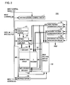
- FIG. 3 is a timing chart shown in conjunction with a control method for high voltage switch circuit 2 according to the first embodiment.
- FIG. 4 is a timing chart shown in conjunction with voltage control in high voltage switch circuit 2 according to the first embodiment.
- FIGS. 5 and 6 are circuit diagrams respectively showing structures of high voltage switch circuits 2 A and 2 B.
- FIG. 7 is a diagram shown in conjunction with control of a high voltage switch circuit 2 according to the second embodiment.
- FIG. 8 is a circuit diagram exemplifying the structure of a reference voltage generation circuit 3 .
- FIG. 9 is a timing chart shown in conjunction with a control method for high voltage switch circuit 2 according to the second embodiment.
- FIG. 10 is a diagram shown in conjunction with control of a high voltage switch circuit 2 according to the third embodiment.
- FIG. 11 is circuit diagram showing the structure of a VPP detection circuit 5 .
- FIG. 12 is a timing chart shown in conjunction with a control method for a high voltage switch circuit 2 according to the third embodiment.
- FIG. 13 is a diagram shown in conjunction with control of a high voltage switch circuit 2 according to the fourth embodiment.
- FIG. 14A is a timing chart shown in conjunction with a control method for high voltage switch circuit 2 according to the fourth embodiment.
- FIG. 17 is a timing chart shown in conjunction with a control method for high voltage switch circuit 2 according to the fifth embodiment.
- FIG. 18 is a timing chart shown in conjunction with voltage control in high voltage switch circuit 2 according to the fifth embodiment.
- FIGS. 19 and 20 are circuit diagrams exemplifying the structure of variable resistors.
- FIG. 21 is a diagram shown in conjunction with control of a high voltage switch circuit 8 according to the sixth embodiment.
- FIG. 22 is a circuit diagram showing the structure of a VN detection circuit 9 .
- FIG. 23 is a timing chart shown in conjunction with a control method for high voltage switch circuit 8 according to the sixth embodiment.
- FIG. 24 is a timing chart shown in conjunction with voltage control in high voltage switch circuit 8 according to the sixth embodiment.
- FIGS. 25 and 26 are circuit diagrams respectively showing the structures of high voltage switch circuits 8 A and 8 B.
- FIG. 27 is a diagram shown in conjunction with control of a high voltage switch circuit 2 according to the seventh embodiment.
- FIG. 28 is a timing chart shown in conjunction with a control method for high voltage switch circuit 2 according to the seventh embodiment.
- FIG. 29 is a timing chart shown in conjunction with voltage control in high voltage switch circuit 2 according to the seventh embodiment.
- FIG. 30 is a circuit diagram exemplifying a high voltage switch circuit 900 including a voltage control circuit.
- FIG. 31 is a circuit diagram showing the structures of a VPP detection circuit 5 A according to the eighth embodiment.
- a high voltage switch circuit 2 converts an input signal VIN (amplitude VCC ⁇ GND) to a signal VOUT (amplitude VPP ⁇ GND) and, as shown in FIG. 1, includes transistors Q 1 to Q 6 as well as an inverter IV 0 .
- Transistors Q 1 to Q 4 are PMOS transistors, whereas transistors Q 5 and Q 6 are NMOS transistors.
- Transistor Q 5 is connected between a node N 3 and a node GND receiving a ground voltage GND and has its gate receiving input signal VIN.
- Inverter IV 0 inverts and outputs input signal VIN.
- Transistor Q 6 is connected between nodes OUT and GND and has its gate receiving an output from inverter IV 0 .
- Transistor Q 3 is connected between nodes N 1 and N 3 , whereas transistor Q 4 is connected between nodes N 2 and OUT.
- Transistor Q 1 is connected between a node VPP receiving a high voltage and node N 1 and has its gate connected to node OUT.
- Transistor Q 2 is connected between nodes VPP and N 2 and has its gate connected to node N 3 .
- Transistors Q 3 and Q 4 are transistors for voltage control and form a voltage control circuit 10 for controlling the gate voltage of the transistor of the circuit. Unlike the conventional case, the gates of transistors for voltage control Q 3 and Q 4 are not supplied with a prescribed voltage, but receive externally input gate control signal A.
- gate control signal A is controlled by a writing/erasing control circuit 1 for controlling writing/erasing with respect to the memory cell.
- semiconductor memory device 1000 includes: a writing/erasing control circuit 1 ; an address buffer 100 externally receiving an address AD; a data input/output buffer 101 for inputting/outputting data; a memory cell array MR including a plurality of memory cells arranged in a matrix; an X decoder 102 and Y-decoder 103 for selecting an arbitrary memory cell from memory cell array MR; a well/source decoder 104 for driving well and source voltages for data writing/erasing/reading with respect to the memory cell; a sense amplifier for reading data from the memory cell; and a writing circuit for writing data.
- the sense amplifier and writing circuit are collectively depicted as a single block 105 .
- Writing/erasing control circuit 1 controls the operation of an internal circuit by an input of a control signal CNT (a chip enable signal, write enable signal and the like) received from the external portion of the chip and a dedicated data input referred to as a command CM. It is noted that dedicated command CM is determined for every chip operation such as writing/erasing/reading operation.
- CNT chip enable signal, write enable signal and the like
- Semiconductor memory device 1000 further includes: a high voltage generation circuit 106 boosting power supply voltage VCC for generating positive high voltage VPP; a negative high voltage generation circuit 107 down-converting a ground voltage GND for generating a negative high voltage VN; a reference voltage generation circuit 108 generating a reference voltage VREF used for control of the voltage level; and a high voltage switch circuit 120 converting and outputting the amplitude level of a signal (input signal VIN) received from address buffer 100 in accordance with a signal from writing/erasing control circuit 1 .
- a high voltage generation circuit 106 boosting power supply voltage VCC for generating positive high voltage VPP
- a negative high voltage generation circuit 107 down-converting a ground voltage GND for generating a negative high voltage VN
- a reference voltage generation circuit 108 generating a reference voltage VREF used for control of the voltage level
- a high voltage switch circuit 120 converting and outputting the amplitude level of a signal (input signal VIN) received from address buffer 100
- High voltage VPP and negative high voltage VN respectively output from high voltage generation circuit 106 and negative high voltage generation circuit 107 are used for data writing/erasing/reading with respect to the memory cell.
- High voltage switching circuit 120 converts and outputs the amplitude level of input signal VIN from a level between VCC and GND to that between VPP and GND or between VCC and VN for controlling a circuit (X decoder 102 , Y decoder 103 , well/source decoder 104 ) to which a high voltage is applied during the writing/erasing/reading operation.
- the above mentioned high voltage switch circuit 2 is included in high voltage switch circuit 120 .
- writing/erasing control circuit 1 When command CM designating the specific operation is input, writing/erasing control circuit 1 outputs a prescribed control signal. High voltage generation circuit 106 , negative high voltage generation circuit 107 and reference voltage generation circuit 108 are activated/inactivated under control of writing/erasing control circuit 1 .
- high voltage generation circuit 106 When high voltage generation circuit 106 is activated, the voltage output from high voltage generation circuit 106 attains to a prescribed high voltage level VPP from power supply voltage level VCC. When negative high voltage generation circuit 107 is activated, the voltage output from negative high voltage generation circuit 107 attains to a prescribed negative high voltage level VN from ground voltage level GND.
- high voltage generation circuit 106 and negative high voltage generation circuit 107 are independently controlled by writing/erasing control circuit 1 . Accordingly, activation/inactivation timings of high voltage generation circuit 106 and negative high voltage generation circuit 107 are independent of each other. It is noted that high voltage switch circuit 2 receives an output from high voltage generation circuit 106 at node VPP.
- high voltage switch circuit 900 of which method of controlling the transistor for voltage control is different from that of high voltage switch circuit 2 will be described.
- High voltage switch circuit 900 shown in FIG. 30 converts input signal VIN (amplitude VCC ⁇ GND) to signal VOUT (amplitude VPP ⁇ GND) and includes transistors Q 91 to Q 96 as well as an inverter IV 90 .
- Transistors Q 91 to Q 94 are PMOS transistors, whereas transistors Q 95 and Q 96 are NMOS transistors.
- Transistor Q 95 is connected between a node N 90 and a node GND receiving a ground voltage GND and has its gate receiving input signal VIN.
- Inverter IV 90 inverts and outputs input signal VIN.
- Transistor Q 96 is connected between a node OUT, that is an output node of the circuit, and node GND, and has its gate receiving an output from inverter IV 90 .
- Transistor Q 93 is connected between transistor Q 91 and node N 90 , whereas transistor Q 94 is connected between transistor Q 92 and node OUT.
- Transistors Q 93 and Q 94 have their gates receiving power supply voltage
- transistors Q 91 and Q 92 are connected to node VPP receiving positive high voltage VPP, and transistors Q 91 and Q 92 have their gates respectively connected to node OUT and node N 90 .
- Transistors Q 93 and Q 94 (transistors for voltage control) form a voltage control circuit 910 .
- Voltage control circuit 910 controls the source-drain voltage of the transistors when switching to the high voltage.
- High voltage switch circuit 900 converts input signal VIN (amplitude level VCC ⁇ GND) to signal VOUT (amplitude level VPP ⁇ GND).
- the gate voltage of the transistor for voltage control is fixed at a prescribed voltage (power supply voltage VCC). Accordingly, the circuit operation is not ensured if the high voltage to be switched is close to power supply voltage VCC or ground voltage GND.
- gate control signal A controlling the gate of the transistor for voltage control is changed in accordance with the level of the voltage to be applied to node VPP of high voltage switch circuit 2 .
- high voltage switch circuit 2 receives input signal VIN at power supply voltage level VCC during times t 0 to t 1 and t 3 to t 4 .
- power supply voltage VCC is applied to node VPP in an initial state.
- Gate control signal A is at ground voltage level GND when power supply voltage VCC is applied to node VPP (up to t 2 ). Accordingly, input signal VIN received from time t 0 to t 1 is converted to signal VOUT at power supply voltage level VCC for output.
- gate control signal A is switched to attain from ground voltage level GND to power supply voltage level VCC.
- the voltage levels of internal nodes N 1 and N 2 in high voltage switch circuit 2 are changed as shown in FIG. 4 when switching to the high voltage.
- the source-drain voltages are controlled to ⁇ VPP ⁇ (VCC+
- Vthp represents the threshold value of transistors Q 3 and Q 4 .
- writings/erasing control circuit 1 outputs gate control signal A at ground voltage level GND.
- high voltage generation circuit 106 is in an inactive state.
- gate control signal A at power supply voltage level VCC is output from writing/erasing control circuit 1 , so that high voltage generation circuit 106 is activated.
- the level of gate control signal A is switched to ground voltage level GND to inactivate high voltage generation circuit 106 .
- the level of the voltage applied to node VPP is decreased to attain to power supply voltage level VCC.
- gate control signal A a signal directly controlling activation/inactivation of high voltage generation circuit 106 may be used as gate control signal A.
- a high voltage switch circuit 2 A shown in FIG. 5 includes transistors Q 1 , Q 2 , Q 5 and Q 6 , a voltage control circuit 10 A having transistors Q 3 , Q 4 , Q 7 and Q 8 , as well as an inverter IV 0 .
- Transistors Q 7 and Q 8 are NMOS transistors.
- transistors Q 3 , Q 4 , Q 7 and Q 8 function as transistors for voltage control.
- Transistor Q 7 is connected between transistors Q 3 and Q 5 , whereas transistor Q 8 is connected between transistors Q 4 and Q 6 .
- Each of transistors Q 7 and Q 8 has its gate receiving a power supply voltage.
- a high voltage switch circuit 2 B shown in FIG. 6 includes transistors Q 1 , Q 2 , Q 5 and Q 6 , a voltage control circuit 10 B having transistors Q 7 and Q 8 , as well as an inverter IV 0 .
- transistors Q 7 and Q 8 function as transistors for voltage control.
- Transistor Q 1 is connected between nodes VPP and N 1 and have its gate receiving a signal VOUT of node OUT.
- Transistor Q 2 is connected between nodes VPP and OUT and has its gate receiving a signal of node N 1 .
- Transistor Q 7 is connected between node N 1 and transistor Q 5 , whereas transistor Q 8 is connected between node OUT and transistor Q 6 .
- Transistors Q 7 and Q 8 have their gates receiving gate control signals A.
- a high voltage switch circuit 2 according to the second embodiment has transistors Q 3 and Q 4 that have their gates receiving gate control signals A output from an AND circuit 90 .
- AND circuit 90 has its input receiving a control signal B output from a writing/erasing control circuit 1 and an output from a timer circuit 4 .
- Timer circuit 4 outputs a signal at an H level when a prescribed period of time is elapsed after control signal B at the H level is received from writing/erasing control circuit 1 .
- Timer circuit 4 will be described.
- Timer circuit 4 includes transistors Q 20 to Q 22 , a capacitor C 1 , and an inverter IV 1 .
- Transistor Q 20 is a PMOS transistor, whereas transistors Q 21 and Q 22 are NMOS transistors.
- Transistor Q 20 is connected between a node receiving a power supply voltage and a node N 5 , whereas transistors Q 21 and Q 22 are connected in series between node N 5 and a node GND receiving a ground voltage GND.
- Transistors Q 20 , Q 22 and transistor Q 21 have their gates receiving control signal B and a reference voltage VREF output from a reference voltage generation circuit 3 , respectively.
- Capacitor C 1 is connected between nodes N 5 and GND, and inverter IV 1 inverts a signal of node N 5 for output.
- AND circuit 90 has its input receiving an output from inverter IV 1 and control signal B for outputting a gate control signal A.
- Reference voltage generation circuit 3 includes transistors Q 61 to Q 65 and resistors R 1 and R 2 , as shown in FIG. 8 .
- Transistors Q 61 , Q 62 , and Q 65 are PMOS transistors, whereas transistors Q 63 and Q 64 are NMOS transistors.
- Resistor R 1 is connected between a node VCC receiving power supply voltage VCC and a node N 60 .
- Transistors Q 61 and Q 63 are connected in series between node VCC and node GND receiving ground voltage GND.
- Transistors 62 and 64 are connected in series between nodes N 60 and GND.
- Transistors Q 63 and Q 64 form a current mirror circuit.
- Transistor Q 65 and resistor R 2 are connected in series between nodes VCC and GND, and a reference voltage VREF is output from a connection node of transistor Q 65 and resistor R 2 .
- Reference voltage VREF will be described.
- the same current is supplied to transistor Q 61 and resistor R 1 because of transistors Q 63 and Q 64 (a current mirror circuit). If a conductance and threshold value of transistor Q 61 are respectively ⁇ 1 and VthQ 1 , a current IR 1 flowing through resistor R 1 satisfies the following equation (1). Assume that resistance values of resistors R 1 and R 2 are respectively R 1 and R 2 .
- IR 1 VthQ 1 +(21/ ⁇ 1 ) (1)
- reference voltage VREF satisfying the following equation (4) is to be output.
- Control signal B is changed in accordance with the level of the voltage applied to node VPP of high voltage switch circuit 2 .
- gate control signal A is generated in accordance with control signal B and an output from timer circuit 4 .
- timer circuit 4 attains to power supply voltage level VCC delayed by a prescribed period of time (a delay time ⁇ t 1 ) with respect to the rise of control signal B.
- Delay time ⁇ t 1 is controlled by the amount of electric charges in capacitor C 1 and a current for discharging the electric charges.
- Gate control signal A is switched to attain to power supply voltage VCC level from ground voltage level GND when the voltage applied to node VPP attains to the voltage level at which voltage control is required, in accordance with the following equation (5). It is noted that, in equation (5), tr and VPP respectively represent the rising time of the high voltage and the voltage at node VPP.
- V (t) (VPP ⁇ VCC)/tr ⁇ t+VCC (5)
- control signal B is at ground voltage level GND. Accordingly, input signal VIN received between times t 0 and t 1 is converted to a signal VOUT at power supply voltage level VCC for output.
- control signal B When application of the high voltage to node VPP is started (at a time t 2 ), the level of control signal B is switched from ground voltage level GND to power supply voltage level VCC.
- gate control signal A attains to power supply voltage level VCC.
- V 0 the voltage at which voltage control is required.
- Such a control method allows control of the voltage level at internal nodes N 1 and N 2 in high voltage switch circuit 2 when switching to the high voltage.
- high voltage switch circuit 2 When application of the high voltage to node VPP is finished or when power supply voltage VCC is applied without application of the high voltage, the gate voltages of transistors for voltage control Q 3 and Q 4 are changed from power supply voltage VCC to ground voltage GND or fixed at ground voltage GND.
- high voltage switch circuit 2 enables a normal switching operation even if the level of the voltage applied to node VPP is low.
- Reference voltage generation circuit 3 is included in a reference voltage generation circuit 108 .
- writing/erasing control circuit 1 outputs control signal B at ground voltage level GND with respect to AND circuit 90 .
- high voltage generation circuit 106 is in the inactive state.
- control signal B at power supply voltage level VCC is output from writing/erasing control circuit 1 , and high voltage generation circuit 106 is activated.
- gate control signal A input to the gate of the transistor for voltage control attains to power supply voltage level VCC.
- control signal B When application of the high voltage is finished, the level of control signal B is changed to ground voltage level GND, and high voltage generation circuit 106 is inactivated. The level of the voltage applied to node VPP is decreased to attain to power supply voltage level VCC.
- Such a control method enables semiconductor memory device 1000 to perform a correct writing/erasing/reading operation. It is noted that a signal directly controlling activation/inactivation of high voltage generation circuit 106 may be used as control signal B.
- the method according to the second embodiment is not only applied to high voltage switch circuit 2 but also applicable to the above described high voltage switch circuits 2 A, 2 B and the like. Further, it can be applied to a high voltage switch circuit switching input signal VIN to signal VOUT at amplitude level VN ⁇ VCC.
- an AND circuit 90 outputs a gate control signal A in accordance with a control signal B output from writing/erasing control circuit 1 and a level detection signal C output from a VPP detection circuit 5 .
- Transistors for voltage control Q 3 and Q 4 included in high voltage switch circuit 2 have their gates receiving gate control signals A generated by control signal B and level detection signal C.
- VPP detection circuit 5 includes resistors R 1 and R 2 as well as a voltage comparison circuit 12 as shown in FIG. 11 .
- Resistors R 1 and R 2 are connected in series between a node VPP receiving a high voltage and a node GND receiving a ground voltage.
- a connection node of resistors R 1 and R 2 is connected to a positive input terminal of voltage comparison circuit 12 .
- a negative input terminal of voltage comparison circuit 12 receives a reference voltage VREF output from a reference voltage generation circuit 3 .
- VPPn VPP ⁇ R 2 /(R 1 +R 2 ) ⁇ (6)
- Voltage comparison circuit 12 compares divided voltage VPPn and reference voltage VREF for outputting level detection signal C as a comparison result.
- Resistance values R 1 and R 2 are determined to satisfy the following equation (7).
- VPP generation circuit 5 outputs level detection signal C at an H level if divided voltage VPPn exceeds reference voltage VREF, and outputs level detection signal C at an L level in all other cases.
- Control signal B is changed in accordance with the level of the voltage applied to node VPP of high voltage switch circuit 2 .
- gate control signal A is generated in accordance with control signal B and level detection signal C output from VPP detection circuit 5 .
- Level detection signal C attains to the H level when the voltage applied to node VPP exceeds a prescribed level.
- control signal B When application of the high voltage to node VPP is started (time t 2 ), the level of control signal B is changed from ground voltage level GND to power supply voltage level VCC.
- level detection signal C attains to power supply voltage level VCC from ground voltage level GND.
- Gate control signal A attains to power supply voltage level VCC from ground voltage level GND (t 2 ⁇ tx ⁇ t 3 ).
- control signal B is charged from power supply voltage level VCC to ground voltage level GND.
- Gate control signal A attains to ground voltage level GND from power supply voltage level VCC.
- level detection signal C attains to ground voltage level GND from power supply voltage level VCC.
- Such a control method enables control of the voltage level at internal nodes N 1 and N 2 in high voltage switch circuit 2 when switching to the high voltage.
- the gate of the transistor for voltage control attains to ground voltage level GND from power supply voltage level VCC or fixed at ground voltage level GND.
- writing/erasing control circuit 1 outputs control signal B at ground voltage level GND to AND circuit 90 .
- high voltage generation circuit 106 is in an inactive state.
- control signal B at power supply voltage level VCC is output from writing/erasing control circuit 1 , so that high voltage generation circuit 106 is activated.
- gate control signal A input to the gate of the transistor for voltage control attains to power supply voltage level VCC.
- control signal B attains to ground voltage level GND, so that high voltage generation circuit 106 is inactivated.
- the voltage applied to node VPP is decreased to attain to power supply voltage level VCC.
- control signal B Such control enables semiconductor memory device 1000 to perform a normal writing/erasing/reading operation. It is noted that a signal directly controlling activation/inactivation of high voltage generation circuit 106 may be used as control signal B.
- detection level V 0 may be set to have different values when the voltage increases and decreases. If the values of the detection levels are different when increasing and decreasing, resistors R 1 and R 2 of VPP detection circuit 5 would be variable resistors, so that resistance values may vary according to signals respectively output when increasing and decreasing from writing/erasing control circuit 1 .
- the method of the third embodiment is not only applied to high voltage switch circuit 2 , but is also applicable to the above described high voltage switch circuits 2 A, 2 B and the like.
- the method may also be applied to a high voltage switch circuit switching input signal VIN to signal VOUT at amplitude level VN ⁇ VCC.
- an AND circuit 90 receives an output from 1 ⁇ 2 VPP detection circuit 6 as an operation power supply voltage.
- 1 ⁇ 2 VPP detection circuit 6 will be described.
- 1 ⁇ 2 VPP detection circuit includes transistors Q 30 to Q 37 .
- Transistors Q 30 to Q 33 are PMOS transistors, whereas transistors Q 34 to Q 37 are NMOS transistors.
- Transistor Q 30 is connected between a node VPP supplied with a high voltage and a node N 10 , whereas transistor Q 34 is connected between node N 10 and a node GND receiving a ground voltage GND. Transistor Q 30 has its gate connected to node N 10 . Transistors Q 34 and Q 36 have their gates receiving a reference voltage VREF output from a reference voltage generation circuit 3 .
- Transistor Q 31 is connected between nodes VPP and N 11 and has its gate connected to node N 10 .
- Transistors Q 35 and Q 32 are connected in series between nodes N 11 and N 12 , and transistor Q 36 is connected between nodes N 12 and GND.
- Transistor Q 35 has its gate connected to node N 11
- transistor Q 32 has its gate connected to node N 12 .
- Transistor Q 37 is connected between nodes VPP and N 13 , whereas transistor Q 33 is connected between nodes N 13 and GND. Transistors Q 37 and Q 33 have their gates connected to nodes N 11 and N 12 , respectively.
- a node N 13 which is a connection node of transistors Q 33 and Q 37 , attains to a voltage level (1 ⁇ 2 VPP) which is a high voltage VPP.
- a gate control signal A controlling the gate of the transistor for voltage control is generated in accordance with a control signal B and a level detection signal C.
- gate control signal A is converted to a voltage 1 ⁇ 2 VPP which is less dependent on VCC.
- Gate control signal A attains to a 1 ⁇ 2 VPP level in a range where the voltage supplied to node VPP exceeds a detection level V 0 .
- control signal B and level detection signal C are both at ground voltage level GND.
- Gate control signal A is at ground voltage level GND. Accordingly, input signal VIN received between times t 0 and t 1 is converted to signal VOUT at power supply voltage level VCC for output.
- control signal B attains to power supply level VCC from ground voltage level GND.
- level detection signal C attains to power supply voltage level VCC from ground voltage level GND.
- Gate control signal A attains to the 1 ⁇ 2 VPP level.
- control signal B attains to ground voltage level GND from power supply voltage level VCC.
- Gate control signal A attains to ground voltage level GND.
- level detection signal attains to ground voltage level GND from power supply voltage level VCC.
- the voltage levels of internal nodes N 1 and N 2 in high voltage switch circuit 2 change as shown in FIG. 15 when switching the high voltage.
- the source-drain voltage of the PMOS transistor forming the circuit is controlled to (1 ⁇ 2 VPP+
- control method will be described as applied to semiconductor memory device 1000 .
- writing/erasing control circuit 1 outputs control signal B at ground voltage level GND.
- high voltage generation circuit 106 is in an inactive state.
- control signal B at power supply voltage level VCC is output from writing/erasing control circuit 1 , so that high voltage generation circuit 106 is activated.
- gate control signal A input to the gate of the transistor for voltage control attains to the 1 ⁇ 2 VPP level.
- control signal B attains to ground voltage level GND, so that high voltage generation circuit 106 is inactivated.
- the level of the voltage applied to node VPP is decreased to attain the power supply voltage level VCC.
- control signal B a signal directly controlling activation/inactivation of high voltage generation circuit 106 may be used as control signal B.
- the method of the fourth embodiment is not only applied to high voltage switch circuit 2 , but also applicable to the above described high voltage switch circuits 2 A, 2 B and the like.
- the method can also be applied to a high voltage switch circuit switching input signal VIN to signal VOUT at amplitude level VN ⁇ VCC.
- an AND circuit 90 receives an output from a constant voltage generation circuit 7 as an operation power supply voltage.
- Constant voltage generation circuit 7 includes transistors Q 40 to Q 45 and variable resistors Rx and Ry.
- Transistors Q 40 , Q 41 and Q 45 are PMOS transistors, whereas transistors Q 42 and Q 43 are NMOS transistors.
- Transistors Q 40 to Q 44 form a current mirror differential amplifier.
- Transistors Q 40 and Q 41 form a PMOS current mirror circuit, and transistor Q 44 functions as a constant current source.
- Transistor Q 40 is connected between a node VPP supplied with a high voltage and a node N 20 , whereas transistor Q 41 is connected between nodes VPP and N 21 .
- Transistors Q 40 and Q 41 have their gates connected to node N 21 .
- Transistor Q 42 is connected between nodes N 20 and N 22 , and transistor Q 43 is connected between nodes N 21 and N 22 .
- Transistor Q 42 has its gate receiving a reference voltage VREF output from a reference voltage generation circuit 3
- transistor Q 43 has its gate connected to a connection node of variable resistors Rx and Ry.
- Transistor Q 44 is connected between node N 22 and a node GND receiving ground voltage GND, and has its gate receiving a control signal output from a writing/erasing control circuit 1 .
- Transistor Q 45 is connected between nodes VPP and N 23 , and variable resistors Rx and Ry are connected in series between nodes N 23 and GND.
- a voltage Vconst at node N 23 satisfies the following equation (8). Assume that resistance values of variable resistors Rx and Ry are respectively Rx and Ry.
- Vconst VREF ⁇ (Rx+Ry)/Ry ⁇ (8)
- reference voltage VREF is independent of power supply voltage VCC as shown in equation (4), so that voltage Vconst is also independent of power supply voltage VCC.
- a control method for high voltage switch circuit 2 will now be described.
- a gate control signal A controlling the gate of the transistor for voltage control is generated in accordance with control signal B, level detection signal C, and control signal D.
- the voltage of gate control signal A is converted to voltage Vconst, which is not dependent on power supply voltage VCC.
- Gate control signal A attains to constant voltage level Vconst in a range where the voltage supplied to node VPP is at least detection level V 0 .
- control signal B and level detection signal C are at ground voltage level GND, so that gate control signal A is at ground voltage level GND. Accordingly, input signal VIN received between times t 0 and t 1 is converted to signal VOUT at power supply voltage level VCC for output.
- control signals B and D attain to power supply voltage level VCC from ground voltage level GND.
- level detection signal C attains to power supply voltage level VCC from ground voltage level GND.
- the voltage of gate control signal A attains to constant voltage level Vconst.
- control signal B attains to ground voltage level GND from power supply voltage level VCC.
- Gate control signal A attains to ground voltage level GND.
- level detection signal C attains to ground voltage level GND from constant voltage level Vconst.
- the voltage levels at internal nodes N 1 and N 2 in high voltage switch circuit 2 change as shown in FIG. 18 when switching the high voltage.
- the source-drain voltages of transistors Q 1 and Q 2 are controlled to ⁇ VPP ⁇ (Vconst+
- the level of constant voltage Vconst can arbitrarily be set.
- control method will be described as applied to semiconductor memory device 1000 .
- writing/erasing control circuit 1 outputs control signals B and D at ground voltage level GND.
- high voltage generation circuit 106 is in the inactive state.
- control signals B and D at power supply voltage level VCC are output from writing/erasing control circuit 1 , so that high voltage generation circuit 106 is activated. Then, when the level of the output voltage of high voltage generation circuit 106 exceeds detection level V 0 , the voltage of gate control signal A input to the gate of the transistor for voltage control attains to Vconst.
- control signal B attains to ground voltage level GND, and high voltage generation circuit 106 is inactivated.
- the level of the voltage applied to node VPP is decreased to attain to power supply voltage level VCC.
- control signal D attains to ground voltage level GND.
- control signal B Such control enables semiconductor memory device 1000 to perform a normal writing/erasing/reading operation. It is noted that a signal directly controlling activation/inactivation of high voltage generation circuit 106 may be used as control signal B.
- variable resistors Rx and Ry in constant voltage generation circuit 7 are shown in FIGS. 19 and 20.
- the variable resistor shown in FIG. 19 includes a plurality of resistors R ( 1 ) to R (n) connected in series between nodes X and Y, and switching elements (transistors) T 1 to Tn for selecting the resistors.
- Switching elements T 1 to Tn receive switching element control signals ⁇ 1 to ⁇ n to be turned on, respectively. By turning on/off the switching elements, the resistance value between nodes X and Y is changed.
- the variable resistor shown in FIG. 20 includes a plurality of resistors R ( 1 ) to R (n) connected in series between nodes X and Y and fuses F 1 to Fn for selecting resistors. By blowing the fuse, the resistance value between nodes X and Y is changed.
- a high voltage switch circuit 8 shown in FIG. 21 converts an input signal VIN (amplitude VCC ⁇ GND) to signal VOUT (amplitude VCC ⁇ VN).
- VIN amplitude VCC ⁇ GND
- VOUT amplitude VCC ⁇ VN
- VN is a negative high voltage as described above.
- High voltage switch circuit 8 includes transistors Q 1 n to Q 5 n as well as an inverter IV 2 .
- Transistors Q 1 n and Q 2 n are PMOS transistors, whereas transistors Q 3 n, Q 4 n and Q 5 n are NMOS transistors.
- High voltage switch circuit 8 receives input signal VIN from signal input node IN and receives a gate control signal A controlling the gate voltage of the transistor for voltage control from control signal input node A for outputting signal VOUT from output node OUT.
- Transistor Q 5 n is connected between node N 1 n and node VN for receiving a negative high voltage, and has its gate receiving signal VOUT of output node OUT.
- Transistor Q 6 n is connected between nodes N 2 n and VN and has its gate receiving a signal of node N 3 n.
- Transistor Q 3 n is connected between nodes N 1 n and N 3 n, whereas transistor Q 4 n is connected between node N 2 n and node OUT.
- Transistor Q 1 n is connected between signal input node IN and node N 3 n, and has its gate connected to a node GND receiving a ground voltage.
- Inverter IV 2 inverts a signal of node IN.
- Transistor Q 2 n is connected between an output node of inverter IV 2 and node OUT, and has its gate connected to node GND.
- Transistors Q 3 n and Q 4 n are transistors for voltage control and form a voltage control circuit 20 for controlling the gate voltage of the transistors forming the circuit. Unlike the conventional case, the gates of transistors for voltage control Q 3 n and Q 4 n are structured to receive externally input gate control signals A rather than a constant voltage.
- Gate control signals A input to the gates of transistors Q 3 n and Q 4 n are output from an NAND circuit 91 receiving control signal B output from writing/erasing control circuit 1 and level detection signal E output from VN detection circuit 9 .
- VN detection circuit 9 includes resistors R 1 and R 2 as well as a voltage comparison circuit 12 as shown in FIG. 22 .
- resistors R 1 and R 2 are connected in series between a node VCC receiving power supply voltage VCC and a node VN receiving negative high voltage VN.
- a connection node of resistors R 1 and R 2 is connected to a positive input terminal of voltage comparison circuit 12 .
- the negative input terminal of voltage comparison circuit 12 receives a reference voltage VREF output from a reference voltage generation circuit 3 .
- VNn (VCC+VN) ⁇ R 2 /(R 1 +R 2 ) ⁇ (9)
- Voltage comparison circuit 12 compares divided voltage VNn and reference voltage VREF for outputting a level detection signal E as a comparison result.
- Resistance values R 1 and R 2 are determined to satisfy the following equation (10).
- level detection signal E would be at an H level, but at an L level in all the other cases.
- a high voltage switch circuit 8 is included in a high voltage switch circuit 120 , and the outputs from a negative high voltage generation circuit 107 are applied to nodes VN of VN detection circuit 9 and high voltage switch circuit 8 .
- Control signal B is changed in accordance with the level of the voltage applied to node VN.
- gate control signal A is generated in accordance with control signal B and level detection signal E output from VN detection circuit 9 .
- Level detection circuit E attains to the H level when the voltage applied to node VN falls below a prescribed level.
- high voltage switch circuit 8 is at the GND level between t 0 and t 1 as well as between t 3 and t 4 , and receives input signal VIN at power supply voltage level VCC otherwise. In the initial state, a ground voltage GND is applied to node VN.
- control signal B When application of the negative high voltage to node VN is started (time t 2 ), the level of control signal B attains to power supply voltage level VCC from ground voltage level GND.
- the level of level detection signal E changes to power supply voltage level VCC from ground voltage level GND.
- the level of gate control signal A changes to ground voltage level GND from power supply voltage level VCC (t 2 ⁇ tx ⁇ t 3 )
- the level of control signal B is changed to ground voltage level GND from power supply voltage level VCC.
- the level of gate control signal A is changed to power supply voltage level VCC from ground voltage level GND.
- level detection signal E attains to ground voltage level GND from power supply voltage level VCC.
- the above described control method allows the voltage levels at internal nodes N 1 n and N 2 n in high voltage switch circuit 8 to change as shown in FIG. 24 when switching to the high voltage.
- the source-drain voltages of the NMOS transistors are controlled to (VCC+Vthn) and
- Vthn represents threshold values of transistors Q 3 n and Q 4 n.
- control method will be described as applied to semiconductor memory device 1000 .
- writing/erasing control circuit 1 outputs control signal B at the L level to an NAND circuit 91 .
- negative high voltage generation circuit 107 is in the inactive state.
- control signal B at power supply voltage level VCC is output from writing/erasing control circuit 1 , and negative high voltage generation circuit 107 is activated.
- gate control signal A input to the gate of the transistor for voltage control attains to ground voltage level GND.
- control signal B attains to ground voltage level GND, and negative high voltage generation circuit 107 is inactivated.
- the level of the voltage applied to node VN is increased to attain to power supply voltage level VCC.
- control ensures a normal writing/erasing/reading operation of semiconductor memory device 1000 . It is noted that a signal directly controlling activation/inactivation of negative high voltage generation circuit 107 may be used as control signal B.
- a high voltage switch circuit 8 A shown in FIG. 25 includes transistors Q 1 n, Q 2 n, Q 5 n and Q 6 n, a voltage control circuit 20 A including transistors Q 3 n, Q 4 n, Q 7 n and 8 n, as well as an inverter IV 2 .
- Transistors Q 7 n and Q 8 n are PMOS transistors.
- each of transistors Q 3 n, Q 4 n, Q 7 n and Q 8 n functions as a transistor for voltage control.
- Transistor Q 7 n is connected between transistors Q 1 n and Q 3 n, whereas transistor Q 8 n is connected between transistors Q 2 n and Q 4 n.
- Each of transistors Q 7 n and Q 8 n has its gate receiving a ground voltage.
- Signal VOUT is output from a connection node (a node OUT) of transistors Q 4 n and Q 8 n.
- a high voltage switch circuit 8 B shown in FIG. 26 includes transistors Q 1 n, Q 2 n, Q 5 n and Q 6 n, a voltage control circuit 20 B including transistors, Q 7 n and Q 8 n, as well as an inverter IV 2 .
- each of transistors Q 7 n and Q 8 n functions as a transistor for voltage control.
- Transistor Q 7 n is connected between transistors Qn 1 and Q 5 n and have their gates receiving gate control signals A.
- Transistor Q 8 n is connected between transistors Q 2 n and Q 6 n and has its gate receiving gate control signal A.
- a signal VOUT is output from a connection node (a node OUT) of transistors Q 8 n and Q 6 n.
- control methods according to the first to the fifth embodiments and the seventh embodiment, which will next be described, may be applied to high voltage switch circuit 8 .
- a high voltage switch circuit 2 includes transistors Q 3 and Q 4 having their gates receiving gate control signals A output from a bias voltage generation circuit 11 .
- bias voltage generation circuit 11 includes a variable resister Ry and transistors Q 50 to Q 53 .
- Transistors Q 50 and Q 51 are PMOS transistors, whereas transistors Q 52 and Q 53 are NMOS transistors.
- Transistor Q 50 is connected between a node VPP receiving a high voltage and one terminal of resister Ry, and has its gate receiving a control signal F output from an NAND circuit 91 .
- Transistor Q 51 is connected between the other terminal of variable resister Ry and a node N 30 , and has its gate connected to node N 30 .
- Transistor Q 52 is connected between node N 30 and a node GND receiving a ground voltage GND, and has its gate receiving a reference voltage VREF output from reference voltage generation circuit 3 .
- Transistor Q 53 is connected between nodes N 30 and GND, and has its gate receiving control signal F output from NAND circuit 91 .
- NAND circuit 91 receives control signal B output from writing/erasing control circuit 1 and a level detection signal C output from a VPP detection circuit 5 for outputting control signal F.
- Gate control signal A (voltage Vbias) of node N 30 is supplied to a control signal input node A of a high voltage switch circuit 8 .
- a constant bias current Iconst which is not dependent on a high voltage flows to resister Ry from node VPP. Similarly, a constant bias current Iconst flows to transistor Q 3 by voltage Vbias.
- Bias voltage generation circuit 11 is controlled in accordance with control signal B output from writing/erasing control circuit 1 and level detection signal C output from VPP detection circuit 5 .
- Vthp represents the threshold value of each of transistors Q 50 and Q 3 .
- high voltage switch circuit 2 receives power supply voltage level VCC between times t 0 and t 1 and between t 3 and t 4 , but receives input signal VIN at ground voltage level GND otherwise.
- power supply voltage VCC is applied to node VPP.
- control signal B is at ground voltage level GND.
- input signal VIN received between t 0 and t 1 is converted to signal VOUT at power supply voltage level VCC for output.
- control signal B attains to power supply voltage level VCC from ground voltage level GND.
- level detection signal C attains to power supply voltage level VCC from ground voltage level GND.
- Control signal F attains to ground voltage level GND from power supply voltage level VCC.
- Voltage Vbias applied to control signal input node A attains to ⁇ VPP ⁇ (
- control signal B attains to ground voltage level GND from power supply voltage level VCC.
- Control signal F attains to power supply voltage level VCC from ground voltage level GND.
- Gate control signal A attains to ground voltage level GND.
- level detection signal C attains to ground voltage level GND from power supply voltage level VCC.
- the above described control method allows the voltage levels of internal nodes N 1 and N 2 in high voltage switch circuit 2 to change as shown in FIG. 29 when switching the high voltage.
- the source-drain voltages are controlled to (Ry ⁇ Iconst) and (VPP ⁇ Ry ⁇ Iconst) respectively for transistors Q 1 , Q 2 and Q 3 , Q 4 .
- the gate of the transistor for voltage control attains to ground voltage level GND from ⁇ VPP ⁇ (
- writing/erasing control circuit 1 When a high voltage is not required, writing/erasing control circuit 1 outputs control signal B at ground voltage level GND. At this point of time, high voltage generation circuit 106 is in an inactive state.
- control signal B at power supply voltage level VCC is output from writing/erasing control circuit 1 , so that voltage generation circuit 106 is activated.
- gate control signal A input to the gate of the transistor for voltage control attains to a Vbias level.
- control signal B attains to ground voltage level GND, and high voltage generation circuit 106 is inactivated.
- the level of the voltage applied to node VPP is decreased to attain to power supply voltage level VCC.
- control signal B a signal directly controlling activation/inactivation of high voltage generation circuit 106 may be used as control signal B.
- the method according to the seventh embodiment is not only applied to high voltage switch circuit 2 , but is also applicable to the above described high voltage switch circuits 2 A, 2 B and the like. In addition, it may also be applied to a high voltage switch circuit converting input signal VIN to signal VOUT at amplitude level VN ⁇ VCC.
- a VPP detection circuit 5 A includes, as shown in FIG. 31, transistors TP 1 to TP 4 , TN 1 to TN 4 , and an inverter IN 10 .
- Transistors TP 1 to TP 4 are PMOS transistors, whereas transistors TN 1 to TN 4 are NMOS transistors.
- Transistors TP 1 and TP 2 are connected between a node VCC receiving a power supply voltage VCC and a node Z 3 .
- Transistors TN 3 and TN 1 are connected in series between node Z 3 and a node GND receiving a ground voltage GND.
- Transistors TP 1 and TN 1 each receives at its gate an activation signal CNE for activating VPP detection circuit 5 A, and transistor TN 3 has its gate receiving a reference voltage VREF.
- Transistor TP 2 has its gate connected to node Z 3 .
- Transistor TP 4 is connected between a node VPP receiving a high voltage VPP and a node Z 1 , whereas transistor TP 3 is connected between nodes Z 1 and Z 2 .
- Transistors TN 4 and TN 2 are connected in series between nodes GND and Z 2 .
- Transistor TP 4 has its gate connected to node VCC, whereas transistor TP 3 has its gate connected to node Z 3 .
- Transistor TN 4 has its gate receiving reference voltage VREF, and transistor TN 2 has its gate receiving activation signal CNE.
- Inverter IV 10 inverts the signal of node Z 2 for outputting a level detection signal IPASS.
- VPP detection circuit 5 A monitors the VPP level and, if the VPP level is high, brings level detection signal IPASS to an L level. On the other hand, if the VPP level is low, it brings level detection signal IPASS to the H level.
- Transistors TN 3 and TN 4 having their gates receiving reference voltages VREF function as constant current sources.
- Transistors TP 2 and TP 3 operate as a current mirror circuit.
- Transistor TP 2 receives a current from transistor TN 3 .
- the current mirror circuit operates such that the same current flows through transistors TP 2 and TP 3 .
- a constant current also flows through transistor TN 4 , so that the currents from transistors TP 3 and TN 4 are the same.
- the potential at node Z 1 must be at a power supply voltage level (VCC level) to obtain the same current for transistors TP 3 and TN 4 .
- Vthp represents a threshold value of transistor TP 4 .
- VPP detection circuit 5 A of the eighth embodiment the voltage level of high voltage VPP can be detected.
- VPP detection circuit 5 A is arranged in place of VPP detection circuit 5 for the high voltage switch circuit of each of the above described embodiments to produce an effect similar to that in the above described embodiments.
Landscapes
- Engineering & Computer Science (AREA)
- Microelectronics & Electronic Packaging (AREA)
- Power Engineering (AREA)
- Computer Hardware Design (AREA)
- Read Only Memory (AREA)
- Electronic Switches (AREA)
- Logic Circuits (AREA)
- Dram (AREA)
Applications Claiming Priority (2)
| Application Number | Priority Date | Filing Date | Title |
|---|---|---|---|
| JP2000140357A JP2001319490A (ja) | 2000-05-12 | 2000-05-12 | 高電圧スイッチ回路および当該高電圧スイッチ回路を備える半導体記憶装置 |
| JP2000-140357 | 2000-05-12 |
Publications (1)
| Publication Number | Publication Date |
|---|---|
| US6411554B1 true US6411554B1 (en) | 2002-06-25 |
Family
ID=18647667
Family Applications (1)
| Application Number | Title | Priority Date | Filing Date |
|---|---|---|---|
| US09/710,909 Expired - Fee Related US6411554B1 (en) | 2000-05-12 | 2000-11-14 | High voltage switch circuit having transistors and semiconductor memory device provided with the same |
Country Status (4)
| Country | Link |
|---|---|
| US (1) | US6411554B1 (enExample) |
| JP (1) | JP2001319490A (enExample) |
| KR (1) | KR100386188B1 (enExample) |
| TW (1) | TW497332B (enExample) |
Cited By (14)
| Publication number | Priority date | Publication date | Assignee | Title |
|---|---|---|---|---|
| US6633192B2 (en) * | 2000-09-06 | 2003-10-14 | Seiko Epson Corporation | Level shift circuit and semiconductor device using the same |
| US20050040853A1 (en) * | 2003-08-22 | 2005-02-24 | Idaho Research Foundation, Inc. | High voltage to low voltage level shifter |
| US20060012415A1 (en) * | 2004-07-13 | 2006-01-19 | Ker-Min Chen | Boost-biased level shifter |
| US20060087905A1 (en) * | 2003-07-21 | 2006-04-27 | Micron Technology, Inc. | Voltage translator for multiple voltage operations |
| US20060164147A1 (en) * | 2002-11-06 | 2006-07-27 | Masahiro Nomura | Level conversion circuit |
| US20070014184A1 (en) * | 2005-07-14 | 2007-01-18 | Samsung Electronics Co., Ltd. | Wordline decoder of non-volatile memory device using hpmos |
| US20070133300A1 (en) * | 2005-12-02 | 2007-06-14 | Micron Technology, Inc. | High voltage switching circuit |
| US20080089140A1 (en) * | 2006-10-11 | 2008-04-17 | Atmel Corporation | Adaptive regulator for idle state in a charge pump circuit of a memory device |
| US20080232168A1 (en) * | 2007-03-20 | 2008-09-25 | Hiroshi Maejima | Level shift circuit which improved the blake down voltage |
| GB2467183A (en) * | 2009-01-27 | 2010-07-28 | Innovision Res & Tech Plc | A low-to-high logic level shifter in which input transitions are synchronous with periodic resets of the supply voltage Vpp |
| US20130328851A1 (en) * | 2012-06-08 | 2013-12-12 | Apple Inc. | Ground noise propagation reduction for an electronic device |
| US9349457B2 (en) | 2013-11-21 | 2016-05-24 | Samsung Electronics Co., Ltd. | High voltage switch, nonvolatile memory device comprising same, and related method of operation |
| WO2016209934A1 (en) * | 2015-06-23 | 2016-12-29 | Texas Instruments Incorporation | High voltage device with multi-electrode control |
| US20250030418A1 (en) * | 2023-07-21 | 2025-01-23 | Stmicroelectronics International N.V. | Control device for a switching voltage regulator and control method |
Families Citing this family (6)
| Publication number | Priority date | Publication date | Assignee | Title |
|---|---|---|---|---|
| JP2009163874A (ja) * | 2009-04-20 | 2009-07-23 | Renesas Technology Corp | 半導体装置 |
| JP5045730B2 (ja) * | 2009-11-02 | 2012-10-10 | 富士通セミコンダクター株式会社 | レベル変換回路 |
| JP5686701B2 (ja) * | 2011-08-11 | 2015-03-18 | 新日本無線株式会社 | 正負電圧論理出力回路およびこれを用いた高周波スイッチ回路 |
| KR20150121288A (ko) * | 2014-04-17 | 2015-10-29 | 에스케이하이닉스 주식회사 | 고전압 스위치 회로 및 이를 포함하는 비휘발성 메모리 |
| US10033361B2 (en) * | 2015-12-28 | 2018-07-24 | Semiconductor Energy Laboratory Co., Ltd. | Level-shift circuit, driver IC, and electronic device |
| WO2023080433A1 (ko) * | 2021-11-04 | 2023-05-11 | 서울대학교산학협력단 | 커런트 미러 회로 및 이를 포함하는 뉴로모픽 장치 |
Citations (7)
| Publication number | Priority date | Publication date | Assignee | Title |
|---|---|---|---|---|
| US5243236A (en) * | 1991-12-31 | 1993-09-07 | Intel Corporation | High voltage CMOS switch with protection against diffusion to well reverse junction breakdown |
| US5399928A (en) * | 1993-05-28 | 1995-03-21 | Macronix International Co., Ltd. | Negative voltage generator for flash EPROM design |
| US5406141A (en) * | 1992-07-06 | 1995-04-11 | Sgs-Thomson Microelectronics, S.A. | High voltage CMOS switching circuit |
| JPH09261037A (ja) | 1996-03-18 | 1997-10-03 | Fujitsu Ltd | 半導体論理回路 |
| US5736869A (en) * | 1996-05-16 | 1998-04-07 | Lsi Logic Corporation | Output driver with level shifting and voltage protection |
| US5867042A (en) * | 1995-07-07 | 1999-02-02 | Micron Technology, Inc. | Switch for minimizing transistor exposure to high voltage |
| US5872476A (en) * | 1996-01-09 | 1999-02-16 | Mitsubishi Denki Kabushiki Kaisha | Level converter circuit generating a plurality of positive/negative voltages |
-
2000
- 2000-05-12 JP JP2000140357A patent/JP2001319490A/ja active Pending
- 2000-11-14 US US09/710,909 patent/US6411554B1/en not_active Expired - Fee Related
-
2001
- 2001-01-10 TW TW090100497A patent/TW497332B/zh not_active IP Right Cessation
- 2001-01-12 KR KR10-2001-0001694A patent/KR100386188B1/ko not_active Expired - Fee Related
Patent Citations (7)
| Publication number | Priority date | Publication date | Assignee | Title |
|---|---|---|---|---|
| US5243236A (en) * | 1991-12-31 | 1993-09-07 | Intel Corporation | High voltage CMOS switch with protection against diffusion to well reverse junction breakdown |
| US5406141A (en) * | 1992-07-06 | 1995-04-11 | Sgs-Thomson Microelectronics, S.A. | High voltage CMOS switching circuit |
| US5399928A (en) * | 1993-05-28 | 1995-03-21 | Macronix International Co., Ltd. | Negative voltage generator for flash EPROM design |
| US5867042A (en) * | 1995-07-07 | 1999-02-02 | Micron Technology, Inc. | Switch for minimizing transistor exposure to high voltage |
| US5872476A (en) * | 1996-01-09 | 1999-02-16 | Mitsubishi Denki Kabushiki Kaisha | Level converter circuit generating a plurality of positive/negative voltages |
| JPH09261037A (ja) | 1996-03-18 | 1997-10-03 | Fujitsu Ltd | 半導体論理回路 |
| US5736869A (en) * | 1996-05-16 | 1998-04-07 | Lsi Logic Corporation | Output driver with level shifting and voltage protection |
Cited By (29)
| Publication number | Priority date | Publication date | Assignee | Title |
|---|---|---|---|---|
| US6633192B2 (en) * | 2000-09-06 | 2003-10-14 | Seiko Epson Corporation | Level shift circuit and semiconductor device using the same |
| US20060164147A1 (en) * | 2002-11-06 | 2006-07-27 | Masahiro Nomura | Level conversion circuit |
| US7282981B2 (en) * | 2002-11-06 | 2007-10-16 | Nec Corporation | Level conversion circuit with improved margin of level shift operation and level shifting delays |
| US7227793B2 (en) * | 2003-07-21 | 2007-06-05 | Micron Technology, Inc. | Voltage translator for multiple voltage operations |
| US20060087905A1 (en) * | 2003-07-21 | 2006-04-27 | Micron Technology, Inc. | Voltage translator for multiple voltage operations |
| US20050040853A1 (en) * | 2003-08-22 | 2005-02-24 | Idaho Research Foundation, Inc. | High voltage to low voltage level shifter |
| US7061298B2 (en) * | 2003-08-22 | 2006-06-13 | Idaho Research Foundation, Inc. | High voltage to low voltage level shifter |
| US7151400B2 (en) * | 2004-07-13 | 2006-12-19 | Taiwan Semiconductor Manufacturing Company, Ltd. | Boost-biased level shifter |
| US20060012415A1 (en) * | 2004-07-13 | 2006-01-19 | Ker-Min Chen | Boost-biased level shifter |
| US20070014184A1 (en) * | 2005-07-14 | 2007-01-18 | Samsung Electronics Co., Ltd. | Wordline decoder of non-volatile memory device using hpmos |
| US7289387B2 (en) | 2005-07-14 | 2007-10-30 | Samsung Electronics Co., Ltd. | Wordline decoder of non-volatile memory device using HPMOS |
| US20070133300A1 (en) * | 2005-12-02 | 2007-06-14 | Micron Technology, Inc. | High voltage switching circuit |
| US7272046B2 (en) | 2005-12-02 | 2007-09-18 | Micron Technology, Inc. | High voltage switching circuit |
| US7609554B2 (en) | 2005-12-02 | 2009-10-27 | Micron Technology, Inc. | High voltage switching circuit |
| US20070297225A1 (en) * | 2005-12-02 | 2007-12-27 | Micron Technology, Inc. | High voltage switching circuit |
| US20080089140A1 (en) * | 2006-10-11 | 2008-04-17 | Atmel Corporation | Adaptive regulator for idle state in a charge pump circuit of a memory device |
| US7983098B2 (en) | 2006-10-11 | 2011-07-19 | Atmel Corporation | Adaptive regulator for idle state in a charge pump circuit of a memory device |
| US20100074030A1 (en) * | 2006-10-11 | 2010-03-25 | Atmel Corporation | Adaptive regulator for idle state in a charge pump circuit of a memory device |
| US7599231B2 (en) * | 2006-10-11 | 2009-10-06 | Atmel Corporation | Adaptive regulator for idle state in a charge pump circuit of a memory device |
| US7605633B2 (en) * | 2007-03-20 | 2009-10-20 | Kabushiki Kaisha Toshiba | Level shift circuit which improved the blake down voltage |
| US20080232168A1 (en) * | 2007-03-20 | 2008-09-25 | Hiroshi Maejima | Level shift circuit which improved the blake down voltage |
| GB2467183B (en) * | 2009-01-27 | 2013-08-07 | Innovision Res & Tech Plc | Apparatus for use in near field rf communicators |
| GB2467183A (en) * | 2009-01-27 | 2010-07-28 | Innovision Res & Tech Plc | A low-to-high logic level shifter in which input transitions are synchronous with periodic resets of the supply voltage Vpp |
| US20130328851A1 (en) * | 2012-06-08 | 2013-12-12 | Apple Inc. | Ground noise propagation reduction for an electronic device |
| US9349457B2 (en) | 2013-11-21 | 2016-05-24 | Samsung Electronics Co., Ltd. | High voltage switch, nonvolatile memory device comprising same, and related method of operation |
| WO2016209934A1 (en) * | 2015-06-23 | 2016-12-29 | Texas Instruments Incorporation | High voltage device with multi-electrode control |
| US9991225B2 (en) | 2015-06-23 | 2018-06-05 | Texas Instruments Incorporated | High voltage device with multi-electrode control |
| US10340252B2 (en) | 2015-06-23 | 2019-07-02 | Texas Instruments Incorporated | High voltage device with multi-electrode control |
| US20250030418A1 (en) * | 2023-07-21 | 2025-01-23 | Stmicroelectronics International N.V. | Control device for a switching voltage regulator and control method |
Also Published As
| Publication number | Publication date |
|---|---|
| TW497332B (en) | 2002-08-01 |
| JP2001319490A (ja) | 2001-11-16 |
| KR20010104198A (ko) | 2001-11-24 |
| KR100386188B1 (ko) | 2003-06-02 |
Similar Documents
| Publication | Publication Date | Title |
|---|---|---|
| US6411554B1 (en) | High voltage switch circuit having transistors and semiconductor memory device provided with the same | |
| JP4287678B2 (ja) | 内部電源回路 | |
| US5184031A (en) | Semiconductor integrated circuit | |
| US6225855B1 (en) | Reference voltage generation circuit using source followers | |
| US7199623B2 (en) | Method and apparatus for providing a power-on reset signal | |
| US7250811B2 (en) | Internal voltage generator of semiconductor memory device | |
| US5519347A (en) | Start-up circuit for stable power-on of semiconductor memory device | |
| KR19980701483A (ko) | Cmos 전력 온 리셋 회로(cmos power on reset circuit) | |
| JP2004133800A (ja) | 半導体集積回路装置 | |
| KR980006526A (ko) | 중간 전압 발생 회로 및 이것을 갖는 불휘발성 반도체 메모리 | |
| US6084386A (en) | Voltage generation circuit capable of supplying stable power supply voltage to load operating in response to timing signal | |
| KR100548558B1 (ko) | 반도체 장치용 내부전압 발생기 | |
| JP4792034B2 (ja) | 半導体装置およびその制御方法 | |
| US6335646B1 (en) | Power-on reset circuit for generating a reset pulse signal upon detection of a power supply voltage | |
| KR20030037096A (ko) | 내부 전원전압 발생회로 | |
| JP3586059B2 (ja) | 半導体回路 | |
| US20060103453A1 (en) | Voltage down converter | |
| US20060028253A1 (en) | Power-on reset circuit | |
| US6249174B1 (en) | Semiconductor integrated circuit device which shortens the transition time between operating and standby states | |
| KR20050041592A (ko) | 온도 보상이 가능한 내부전압 발생장치 | |
| US7831845B2 (en) | Power-up circuit and semiconductor memory apparatus with the same | |
| US6404221B1 (en) | Threshold invariant voltage detecting device | |
| KR100223849B1 (ko) | 반도체 메모리장치 | |
| US6650152B2 (en) | Intermediate voltage control circuit having reduced power consumption | |
| KR100558519B1 (ko) | 멀티 파워에서 동작하는 칩 및 그를 포함하는 시스템 |
Legal Events
| Date | Code | Title | Description |
|---|---|---|---|
| AS | Assignment |
Owner name: MITSUBISHI DENKI KABUSHIKI KAISHA, JAPAN Free format text: ASSIGNMENT OF ASSIGNORS INTEREST;ASSIGNOR:KAWAI, SHINJI;REEL/FRAME:011308/0507 Effective date: 20001012 |
|
| FEPP | Fee payment procedure |
Free format text: PAYOR NUMBER ASSIGNED (ORIGINAL EVENT CODE: ASPN); ENTITY STATUS OF PATENT OWNER: LARGE ENTITY |
|
| FPAY | Fee payment |
Year of fee payment: 4 |
|
| FPAY | Fee payment |
Year of fee payment: 8 |
|
| AS | Assignment |
Owner name: RENESAS ELECTRONICS CORPORATION, JAPAN Free format text: ASSIGNMENT OF ASSIGNORS INTEREST;ASSIGNOR:MITSUBISHI DENKI KABUSHIKI KAISHA;REEL/FRAME:025980/0219 Effective date: 20110307 |
|
| REMI | Maintenance fee reminder mailed | ||
| LAPS | Lapse for failure to pay maintenance fees | ||
| STCH | Information on status: patent discontinuation |
Free format text: PATENT EXPIRED DUE TO NONPAYMENT OF MAINTENANCE FEES UNDER 37 CFR 1.362 |
|
| FP | Lapsed due to failure to pay maintenance fee |
Effective date: 20140625 |