US6335646B1 - Power-on reset circuit for generating a reset pulse signal upon detection of a power supply voltage - Google Patents
Power-on reset circuit for generating a reset pulse signal upon detection of a power supply voltage Download PDFInfo
- Publication number
- US6335646B1 US6335646B1 US09/552,315 US55231500A US6335646B1 US 6335646 B1 US6335646 B1 US 6335646B1 US 55231500 A US55231500 A US 55231500A US 6335646 B1 US6335646 B1 US 6335646B1
- Authority
- US
- United States
- Prior art keywords
- power supply
- node
- power
- inverter
- reset circuit
- Prior art date
- Legal status (The legal status is an assumption and is not a legal conclusion. Google has not performed a legal analysis and makes no representation as to the accuracy of the status listed.)
- Expired - Fee Related
Links
Images


Classifications
-
- H—ELECTRICITY
- H03—ELECTRONIC CIRCUITRY
- H03K—PULSE TECHNIQUE
- H03K17/00—Electronic switching or gating, i.e. not by contact-making and –breaking
- H03K17/22—Modifications for ensuring a predetermined initial state when the supply voltage has been applied
- H03K17/223—Modifications for ensuring a predetermined initial state when the supply voltage has been applied in field-effect transistor switches
Definitions
- the invention relates to a power-on reset circuit, more particularly, to a circuit that outputs a pulse to reset an internal circuit of a semiconductor device upon detection that power supply has turned on.
- FIG. 2 shows a first power-on reset circuit in the related art.
- the first power-on circuit includes a resistor 1 , a capacitor 2 and an inverter 3 .
- One end of the resistor 1 is connected to a power supply line to which a power supply voltage Vdd is applied.
- the capacitor 2 is connected between the other end of the resistor 1 (a node N 1 ) and ground.
- An input terminal of the inverter 3 is connected to the node N 1 .
- FIG. 3 is a timing chart showing operational waveforms of the first power-on reset circuit shown in FIG. 2 .
- the operations of the first power-on reset circuit is explained with reference to FIG. 3 .
- the power supply voltage Vdd When the power supply voltage Vdd is applied to the power supply line, an electric current flows through the resistor 1 so that the capacitor 2 is charged.
- the power supply voltage Vdd goes up, the voltage at the node N 1 goes up to Vdd with delay determined by a time constant which is decided by the resistor 1 and the capacitor 2 . Since the inverter 3 is activated by the power supply voltage Vdd, a threshold voltage Vti of the inverter 3 goes up in proportion to the increase of the power supply voltage Vdd.
- the inverter 3 As the voltage at the node N 1 is lower than the threshold voltage Vti of the inverter 3 just after the power supply voltage Vdd is applied to the circuit, the inverter 3 outputs an H level signal having a voltage that goes up similar to the power supply voltage Vdd. At a time T 1 , the voltage of the node N 1 exceeds the threshold voltage Vti of the inverter 3 , and the inverter outputs an L level signal. According to the operation mentioned above, the inverter 3 outputs a signal as a reset pulse signal P. The reset pulse signal P is applied to reset internal circuits of a semiconductor device.
- FIG. 4 shows a second power-on reset circuit in the related art.
- the second power-on circuit includes a resistor 4 , an NMOS transistor 5 , a first inverter 6 and a second inverter 7 .
- One end of the resistor 4 is connected to a power supply line to which a power supply voltage Vdd is applied.
- the NMOS transistor 5 includes a source which is connected to ground, a drain which is connected to the other end of the resistor 4 (a node N 2 ), and a gate which is connected to the power supply line.
- An output terminal of the first inverter 6 is connected to an input terminal of the second inverter 7 .
- An input terminal of the first inverter 6 is connected to the node N 2 .
- FIG. 5 is a timing chart showing operational waveforms of the second power-on reset circuit shown in FIG. 4 .
- the operations of the second power-on reset circuit is explained with reference to FIG. 5 .
- the power supply voltage Vdd is applied to the power supply line and the power supply voltage Vdd goes up
- the voltage at the node N 2 also goes up.
- the power supply voltage Vdd reaches to a threshold voltage Vtn of the NMOS transistor 5 .
- the NMOS transistor turns on and the voltage at node N 2 turns to go down.
- the voltage at node N 2 is equal to a threshold voltage Vti of the first inverter 6 .
- the output signal of the first inverter 6 turns from a L level to an H level. That is, until the time T 3 , the first inverter 6 outputs the L level signal having ground level and the second inverter 7 outputs the H level signal having a voltage that goes up similar to the power supply voltage Vdd. After the time T 3 , the second inverter 7 outputs the L level signal and the first inverter 6 outputs the H level signal having a voltage that goes up similar to the power supply voltage Vdd. According to the operation mentioned above, the second inverter 7 outputs a signal as a reset pulse signal P.
- the reset pulse signal P is applied to reset internal circuits of a semiconductor device.
- the inverter 3 of the first power-on reset circuit may output the H level signal and L level signal repeatedly. As a result, the wave form of the reset pulse signal of the first power-on reset circuit may be unstable.
- the NMOS transistor 5 of the second power-on reset circuit may turn on just after the power is applied to the circuit. Accordingly, the first inverter 6 may output the H level signal because the electric potential at the node N 2 rapidly falls to the grand level, and the second inverter 7 may continuously output the L level signal. Thus, the reset pulse signal of the second power-on reset circuit may not be generated.
- An objective of the invention is to provide a power-on reset circuit for outputting a stable reset pulse signal regardless of a rising speed of a power supply voltage. That is, the power-on reset circuit of the invention can output a reset pulse signal when the power supply goes up either gradually or rapidly.
- the objective is achieved by a power-on reset circuit generating a reset pulse upon detection of a power supply voltage.
- the circuit comprises a resistor connected between a power supply line to which a first power supply potential is applied and a first node, a first transistor having a gate connected to the power supply line, a drain connected to a second node, and a source connected to a reference node to which a second power supply potential is applied, a second transistor having a gate connected to the power supply line, a drain connected to the first node, and a source connected to the second node, a capacitor connected between the second node and the power supply line or the reference node, and an inverter having an input terminal connected to the first node.
- FIG. 1 is a circuit diagram of a power-on reset circuit according to a first embodiment of the invention
- FIG. 2 is a circuit diagram of a first power-on reset circuit according to a related art
- FIG. 3 shows waveforms for operating the power-on transistor shown in FIG. 2;
- FIG. 4 is a circuit diagram of a second power-on reset circuit according to a related art
- FIG. 5 shows waveforms for operating the power-on transistor shown in FIG. 4;
- FIGS. 6A and 6B show waveforms for operating the power-on transistor shown in FIG. 1;
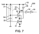
- FIG. 7 is a circuit diagram of a power-on reset circuit of a second embodiment of the invention.
- FIGS. 8A and 8B show waveforms for operating the power-on transistor shown in FIG. 7;
- FIG. 9 is a circuit diagram of a power-on reset circuit of the modified second embodiment of the invention.
- a power-on reset circuit 100 of the first embodiment includes a first NMOS transistor 11 , a second NMOS transistor 12 , a resistor 13 , a first inverter 14 , a second inverter 15 and a capacitor 16 .
- the power-on reset circuit 100 receives a power supply voltage Vdd from a power supply via a power supply line 10 .
- a gate of the first NMOS transistor 11 and a gate of the second NMOS transistor 12 are commonly connected to the line 10 .
- a silicon substrate or a well formed on the silicon substrate on which the first and second NMOS transistors 11 and 12 are formed (back gates of the NMOS transistors 11 and 12 ), is connected to ground.
- a source of the first NMOS transistor 11 is connected to ground.
- a drain of the first NMOS transistor 11 is connected to a source of the second NMOS transistor 12 through a node N 4 .
- a drain of the second NMOS transistor 12 is connected to one end of the resistor 13 through a node N 3 . The other end of the resistor 13 is connected to the power supply line 10 .
- An input terminal of the first inverter 14 is connected to the node N 3 .
- the input terminal of the second inverter 15 is connected to an output terminal of the first inverter 14 .
- the capacitor 16 is connected between the power supply line 10 and the node N 4 .
- FIG. 6A shows waveforms for operating the power-on transistor 100 when the power supply voltage going up rapidly
- FIG. 6B shows waveforms for operating the power-on transistor 100 when the power supply voltage going up gradually.
- the first NMOS transistor 11 and the second NMOS transistors 12 are off at an initial status which means that power is not supplied.
- the power supply voltage Vdd is applied to the power supply line 10 .
- the voltage applied to the gates of the first and second NMOS transistors 11 , 12 goes up in accordance with the increase of the power supply voltage Vdd.
- a threshold voltage Vti of the inverters 14 , 15 also goes up in proportion to the increase of the power supply voltage Vdd.
- the voltages at the node N 3 and the voltage at the node N 4 also go up similar to the power supply voltage Vdd. While the power supply voltage Vdd goes up, the capacitor 16 is charged. Further, the first inverter 14 outputs a L level signal having ground level and the second inverter outputs an H level signal having the power supply voltage level Vdd.
- the power supply voltage Vdd reaches to a threshold voltage Vtn of the NMOS transistors 11 and 12 .
- the first and second NMOS transistors 11 , 12 turn on.
- An electric current flows from the charged capacitor 16 to ground through the first NMOS transistor 11 , so that the voltage level at the node N 4 falls.
- the voltage of the node N 3 still goes up similar to the power supply voltage Vdd.
- the electric charge in the capacitor 16 runs out and the electric current flows from the power supply line 10 to ground through the resistor 13 and the first and second NMOS transistors 11 and 12 .
- the capacitor 16 delays the drop of the voltage at the node N 3 .
- the voltage at the node N 3 goes down to the threshold voltage Vti of the first inverter 14 , the output signal of the first inverter 14 turns from the L level to the H level. Therefore, the output signal of the second inverter 15 turns from the H level to the L level.
- the second inverter 15 outputs a signal as a reset pulse signal P. Then, the reset pulse signal having a few nanoseconds pulse width is applied from the output of the second inverter 15 to an internal circuit of the semiconductor device.
- the power supply voltage Vdd reaches to a threshold voltage Vtn of the NMOS transistors 11 and 12 .
- the first and second NMOS transistors 11 , 12 turn on.
- An electric current flows from the charged capacitor 16 to ground through the first NMOS transistor 11 , so that the voltage level at the node N 4 falls.
- the voltage of the node N 3 still goes up similar to the power supply voltage Vdd.
- the electric charge in the capacitor 16 runs out and the electric current flows from the power supply line 10 to ground through the resistor 13 and the first and second NMOS transistors 11 and 12 .
- the capacitor 16 delays the drop of the voltage at the node N 3 .
- the voltage at the node N 3 goes down to the threshold voltage Vti of the first inverter 14 , the output signal of the first inverter 14 turns from the L level to the H level which is still going up to similar to the power supply voltage Vdd.
- the output signal of the second inverter 15 turns from the H level to the L level.
- the second inverter 15 outputs a signal as a reset pulse signal P to an internal circuit of the semiconductor device.
- the first and second NMOS transistors 11 , 12 are connected in series between ground and the resistor 12 which is connected to the power supply line 10 .
- the capacitor 16 is connected between the power supply line 10 and the node N 4 which is located between the NMOS transistors 11 , 12 . Therefore, the change of the voltage at the node N 3 is delayed after the power supply voltage Vdd exceeds the threshold voltage Vtn of the first and second NMOS transistors 11 and 12 . That is, a reset pulse signal is generated certainly, even if the power supply voltage Vdd goes up rapidly.
- the capacitor 16 works as a delay circuit for delaying the fall of the voltage at the node N 3 . Therefore, it is not necessary to add delay circuits between the NMOS transistors and the power supply, so that it is easy to design and manufacture a power-on reset circuit.
- a power-on reset circuit 200 of the second embodiment includes a delay circuit 20 in addition to the circuit 100 shown in FIG. 1 . That is, the power-on reset circuit 200 includes the delay circuit 20 , a first NMOS transistor 31 , a second NMOS transistor 32 , a first resistor 33 , a first inverter 34 , a second inverter 35 and a first capacitor 36 .
- the delay circuit 20 which is connected between a power supply line 10 and ground, includes a second resistor 21 having 1 k ⁇ and a second capacitor 22 connected in series through a node N 5 .
- a silicon substrate or a well formed on the silicon substrate on which the first and second NMOS transistors 31 and 32 are formed (back gates of the NMOS transistors 31 and 32 ) is connected to ground.
- a source of the first NMOS transistor 31 is connected to ground.
- a drain of the first NMOS transistor 31 is connected to a source of the second NMOS transistor 32 through a node N 7 .
- a drain of the second NMOS transistor 32 is connected to one end of the first resistor 33 through a node N 6 .
- the other end of the first resistor 33 is connected to the power supply line 10 .
- the resistance value of the first resistor 33 is set to 4 M ⁇ .
- An input terminal of the fist inverter 34 is connected to the node N 6 .
- the input terminal of the second inverter 35 is connected to an output terminal of the first inverter 34 .
- the capacitor 36 is connected between the power supply line 10 and the node N 7 .
- a gate of the first NMOS transistor 31 is connected to the power supply line 10 .
- a gate of the second NMOS transistor 32 is connected to the node N 5 .
- the second resistor 21 is connected between the power supply line 10 and the node N 5 .
- the second capacitor 22 is connected between the node N 5 and ground.
- the first and second NMOS transistors 31 and 32 are in off-status before the power supply voltage Vdd is applied to the line 10 .
- the power supply voltage Vdd applied to the line 10 goes up.
- the voltage applied to the gate of the first NMOS transistor 31 goes up because the gate of the first NMOS transistor 31 is directly connected to the line 10 .
- the power supply voltage Vdd is applied to the gate of the second NMOS transistor 32 with a certain time delay from the application of the power supply voltage Vdd to the first NMOS transistor 31 because the gate of the second NMOS transistor 32 is connected to the line 10 through delay circuit 20 .
- the threshold voltage Vti of the inverters 34 and 35 goes up in proportion to the increase of the power supply voltage Vdd. While the power supply voltage Vdd goes up, the capacitor 36 is charged. Further, the first inverter 31 outputs the L level signal having ground level, and the second inverter 32 outputs the H level signal having the power supply level Vdd.
- the power supply voltage Vdd reaches the threshold voltage Vtn of the first NMOS transistor 31 , and the first NMOS transistor 31 is turned on.
- the voltage at the node N 6 goes down to the threshold voltage Vti of the first inverter 34 , the output signal of the first inverter 34 turns from the L level to the H level. Therefore, the output signal of the second inverter 35 turns from the H level to the L level.
- the second inverter 35 outputs a signal as a reset pulse signal P. Then the reset pulse signal P having a few nanoseconds pulse width is applied from the output of the second inverter 35 to an internal circuit of the semiconductor device.
- the power supply voltage Vdd reaches a threshold voltage Vtn of the first NMOS transistors 31 .
- the first NMOS transistor 31 turns on.
- An electric current flows from the charged capacitor 36 to ground through the first NMOS transistor 31 , so that the voltage level at the node N 7 falls.
- the second NMOS transistor 32 still be in the off state, the voltage of the node N 6 goes up similar to the power supply voltage Vdd.
- the second NMOS transistor 32 turns on. Then, the current flows from the power supply line 10 to ground through the first resistor 33 , the node N 6 , the first NMOS transistor 31 and the second NMOS transistor 32 .
- the delay circuit 20 delays the drop in the voltage at the node N 6 .
- the voltage at the node N 6 goes down to the threshold voltage Vti of the first inverter 34 , and the output signal of the first inverter 34 turns from the L level to the H level. Therefore, the output signal of the second inverter 35 turns from the H level to the L level. Since the resistance value of the first resistor 33 is higher than that of the second resistor 21 , a drain current of the second NMOS transistor 32 is restricted. The power supply voltage Vdd is applied to the gate of the second NMOS transistor 32 with the certain delay determined by the delay circuit 20 , a switching operation of the second NMOS transistor 32 is slow.
- the power-on circuit 200 has a high reliability for a variation of the voltage of the power supply.
- the one end of the capacitor 16 or 36 may be connected to ground instead of the power supply line 10 .
- the capacitor 16 or 36 By connecting the capacitor 16 or 36 to ground, the current flowing through the first NMOS transistor 11 or 31 can be delayed.
- the output of the delay circuit 20 may be connected to the gate of the first NMOS transistor 31 instead of the gate of the second NMOS transistor 32 as shown in FIG. 9 . Further, the output of the delay circuit may be connected to both of the gates of the first and second NMOS transistor 31 and 32 . As to the capacitor 36 , it may be omitted from the power-on reset circuit 200 .
- the NMOS transistors should be replaced to PMOS transistor when the power supply voltage is lower than ground voltage.
Abstract
Description
Claims (12)
Applications Claiming Priority (2)
| Application Number | Priority Date | Filing Date | Title |
|---|---|---|---|
| JP12313199 | 1999-04-28 | ||
| JP11-123131 | 1999-04-28 |
Publications (1)
| Publication Number | Publication Date |
|---|---|
| US6335646B1 true US6335646B1 (en) | 2002-01-01 |
Family
ID=14852960
Family Applications (1)
| Application Number | Title | Priority Date | Filing Date |
|---|---|---|---|
| US09/552,315 Expired - Fee Related US6335646B1 (en) | 1999-04-28 | 2000-04-19 | Power-on reset circuit for generating a reset pulse signal upon detection of a power supply voltage |
Country Status (1)
| Country | Link |
|---|---|
| US (1) | US6335646B1 (en) |
Cited By (12)
| Publication number | Priority date | Publication date | Assignee | Title |
|---|---|---|---|---|
| US20030019550A1 (en) * | 2000-09-01 | 2003-01-30 | Hlady Craig O. | Medium carbon steel sheet and strip having enhanced uniform elongation and method for production thereof |
| US6556058B2 (en) * | 2000-03-29 | 2003-04-29 | Mitsubishi Denki Kabushiki Kaisha | Power on reset circuit |
| US6650154B2 (en) * | 2001-11-28 | 2003-11-18 | Fujitsu Limited | Starter circuit |
| US20040169974A1 (en) * | 2002-02-28 | 2004-09-02 | Minoru Okamoto | Semiconductor integrated circuit and its reset method |
| US20050104571A1 (en) * | 2003-11-13 | 2005-05-19 | Hynix Semiconductor Inc. | Power-up signal generating circuit |
| US20050104635A1 (en) * | 2003-11-14 | 2005-05-19 | Oki Electric Industry Co., Ltd. | Power-on reset circuit |
| US20060232324A1 (en) * | 2005-04-15 | 2006-10-19 | Yong-Zhao Huang | Control circuit for command signals of clock generator |
| US20080030257A1 (en) * | 2006-08-04 | 2008-02-07 | Infineon Technologies Austria Ag | Driver Circuit for a Semiconductor Power Switching Element |
| CN101622704A (en) * | 2008-02-06 | 2010-01-06 | 松下电器产业株式会社 | Semiconductor device and method for resetting the same |
| US20130194011A1 (en) * | 2012-01-30 | 2013-08-01 | Seiko Instruments Inc. | Power-on reset circuit |
| US8547147B2 (en) | 2011-04-28 | 2013-10-01 | Fairchild Semiconductor Corporation | Power-on-reset circuit and reset method |
| TWI509398B (en) * | 2012-10-24 | 2015-11-21 | Htc Corp | Electronic apparatus and method for determining a reset thereof |
Citations (10)
| Publication number | Priority date | Publication date | Assignee | Title |
|---|---|---|---|---|
| JPS5880928A (en) | 1981-11-09 | 1983-05-16 | Sharp Corp | Automatic generating circuit for reset trigger in supplying power |
| US4551841A (en) * | 1982-06-09 | 1985-11-05 | Fujitsu Limited | One-chip semiconductor device incorporating a power-supply-potential detecting circuit with reset function |
| US4581552A (en) * | 1984-02-17 | 1986-04-08 | Texas Instruments Incorporated | Power-up clear circuitry having two thresholds |
| US4812679A (en) * | 1987-11-09 | 1989-03-14 | Motorola, Inc. | Power-on reset circuit |
| US4970408A (en) * | 1989-10-30 | 1990-11-13 | Motorola, Inc. | CMOS power-on reset circuit |
| US4985641A (en) * | 1988-05-07 | 1991-01-15 | Mitsubishi Denki Kabushiki Kaisha | Semiconductor integrated circuit device having selectable operational functions |
| US5180926A (en) * | 1991-11-26 | 1993-01-19 | Sequoia Semiconductor, Inc. | Power-on reset architecture |
| US5847586A (en) * | 1995-11-08 | 1998-12-08 | Burstein; Steven | Enhanced power-on-reset/low voltage detection circuit |
| US6121803A (en) * | 1998-06-26 | 2000-09-19 | Oki Electric Industry Co., Ltd. | Pulse generator |
| US6204701B1 (en) * | 1994-05-31 | 2001-03-20 | Texas Instruments Incorporated | Power up detection circuit |
-
2000
- 2000-04-19 US US09/552,315 patent/US6335646B1/en not_active Expired - Fee Related
Patent Citations (10)
| Publication number | Priority date | Publication date | Assignee | Title |
|---|---|---|---|---|
| JPS5880928A (en) | 1981-11-09 | 1983-05-16 | Sharp Corp | Automatic generating circuit for reset trigger in supplying power |
| US4551841A (en) * | 1982-06-09 | 1985-11-05 | Fujitsu Limited | One-chip semiconductor device incorporating a power-supply-potential detecting circuit with reset function |
| US4581552A (en) * | 1984-02-17 | 1986-04-08 | Texas Instruments Incorporated | Power-up clear circuitry having two thresholds |
| US4812679A (en) * | 1987-11-09 | 1989-03-14 | Motorola, Inc. | Power-on reset circuit |
| US4985641A (en) * | 1988-05-07 | 1991-01-15 | Mitsubishi Denki Kabushiki Kaisha | Semiconductor integrated circuit device having selectable operational functions |
| US4970408A (en) * | 1989-10-30 | 1990-11-13 | Motorola, Inc. | CMOS power-on reset circuit |
| US5180926A (en) * | 1991-11-26 | 1993-01-19 | Sequoia Semiconductor, Inc. | Power-on reset architecture |
| US6204701B1 (en) * | 1994-05-31 | 2001-03-20 | Texas Instruments Incorporated | Power up detection circuit |
| US5847586A (en) * | 1995-11-08 | 1998-12-08 | Burstein; Steven | Enhanced power-on-reset/low voltage detection circuit |
| US6121803A (en) * | 1998-06-26 | 2000-09-19 | Oki Electric Industry Co., Ltd. | Pulse generator |
Cited By (19)
| Publication number | Priority date | Publication date | Assignee | Title |
|---|---|---|---|---|
| US6556058B2 (en) * | 2000-03-29 | 2003-04-29 | Mitsubishi Denki Kabushiki Kaisha | Power on reset circuit |
| US6710634B2 (en) | 2000-03-29 | 2004-03-23 | Renesas Technology Corp. | Power on reset circuit |
| US20030019550A1 (en) * | 2000-09-01 | 2003-01-30 | Hlady Craig O. | Medium carbon steel sheet and strip having enhanced uniform elongation and method for production thereof |
| US6650154B2 (en) * | 2001-11-28 | 2003-11-18 | Fujitsu Limited | Starter circuit |
| US20040169974A1 (en) * | 2002-02-28 | 2004-09-02 | Minoru Okamoto | Semiconductor integrated circuit and its reset method |
| US6879193B2 (en) * | 2002-02-28 | 2005-04-12 | Matsushita Electric Industrial Co., Ltd. | Semiconductor integrated circuit and its reset method |
| US20050104571A1 (en) * | 2003-11-13 | 2005-05-19 | Hynix Semiconductor Inc. | Power-up signal generating circuit |
| US6982577B2 (en) * | 2003-11-14 | 2006-01-03 | Oki Electric Industry, Co., Ltd. | Power-on reset circuit |
| US20050104635A1 (en) * | 2003-11-14 | 2005-05-19 | Oki Electric Industry Co., Ltd. | Power-on reset circuit |
| US20060232324A1 (en) * | 2005-04-15 | 2006-10-19 | Yong-Zhao Huang | Control circuit for command signals of clock generator |
| US7298186B2 (en) * | 2005-04-15 | 2007-11-20 | Hong Fu Jin Precision Industry (Shen Zhen) Co., Ltd. | Control circuit for command signals of clock generator |
| US20080030257A1 (en) * | 2006-08-04 | 2008-02-07 | Infineon Technologies Austria Ag | Driver Circuit for a Semiconductor Power Switching Element |
| US7642817B2 (en) * | 2006-08-04 | 2010-01-05 | Infineon Technologies Austria Ag | Driver circuit for a semiconductor power switching element |
| CN101622704A (en) * | 2008-02-06 | 2010-01-06 | 松下电器产业株式会社 | Semiconductor device and method for resetting the same |
| US20100327915A1 (en) * | 2008-02-06 | 2010-12-30 | Tsuyoshi Imanaka | Semiconductor device and method for resetting the same |
| US8547147B2 (en) | 2011-04-28 | 2013-10-01 | Fairchild Semiconductor Corporation | Power-on-reset circuit and reset method |
| US20130194011A1 (en) * | 2012-01-30 | 2013-08-01 | Seiko Instruments Inc. | Power-on reset circuit |
| US8797070B2 (en) * | 2012-01-30 | 2014-08-05 | Seiko Instruments Inc. | Power-on reset circuit |
| TWI509398B (en) * | 2012-10-24 | 2015-11-21 | Htc Corp | Electronic apparatus and method for determining a reset thereof |
Similar Documents
| Publication | Publication Date | Title |
|---|---|---|
| US6914461B2 (en) | Power-on reset circuits including first and second signal generators and related methods | |
| US5469099A (en) | Power-on reset signal generator and operating method thereof | |
| JP3756961B2 (en) | Chip initialization signal generation circuit for semiconductor memory device | |
| US6104221A (en) | Power-up detection circuit of a semiconductor device | |
| US6335646B1 (en) | Power-on reset circuit for generating a reset pulse signal upon detection of a power supply voltage | |
| US6411554B1 (en) | High voltage switch circuit having transistors and semiconductor memory device provided with the same | |
| US20050140404A1 (en) | Power-up circuit in semiconductor memory device | |
| US20060028253A1 (en) | Power-on reset circuit | |
| KR100440448B1 (en) | Semiconductor integrated circuit device capable of securing time delay insensitive to temperature variation | |
| US7482847B2 (en) | Power-on reset circuit | |
| US5930129A (en) | Power on reset circuit | |
| US7046054B2 (en) | Power up signal generator | |
| US6958641B2 (en) | Delay circuit with more-responsively adapting delay time | |
| US7098713B2 (en) | Delay circuit having function of filter circuit | |
| US11777481B2 (en) | Noise-tolerant delay circuit | |
| JP2000021179A (en) | Boosting circuit and semiconductor device using the same | |
| US6121803A (en) | Pulse generator | |
| US20050093610A1 (en) | Delay circuit with constant delay time regardless of process condition or voltage variation and pulse generator using the same | |
| KR100630977B1 (en) | Power on reset circuit | |
| KR100239884B1 (en) | Voltage level shift circuit | |
| KR100715601B1 (en) | Power-on reset circuit | |
| JP2005039635A (en) | Power-on reset circuit | |
| KR0132369B1 (en) | Data input buffer for semiconductor integrated device and buffering method thereof | |
| JP3474148B2 (en) | Power-on reset circuit | |
| KR100215761B1 (en) | Level shift circuit in semiconductor memory device |
Legal Events
| Date | Code | Title | Description |
|---|---|---|---|
| AS | Assignment |
Owner name: OKI ELECTRIC INDUSTRY CO., LTD., JAPAN Free format text: ASSIGNMENT OF ASSIGNORS INTEREST;ASSIGNOR:NAGATOMO, SHIGERU;REEL/FRAME:010743/0538 Effective date: 20000404 |
|
| FPAY | Fee payment |
Year of fee payment: 4 |
|
| AS | Assignment |
Owner name: OKI SEMICONDUCTOR CO., LTD., JAPAN Free format text: CHANGE OF NAME;ASSIGNOR:OKI ELECTRIC INDUSTRY CO., LTD.;REEL/FRAME:022399/0969 Effective date: 20081001 Owner name: OKI SEMICONDUCTOR CO., LTD.,JAPAN Free format text: CHANGE OF NAME;ASSIGNOR:OKI ELECTRIC INDUSTRY CO., LTD.;REEL/FRAME:022399/0969 Effective date: 20081001 |
|
| FPAY | Fee payment |
Year of fee payment: 8 |
|
| REMI | Maintenance fee reminder mailed | ||
| LAPS | Lapse for failure to pay maintenance fees | ||
| STCH | Information on status: patent discontinuation |
Free format text: PATENT EXPIRED DUE TO NONPAYMENT OF MAINTENANCE FEES UNDER 37 CFR 1.362 |
|
| FP | Lapsed due to failure to pay maintenance fee |
Effective date: 20140101 |