US6263735B1 - Acceleration sensor - Google Patents
Acceleration sensor Download PDFInfo
- Publication number
- US6263735B1 US6263735B1 US09/284,960 US28496099A US6263735B1 US 6263735 B1 US6263735 B1 US 6263735B1 US 28496099 A US28496099 A US 28496099A US 6263735 B1 US6263735 B1 US 6263735B1
- Authority
- US
- United States
- Prior art keywords
- cap
- mass substance
- sensor
- acceleration sensor
- sensor section
- Prior art date
- Legal status (The legal status is an assumption and is not a legal conclusion. Google has not performed a legal analysis and makes no representation as to the accuracy of the status listed.)
- Expired - Fee Related
Links
Images


Classifications
-
- G—PHYSICS
- G01—MEASURING; TESTING
- G01P—MEASURING LINEAR OR ANGULAR SPEED, ACCELERATION, DECELERATION, OR SHOCK; INDICATING PRESENCE, ABSENCE, OR DIRECTION, OF MOVEMENT
- G01P15/00—Measuring acceleration; Measuring deceleration; Measuring shock, i.e. sudden change of acceleration
- G01P15/02—Measuring acceleration; Measuring deceleration; Measuring shock, i.e. sudden change of acceleration by making use of inertia forces using solid seismic masses
- G01P15/08—Measuring acceleration; Measuring deceleration; Measuring shock, i.e. sudden change of acceleration by making use of inertia forces using solid seismic masses with conversion into electric or magnetic values
- G01P15/125—Measuring acceleration; Measuring deceleration; Measuring shock, i.e. sudden change of acceleration by making use of inertia forces using solid seismic masses with conversion into electric or magnetic values by capacitive pick-up
-
- G—PHYSICS
- G01—MEASURING; TESTING
- G01P—MEASURING LINEAR OR ANGULAR SPEED, ACCELERATION, DECELERATION, OR SHOCK; INDICATING PRESENCE, ABSENCE, OR DIRECTION, OF MOVEMENT
- G01P15/00—Measuring acceleration; Measuring deceleration; Measuring shock, i.e. sudden change of acceleration
- G01P15/02—Measuring acceleration; Measuring deceleration; Measuring shock, i.e. sudden change of acceleration by making use of inertia forces using solid seismic masses
- G01P15/08—Measuring acceleration; Measuring deceleration; Measuring shock, i.e. sudden change of acceleration by making use of inertia forces using solid seismic masses with conversion into electric or magnetic values
- G01P15/0802—Details
-
- G—PHYSICS
- G01—MEASURING; TESTING
- G01P—MEASURING LINEAR OR ANGULAR SPEED, ACCELERATION, DECELERATION, OR SHOCK; INDICATING PRESENCE, ABSENCE, OR DIRECTION, OF MOVEMENT
- G01P15/00—Measuring acceleration; Measuring deceleration; Measuring shock, i.e. sudden change of acceleration
- G01P15/02—Measuring acceleration; Measuring deceleration; Measuring shock, i.e. sudden change of acceleration by making use of inertia forces using solid seismic masses
- G01P15/08—Measuring acceleration; Measuring deceleration; Measuring shock, i.e. sudden change of acceleration by making use of inertia forces using solid seismic masses with conversion into electric or magnetic values
- G01P15/09—Measuring acceleration; Measuring deceleration; Measuring shock, i.e. sudden change of acceleration by making use of inertia forces using solid seismic masses with conversion into electric or magnetic values by piezoelectric pick-up
- G01P15/0922—Measuring acceleration; Measuring deceleration; Measuring shock, i.e. sudden change of acceleration by making use of inertia forces using solid seismic masses with conversion into electric or magnetic values by piezoelectric pick-up of the bending or flexing mode type
-
- G—PHYSICS
- G01—MEASURING; TESTING
- G01P—MEASURING LINEAR OR ANGULAR SPEED, ACCELERATION, DECELERATION, OR SHOCK; INDICATING PRESENCE, ABSENCE, OR DIRECTION, OF MOVEMENT
- G01P15/00—Measuring acceleration; Measuring deceleration; Measuring shock, i.e. sudden change of acceleration
- G01P15/02—Measuring acceleration; Measuring deceleration; Measuring shock, i.e. sudden change of acceleration by making use of inertia forces using solid seismic masses
- G01P15/08—Measuring acceleration; Measuring deceleration; Measuring shock, i.e. sudden change of acceleration by making use of inertia forces using solid seismic masses with conversion into electric or magnetic values
- G01P15/12—Measuring acceleration; Measuring deceleration; Measuring shock, i.e. sudden change of acceleration by making use of inertia forces using solid seismic masses with conversion into electric or magnetic values by alteration of electrical resistance
- G01P15/123—Measuring acceleration; Measuring deceleration; Measuring shock, i.e. sudden change of acceleration by making use of inertia forces using solid seismic masses with conversion into electric or magnetic values by alteration of electrical resistance by piezo-resistive elements, e.g. semiconductor strain gauges
-
- G—PHYSICS
- G01—MEASURING; TESTING
- G01P—MEASURING LINEAR OR ANGULAR SPEED, ACCELERATION, DECELERATION, OR SHOCK; INDICATING PRESENCE, ABSENCE, OR DIRECTION, OF MOVEMENT
- G01P15/00—Measuring acceleration; Measuring deceleration; Measuring shock, i.e. sudden change of acceleration
- G01P15/02—Measuring acceleration; Measuring deceleration; Measuring shock, i.e. sudden change of acceleration by making use of inertia forces using solid seismic masses
- G01P15/08—Measuring acceleration; Measuring deceleration; Measuring shock, i.e. sudden change of acceleration by making use of inertia forces using solid seismic masses with conversion into electric or magnetic values
- G01P2015/0805—Measuring acceleration; Measuring deceleration; Measuring shock, i.e. sudden change of acceleration by making use of inertia forces using solid seismic masses with conversion into electric or magnetic values being provided with a particular type of spring-mass-system for defining the displacement of a seismic mass due to an external acceleration
- G01P2015/0822—Measuring acceleration; Measuring deceleration; Measuring shock, i.e. sudden change of acceleration by making use of inertia forces using solid seismic masses with conversion into electric or magnetic values being provided with a particular type of spring-mass-system for defining the displacement of a seismic mass due to an external acceleration for defining out-of-plane movement of the mass
- G01P2015/0825—Measuring acceleration; Measuring deceleration; Measuring shock, i.e. sudden change of acceleration by making use of inertia forces using solid seismic masses with conversion into electric or magnetic values being provided with a particular type of spring-mass-system for defining the displacement of a seismic mass due to an external acceleration for defining out-of-plane movement of the mass for one single degree of freedom of movement of the mass
- G01P2015/0828—Measuring acceleration; Measuring deceleration; Measuring shock, i.e. sudden change of acceleration by making use of inertia forces using solid seismic masses with conversion into electric or magnetic values being provided with a particular type of spring-mass-system for defining the displacement of a seismic mass due to an external acceleration for defining out-of-plane movement of the mass for one single degree of freedom of movement of the mass the mass being of the paddle type being suspended at one of its longitudinal ends
Definitions
- the present invention relates to an acceleration sensor for use in the control of a vehicle body and the like application fields.
- the invention also includes the producing method.
- a high precision acceleration sensor is presented at a low cost, without using high-level semiconductor technologies or micro-machining technologies.
- Means for detecting the strain includes the one which makes use of the change in the electrostatic capacitance, and the one which makes use of the piezoresistance effect, for example.
- Acceleration sensors using a single crystal silicon for the sensing portion have a stable performance and are capable of measuring the acceleration at high precision level. Therefore, the sensors of the above category form the mainstream in the recent field of acceleration sensors.
- Japanese Laid-open Patent No.05-340957 discloses a method of joining an auxiliary glass substrate to a silicon substrate forming the hinge portion by anode bonding.
- the anode bonding method requires a facility for providing electric fields among the bonding substrates.
- the anode bonding is available only with a glass that contains sodium. The anode bonding method is not simple to practice, and restrictive in selecting the glass material.
- acceleration sensor uses a piezoelectric element for the portion at which a strain is caused by acceleration.
- a static acceleration such as the measurement of an inclination relative to the gravity of the earth.
- an acceleration sensor is required to have a self-diagnostic function. Most of such self-diagnostic functions require to have complicated peripheral circuits.
- the present invention addresses the above described drawbacks, and aims to offer an inexpensive, yet highly accurate, acceleration sensor formed of silicon and other materials, without asking for the help of the high level semiconductor technologies or the micro-machining technologies.
- the acceleration sensor in accordance with the present invention covers a wide range of the frequency in acceleration measurement, and is capable of making a self-diagnosis about a disorder.
- the present invention also offers a method for manufacturing such acceleration sensors.
- the hinge portion of a sensor section which portion is strained by an acceleration force, is formed of silicon; while the auxiliary portions, a cover and a mass substance for receiving the acceleration are structured of glass or other materials.
- Joining of the different materials is conducted by direct bonding.
- the direct bonding is a technology that joins different kinds of materials by simply making the bonding surfaces ultra-clean.
- the direct bonding technology assures a firm joining between the materials themselves, by making the bonding surfaces clean and heating the surfaces at a high temperature in the atmospheric environment or in the vacuum; without intervening any foreign material, such as an adhesive substance, or providing any electric fields which were essential in the anode bonding.
- the direct bonding produces a rigid joining at an inexpensive cost.
- the direct bonding can join silicon, glass, non-alkaline glass, quartz glass and various monocrystalline substrates together.
- the hinge portion of said silicon substrate has to be processed to as thin as 10-30 ⁇ m thick.
- Joining a glass substrate to one surface of the silicon substrate by direct bonding and then grinding only the surface of silicon substrate may provide such a thin silicon substrate.
- a substrate can be ground down to approximately 10 ⁇ m at an accuracy level within ⁇ 1 ⁇ m. The accuracy level is high enough for processing the acceleration sensor of the present invention.
- an acceleration sensor By further providing a piezoelectric element, or a piezoresistive element, formed on the hinge portion, and attaching a glass case having an electrode for electrostatic capacitance in the corresponding area together, an acceleration sensor will have both of the features of electrostatic capacitance type and piezoelectric element type, or piezoresistive element type.
- acceleration sensors that can measure the acceleration for a wide range of frequency, capable of making the self-diagnosis can be manufactured efficiently with a high production yield rate.
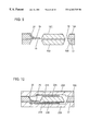
- FIG. 1 is an exploded perspective view showing a capacitance type acceleration sensor in accordance with a first exemplary embodiment of the present invention.
- FIG. 2 ( a ) is a cross sectional view of the capacitance type acceleration sensor.
- FIG. 2 ( b ) is a cross sectional view of a conventional capacitance type acceleration sensor.
- FIG. 3 shows cross sectional views used to describe the manufacturing process steps of the capacitance type acceleration sensor of embodiment 1.
- FIG. 4 shows cross sectional views used to describe other manufacturing process steps of the capacitance type acceleration sensor of embodiment 1.
- FIG. 5 shows cross sectional views used to describe process steps of manufacturing a case of the acceleration sensor of embodiment 1.
- FIG. 6 shows a cross sectional view used to describe a sensor section of the acceleration sensor of embodiment 1.
- FIG. 7 is a cross sectional view of the finished acceleration sensor of embodiment 1.
- FIG. 8 is a cross sectional view of the acceleration sensor of embodiment 1, in which the mass substance is provided only on one surface.
- FIG. 9 is a cross sectional view showing a sensor section of a piezoresistive type acceleration sensor in accordance with a second exemplary embodiment of the present invention.
- FIG. 10 is a cross sectional view showing a sensor section of a complex type acceleration sensor in accordance with a third exemplary embodiment of the present invention.
- FIG. 11 is an exploded perspective view showing an acceleration sensor of a fourth exemplary embodiment of the present invention.
- FIG. 12 is a perspective view used to show the manufacturing process of the acceleration sensor of embodiment 4.
- FIG. 13 is a perspective view showing the acceleration sensor of embodiment 4.
- FIG. 14 shows cross sectional views used to describe manufacturing process steps of the acceleration sensor of embodiment 4.
- FIG. 15 is an exploded perspective view showing an acceleration sensor in accordance with a fifth exemplary embodiment of the present invention.
- FIG. 16 is an exploded perspective view showing an acceleration sensor in accordance with a sixth exemplary embodiment of the present invention.
- FIG. 17 is a cross sectional view used to describe manufacturing process of an acceleration sensor in accordance with a seventh exemplary embodiment of the present invention.
- FIG. 18 shows cross sectional views used to describe method of forming resist patterns in embodiment 7.
- FIG. 19 shows a resist pattern on a wafer of embodiment 7.
- FIG. 20 is a cross sectional view used to describe manufacturing process of an acceleration sensor in accordance with an eighth exemplary embodiment of the present invention.
- FIG. 21 shows cross sectional views used to describe method of forming resist patterns in embodiment 8.
- FIG. 22 shows a pattern on a silicon substrate of an acceleration sensor in accordance with a ninth embodiment of the present invention, as viewed in a wafer state.
- FIG. 23 illustrates manufacturing process steps of an acceleration sensor in accordance with a tenth exemplary embodiment of the present invention.
- FIG. 1 is an exploded perspective view of a capacitance type acceleration sensor in accordance with a first exemplary embodiment of the present invention.
- a hollow area 9 A (not shown), 9 B is formed in a cap 8 A, 8 B for encapsulating a sensor section formed of the silicon substrate 1 and the auxiliary substrate 4 A, 4 B.
- a fixed electrode 10 A (not shown), 10 B is formed on the surface of the hollow area in a place opposing to the movable electrode 7 A, 7 B (not shown), and a lead electrode 10 C (not shown), 10 D for the fixed electrode is formed at a place in the opposite end relative to the lead electrode 7 C, 7 D (not shown) for the movable electrode.
- FIG. 2 ( a ) is a cross sectional view of the capacitance type acceleration sensor.
- the silicon substrate 1 as thin as 10-30 ⁇ m thick can move in the up/down (in the drawing) direction.
- the mass substance 6 A, 6 B moves up/down, and the movable electrode 7 A, 7 B moves accordingly.
- the electrostatic capacitance formed between the movable electrode 7 A and the fixed electrode 10 A, and that formed between the movable electrode 7 B and the fixed electrode 10 B change.
- the acceleration given to is detected in the form of a change in the electrostatic capacitance.
- FIG. 2 ( b ) a conventional capacitance type acceleration sensor is shown in FIG. 2 ( b ).
- a hinge portion 12 A and a mass substance 12 B for yielding a strain in response to an acceleration were formed as a one-piece silicon structure.
- a high-level process control is needed for thoroughly removing only the region corresponding to a groove 12 C, while keeping the region corresponding to the hinge portion 12 A left unremoved for the thickness 10-30 ⁇ m.
- the symbol 11 A, 11 B denotes a cap
- 13 A, 13 B is a fixed electrode
- 14 A, 14 B is a movable electrode.
- FIG. 3 ( a )-FIG. 3 ( e ) illustrate process steps for manufacturing a sensor section, which moves in response to acceleration.
- an auxiliary glass substrate 16 A and a silicon substrate 17 are joined together by direct bonding (FIG. 3 ( a )).
- the direct bonding technology does not require any adhesive or any foreign material, nor does it require any electric fields between the bonding materials which are the essential requirement in the anode bonding technology.
- the direct bonding provides a firm joining by simply, keeping the state of the surfaces of bonding materials at a high precision level and clean, and then heating these materials in the atmospheric environment or in the vacuum. It is an excellent bonding technology of low cost. Silicon, glass, non-alkaline glass, quartz glass and various monocrystalline substrates can be joined by direct bonding. Therefore, the present invention may be embodied in other forms using other materials.
- a preferred temperature and time of heating for the direct bonding between silicon and glass for example, are 300-500° C. for 1-2 hours.
- the surface of silicon substrate 17 is ground down to a certain specified thickness (FIG. 3 ( b )).
- a recent grinding technology assures the accuracy level within ⁇ 1 ⁇ m for the thickness of 10 ⁇ m. This means that the presently available grinding technique is enough for implementing the acceleration sensor.
- the surface of silicon substrate 17 is polished to a mirror surface in the final stage.
- an auxiliary glass substrate 16 B is joined on the surface of silicon substrate 17 by direct bonding (FIG. 3 ( c )).
- the auxiliary substrate 16 A, 16 B is etched to form the mass substance 16 C, 16 D (FIG. 3 ( d )). It is advantageous to select and use an appropriate etchant, with which the glass functions as the etching stopper.
- An etching mask (not shown) is provided so as to leave the silicon substrate 17 unetched only in a hinge portion 18 of a tongue shape. A slit 19 is thus formed by etching (FIG. 3 ( e )).
- the slit 19 may be formed by etching before the auxiliary substrate 16 B is joined by direct bonding, as shown in FIG. 4 .
- this procedure it is easy to apply an etching mask for etching the silicon substrate 17 , because the etching surface does not have any bump created by the auxiliary substrate 16 B.
- a case section is prepared as shown in FIG. 5 ( a ), ( b ).
- a hollow area 20 C, 20 D is provided in a glass cap 20 A, 20 B (FIG. 5 ( a )), and a fixed electrode 21 A, 21 B is formed on the bottom surface, as well as a lead electrode 21 C, 21 D for the fixed electrode (FIG. 5 ( b )).
- a movable electrode 23 A, 23 B and a lead electrode 23 C, 23 D for the movable electrode are formed also on the sensor section.
- the sensor section and the case section are joined by direct bonding to complete a capacitance type acceleration sensor, as shown in FIG. 7 .
- the electrodes may be lead outside also through the joint at a side face 26 B, instead of the side face 26 A only.
- Perforating a through hole in the case substrate may be another means of leading the electrode out. Any way, the electrode leading means is not limited to those described in the above.
- a glass plate has been used for the auxiliary substrate in the present embodiment 1, it is not intended to limit the material to the glass. Besides glass, a substrate of amorphous material such as quartz glass, or a monocrystalline substrate such as crystal may be used for the same effect. If there are certain specific requirements in the temperature characteristics of a material of the sensor, it is an advantage that in the present invention a most appropriate material can be selected among the group of materials.
- the auxiliary substrate has been provided at both surfaces of the silicon substrate in the present embodiment 1.
- the auxiliary substrate may be provided only at one surface of the silicon substrate if the symmetrical structure is not considered essential.
- a capacitance type acceleration sensor having the auxiliary substrate 16 A only at one surface, as shown in FIG. 8, may also be structured. Eliminating one bonding process for joining the auxiliary substrate contributes to simplify the total procedure.
- An acceleration sensor in accordance with a second embodiment of the present invention is that of embodiment 1, wherein, at the process step of FIG. 3 ( e ), a piezoresistive material, or a material which changes its electrical characteristics in accordance with strain, is formed in the region where a strain is caused by an acceleration.
- the piezoresistive material may be provided through a commonly used semiconductor technology, such as the sputtering, the ion implantation, etc.
- FIG. 9 shows the structure of a sensor section thus formed.
- the silicon substrate 17 is held supported by the auxiliary glass substrate 16 A, 16 B, and a piezoresistive element 25 and a lead electrode 24 are formed on the hinge portion 18 of a tongue shape.
- the piezoresistive element changes its resistance value in accordance with strain.
- the acceleration effected to the mass substance 16 C, 16 D can be measured by reading the change in the resistance value of the piezoresistive element 25 .
- the piezoresistive element 25 may be provided on any of the either surface. Encapsulating the sensor section with glass cap in the same way as in embodiment 1 completes a piezoresistive type acceleration sensor.
- auxiliary substrate In place of the glass used for the auxiliary substrate, materials other than the glass may be used, like in the case of embodiment 1.
- the auxiliary substrate may be provided only on one surface. The advantages of such configuration remain the same as in the embodiment 1.
- the piezoresistive element 25 may be replaced with a piezoelectric element.
- the piezoelectric element changes its resonance impedance, or resonance frequency, by a strain effected thereon.
- the acceleration effected to the sensor section can be measured by reading the value of the change.
- the piezoelectric element may be formed through a commonly used process, such as the sputtering.
- An acceleration sensor in accordance with a third exemplary embodiment of the present invention is a combination of the embodiment 1 and the embodiment 2.
- FIG. 10 shows a cross sectional view of the acceleration sensor of embodiment 3.
- the formation order for forming a piezoresistive element, or a piezoelectric element There is no limitation either as to whether the auxiliary substrate should be provided either one surface alone or on the both surfaces. What is to be done is to form a piezoresistive element 25 , or a piezoelectric element, and a lead electrode 24 before joining the upper and the lower caps of electrostatic capacitance type.
- an acceleration sensor may be provided simultaneously with the sensor functions of multiple types, the electrostatic capacitance type and the piezoresistive type, or the piezoelectric type.
- a static acceleration may be measured by the electrostatic capacitance type sensor, while a dynamic acceleration by the piezoelectric type sensor.
- FIG. 11 is an exploded perspective view showing a fourth exemplary embodiment of the present invention.
- a sensor section 30 comprises a mass substance 31 , a hinge portion 32 , and a frame 33 .
- a first fixed electrode 41 (not shown) and a second fixed electrode 51 are formed corresponding to a first movable electrode 35 a and a second movable electrode 35 b (not shown).
- the first and the second caps 40 , 50 are not provided with the hollow area, which existed in the embodiments 1-3. Instead, in the present embodiment 4, a space has been secured within the sensor section 30 for the mass substance 31 to make the up/down motion.
- An acceleration sensor may take either one of the structures, that of embodiments 1-3 or that of embodiment 4.
- a first lead electrode 36 a for the first movable electrode 35 a is formed in one of the four grooves ( 34 b in FIG. 11 ).
- a second movable electrode 35 b (not shown in FIG. 11) is provided, and its lead electrode (a second lead electrode 36 b , not shown) is taken to a location ( 34 c , for example) other than that of the first lead electrode 36 a.
- a second groove 44 a - 44 d is provided corresponding to the location of the first groove 34 a - 34 d in the frame 33 . Also on the sidewall of which groove 44 a - 44 c , an electrode film is formed.
- a first fixed electrode 41 (not shown) is formed on the reverse surface of the first cap 40 .
- a third lead electrode 46 (not shown) for the first fixed electrode 41 is taken to a place (a second groove 44 a , for example) other than that of first lead electrode 36 a and that of second lead electrode 36 b.
- an electrode film is provided in a place corresponding to the first groove 34 a - 34 d .
- a fourth lead electrode 56 for the second fixed electrode 5 l is provided in a place (on the electrode film of second cap 50 corresponding to first groove 34 d , for example) other than that of first lead electrode 36 a , that of second lead electrode 36 b and that of third lead electrode 46 .
- a method of manufacturing an acceleration sensor of the present embodiment 4 is described.
- a plurality of sensor sections 30 , a plurality of first caps 40 and a plurality of second caps 50 are formed, respectively, on a substrate 39 for the formation of sensor section, a substrate 49 for the formation of first cap and a substrate 59 for the formation of second cap.
- Each of the three substrates undergoes all the procedures as it is in the form of a wafer before they are bonded together to be separated into individual pieces.
- the acceleration sensors are manufactured efficiently maintaining a high accuracy level.
- An electrode film is formed on both surfaces of the substrate 39 for the formation of sensor section and the substrate 49 for the formation of first cap, and on one surface of the substrate 59 for the formation of second cap, by deposition of Cr/Au, Ti/Au or the like material in vacuum. Then, these substrates are joined together by direct bonding. After the bonding, an electroconductive paste is poured into the through holes from second through hole 44 a - 44 d , and hardened. The wafers bonded together to form a single piece is separated into individual pieces using a dicing saw or the like facility. A finished acceleration sensor manufactured through the above procedure is shown in FIG. 13 .
- a silicon substrate 37 having an insulating oxide film on the surface and a glass substrate (lower) 38 a are joined together by direct bonding.
- the silicon surface is ground to be a thin plate (FIG. 14 ( a )).
- the hinge portion 37 a and the groove (silicon substrate) 37 b are formed on the silicon substrate 37 (FIG. 14 ( b )).
- the wet etching process or the dry etching process may be used for the formation.
- Another glass substrate (upper) 38 b is direct bonded on the ground surface of the silicon substrate 37 (FIG. 14 ( c )). Then it undergoes the sand blasting process, or the wet etching process, so as only the frame portion 38 c and the mass substance 38 d remain unblasted on the glass substrate 38 a , 38 b (FIG. 14 ( d )). Simultaneously, a groove (glass substrate) 38 e is formed.
- a cut is provided by etching or the like method in the place where a lead electrode is formed. This is aimed to prevent the lead electrode from intervening in the space of direct bonding between the substrates.
- the use of the sand blasting process, or the wet etching process, for the formation of the glass substrate (FIG. 14 ( d )) produces a bowl shaped taper in the cross section of the glass substrate. The tapered shape is advantageous in forming and connecting the electrodes on the upper and the lower surfaces.
- a similar advantage is provided by the use of the sand blasting process, or the wet etching process, for perforating the second through hole in the first cap.
- each of the lead electrodes are locating on one surface, and the electrode for output has a relatively large size, as illustrated in FIG. 13 . This is an advantageous factor for increasing the efficiency in the wire bonding and other operations.
- the above described method of forming a sensor section is an example. Alternative methods may be considered by changing the sequence of process steps, or the sensor section may be formed by using the methods as described in the above embodiments 1-3. Or, an equivalent shape may be formed on a piece substrate of silicon through a fine pattern technology using etching process. In this case, use of an anisotropic wet etching process is effective.
- the shape of one-end support has been described in the foregoing, it can also take a shape of both-end support, or it can be supported by a plurality of supports for producing the same effect.
- An acceleration sensor in accordance with a fifth exemplary embodiment of the present invention is the one having a structure similar to that of the embodiment 2, wherein a piezoresistive element or a piezoelectric element is used in the sensor section. Substantially, there is no significant difference as compared with the acceleration sensor of embodiment 4.
- Numeral 70 denotes the piezoresistive element, the piezoelectric element, in FIG. 15 . As all of the electrodes are located concentrated on one plane, there is no need for a lead electrode going down to the second cap 50 . The lead electrode is needed only for the connection in the level of sensor section 30 and higher.
- An acceleration sensor in accordance with a sixth exemplary embodiment of the present invention relates to an acceleration sensor of a higher precision level.
- the sensor section of which acceleration sensor, having a similar structure as that of the embodiment 3, comprises a combination of an electrostatic capacitance type structure and a piezoresistive element, or a piezoelectric element. Basically, there is no substantial difference as compared with the embodiment 4. By simply increasing the number of the through holes, similar effects as those of the embodiment 4 are produced. As illustrated in FIG.
- additional grooves ( 34 e - 34 h , 44 e - 44 h ) are provided in the respective four sides, besides the grooves ( 34 a - 34 d , 44 a - 44 d ) of embodiment 4 provided at the four corners of the device.
- the relevant lead electrodes are formed in an arrangement where the connection becomes the shortest.
- the number of process steps regarding the lead electrode does not increase in the present embodiment 6. So the added functions do not invite an increased manufacturing cost in this respect.
- FIG. 17 is a cross sectional view used to describe a seventh exemplary embodiment of the present invention.
- FIG. 18 shows cross sectional views used to describe the formation of respective resist patterns in embodiment 7.
- FIG. 19 is the resist pattern as seen on a wafer.
- FIG. 17 a glass substrate 71 , a silicon substrate 72 , a wet etching resist 73 , and a sand blasting resist 74 are shown.
- FIG. 19 a mass substance 71 a , an auxiliary substrate 71 b , a wet etching resist pattern 73 a and a sand blasting resist pattern 74 a are shown.
- FIG. 18 shows an appearance of the resist patterns formed on a wafer as viewed from the surface of glass substrate. As shown in FIG. 17, the wafer is sandblasted up to just before penetration of the glass substrate 71 (numeral 76 a represents the processing line by the sand blasting). The wafer in this stage is immersed in an etchant, liquid containing ammonium bifluoide, to have the glass substrate 71 penetrated through (numeral 76 b represents the processing line by the wet etching).
- Penetrating a glass plate of approximately 400 ⁇ m thick by sand blasting is an established process.
- the silicon substrate 72 has to be maintained unattacked.
- the mechanical process like the sand blasting is unable to conduct a selective processing, where the materials are processed in accordance with the difference in the kind of material. Therefore, the sand blasting has to be discontinued just before the penetration of the glass substrate 71 .
- the dispersion of processing pertinent to the sand blasting is approximately 20-30 ⁇ m, it is preferred to stop the sand blasting leaving 30-50 ⁇ m of glass substrate 71 before the penetration.
- the remaining glass of 30-50 ⁇ m thick is etched off by wet etching until the glass substrate 71 is penetrated through.
- a liquid containing ammonium bifluoride is used as the etchant; the etching rate of which etchant with the glass substrate 71 is remarkably different relative to that with the silicon substrate 72 .
- the wet etching resist 73 provided between the glass substrate 71 and the sand blasting resist 74 protects the surface of the mass substance 71 a and the auxiliary substrate 71 b from the attack of the etchant.
- the blasting powder does not intrude into interfacial space between the wet etching resist and the glass substrate to give damage on the tight adhesion of the wet etching resist 73 . Therefore, the effectiveness of wet etching resist can be fully utilized, allowing to process up to the limit of processing, 50 ⁇ m. Thus, the remaining 50 ⁇ m can be processed under the above described structure.
- FIG. 20 is a cross sectional view used to describe the present embodiment 8.
- FIG. 21 shows cross sectional views used to describe formation of respective resist patterns of the present embodiment 8.
- the point of difference with the FIG. 20 and FIG. 21 as compared with the counterparts of embodiment 7 is the existence of a film 75 formed mainly of Au.
- a film 75 formed mainly of Au is provided between the wet etching resist 73 and the glass substrate 71 .
- Method of forming the pattern of film 75 is illustrated in FIG. 21 .
- a film 75 is formed over the entire surface of the glass substrate 71 .
- a wet etching resist 73 is coated, which is exposed and developed to form a pattern.
- the film 75 undergoes an etching process.
- a sand blasting resist 74 is applied to form a pattern, which pattern having an open area smaller than that in the pattern of wet etching resist 73 .
- the glass substrate 71 is processed, as illustrated in FIG. 20, by the sand blasting and the wet etching, as used in embodiment 7.
- the film 75 formed mainly of Au used as the protection film enables the wet etching to go through at least 100 ⁇ m. Or, the wet etching can process to a depth far deeper than in the embodiment 7. According to actual observation on the surface after etching, the influence of side etching is smaller than in the method of embodiment 7. Therefore, a margin for the border region can be made smaller; which leads to a smaller device size.
- a wet etching resist is immersed in an etchant for a long time, it gets wet at the edge and swollen. The etching liquid invading into a space between the glass substrate and the wet etching resist attacks the surface of glass substrate. Whereas, such a metal mask as Au is not ill affected by the etchant. This seems to be a reason of the good surface condition after etching.
- the kind of material is not limited to the above two materials.
- Other materials may also be used for the same effect, in so far as these materials allow a selective etching under an appropriate etchant and the other material allows mechanical processing such as sand blasting. Then, a deep and precise groove may be formed on one substrate with ease.
- a normal sand blasting resist in the state as it is formed is not capable of withstanding a sand blasting process to a depth approximately 400 ⁇ m, because of insufficient adhesion.
- a post baking is applied on the resist in the embodiments 7 and 8, the adhesion is strengthened and the depth of processing can be made a step deeper.
- the preferred conditions for the post baking are: not lower than 100° C., not shorter than 30 min.
- FIG. 22 shows a pattern of the silicon substrate as observed on a wafer.
- a silicon substrate 72 a pattern 72 a on the silicon substrate, and a hinge portion 77 are shown.
- the pattern in FIG. 22 is almost identical to the shape of the sand blasting resist pattern 74 a in FIG. 19, with the exception of the hinge portion 77 of silicon substrate pattern 72 a .
- the silicon substrate pattern 72 a is formed in the first place, and then the glass substrate pattern is formed by the method used in the embodiments 7 and 8.
- the pattern which is substantially identical to the pattern to be formed on a glass substrate, on the silicon substrate as a sort of the negative mask makes it possible to conduct wet etching from the silicon substrate side, instead of being limited to processing from the glass substrate side only. Thus the processing time can be reduced, and the border of processing limit expanded.
- FIG. 23 is drawings used to describe the tenth embodiment.
- the present embodiment 10 relates to the sandblasting resist pattern.
- a glass substrate is processed by the sand blasting until just before the penetration, and then finished by the wet etching process. If the sand blasting has a wide dispersion the sand blasting process has to be stopped at an early stage. This means the increased amount of remaining glass substrate that needs processing until the penetration. The amount of remaining glass substrate processed by the wet etching process increases accordingly.
- an open lane of the sand blasting resist pattern 74 a should preferably have such a shape that fulfils the requirement: Lane width A′ is not smaller than the thickness A of the glass substrate, or, the lane width B is uniform within a wafer.
- the process rate significantly drops, because it is difficult in the narrow lane for the blasting powder to reach to the end.
- the depth cut out from the glass substrate may be controlled within a smallest possible range if the sand blasting resist pattern is formed to meet the requirement described above.
- a mass substance and a hinge portion of an acceleration sensor were provided conventionally as a onepiece member of a silicon substrate processed by a high level micro-machining technology.
- the mass substance and the hinge portion can be formed respectively of different materials. As the result, the processing of material by etching becomes easier.
- the present invention also enables to offer an acceleration sensor that contains in it two different types of sensing systems together; containing an electrostatic capacitance type element combined with a piezoresistive element, or an electrostatic capacitance type element combined with a piezoelectric element. Therefore, an acceleration sensor that has a self-diagnosis function against a failure may be manufactured with ease at a high production yield rate.
Landscapes
- Physics & Mathematics (AREA)
- General Physics & Mathematics (AREA)
- Pressure Sensors (AREA)
- Micromachines (AREA)
Applications Claiming Priority (7)
| Application Number | Priority Date | Filing Date | Title |
|---|---|---|---|
| JP24504897 | 1997-09-10 | ||
| JP9-245048 | 1997-09-10 | ||
| JP10-160128 | 1998-06-09 | ||
| JP16012898 | 1998-06-09 | ||
| JP16488798 | 1998-06-12 | ||
| JP10-164887 | 1998-06-12 | ||
| PCT/JP1998/003994 WO1999013343A1 (en) | 1997-09-10 | 1998-09-07 | Acceleration sensor and method of producing the same |
Publications (1)
| Publication Number | Publication Date |
|---|---|
| US6263735B1 true US6263735B1 (en) | 2001-07-24 |
Family
ID=27321640
Family Applications (1)
| Application Number | Title | Priority Date | Filing Date |
|---|---|---|---|
| US09/284,960 Expired - Fee Related US6263735B1 (en) | 1997-09-10 | 1998-09-07 | Acceleration sensor |
Country Status (5)
| Country | Link |
|---|---|
| US (1) | US6263735B1 (de) |
| EP (1) | EP0937985B1 (de) |
| JP (1) | JP3489117B2 (de) |
| DE (1) | DE69838709T2 (de) |
| WO (1) | WO1999013343A1 (de) |
Cited By (60)
| Publication number | Priority date | Publication date | Assignee | Title |
|---|---|---|---|---|
| US6631642B2 (en) * | 2000-07-06 | 2003-10-14 | Murata Manufacturing Co., Ltd. | External force detecting sensor |
| US20040123664A1 (en) * | 2002-12-19 | 2004-07-01 | Hitachi Metals, Ltd. | Acceleration sensor |
| US20040123663A1 (en) * | 2002-11-29 | 2004-07-01 | Hitachi Metals, Ltd. | Acceleration sensor |
| US20040237650A1 (en) * | 2003-05-28 | 2004-12-02 | Chien-Sheng Yang | Capacitive acceleration sensor |
| US20040255670A1 (en) * | 2001-01-10 | 2004-12-23 | Silverbrook Research Pty Ltd | Packaged accelerometer |
| US20040263186A1 (en) * | 2003-05-13 | 2004-12-30 | Mitsuo Yarita | Capacitance type dynamic quantity sensor |
| US20050000082A1 (en) * | 1999-03-17 | 2005-01-06 | Arjun Selvakumar | Sensor design and process |
| US20050040654A1 (en) * | 2003-08-20 | 2005-02-24 | Hitachi, Ltd. | Vibrational power generation device vibrator |
| US20060042384A1 (en) * | 2004-09-01 | 2006-03-02 | Akio Nakamura | Acceleration sensing device and a manufacturing method thereof |
| US20060081047A1 (en) * | 2004-10-14 | 2006-04-20 | Yoshihiro Saeki | Acceleration sensor chip package and method of producing the same |
| US20060086186A1 (en) * | 2004-10-22 | 2006-04-27 | Oki Electric Industry Co., Ltd. | Acceleration sensor chip package and method of producing the same |
| US20070086080A1 (en) * | 2005-10-18 | 2007-04-19 | Larson John D Iii | Acoustic galvanic isolator incorporating series-connected decoupled stacked bulk acoustic resonators |
| WO2006039560A3 (en) * | 2004-09-30 | 2007-08-09 | Univ Southern California | Silicon inertial sensors formed using mems |
| US20070210748A1 (en) * | 2006-03-09 | 2007-09-13 | Mark Unkrich | Power supply and electronic device having integrated power supply |
| US20070211504A1 (en) * | 2006-03-09 | 2007-09-13 | Mark Unkrich | AC-DC converter circuit and power supply |
| US20080168838A1 (en) * | 2007-01-11 | 2008-07-17 | Analog Devices, Inc. | MEMS Sensor with Cap Electrode |
| US20090020419A1 (en) * | 2007-07-20 | 2009-01-22 | Hitachi, Ltd. | Physical Sensor And Method Of Process |
| US20090146531A1 (en) * | 2003-03-07 | 2009-06-11 | Ruby Richard C | Manufacturing Process For Thin Film Bulk Acoustic Resonator (FBAR) Filters |
| US7561009B2 (en) | 2005-11-30 | 2009-07-14 | Avago Technologies General Ip (Singapore) Pte. Ltd. | Film bulk acoustic resonator (FBAR) devices with temperature compensation |
| US7612636B2 (en) | 2006-01-30 | 2009-11-03 | Avago Technologies Wireless Ip (Singapore) Pte. Ltd. | Impedance transforming bulk acoustic wave baluns |
| US20100005884A1 (en) * | 2008-07-09 | 2010-01-14 | Weinberg Marc S | High Performance Sensors and Methods for Forming the Same |
| US7675390B2 (en) | 2005-10-18 | 2010-03-09 | Avago Technologies Wireless Ip (Singapore) Pte. Ltd. | Acoustic galvanic isolator incorporating single decoupled stacked bulk acoustic resonator |
| US7714684B2 (en) | 2004-10-01 | 2010-05-11 | Avago Technologies Wireless Ip (Singapore) Pte. Ltd. | Acoustic resonator performance enhancement using alternating frame structure |
| US7732977B2 (en) | 2008-04-30 | 2010-06-08 | Avago Technologies Wireless Ip (Singapore) | Transceiver circuit for film bulk acoustic resonator (FBAR) transducers |
| US7791434B2 (en) | 2004-12-22 | 2010-09-07 | Avago Technologies Wireless Ip (Singapore) Pte. Ltd. | Acoustic resonator performance enhancement using selective metal etch and having a trench in the piezoelectric |
| US7791435B2 (en) | 2007-09-28 | 2010-09-07 | Avago Technologies Wireless Ip (Singapore) Pte. Ltd. | Single stack coupled resonators having differential output |
| US7852644B2 (en) | 2005-10-31 | 2010-12-14 | Avago Technologies General Ip (Singapore) Pte. Ltd. | AC-DC power converter |
| US7855618B2 (en) | 2008-04-30 | 2010-12-21 | Avago Technologies Wireless Ip (Singapore) Pte. Ltd. | Bulk acoustic resonator electrical impedance transformers |
| US8080854B2 (en) | 2006-03-10 | 2011-12-20 | Avago Technologies General Ip (Singapore) Pte. Ltd. | Electronic device on substrate with cavity and mitigated parasitic leakage path |
| US8143082B2 (en) | 2004-12-15 | 2012-03-27 | Avago Technologies Wireless Ip (Singapore) Pte. Ltd. | Wafer bonding of micro-electro mechanical systems to active circuitry |
| US8193877B2 (en) | 2009-11-30 | 2012-06-05 | Avago Technologies Wireless Ip (Singapore) Pte. Ltd. | Duplexer with negative phase shifting circuit |
| US8230562B2 (en) | 2005-04-06 | 2012-07-31 | Avago Technologies Wireless Ip (Singapore) Pte. Ltd. | Method of fabricating an acoustic resonator comprising a filled recessed region |
| US8248185B2 (en) | 2009-06-24 | 2012-08-21 | Avago Technologies Wireless Ip (Singapore) Pte. Ltd. | Acoustic resonator structure comprising a bridge |
| US20120266673A1 (en) * | 2011-04-22 | 2012-10-25 | Samsung Electro-Mechanics Co., Ltd. | Inertial sensor and method of manufacturing the same |
| CN102809669A (zh) * | 2011-05-30 | 2012-12-05 | 精工爱普生株式会社 | 物理量检测器的制造方法、物理量检测器 |
| US8350445B1 (en) | 2011-06-16 | 2013-01-08 | Avago Technologies Wireless Ip (Singapore) Pte. Ltd. | Bulk acoustic resonator comprising non-piezoelectric layer and bridge |
| CN103376338A (zh) * | 2012-04-11 | 2013-10-30 | 精工爱普生株式会社 | 物理量传感器及电子设备 |
| US8575820B2 (en) | 2011-03-29 | 2013-11-05 | Avago Technologies General Ip (Singapore) Pte. Ltd. | Stacked bulk acoustic resonator |
| US20130319118A1 (en) * | 2011-02-07 | 2013-12-05 | Ion Geophysical Corporation | Method and apparatus for sensing underwater signals |
| RU2517812C1 (ru) * | 2012-12-04 | 2014-05-27 | Федеральное государственное унитарное предприятие федеральный научно-производственный центр "Производственное объединение "Старт" им. М.В. Проценко" (ФГУП ФНПЦ "ПО "Старт" им. М.В. Проценко") | Молекулярно-электронный акселерометр |
| US8796904B2 (en) | 2011-10-31 | 2014-08-05 | Avago Technologies General Ip (Singapore) Pte. Ltd. | Bulk acoustic resonator comprising piezoelectric layer and inverse piezoelectric layer |
| US8902023B2 (en) | 2009-06-24 | 2014-12-02 | Avago Technologies General Ip (Singapore) Pte. Ltd. | Acoustic resonator structure having an electrode with a cantilevered portion |
| US8922302B2 (en) | 2011-08-24 | 2014-12-30 | Avago Technologies General Ip (Singapore) Pte. Ltd. | Acoustic resonator formed on a pedestal |
| US8962443B2 (en) | 2011-01-31 | 2015-02-24 | Avago Technologies General Ip (Singapore) Pte. Ltd. | Semiconductor device having an airbridge and method of fabricating the same |
| US8981876B2 (en) | 2004-11-15 | 2015-03-17 | Avago Technologies General Ip (Singapore) Pte. Ltd. | Piezoelectric resonator structures and electrical filters having frame elements |
| US20150144764A1 (en) * | 2013-11-26 | 2015-05-28 | Raytheon Company | High bandwidth linear flexure bearing |
| US9048812B2 (en) | 2011-02-28 | 2015-06-02 | Avago Technologies General Ip (Singapore) Pte. Ltd. | Bulk acoustic wave resonator comprising bridge formed within piezoelectric layer |
| US9083302B2 (en) | 2011-02-28 | 2015-07-14 | Avago Technologies General Ip (Singapore) Pte. Ltd. | Stacked bulk acoustic resonator comprising a bridge and an acoustic reflector along a perimeter of the resonator |
| US9136818B2 (en) | 2011-02-28 | 2015-09-15 | Avago Technologies General Ip (Singapore) Pte. Ltd. | Stacked acoustic resonator comprising a bridge |
| US9148117B2 (en) | 2011-02-28 | 2015-09-29 | Avago Technologies General Ip (Singapore) Pte. Ltd. | Coupled resonator filter comprising a bridge and frame elements |
| US9154112B2 (en) | 2011-02-28 | 2015-10-06 | Avago Technologies General Ip (Singapore) Pte. Ltd. | Coupled resonator filter comprising a bridge |
| US9203374B2 (en) | 2011-02-28 | 2015-12-01 | Avago Technologies General Ip (Singapore) Pte. Ltd. | Film bulk acoustic resonator comprising a bridge |
| US9243316B2 (en) | 2010-01-22 | 2016-01-26 | Avago Technologies General Ip (Singapore) Pte. Ltd. | Method of fabricating piezoelectric material with selected c-axis orientation |
| US20160187370A1 (en) * | 2014-12-26 | 2016-06-30 | Kabushiki Kaisha Toshiba | Sensor and its manufacturing method |
| US9425764B2 (en) | 2012-10-25 | 2016-08-23 | Avago Technologies General Ip (Singapore) Pte. Ltd. | Accoustic resonator having composite electrodes with integrated lateral features |
| US9444426B2 (en) | 2012-10-25 | 2016-09-13 | Avago Technologies General Ip (Singapore) Pte. Ltd. | Accoustic resonator having integrated lateral feature and temperature compensation feature |
| CN106841683A (zh) * | 2017-04-06 | 2017-06-13 | 中国工程物理研究院电子工程研究所 | 石英摆式加速度计及其制备方法 |
| US20180164339A1 (en) * | 2016-12-13 | 2018-06-14 | Safran Colibrys Sa | Out-of-plane-accelerometer |
| US10670825B2 (en) | 2018-08-23 | 2020-06-02 | Raytheon Company | Mounting devices with integrated alignment adjustment features and locking mechanisms |
| US11258158B2 (en) | 2017-08-17 | 2022-02-22 | Raytheon Company | Apparatus and method for providing linear motion of a device |
Families Citing this family (16)
| Publication number | Priority date | Publication date | Assignee | Title |
|---|---|---|---|---|
| IL139730A0 (en) * | 2000-11-16 | 2002-02-10 | Micma Engineering Ltd | Silicon capacitive accelerometer |
| FR2833106B1 (fr) * | 2001-12-03 | 2005-02-25 | St Microelectronics Sa | Circuit integre comportant un composant auxiliaire, par exemple un composant passif ou un microsysteme electromecanique, dispose au-dessus d'une puce electronique, et procede de fabrication correspondant |
| US7397097B2 (en) | 2003-11-25 | 2008-07-08 | Stmicroelectronics, Inc. | Integrated released beam layer structure fabricated in trenches and manufacturing method thereof |
| US20070102831A1 (en) * | 2003-12-24 | 2007-05-10 | Shuntaro Machida | Device and method of manufacturing the same |
| JP2005221450A (ja) * | 2004-02-09 | 2005-08-18 | Yamaha Corp | 物理量センサ |
| US7179674B2 (en) | 2004-12-28 | 2007-02-20 | Stmicroelectronics, Inc. | Bi-directional released-beam sensor |
| US7353706B2 (en) | 2004-12-28 | 2008-04-08 | Stmicroelectronics, Inc. | Weighted released-beam sensor |
| US7495462B2 (en) * | 2005-03-24 | 2009-02-24 | Memsic, Inc. | Method of wafer-level packaging using low-aspect ratio through-wafer holes |
| WO2006127777A1 (en) * | 2005-05-25 | 2006-11-30 | Northrop Grumman Corporation | Silicon accelerometer chip design for size and thermal distortion reduction and process simplification |
| US7316965B2 (en) * | 2005-06-21 | 2008-01-08 | Freescale Semiconductor, Inc. | Substrate contact for a capped MEMS and method of making the substrate contact at the wafer level |
| JP2007043017A (ja) * | 2005-08-05 | 2007-02-15 | Murata Mfg Co Ltd | 半導体センサ装置 |
| JP5011820B2 (ja) * | 2006-05-24 | 2012-08-29 | オムロン株式会社 | 積層デバイス、およびその製造方法 |
| JP2008155326A (ja) * | 2006-12-25 | 2008-07-10 | Matsushita Electric Works Ltd | 半導体装置及びその製造方法 |
| JP2008275531A (ja) * | 2007-05-02 | 2008-11-13 | Seiko Instruments Inc | 薄板部材及びサーボ型センサ並びに薄板部材の製造方法 |
| JP2010066231A (ja) * | 2008-09-12 | 2010-03-25 | Mitsubishi Electric Corp | 加速度センサ |
| WO2012013627A1 (de) | 2010-07-27 | 2012-02-02 | First Sensor AG | Vorrichtung und verfahren zur erfassung mindestens einer beschleunigung sowie ein entsprechendes computerprogramm und ein entsprechendes computerlesbares speichermedium sowie verwendung einer solchen vorrichtung |
Citations (10)
| Publication number | Priority date | Publication date | Assignee | Title |
|---|---|---|---|---|
| US5006487A (en) | 1989-07-27 | 1991-04-09 | Honeywell Inc. | Method of making an electrostatic silicon accelerometer |
| US5060504A (en) * | 1988-09-23 | 1991-10-29 | Automotive Systems Laboratory, Inc. | Self-calibrating accelerometer |
| JPH0489577A (ja) | 1990-08-01 | 1992-03-23 | Mitsubishi Electric Corp | 半導体加速度センサ及びその製造方法 |
| JPH0494186A (ja) | 1990-08-10 | 1992-03-26 | Furukawa Electric Co Ltd:The | 多層回路基板の製造方法 |
| JPH05119060A (ja) | 1991-10-23 | 1993-05-14 | Nippondenso Co Ltd | 加速度センサ |
| JPH05340957A (ja) | 1992-06-08 | 1993-12-24 | Fujikura Ltd | 半導体センサの製造方法および半導体センサ |
| US5313836A (en) * | 1989-07-17 | 1994-05-24 | Nippondenso Co., Ltd. | Semiconductor sensor for accelerometer |
| JPH06160420A (ja) | 1992-11-19 | 1994-06-07 | Omron Corp | 半導体加速度センサ及びその製造方法 |
| JPH08181330A (ja) | 1994-12-27 | 1996-07-12 | Nissan Motor Co Ltd | 半導体センサの製造方法 |
| US5623099A (en) * | 1994-11-03 | 1997-04-22 | Temic Telefunken Microelectronic Gmbh | Two-element semiconductor capacitive acceleration sensor |
Family Cites Families (5)
| Publication number | Priority date | Publication date | Assignee | Title |
|---|---|---|---|---|
| EP0363005B1 (de) * | 1988-09-02 | 1996-06-05 | Honda Giken Kogyo Kabushiki Kaisha | Halbleitermessaufnehmer |
| US5245504A (en) * | 1989-02-28 | 1993-09-14 | United Technologies Corporation | Methodology for manufacturing hinged diaphragms for semiconductor sensors |
| JP2728807B2 (ja) * | 1991-07-24 | 1998-03-18 | 株式会社日立製作所 | 静電容量式加速度センサ |
| DE4132232A1 (de) * | 1991-09-27 | 1993-04-01 | Bosch Gmbh Robert | Verfahren zur herstellung kapazitiver sensoren und kapazitiver sensor |
| US5554806A (en) * | 1994-06-15 | 1996-09-10 | Nippondenso Co., Ltd. | Physical-quantity detecting device |
-
1998
- 1998-09-07 DE DE69838709T patent/DE69838709T2/de not_active Expired - Lifetime
- 1998-09-07 WO PCT/JP1998/003994 patent/WO1999013343A1/ja not_active Ceased
- 1998-09-07 US US09/284,960 patent/US6263735B1/en not_active Expired - Fee Related
- 1998-09-07 EP EP98941737A patent/EP0937985B1/de not_active Expired - Lifetime
- 1998-09-07 JP JP51534499A patent/JP3489117B2/ja not_active Expired - Fee Related
Patent Citations (10)
| Publication number | Priority date | Publication date | Assignee | Title |
|---|---|---|---|---|
| US5060504A (en) * | 1988-09-23 | 1991-10-29 | Automotive Systems Laboratory, Inc. | Self-calibrating accelerometer |
| US5313836A (en) * | 1989-07-17 | 1994-05-24 | Nippondenso Co., Ltd. | Semiconductor sensor for accelerometer |
| US5006487A (en) | 1989-07-27 | 1991-04-09 | Honeywell Inc. | Method of making an electrostatic silicon accelerometer |
| JPH0489577A (ja) | 1990-08-01 | 1992-03-23 | Mitsubishi Electric Corp | 半導体加速度センサ及びその製造方法 |
| JPH0494186A (ja) | 1990-08-10 | 1992-03-26 | Furukawa Electric Co Ltd:The | 多層回路基板の製造方法 |
| JPH05119060A (ja) | 1991-10-23 | 1993-05-14 | Nippondenso Co Ltd | 加速度センサ |
| JPH05340957A (ja) | 1992-06-08 | 1993-12-24 | Fujikura Ltd | 半導体センサの製造方法および半導体センサ |
| JPH06160420A (ja) | 1992-11-19 | 1994-06-07 | Omron Corp | 半導体加速度センサ及びその製造方法 |
| US5623099A (en) * | 1994-11-03 | 1997-04-22 | Temic Telefunken Microelectronic Gmbh | Two-element semiconductor capacitive acceleration sensor |
| JPH08181330A (ja) | 1994-12-27 | 1996-07-12 | Nissan Motor Co Ltd | 半導体センサの製造方法 |
Cited By (103)
| Publication number | Priority date | Publication date | Assignee | Title |
|---|---|---|---|---|
| US6945110B2 (en) * | 1999-03-17 | 2005-09-20 | Input/Output, Inc. | Sensor design and process |
| US20050000082A1 (en) * | 1999-03-17 | 2005-01-06 | Arjun Selvakumar | Sensor design and process |
| US6631642B2 (en) * | 2000-07-06 | 2003-10-14 | Murata Manufacturing Co., Ltd. | External force detecting sensor |
| US6925875B2 (en) * | 2001-01-10 | 2005-08-09 | Silverbrook Research Pty Ltd | Packaged accelerometer |
| US20050142242A1 (en) * | 2001-01-10 | 2005-06-30 | Kia Silverbrook | Moulding assembly for forming at least one protective cap |
| US20040255670A1 (en) * | 2001-01-10 | 2004-12-23 | Silverbrook Research Pty Ltd | Packaged accelerometer |
| US7407614B2 (en) | 2001-01-10 | 2008-08-05 | Silverbrook Research Pty Ltd | Method for forming at least one protective cap |
| US7284976B2 (en) | 2001-01-10 | 2007-10-23 | Silverbrook Research Pty Ltd | Moulding assembly for forming at least one protective cap |
| US6892578B2 (en) * | 2002-11-29 | 2005-05-17 | Hitachi Metals Ltd. | Acceleration sensor |
| US20040123663A1 (en) * | 2002-11-29 | 2004-07-01 | Hitachi Metals, Ltd. | Acceleration sensor |
| CN100347863C (zh) * | 2002-12-19 | 2007-11-07 | 日立金属株式会社 | 加速度传感器 |
| US6892579B2 (en) * | 2002-12-19 | 2005-05-17 | Hitachi Metals, Ltd | Acceleration sensor |
| US20040123664A1 (en) * | 2002-12-19 | 2004-07-01 | Hitachi Metals, Ltd. | Acceleration sensor |
| US7802349B2 (en) | 2003-03-07 | 2010-09-28 | Avago Technologies Wireless Ip (Singapore) Pte. Ltd. | Manufacturing process for thin film bulk acoustic resonator (FBAR) filters |
| US20090146531A1 (en) * | 2003-03-07 | 2009-06-11 | Ruby Richard C | Manufacturing Process For Thin Film Bulk Acoustic Resonator (FBAR) Filters |
| US20040263186A1 (en) * | 2003-05-13 | 2004-12-30 | Mitsuo Yarita | Capacitance type dynamic quantity sensor |
| US6886405B2 (en) * | 2003-05-28 | 2005-05-03 | Au Optronics Corp. | Capacitive acceleration sensor |
| US20040237650A1 (en) * | 2003-05-28 | 2004-12-02 | Chien-Sheng Yang | Capacitive acceleration sensor |
| US20050040654A1 (en) * | 2003-08-20 | 2005-02-24 | Hitachi, Ltd. | Vibrational power generation device vibrator |
| US7112911B2 (en) * | 2003-08-20 | 2006-09-26 | Hitachi, Ltd. | Vibrational power generation device vibrator |
| US7849743B2 (en) | 2004-09-01 | 2010-12-14 | Oki Semiconductor Co., Ltd. | Acceleration sensing device |
| US20070281380A1 (en) * | 2004-09-01 | 2007-12-06 | Oki Electric Industry Co., Ltd. | Manufacturing method of an acceleration sensing device |
| US7267007B2 (en) * | 2004-09-01 | 2007-09-11 | Oki Electric Industry Co., Ltd. | Acceleration sensing device |
| US20090056449A1 (en) * | 2004-09-01 | 2009-03-05 | Akio Nakamura | Acceleration sensing device |
| US7459330B2 (en) | 2004-09-01 | 2008-12-02 | Oki Electric Industry Co., Ltd. | Manufacturing method of an acceleration sensing device |
| US20060042384A1 (en) * | 2004-09-01 | 2006-03-02 | Akio Nakamura | Acceleration sensing device and a manufacturing method thereof |
| WO2006039560A3 (en) * | 2004-09-30 | 2007-08-09 | Univ Southern California | Silicon inertial sensors formed using mems |
| US7360422B2 (en) | 2004-09-30 | 2008-04-22 | University Of Southern California | Silicon inertial sensors formed using MEMS |
| US20070193353A1 (en) * | 2004-09-30 | 2007-08-23 | Kim Eun S | Silicon inertial sensors formed using MEMS |
| US7481112B2 (en) * | 2004-09-30 | 2009-01-27 | University Of Southern California | Silicon inertial sensors formed using MEMS |
| US7714684B2 (en) | 2004-10-01 | 2010-05-11 | Avago Technologies Wireless Ip (Singapore) Pte. Ltd. | Acoustic resonator performance enhancement using alternating frame structure |
| US7299696B2 (en) * | 2004-10-14 | 2007-11-27 | Oki Electric Industry Co., Ltd | Acceleration sensor chip package |
| US20080047345A1 (en) * | 2004-10-14 | 2008-02-28 | Yoshihiro Saeki | Acceleration sensor chip package and method of producing the same |
| US7614301B2 (en) | 2004-10-14 | 2009-11-10 | Oki Semiconductor Co., Ltd. | Acceleration sensor chip package and method of producing the same |
| US20060081047A1 (en) * | 2004-10-14 | 2006-04-20 | Yoshihiro Saeki | Acceleration sensor chip package and method of producing the same |
| US7334476B2 (en) * | 2004-10-22 | 2008-02-26 | Oki Electric Industry Co., Ltd. | Acceleration sensor chip package |
| US7938005B2 (en) | 2004-10-22 | 2011-05-10 | Oki Semiconductor Co., Ltd. | Acceleration sensor chip package |
| US20060086186A1 (en) * | 2004-10-22 | 2006-04-27 | Oki Electric Industry Co., Ltd. | Acceleration sensor chip package and method of producing the same |
| US20100043553A1 (en) * | 2004-10-22 | 2010-02-25 | Shunji Ichikawa | Acceleration sensor chip package |
| US8981876B2 (en) | 2004-11-15 | 2015-03-17 | Avago Technologies General Ip (Singapore) Pte. Ltd. | Piezoelectric resonator structures and electrical filters having frame elements |
| US8143082B2 (en) | 2004-12-15 | 2012-03-27 | Avago Technologies Wireless Ip (Singapore) Pte. Ltd. | Wafer bonding of micro-electro mechanical systems to active circuitry |
| US8188810B2 (en) | 2004-12-22 | 2012-05-29 | Avago Technologies Wireless Ip (Singapore) Pte. Ltd. | Acoustic resonator performance enhancement using selective metal etch |
| US7791434B2 (en) | 2004-12-22 | 2010-09-07 | Avago Technologies Wireless Ip (Singapore) Pte. Ltd. | Acoustic resonator performance enhancement using selective metal etch and having a trench in the piezoelectric |
| US8230562B2 (en) | 2005-04-06 | 2012-07-31 | Avago Technologies Wireless Ip (Singapore) Pte. Ltd. | Method of fabricating an acoustic resonator comprising a filled recessed region |
| US20070086080A1 (en) * | 2005-10-18 | 2007-04-19 | Larson John D Iii | Acoustic galvanic isolator incorporating series-connected decoupled stacked bulk acoustic resonators |
| US7675390B2 (en) | 2005-10-18 | 2010-03-09 | Avago Technologies Wireless Ip (Singapore) Pte. Ltd. | Acoustic galvanic isolator incorporating single decoupled stacked bulk acoustic resonator |
| US7737807B2 (en) | 2005-10-18 | 2010-06-15 | Avago Technologies Wireless Ip (Singapore) Pte. Ltd. | Acoustic galvanic isolator incorporating series-connected decoupled stacked bulk acoustic resonators |
| US7852644B2 (en) | 2005-10-31 | 2010-12-14 | Avago Technologies General Ip (Singapore) Pte. Ltd. | AC-DC power converter |
| US7561009B2 (en) | 2005-11-30 | 2009-07-14 | Avago Technologies General Ip (Singapore) Pte. Ltd. | Film bulk acoustic resonator (FBAR) devices with temperature compensation |
| US7612636B2 (en) | 2006-01-30 | 2009-11-03 | Avago Technologies Wireless Ip (Singapore) Pte. Ltd. | Impedance transforming bulk acoustic wave baluns |
| US20070211504A1 (en) * | 2006-03-09 | 2007-09-13 | Mark Unkrich | AC-DC converter circuit and power supply |
| US7746677B2 (en) | 2006-03-09 | 2010-06-29 | Avago Technologies Wireless Ip (Singapore) Pte. Ltd. | AC-DC converter circuit and power supply |
| US20070210748A1 (en) * | 2006-03-09 | 2007-09-13 | Mark Unkrich | Power supply and electronic device having integrated power supply |
| US8238129B2 (en) | 2006-03-09 | 2012-08-07 | Avago Technologies Wireless Ip (Singapore) Pte. Ltd. | AC-DC converter circuit and power supply |
| US8080854B2 (en) | 2006-03-10 | 2011-12-20 | Avago Technologies General Ip (Singapore) Pte. Ltd. | Electronic device on substrate with cavity and mitigated parasitic leakage path |
| US20080168838A1 (en) * | 2007-01-11 | 2008-07-17 | Analog Devices, Inc. | MEMS Sensor with Cap Electrode |
| US8100012B2 (en) * | 2007-01-11 | 2012-01-24 | Analog Devices, Inc. | MEMS sensor with cap electrode |
| US7905149B2 (en) | 2007-07-20 | 2011-03-15 | Hitachi, Ltd. | Physical sensor and method of process |
| US20090020419A1 (en) * | 2007-07-20 | 2009-01-22 | Hitachi, Ltd. | Physical Sensor And Method Of Process |
| US7791435B2 (en) | 2007-09-28 | 2010-09-07 | Avago Technologies Wireless Ip (Singapore) Pte. Ltd. | Single stack coupled resonators having differential output |
| US7855618B2 (en) | 2008-04-30 | 2010-12-21 | Avago Technologies Wireless Ip (Singapore) Pte. Ltd. | Bulk acoustic resonator electrical impedance transformers |
| US7732977B2 (en) | 2008-04-30 | 2010-06-08 | Avago Technologies Wireless Ip (Singapore) | Transceiver circuit for film bulk acoustic resonator (FBAR) transducers |
| US8187902B2 (en) * | 2008-07-09 | 2012-05-29 | The Charles Stark Draper Laboratory, Inc. | High performance sensors and methods for forming the same |
| US20100005884A1 (en) * | 2008-07-09 | 2010-01-14 | Weinberg Marc S | High Performance Sensors and Methods for Forming the Same |
| US8902023B2 (en) | 2009-06-24 | 2014-12-02 | Avago Technologies General Ip (Singapore) Pte. Ltd. | Acoustic resonator structure having an electrode with a cantilevered portion |
| US8248185B2 (en) | 2009-06-24 | 2012-08-21 | Avago Technologies Wireless Ip (Singapore) Pte. Ltd. | Acoustic resonator structure comprising a bridge |
| US8193877B2 (en) | 2009-11-30 | 2012-06-05 | Avago Technologies Wireless Ip (Singapore) Pte. Ltd. | Duplexer with negative phase shifting circuit |
| US9243316B2 (en) | 2010-01-22 | 2016-01-26 | Avago Technologies General Ip (Singapore) Pte. Ltd. | Method of fabricating piezoelectric material with selected c-axis orientation |
| US9859205B2 (en) | 2011-01-31 | 2018-01-02 | Avago Technologies General Ip (Singapore) Pte. Ltd. | Semiconductor device having an airbridge and method of fabricating the same |
| US8962443B2 (en) | 2011-01-31 | 2015-02-24 | Avago Technologies General Ip (Singapore) Pte. Ltd. | Semiconductor device having an airbridge and method of fabricating the same |
| US9502993B2 (en) * | 2011-02-07 | 2016-11-22 | Ion Geophysical Corporation | Method and apparatus for sensing signals |
| US20130319118A1 (en) * | 2011-02-07 | 2013-12-05 | Ion Geophysical Corporation | Method and apparatus for sensing underwater signals |
| US9294011B2 (en) | 2011-02-07 | 2016-03-22 | Ion Geophysical Corporation | Method and apparatus for sensing underwater signals |
| US9083302B2 (en) | 2011-02-28 | 2015-07-14 | Avago Technologies General Ip (Singapore) Pte. Ltd. | Stacked bulk acoustic resonator comprising a bridge and an acoustic reflector along a perimeter of the resonator |
| US9148117B2 (en) | 2011-02-28 | 2015-09-29 | Avago Technologies General Ip (Singapore) Pte. Ltd. | Coupled resonator filter comprising a bridge and frame elements |
| US9203374B2 (en) | 2011-02-28 | 2015-12-01 | Avago Technologies General Ip (Singapore) Pte. Ltd. | Film bulk acoustic resonator comprising a bridge |
| US9048812B2 (en) | 2011-02-28 | 2015-06-02 | Avago Technologies General Ip (Singapore) Pte. Ltd. | Bulk acoustic wave resonator comprising bridge formed within piezoelectric layer |
| US9154112B2 (en) | 2011-02-28 | 2015-10-06 | Avago Technologies General Ip (Singapore) Pte. Ltd. | Coupled resonator filter comprising a bridge |
| US9136818B2 (en) | 2011-02-28 | 2015-09-15 | Avago Technologies General Ip (Singapore) Pte. Ltd. | Stacked acoustic resonator comprising a bridge |
| US8575820B2 (en) | 2011-03-29 | 2013-11-05 | Avago Technologies General Ip (Singapore) Pte. Ltd. | Stacked bulk acoustic resonator |
| US20120266673A1 (en) * | 2011-04-22 | 2012-10-25 | Samsung Electro-Mechanics Co., Ltd. | Inertial sensor and method of manufacturing the same |
| CN102809669A (zh) * | 2011-05-30 | 2012-12-05 | 精工爱普生株式会社 | 物理量检测器的制造方法、物理量检测器 |
| US9188600B2 (en) | 2011-05-30 | 2015-11-17 | Seiko Epson Corporation | Method for manufacturing physical quantity detector, and physical quantity detector |
| CN102809669B (zh) * | 2011-05-30 | 2016-09-28 | 精工爱普生株式会社 | 物理量检测器的制造方法、物理量检测器 |
| US8350445B1 (en) | 2011-06-16 | 2013-01-08 | Avago Technologies Wireless Ip (Singapore) Pte. Ltd. | Bulk acoustic resonator comprising non-piezoelectric layer and bridge |
| US8922302B2 (en) | 2011-08-24 | 2014-12-30 | Avago Technologies General Ip (Singapore) Pte. Ltd. | Acoustic resonator formed on a pedestal |
| US8796904B2 (en) | 2011-10-31 | 2014-08-05 | Avago Technologies General Ip (Singapore) Pte. Ltd. | Bulk acoustic resonator comprising piezoelectric layer and inverse piezoelectric layer |
| CN103376338A (zh) * | 2012-04-11 | 2013-10-30 | 精工爱普生株式会社 | 物理量传感器及电子设备 |
| US9377484B2 (en) | 2012-04-11 | 2016-06-28 | Seiko Epson Corporation | Physical quantity sensor and electronic apparatus |
| CN103376338B (zh) * | 2012-04-11 | 2018-01-12 | 精工爱普生株式会社 | 物理量传感器及电子设备 |
| US9425764B2 (en) | 2012-10-25 | 2016-08-23 | Avago Technologies General Ip (Singapore) Pte. Ltd. | Accoustic resonator having composite electrodes with integrated lateral features |
| US9444426B2 (en) | 2012-10-25 | 2016-09-13 | Avago Technologies General Ip (Singapore) Pte. Ltd. | Accoustic resonator having integrated lateral feature and temperature compensation feature |
| RU2517812C1 (ru) * | 2012-12-04 | 2014-05-27 | Федеральное государственное унитарное предприятие федеральный научно-производственный центр "Производственное объединение "Старт" им. М.В. Проценко" (ФГУП ФНПЦ "ПО "Старт" им. М.В. Проценко") | Молекулярно-электронный акселерометр |
| US20150144764A1 (en) * | 2013-11-26 | 2015-05-28 | Raytheon Company | High bandwidth linear flexure bearing |
| US9222956B2 (en) * | 2013-11-26 | 2015-12-29 | Raytheon Company | High bandwidth linear flexure bearing |
| US9921238B2 (en) * | 2014-12-26 | 2018-03-20 | Kabushiki Kaisha Toshiba | Sensor and its manufacturing method |
| US20160187370A1 (en) * | 2014-12-26 | 2016-06-30 | Kabushiki Kaisha Toshiba | Sensor and its manufacturing method |
| US20180164339A1 (en) * | 2016-12-13 | 2018-06-14 | Safran Colibrys Sa | Out-of-plane-accelerometer |
| US10598689B2 (en) * | 2016-12-13 | 2020-03-24 | Safran Colibrys Sa | Out-of plane-accelerometer |
| CN106841683A (zh) * | 2017-04-06 | 2017-06-13 | 中国工程物理研究院电子工程研究所 | 石英摆式加速度计及其制备方法 |
| CN106841683B (zh) * | 2017-04-06 | 2023-09-01 | 中国工程物理研究院电子工程研究所 | 石英摆式加速度计及其制备方法 |
| US11258158B2 (en) | 2017-08-17 | 2022-02-22 | Raytheon Company | Apparatus and method for providing linear motion of a device |
| US10670825B2 (en) | 2018-08-23 | 2020-06-02 | Raytheon Company | Mounting devices with integrated alignment adjustment features and locking mechanisms |
Also Published As
| Publication number | Publication date |
|---|---|
| DE69838709T2 (de) | 2008-10-30 |
| EP0937985B1 (de) | 2007-11-14 |
| EP0937985A4 (de) | 2003-06-25 |
| DE69838709D1 (de) | 2007-12-27 |
| EP0937985A1 (de) | 1999-08-25 |
| JP3489117B2 (ja) | 2004-01-19 |
| WO1999013343A1 (en) | 1999-03-18 |
Similar Documents
| Publication | Publication Date | Title |
|---|---|---|
| US6263735B1 (en) | Acceleration sensor | |
| JP3305516B2 (ja) | 静電容量式加速度センサ及びその製造方法 | |
| JPWO1999013343A1 (ja) | 加速度センサ及びその製造方法 | |
| JP3434944B2 (ja) | 自己診断能力を備えた対称型プルーフ・マス加速度計とその製造方法 | |
| EP0619471B1 (de) | Verfahren zur Herstellung eines Bewegungsmessaufnehmers | |
| EP1014094A1 (de) | Kleines elektronisches Bauteil, dazugehöriges Herstellungsverfahren sowie Verfahren zur Schaffung eines Kontaktloches darin | |
| US7188525B2 (en) | Angular velocity sensor | |
| EP3052901B1 (de) | Trägheits- und drucksensoren auf einem einzelnen chip | |
| US20030159509A1 (en) | Gyroscope and fabrication method thereof | |
| JP2002521695A (ja) | マイクロメカニカル半導体加速度計 | |
| KR20000028948A (ko) | 각속도 센서 제조방법 | |
| JP2001004658A (ja) | 2軸半導体加速度センサおよびその製造方法 | |
| JP3405108B2 (ja) | 外力計測装置およびその製造方法 | |
| JPH10190007A (ja) | 半導体慣性センサの製造方法 | |
| CN118190238B (zh) | 一种基于半导体薄膜的气体压力传感器芯片及其制备方法 | |
| JPH08247768A (ja) | 角速度センサ | |
| JPH10270718A (ja) | 半導体慣性センサの製造方法 | |
| US7225524B2 (en) | Method for fabricating a gyroscope | |
| JP2000022168A (ja) | 半導体加速度センサ及びその製造方法 | |
| JP4356217B2 (ja) | 電子部品の製造方法及び電子部品 | |
| JPH07128365A (ja) | 半導体加速度センサとその製造方法 | |
| JPH10270719A (ja) | 半導体慣性センサ及びその製造方法 | |
| JPH10256568A (ja) | 半導体慣性センサの製造方法 | |
| JPH10178181A (ja) | 半導体慣性センサの製造方法 | |
| JPH10189500A (ja) | 振動型半導体センサの製造方法 |
Legal Events
| Date | Code | Title | Description |
|---|---|---|---|
| AS | Assignment |
Owner name: MATSUSHITA ELECTRIC INDUSTRIAL CO., LTD., JAPAN Free format text: ASSIGNMENT OF ASSIGNORS INTEREST;ASSIGNORS:NAKATANI, MASAYA;YAGI, YUJI;REEL/FRAME:010012/0159 Effective date: 19990408 |
|
| FPAY | Fee payment |
Year of fee payment: 4 |
|
| REMI | Maintenance fee reminder mailed | ||
| LAPS | Lapse for failure to pay maintenance fees | ||
| STCH | Information on status: patent discontinuation |
Free format text: PATENT EXPIRED DUE TO NONPAYMENT OF MAINTENANCE FEES UNDER 37 CFR 1.362 |
|
| FP | Lapsed due to failure to pay maintenance fee |
Effective date: 20090724 |