US6204176B1 - Substituted phenylethylene precursor deposition method - Google Patents
Substituted phenylethylene precursor deposition method Download PDFInfo
- Publication number
- US6204176B1 US6204176B1 US09/351,645 US35164599A US6204176B1 US 6204176 B1 US6204176 B1 US 6204176B1 US 35164599 A US35164599 A US 35164599A US 6204176 B1 US6204176 B1 US 6204176B1
- Authority
- US
- United States
- Prior art keywords
- approximately
- precursor
- precursor compound
- seed layer
- receiving surface
- Prior art date
- Legal status (The legal status is an assumption and is not a legal conclusion. Google has not performed a legal analysis and makes no representation as to the accuracy of the status listed.)
- Expired - Lifetime
Links
- 239000002243 precursor Substances 0.000 title claims abstract description 47
- PPBRXRYQALVLMV-UHFFFAOYSA-N Styrene Chemical group C=CC1=CC=CC=C1 PPBRXRYQALVLMV-UHFFFAOYSA-N 0.000 title claims abstract description 27
- 238000000151 deposition Methods 0.000 title claims description 45
- 239000010949 copper Substances 0.000 claims abstract description 147
- RYGMFSIKBFXOCR-UHFFFAOYSA-N Copper Chemical compound [Cu] RYGMFSIKBFXOCR-UHFFFAOYSA-N 0.000 claims abstract description 62
- 229910052802 copper Inorganic materials 0.000 claims abstract description 62
- 239000003446 ligand Substances 0.000 claims abstract description 38
- 238000000034 method Methods 0.000 claims abstract description 38
- XYLMUPLGERFSHI-UHFFFAOYSA-N alpha-Methylstyrene Chemical compound CC(=C)C1=CC=CC=C1 XYLMUPLGERFSHI-UHFFFAOYSA-N 0.000 claims abstract description 28
- 125000001997 phenyl group Chemical group [H]C1=C([H])C([H])=C(*)C([H])=C1[H] 0.000 claims abstract description 22
- 230000008021 deposition Effects 0.000 claims abstract description 17
- 125000003545 alkoxy group Chemical group 0.000 claims abstract description 16
- 125000004051 hexyl group Chemical group [H]C([H])([H])C([H])([H])C([H])([H])C([H])([H])C([H])([H])C([H])([H])* 0.000 claims abstract description 16
- 239000000853 adhesive Substances 0.000 claims abstract description 11
- 230000001070 adhesive effect Effects 0.000 claims abstract description 11
- 238000009713 electroplating Methods 0.000 claims abstract description 7
- 125000001188 haloalkyl group Chemical group 0.000 claims abstract description 7
- 239000012691 Cu precursor Substances 0.000 claims description 71
- 150000001875 compounds Chemical class 0.000 claims description 58
- 239000000203 mixture Substances 0.000 claims description 32
- 238000005229 chemical vapour deposition Methods 0.000 claims description 29
- 239000001307 helium Substances 0.000 claims description 21
- 229910052734 helium Inorganic materials 0.000 claims description 21
- SWQJXJOGLNCZEY-UHFFFAOYSA-N helium atom Chemical compound [He] SWQJXJOGLNCZEY-UHFFFAOYSA-N 0.000 claims description 21
- 239000007789 gas Substances 0.000 claims description 19
- 239000000654 additive Substances 0.000 claims description 16
- 230000000996 additive effect Effects 0.000 claims description 16
- 239000007788 liquid Substances 0.000 claims description 16
- 238000005240 physical vapour deposition Methods 0.000 claims description 16
- 239000012159 carrier gas Substances 0.000 claims description 13
- 239000012705 liquid precursor Substances 0.000 claims description 10
- XLYOFNOQVPJJNP-UHFFFAOYSA-N water Chemical compound O XLYOFNOQVPJJNP-UHFFFAOYSA-N 0.000 claims description 9
- 239000007791 liquid phase Substances 0.000 claims description 8
- 239000000463 material Substances 0.000 claims description 8
- 230000008016 vaporization Effects 0.000 claims description 6
- 230000004044 response Effects 0.000 claims description 4
- 238000009826 distribution Methods 0.000 claims description 3
- 238000009834 vaporization Methods 0.000 claims 4
- 238000010438 heat treatment Methods 0.000 claims 2
- 230000008569 process Effects 0.000 abstract description 10
- 239000010408 film Substances 0.000 description 17
- 229910052782 aluminium Inorganic materials 0.000 description 11
- VMQMZMRVKUZKQL-UHFFFAOYSA-N Cu+ Chemical class [Cu+] VMQMZMRVKUZKQL-UHFFFAOYSA-N 0.000 description 10
- XAGFODPZIPBFFR-UHFFFAOYSA-N aluminium Chemical compound [Al] XAGFODPZIPBFFR-UHFFFAOYSA-N 0.000 description 10
- 229910052799 carbon Inorganic materials 0.000 description 10
- 229910052751 metal Inorganic materials 0.000 description 10
- 239000002184 metal Substances 0.000 description 10
- 150000001721 carbon Chemical group 0.000 description 9
- 239000000758 substrate Substances 0.000 description 8
- 239000010409 thin film Substances 0.000 description 8
- 238000001308 synthesis method Methods 0.000 description 5
- 239000006200 vaporizer Substances 0.000 description 4
- 230000004888 barrier function Effects 0.000 description 3
- 229940125773 compound 10 Drugs 0.000 description 3
- GCSJLQSCSDMKTP-UHFFFAOYSA-N ethenyl(trimethyl)silane Chemical compound C[Si](C)(C)C=C GCSJLQSCSDMKTP-UHFFFAOYSA-N 0.000 description 3
- ZLVXBBHTMQJRSX-VMGNSXQWSA-N jdtic Chemical compound C1([C@]2(C)CCN(C[C@@H]2C)C[C@H](C(C)C)NC(=O)[C@@H]2NCC3=CC(O)=CC=C3C2)=CC=CC(O)=C1 ZLVXBBHTMQJRSX-VMGNSXQWSA-N 0.000 description 3
- 238000004519 manufacturing process Methods 0.000 description 3
- 239000007787 solid Substances 0.000 description 3
- 229910052721 tungsten Inorganic materials 0.000 description 3
- ATJFFYVFTNAWJD-UHFFFAOYSA-N Tin Chemical compound [Sn] ATJFFYVFTNAWJD-UHFFFAOYSA-N 0.000 description 2
- 239000003708 ampul Substances 0.000 description 2
- 230000015572 biosynthetic process Effects 0.000 description 2
- KDKYADYSIPSCCQ-UHFFFAOYSA-N but-1-yne Chemical compound CCC#C KDKYADYSIPSCCQ-UHFFFAOYSA-N 0.000 description 2
- 239000004020 conductor Substances 0.000 description 2
- 230000001934 delay Effects 0.000 description 2
- 238000010586 diagram Methods 0.000 description 2
- 239000004615 ingredient Substances 0.000 description 2
- 150000004767 nitrides Chemical class 0.000 description 2
- 229920002120 photoresistant polymer Polymers 0.000 description 2
- 238000002360 preparation method Methods 0.000 description 2
- 238000012545 processing Methods 0.000 description 2
- 239000010937 tungsten Substances 0.000 description 2
- OKTJSMMVPCPJKN-UHFFFAOYSA-N Carbon Chemical compound [C] OKTJSMMVPCPJKN-UHFFFAOYSA-N 0.000 description 1
- 239000005749 Copper compound Substances 0.000 description 1
- OAICVXFJPJFONN-UHFFFAOYSA-N Phosphorus Chemical compound [P] OAICVXFJPJFONN-UHFFFAOYSA-N 0.000 description 1
- 229910004166 TaN Inorganic materials 0.000 description 1
- 230000008901 benefit Effects 0.000 description 1
- 230000015556 catabolic process Effects 0.000 description 1
- 238000006243 chemical reaction Methods 0.000 description 1
- 238000011109 contamination Methods 0.000 description 1
- 150000001880 copper compounds Chemical class 0.000 description 1
- AGIFICBLANTEOD-UHFFFAOYSA-N copper(1+) 1,5-dimethylcycloocta-1,5-diene Chemical compound [Cu+].CC1=CCCC(C)=CCC1 AGIFICBLANTEOD-UHFFFAOYSA-N 0.000 description 1
- PFGMJBLQMLKUKN-UHFFFAOYSA-N copper(1+) 1,6-dimethylcycloocta-1,5-diene Chemical compound [Cu+].CC1=CCCC=C(C)CC1 PFGMJBLQMLKUKN-UHFFFAOYSA-N 0.000 description 1
- MUYKGFREZGMJSE-UHFFFAOYSA-N copper(1+);hex-1-yne Chemical compound [Cu+].CCCCC#C MUYKGFREZGMJSE-UHFFFAOYSA-N 0.000 description 1
- HZXGNBMOOYOYIS-PAMPIZDHSA-L copper;(z)-1,1,1,5,5,5-hexafluoro-4-oxopent-2-en-2-olate Chemical compound [Cu+2].FC(F)(F)C(/[O-])=C/C(=O)C(F)(F)F.FC(F)(F)C(/[O-])=C/C(=O)C(F)(F)F HZXGNBMOOYOYIS-PAMPIZDHSA-L 0.000 description 1
- 238000000354 decomposition reaction Methods 0.000 description 1
- 238000006731 degradation reaction Methods 0.000 description 1
- 238000005137 deposition process Methods 0.000 description 1
- 238000013461 design Methods 0.000 description 1
- 238000009792 diffusion process Methods 0.000 description 1
- 125000001495 ethyl group Chemical group [H]C([H])([H])C([H])([H])* 0.000 description 1
- 238000011156 evaluation Methods 0.000 description 1
- 239000000446 fuel Substances 0.000 description 1
- QAMFBRUWYYMMGJ-UHFFFAOYSA-N hexafluoroacetylacetone Chemical compound FC(F)(F)C(=O)CC(=O)C(F)(F)F QAMFBRUWYYMMGJ-UHFFFAOYSA-N 0.000 description 1
- 229930195733 hydrocarbon Natural products 0.000 description 1
- 150000002430 hydrocarbons Chemical class 0.000 description 1
- 230000006872 improvement Effects 0.000 description 1
- 238000005304 joining Methods 0.000 description 1
- 150000002739 metals Chemical class 0.000 description 1
- 125000002496 methyl group Chemical group [H]C([H])([H])* 0.000 description 1
- 150000002894 organic compounds Chemical class 0.000 description 1
- 238000004806 packaging method and process Methods 0.000 description 1
- 229910052698 phosphorus Inorganic materials 0.000 description 1
- 239000011574 phosphorus Substances 0.000 description 1
- 229910052697 platinum Inorganic materials 0.000 description 1
- 230000001105 regulatory effect Effects 0.000 description 1
- 238000011160 research Methods 0.000 description 1
- 239000004065 semiconductor Substances 0.000 description 1
- 238000000926 separation method Methods 0.000 description 1
- 239000003381 stabilizer Substances 0.000 description 1
- 238000003860 storage Methods 0.000 description 1
- YWWDBCBWQNCYNR-UHFFFAOYSA-N trimethylphosphine Chemical compound CP(C)C YWWDBCBWQNCYNR-UHFFFAOYSA-N 0.000 description 1
- WFKWXMTUELFFGS-UHFFFAOYSA-N tungsten Chemical compound [W] WFKWXMTUELFFGS-UHFFFAOYSA-N 0.000 description 1
- -1 tungsten metals Chemical class 0.000 description 1
- 239000002699 waste material Substances 0.000 description 1
Images


Classifications
-
- H—ELECTRICITY
- H01—ELECTRIC ELEMENTS
- H01L—SEMICONDUCTOR DEVICES NOT COVERED BY CLASS H10
- H01L21/00—Processes or apparatus adapted for the manufacture or treatment of semiconductor or solid state devices or of parts thereof
- H01L21/70—Manufacture or treatment of devices consisting of a plurality of solid state components formed in or on a common substrate or of parts thereof; Manufacture of integrated circuit devices or of parts thereof
- H01L21/71—Manufacture of specific parts of devices defined in group H01L21/70
- H01L21/768—Applying interconnections to be used for carrying current between separate components within a device comprising conductors and dielectrics
- H01L21/76838—Applying interconnections to be used for carrying current between separate components within a device comprising conductors and dielectrics characterised by the formation and the after-treatment of the conductors
- H01L21/76841—Barrier, adhesion or liner layers
- H01L21/76871—Layers specifically deposited to enhance or enable the nucleation of further layers, i.e. seed layers
- H01L21/76876—Layers specifically deposited to enhance or enable the nucleation of further layers, i.e. seed layers for deposition from the gas phase, e.g. CVD
-
- C—CHEMISTRY; METALLURGY
- C23—COATING METALLIC MATERIAL; COATING MATERIAL WITH METALLIC MATERIAL; CHEMICAL SURFACE TREATMENT; DIFFUSION TREATMENT OF METALLIC MATERIAL; COATING BY VACUUM EVAPORATION, BY SPUTTERING, BY ION IMPLANTATION OR BY CHEMICAL VAPOUR DEPOSITION, IN GENERAL; INHIBITING CORROSION OF METALLIC MATERIAL OR INCRUSTATION IN GENERAL
- C23C—COATING METALLIC MATERIAL; COATING MATERIAL WITH METALLIC MATERIAL; SURFACE TREATMENT OF METALLIC MATERIAL BY DIFFUSION INTO THE SURFACE, BY CHEMICAL CONVERSION OR SUBSTITUTION; COATING BY VACUUM EVAPORATION, BY SPUTTERING, BY ION IMPLANTATION OR BY CHEMICAL VAPOUR DEPOSITION, IN GENERAL
- C23C16/00—Chemical coating by decomposition of gaseous compounds, without leaving reaction products of surface material in the coating, i.e. chemical vapour deposition [CVD] processes
- C23C16/06—Chemical coating by decomposition of gaseous compounds, without leaving reaction products of surface material in the coating, i.e. chemical vapour deposition [CVD] processes characterised by the deposition of metallic material
- C23C16/18—Chemical coating by decomposition of gaseous compounds, without leaving reaction products of surface material in the coating, i.e. chemical vapour deposition [CVD] processes characterised by the deposition of metallic material from metallo-organic compounds
-
- C—CHEMISTRY; METALLURGY
- C07—ORGANIC CHEMISTRY
- C07F—ACYCLIC, CARBOCYCLIC OR HETEROCYCLIC COMPOUNDS CONTAINING ELEMENTS OTHER THAN CARBON, HYDROGEN, HALOGEN, OXYGEN, NITROGEN, SULFUR, SELENIUM OR TELLURIUM
- C07F1/00—Compounds containing elements of Groups 1 or 11 of the Periodic Table
- C07F1/08—Copper compounds
Definitions
- This invention relates generally to integrated circuit processes and fabrication, and more particularly, to a precursor and synthesis method, having a substituted phenylethylene ligand, such as ⁇ -methylstyrene, which improves liquid phase stability, and which is capable of depositing copper at high deposition rates, low resistivity, and with good adhesion on selected integrated circuit surfaces.
- a substituted phenylethylene ligand such as ⁇ -methylstyrene
- interconnects and vias there is a need for interconnects and vias to have both low resistivity, and the ability to withstand process environments of volatile ingredients.
- Aluminum and tungsten metals are often used in the production of integrated circuits for making interconnections or vias between electrically active areas. These metals are popular because they are easy to use in a production environment, unlike copper which requires special handling.
- Copper would appear to be a natural choice to replace aluminum in the effort to reduce the size of lines and vias in an electrical circuit.
- the conductivity of copper is approximately twice that of aluminum and over three times that of tungsten. As a result, the same current can be carried through a copper line having nearly half the width of an aluminum line.
- the electromigration characteristics of copper are also much superior to those of aluminum.
- Aluminum is approximately ten times more susceptible than copper to degradation and breakage due to electromigration.
- a copper line even one having a much smaller cross-section than an aluminum line, is better able to maintain electrical integrity.
- the technique is not selective with regard to surfaces.
- adjoining non-conductive surfaces must either be masked or etched clean in a subsequent process step.
- photoresist masks and some other adjoining IC structures are potentially damaged at the high temperatures at which copper is processed.
- the CVD technique is an improvement over PVD because it is more selective as to which surfaces copper is deposited on.
- the CVD technique is selective because it is designed to rely on a chemical reaction between the metallic surface and the copper vapor to cause the deposition of copper on the metallic surface.
- copper is combined with a ligand, or organic compound, to help insure that the copper compound becomes volatile, and eventually decomposes, at consistent temperatures. That is, copper becomes an element in a compound that is vaporized into a gas, and later deposited as a solid when the gas decomposes. Selected surfaces of an integrated circuit, such as diffusion barrier material, are exposed to the copper gas, or precursor, in an elevated temperature environment. When the copper gas compound decomposes, copper is left behind on the selected surface.
- ligand or organic compound
- Copper metal thin films have been prepared via chemical vapor deposition by using many different kinds of copper precursors.
- these copper precursors are solids, which can not be used in the liquid delivery system for copper thin film CVD processing.
- the copper films often contain large amounts of carbon and phosphorus contamination, which can not be used as interconnectors in ICs.
- Cu 2+ (hfac) 2 , or copper (II) hexafluoroacetylacetonate, precursors have previously been used to apply CVD copper to IC substrates and surfaces.
- these Cu 2+ precursors are notable for leaving contaminates in the deposited copper, and for the relatively high temperatures that must be used to decompose the precursor into copper.
- Copper(I) fluorinated ⁇ -diketonate complexes were first synthesized by Gerald Doyle, U.S. Pat. No. 4,385,005 (1983) and 4,425,281 (1984), in which he presented the synthesis method and their application in the separation of unsaturated organic hydrocarbons.
- Thomas H. Baum, et at. claimed the application of these copper(I) fluorinated ⁇ -diketonate complexes as copper precursors for CVD copper thin film preparation. Copper thin films have been prepared via chemical vapor deposition using these precursors.
- the copper thin films deposited using (DMCOD)Cu(hfac) have very good adhesion to metal or metal nitride substrates, but a high resistivity (2.5 ⁇ cm) and a low deposition rate.
- Copper films deposited using a liquid copper precursor, (hfac)Cu(TMVS), where TMVS trimethylvinylsilane, have low resistivities and reasonable adhesion to substrates.
- This precursor is useful because it can be used at relatively low temperatures, approximately 200° C.
- This liquid copper precursor has been used for the preparation of copper metal thin films via CVD for some time, but there are still some drawbacks: stability, the adhesion of copper films, and cost for the trimethylvinylsilane stabilizer. Also, the precursor is not especially stable, and can have a relatively short shelf life if not refrigerated.
- a Cu precursor comprising a substituted phenylethylene, and synthesis method for same, is disclosed in co-pending U.S. Ser. No. 09/210,099, entitled “Substituted Phenylethylene Precursor and Synthesis Method”, invented by Zhuang et al. The above-mentioned application is incorporated by reference herein.
- a method for depositing a copper (Cu) seed layer on an integrated circuit (IC) wafer comprising the steps of:
- the Cu precursor compound includes an additive to create a Cu precursor blend. Then, the Cu precursor blend further includes an additive of approximately 15%, or less, substituted phenylethylene, as measured by weight ratio of the Cu precursor compound.
- Step a) includes the substituted phenylethylene ligand being ⁇ -methylstyrene, then the substituted phenylethylene ligand in the additive is also ⁇ -methylstyrene.
- Step c) includes depositing the second Cu layer with deposition methods selected from the group consisting of CVD, physical vapor deposition (PVD), and electroplating.
- CVD chemical vapor deposition
- PVD physical vapor deposition
- An ⁇ -methylstyrene Cu precursor could even be used to form a relatively thick second Cu layer, as compared to the Cu seed layer thickness, at high deposition rates.
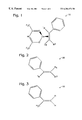
- FIG. 1 is a schematic representation of the present invention precursor with a substituted phenylethylene ligand.
- FIG. 2 is a schematic representation of the substituted phenylethylene ligand.
- FIG. 3 is a schematic representation of the preferred embodiment ⁇ -methylstyrene ligand.
- FIG. 4 is a flowchart illustrating a method for depositing a copper (Cu) seed layer.
- FIG. 5 is a flowchart illustrating one preferred embodiment of the deposition technique of FIG. 4 to form a Cu seed layer on a Cu-receiving surface.
- FIG. 6 is a flowchart illustrating another preferred embodiment of the deposition technique of FIG. 4 to form a Cu seed layer on a Cu-receiving surface.
- FIG. 7 is a schematic block diagram a CVD Cu deposition system sufficient to form Cu films through the methods described in FIGS. 4 - 6 .
- the substituted phenylethylene ligand copper precursor is inexpensive to synthesize. Compared to trimethylvinylsilane, which costs approximately $165 per 100 g, ⁇ -methylstyrene is inexpensive, at approximately $0.60 per 100 g.
- the precursor is stable at room temperature for easy storage and handling. Despite retaining its liquid phase at room temperature, it is highly volatile at higher temperatures. Therefore, no decomposition occurs in the CVD liquid delivery line and vaporizer, which requires precursor stability at 90 degrees C, under vacuum, for four minutes. Further, the precursor has excellent adhesion to metal and metal nitride Cu-receiving substrate surfaces, such as W, Ti, TiN, Ta, TaN, Al, Pt, WN, and similar barrier materials.
- the copper deposited with precursor has low resistivity ( ⁇ 1.9 ⁇ cm), high electromigration resistance, and excellent conformality to severe surface morphology.
- FIG. 1 is a schematic representation of the present invention precursor with a substituted phenylethylene ligand.
- Volatile copper (Cu) precursor compound 10 is used for the chemical vapor deposition (CVD) of copper (Cu) to selected surfaces.
- Precursor compound 10 comprises Cu +1 (hexafluoroacetylacetonate) and a substituted phenylethylene ligand.
- FIG. 2 is a schematic representation of substituted phenylethylene ligand 20 .
- Substituted phenylethylene ligand 20 includes one phenyl group bonded to a first carbon atom, with the remaining bond to the first carbon atom being selected from a first group of potential molecules represented by R 1 .
- the R 1 group consists of C 1 to C 6 alkyl, C 1 to C 6 haloalkyl, phenyl, and C 1 to C 6 alkoxyl.
- the second carbon atom includes a second and third bond selected, respectively, from a second and third group of molecules represented by R 2 and R 3 .
- the second and third bonds, R 2 and R 3 are selected from the group consisting of H, C 1 to C 6 alkyl, phenyl, and C 1 to C 6 alkoxyl.
- the second and third bonds (R 2 and R 3 ) vary independently from each other. In this manner, a stable precursor capable of high Cu deposition rates is formed.
- FIG. 3 is a schematic representation of the preferred embodiment ⁇ -methylstyrene ligand 30 .
- First bond (R 1 ) is H 3 C
- the second bond (R 2 ) is H
- the third bond (R 3 ) is H, whereby an ⁇ -methylstyrene ligand is formed.
- compound 10 includes an additive to create a precursor blend.
- the precursor blend further comprises:
- the blend further comprising the substituted phenylethylene additive having the following structural formula:
- R 1 is selected from the group consisting of C 1 to C 6 alkyl, C 1 to C 6 haloalkyl, phenyl, and C 1 to C 6 alkoxyl;
- R 2 is selected from the group consisting of H, C 1 to C 6 alkyl, phenyl, and C 1 to C 6 alkoxyl;
- R 3 is selected from the group consisting of H, C 1 to C 6 alkyl, phenyl, and C 1 to C 6 alkoxyl, whereby the precursor is further stabilized in a liquid phase.
- the substituted phenylethylene ligand selected to form the precursor is the same substituted phenylethylene ligand used as the additive to form the precursor blend. That is, when the precursor uses an ⁇ -methylstyrene ligand, the additive is also an ⁇ -methylstyrene.
- FIG. 4 is a flowchart illustrating a method for depositing a copper (Cu) seed layer.
- Step 100 provides an integrated circuit (IC) wafer.
- Step 102 volatilizes a Cu precursor compound includes Cu +1 (hexafluoroacetylacetonate), and a substituted phenylethylene ligand including one phenyl group bonded to a first carbon atom.
- the remaining bond to the first carbon atom is selected from a first group consisting of C 1 to C 6 alkyl, C 1 to C 6 haloalkyl, phenyl, and C 1 to C 6 alkoxyl.
- a second carbon atom includes a second and third bond. The second and third bonds are selected from the group consisting of H, C 1 to C 6 alkyl, phenyl, and C 1 to C 6 alkoxyl.
- Step 102 includes the second and third bonds varying independently from each other.
- Step 102 includes the first bond being H 3 C, the second bond being H, and the third bond being H, whereby an ⁇ -methylstyrene ligand is formed.
- Step 100 a includes forming a liquid Cu precursor compound comprising an additive to create a Cu precursor blend.
- the Cu precursor blend further comprises:
- Step 100 a includes the additive having the following structural formula:
- R 1 is selected from the group consisting of C 1 to C 6 alkyl, C 1 to C 6 haloalkyl, phenyl, and C 1 to C 6 alkoxyl.
- R 2 is selected from the group consisting of H, C 1 to C 6 alkyl, C 1 to C 6 phenyl, and C 1 to C 6 alkoxyl.
- R 3 is selected from the group consisting of H, C 1 to C 6 alkyl, phenyl, and C 1 to C 6 alkoxyl, whereby the precursor is further stabilized in a liquid phase.
- Step 100 a includes the substituted phenylethylene ligand of the Cu precursor compound being the same substituted phenylethylene ligand as the additive. So if the precursor compound includes an ⁇ -methylstyrene ligand, the additive is an ⁇ -methylstyrene ligand.
- Step 104 decomposes the Cu precursor compound on a Cu-receiving surface of the IC wafer to form a Cu seed-layer, whereby the seed layer is formed through chemical vapor deposition (CVD).
- Step 106 forms a second layer of Cu overlying the Cu seed layer.
- Step 106 includes depositing the second Cu layer with deposition methods selected from the group consisting of CVD, physical vapor deposition (PVD), and electroplating. That is, once the adhesive seed layer is applied, other more cost effective methods may be used to complete the formation of the copper film.
- Step 108 is a product where the Cu seed layer enhances adhesion between the Cu films and Cu-receiving surface.
- Step 100 provides a chamber having a wafer chuck, on which the IC is mounted.
- Step 100 also provides a showerhead, or equivalent, vapor distribution system. Further steps, detailing the process, precede Step 102 .
- Step 100 b establishes a vaporizing temperature in the range of 60 to 80 degrees C.
- Step 100 c establishes a chuck temperature in the range of approximately 140 to 230 degrees C.
- Step 100 d establishes a chamber pressure in the range of approximately 0.1 to 2 torr (T). A pressure of 0.3 to 1.2 T is generally preferred.
- Step 100 e establishes a distance between the showerhead and the Cu-receiving surface in the range of 15 to 60 millimeters (mm).
- Step 100 f establishes a helium carrier gas flow rate, to carry the Cu precursor compound vapor, in the range of 10 to 400 standard cubic centimeters (sccm). A flow rate of approximately 30 to 150 sccm is generally preferred.
- Step 100 g establishes a liquid precursor flow rate in the range of 0.05 to 0.7 milliliters pre minute (mL/min). A rate of 0.07 to 0.2 is generally preferred. This precursor flow rate assumes a deposition efficiency of approximately 13%.
- Step 102 a establishes a wet helium gas flow rate, to carry water vapor, in the range of approximately 0.1 to 50 sccm. A flow rate of 0.5 to 10 sccm is generally preferred.
- FIG. 5 is a flowchart illustrating one preferred embodiment of the deposition technique of FIG. 4 to form a Cu seed layer on a Cu-receiving surface.
- Step 200 provides a chamber having a wafer chuck to receive an integrated circuit (IC) wafer, and a showerhead to distribute materials on a Cu-receiving surface of the IC wafer.
- Step 202 forms a liquid Cu precursor compound including Cu +1 (hexafluoroacetylacetonate) and an ⁇ -methylstyrene ligand.
- Step 204 adds approximately 5% ⁇ -methylstyrene ligand, as measured by weight ratio of the Cu precursor compound, to create a Cu precursor compound blend.
- Step 206 vaporizes the Cu precursor compound blend at a temperature in the range of approximately 70 to 80 degrees C., with 65 degrees C. being preferred.
- Step 208 heats the wafer chuck to a temperature of approximately 200 degrees C.
- Step 210 creates a chamber pressure of approximately 0.5 T.
- Step 212 carries the vaporized Cu precursor compound blend with a helium carrier gas flow of approximately 100 sccm.
- Step 214 establishes a distance between the showerhead and the Cu-receiving surface of approximately 30 mm. This showerhead distance is effective for a variety of showerheads. This distance would typically be modified when using atypical showerheads or other types of material distribution equipment.
- Step 216 volatilizes the Cu precursor compound blend, which includes the 5% additive.
- Step 218 flows the Cu precursor compound blend at a liquid precursor flow rate in the range of approximately 0.15 mL/min.
- Step 220 carries water vapor with a helium gas flow rate of approximately of 5 sccm.
- Step 222 forms a Cu seed layer on the Cu-receiving surface.
- Step 222 includes depositing the Cu seed layer at a deposition rate of approximately 260 ⁇ per minute.
- Step 222 also includes the deposited Cu seed layer having a resistivity of approximately 2.0 micro-ohms centimeters ( ⁇ cm).
- Step 224 deposits a second layer of Cu film overlying the Cu seed layer.
- Step 224 includes depositing the second Cu layer with deposition methods selected from the group consisting of CVD, physical vapor deposition (PVD), and electroplating.
- Step 226 is a product where a thick Cu film with good adhesive qualities is formed.
- FIG. 6 is a flowchart illustrating another preferred embodiment of the deposition technique of FIG. 4 to form a Cu seed layer on a Cu-receiving surface.
- Step 300 provides a chamber having a wafer chuck to receive an integrated circuit (IC) wafer and a showerhead to distribute materials on a Cu-receiving surface of the IC wafer.
- Step 302 forms a liquid Cu precursor compound including Cu +1 (hexafluoroacetylacetonate) and an ⁇ -methylstyrene ligand.
- Step 304 adds approximately 15% ⁇ -methylstyrene ligand, as measured by weight ratio of the Cu precursor compound, to create a Cu precursor compound blend.
- Step 306 vaporizes the Cu precursor compound blend at a temperature in the range of approximately 65 degrees C.
- Step 308 heats the wafer chuck to a temperature of approximately 190 degrees C.
- Step 310 creates a chamber pressure of approximately 0.7 to 1.2 T.
- Step 312 carries the vaporized Cu precursor compound blend with a helium carrier gas flow of approximately 100 sccm.
- Step 314 establishes a distance between the showerhead and the Cu-receiving surface of approximately 20 mm.
- Step 316 volatilizes the Cu precursor compound blend, including the 15% additive.
- Step 318 flows the Cu precursor compound blend at a liquid precursor flow rate in the range of approximately 0.15 mL/min.
- Step 320 carries water vapor with a helium gas flow rate of approximately of 5 sccm.
- Step 322 forms a Cu seed layer on the Cu-receiving surface.
- Step 322 includes depositing the Cu seed layer at a deposition rate of approximately 150 ⁇ per minute.
- Step 322 includes the deposited Cu seed layer having a resistivity of approximately 2.2 micro-ohms centimeters ( ⁇ cm).
- Step 324 deposits a second layer of Cu film overlying the Cu seed layer.
- Step 324 includes depositing the second Cu layer with deposition methods selected from the group consisting of CVD, physical vapor deposition (PVD), and electroplating.
- Step 326 is a product where a thick Cu film with good adhesive qualities is formed.
- FIG. 7 is a schematic block diagram a CVD Cu deposition system 400 sufficient to form Cu films through the methods described in FIGS. 4-6.
- Liquid precursor compound fills ampoule 402 .
- additive is mixed into the precursor compound.
- a carrier gas typically helium enters ampoule 402 through line 404 and liquid precursor is pushed into line 406 .
- Flow controller 408 regulates the rate of liquid precursor flow.
- Liquid precursor is vaporized in vaporizer 410 , which is heated.
- Carrier gas typically helium, enters the system through line 412 into vaporizer 410 . Vaporized precursor, with the carrier gas, leaves vaporizer 410 through line 414 .
- Carrier gas typically helium
- Carrier gas also enters line 416 , with the gas flow rate being regulated by mass flow controller 418 .
- Carrier gas enters bubbler 420 , where the gas is percolated through liquid water.
- the “wet” helium gas carries water vapor through line 422 .
- the wet helium gas is mixed with vaporized precursor in line 414 .
- the gas mixture in line 414 enters chamber 424 and is distributed through showerhead 426 .
- a wafer 428 mounted on heated chuck 430 , receives the precursor, where it is decomposed to form a Cu film on wafer 428 .
- a pump 434 is used to establish a system vacuum.
- a Cu seed layer deposition method has been disclosed above.
- the S-100TM, ⁇ -methylstyrene ligand, precursor is especially adhesive to typical IC wafer surfaces.
- Forming an adhesive seed layer on the wafer permits the formation of a thicker overlying Cu layer through techniques that are economical or have high deposition rates.
- Other variations and embodiments will occur to those skilled in the art.
Landscapes
- Chemical & Material Sciences (AREA)
- Engineering & Computer Science (AREA)
- Organic Chemistry (AREA)
- General Chemical & Material Sciences (AREA)
- Chemical Kinetics & Catalysis (AREA)
- Materials Engineering (AREA)
- Mechanical Engineering (AREA)
- Metallurgy (AREA)
- Physics & Mathematics (AREA)
- Condensed Matter Physics & Semiconductors (AREA)
- General Physics & Mathematics (AREA)
- Manufacturing & Machinery (AREA)
- Computer Hardware Design (AREA)
- Microelectronics & Electronic Packaging (AREA)
- Power Engineering (AREA)
- Chemical Vapour Deposition (AREA)
- Electrodes Of Semiconductors (AREA)
Priority Applications (7)
| Application Number | Priority Date | Filing Date | Title |
|---|---|---|---|
| US09/351,645 US6204176B1 (en) | 1998-11-10 | 1999-07-12 | Substituted phenylethylene precursor deposition method |
| JP2000581271A JP3729739B2 (ja) | 1998-11-10 | 1999-11-10 | 置換フェニルエチレン前駆体堆積方法 |
| TW088119655A TW518371B (en) | 1998-11-10 | 1999-11-10 | Substituted phenylethylene precursor deposition method |
| PCT/JP1999/006246 WO2000028107A1 (en) | 1998-11-10 | 1999-11-10 | Substituted phenylethylene precursor deposition method |
| DE69915592T DE69915592T2 (de) | 1998-11-10 | 1999-11-10 | BESCHICHTUNGSVERFAHREN ZUR BENUTZUNG EINES Cu(hfac)-VORLÄUFERS MIT EINEM PHENYLETHYLEN-LIGAND |
| EP99971871A EP1047807B1 (en) | 1998-11-10 | 1999-11-10 | A DEPOSITION METHOD FOR USING A Cu(hfac) PRECURSOR WITH A SUBSTITUTED PHENYLETHYLENE LIGAND |
| KR1020007007614A KR100347834B1 (ko) | 1998-11-10 | 1999-11-10 | 치환된 페닐에틸렌 전구체의 퇴적방법 |
Applications Claiming Priority (2)
| Application Number | Priority Date | Filing Date | Title |
|---|---|---|---|
| US10789298P | 1998-11-10 | 1998-11-10 | |
| US09/351,645 US6204176B1 (en) | 1998-11-10 | 1999-07-12 | Substituted phenylethylene precursor deposition method |
Publications (1)
| Publication Number | Publication Date |
|---|---|
| US6204176B1 true US6204176B1 (en) | 2001-03-20 |
Family
ID=26805299
Family Applications (1)
| Application Number | Title | Priority Date | Filing Date |
|---|---|---|---|
| US09/351,645 Expired - Lifetime US6204176B1 (en) | 1998-11-10 | 1999-07-12 | Substituted phenylethylene precursor deposition method |
Country Status (7)
| Country | Link |
|---|---|
| US (1) | US6204176B1 (ja) |
| EP (1) | EP1047807B1 (ja) |
| JP (1) | JP3729739B2 (ja) |
| KR (1) | KR100347834B1 (ja) |
| DE (1) | DE69915592T2 (ja) |
| TW (1) | TW518371B (ja) |
| WO (1) | WO2000028107A1 (ja) |
Cited By (2)
| Publication number | Priority date | Publication date | Assignee | Title |
|---|---|---|---|---|
| US6281589B1 (en) * | 1997-05-22 | 2001-08-28 | Sharp Laboratories Of America, Inc. | System of selectively cleaning copper substrate surfaces, in-situ, to remove copper oxides |
| EP1245695A2 (en) * | 2001-03-27 | 2002-10-02 | Sharp Kabushiki Kaisha | Method for depositing a copper film |
Families Citing this family (1)
| Publication number | Priority date | Publication date | Assignee | Title |
|---|---|---|---|---|
| JP2010209410A (ja) * | 2009-03-10 | 2010-09-24 | Tokyo Electron Ltd | Cu膜の成膜方法および記憶媒体 |
Citations (13)
| Publication number | Priority date | Publication date | Assignee | Title |
|---|---|---|---|---|
| US4385005A (en) | 1981-07-13 | 1983-05-24 | Exxon Research And Engineering Co. | Process for separating unsaturated hydrocarbons using copper or silver complexes with fluorinated diketonates |
| US4425281A (en) | 1981-07-13 | 1984-01-10 | Exxon Research And Engineering Co. | Copper or silver complexes with fluorinated diketones and unsaturated ligands |
| US4434317A (en) | 1983-05-06 | 1984-02-28 | Exxon Research And Engineering Company | Separation and recovery of unsaturated hydrocarbons by copper (I) complexes |
| US5028724A (en) | 1990-03-30 | 1991-07-02 | Air Products And Chemicals, Inc. | Synthesis of volatile fluorinated and non-fluorinated metal-beta-ketonate and metal-beta-ketoiminato complexes |
| US5085731A (en) * | 1991-02-04 | 1992-02-04 | Air Products And Chemicals, Inc. | Volatile liquid precursors for the chemical vapor deposition of copper |
| US5096737A (en) | 1990-10-24 | 1992-03-17 | International Business Machines Corporation | Ligand stabilized +1 metal beta-diketonate coordination complexes and their use in chemical vapor deposition of metal thin films |
| US5098516A (en) * | 1990-12-31 | 1992-03-24 | Air Products And Chemicals, Inc. | Processes for the chemical vapor deposition of copper and etching of copper |
| US5144049A (en) * | 1991-02-04 | 1992-09-01 | Air Products And Chemicals, Inc. | Volatile liquid precursors for the chemical vapor deposition of copper |
| US5187300A (en) * | 1991-02-04 | 1993-02-16 | Air Products And Chemicals, Inc. | Volatile precursors for copper CVD |
| US5273775A (en) * | 1990-09-12 | 1993-12-28 | Air Products And Chemicals, Inc. | Process for selectively depositing copper aluminum alloy onto a substrate |
| US5354712A (en) * | 1992-11-12 | 1994-10-11 | Northern Telecom Limited | Method for forming interconnect structures for integrated circuits |
| US5913147A (en) * | 1997-01-21 | 1999-06-15 | Advanced Micro Devices, Inc. | Method for fabricating copper-aluminum metallization |
| US6001730A (en) * | 1997-10-20 | 1999-12-14 | Motorola, Inc. | Chemical mechanical polishing (CMP) slurry for polishing copper interconnects which use tantalum-based barrier layers |
-
1999
- 1999-07-12 US US09/351,645 patent/US6204176B1/en not_active Expired - Lifetime
- 1999-11-10 KR KR1020007007614A patent/KR100347834B1/ko not_active IP Right Cessation
- 1999-11-10 WO PCT/JP1999/006246 patent/WO2000028107A1/en active IP Right Grant
- 1999-11-10 TW TW088119655A patent/TW518371B/zh not_active IP Right Cessation
- 1999-11-10 DE DE69915592T patent/DE69915592T2/de not_active Expired - Lifetime
- 1999-11-10 EP EP99971871A patent/EP1047807B1/en not_active Expired - Lifetime
- 1999-11-10 JP JP2000581271A patent/JP3729739B2/ja not_active Expired - Fee Related
Patent Citations (13)
| Publication number | Priority date | Publication date | Assignee | Title |
|---|---|---|---|---|
| US4385005A (en) | 1981-07-13 | 1983-05-24 | Exxon Research And Engineering Co. | Process for separating unsaturated hydrocarbons using copper or silver complexes with fluorinated diketonates |
| US4425281A (en) | 1981-07-13 | 1984-01-10 | Exxon Research And Engineering Co. | Copper or silver complexes with fluorinated diketones and unsaturated ligands |
| US4434317A (en) | 1983-05-06 | 1984-02-28 | Exxon Research And Engineering Company | Separation and recovery of unsaturated hydrocarbons by copper (I) complexes |
| US5028724A (en) | 1990-03-30 | 1991-07-02 | Air Products And Chemicals, Inc. | Synthesis of volatile fluorinated and non-fluorinated metal-beta-ketonate and metal-beta-ketoiminato complexes |
| US5273775A (en) * | 1990-09-12 | 1993-12-28 | Air Products And Chemicals, Inc. | Process for selectively depositing copper aluminum alloy onto a substrate |
| US5096737A (en) | 1990-10-24 | 1992-03-17 | International Business Machines Corporation | Ligand stabilized +1 metal beta-diketonate coordination complexes and their use in chemical vapor deposition of metal thin films |
| US5098516A (en) * | 1990-12-31 | 1992-03-24 | Air Products And Chemicals, Inc. | Processes for the chemical vapor deposition of copper and etching of copper |
| US5144049A (en) * | 1991-02-04 | 1992-09-01 | Air Products And Chemicals, Inc. | Volatile liquid precursors for the chemical vapor deposition of copper |
| US5187300A (en) * | 1991-02-04 | 1993-02-16 | Air Products And Chemicals, Inc. | Volatile precursors for copper CVD |
| US5085731A (en) * | 1991-02-04 | 1992-02-04 | Air Products And Chemicals, Inc. | Volatile liquid precursors for the chemical vapor deposition of copper |
| US5354712A (en) * | 1992-11-12 | 1994-10-11 | Northern Telecom Limited | Method for forming interconnect structures for integrated circuits |
| US5913147A (en) * | 1997-01-21 | 1999-06-15 | Advanced Micro Devices, Inc. | Method for fabricating copper-aluminum metallization |
| US6001730A (en) * | 1997-10-20 | 1999-12-14 | Motorola, Inc. | Chemical mechanical polishing (CMP) slurry for polishing copper interconnects which use tantalum-based barrier layers |
Non-Patent Citations (8)
| Title |
|---|
| "MOCVD of Copper from the Solution of New and Liquid Precursor" by H.K. Shin, Y.H. Cho, D.J. Yoo, H.J. Shin & E.S. Lee published in Mat. Res. Soc. Symp Proc. vol. 514. Abstract Only. |
| Article entitled "Chemical Vapor Deposited Copper from Alkyne Stabilized Copper(I) Hexafluoroacetylacetonate Complexes", by T.H. Baum and C.E. Larson, published in J. Electrochem. Soc. vol. 140, No. 1 Jan. 1993, pp. 154-158. |
| Article entitled "Copper(I) tertt-Butly 3-Oxobutanoate Complexes as Precursors for Chemical Vapor Deposition of Copper", by H Choi and S. Hwang, published in Chem. Mater. 1998, 10, pp. 2326-2328. |
| Article entitled, "Alkene and Carbon Monoxide Derivatives of Copper(I) and Silver(I), etc.", by G. Doyle, K.A. Eriksen & D. Van Engen, published in Organometallics 1985, pp. 830-835. |
| Article entitled, "Hot-Wall Chemical Vapor Deposition of Copper from Copper(I) Compounds. 2. Selective, Low-Temperature Deposition of Copper from Copper(I), etc." by H.K. Shin, K.M. Chi, M.J. Hampden-Smith, T.T. Kodas, J.D. Farr & M. Paffett, published in Chem. Mater.1992, 4, pp. 788-795. |
| Article entitled, "Low-Temperature Chemical Vapor Deposition of High-Purity Copper from an Organometallic source", by D.B. Beach, F.K. LeGoues & C.K. Hu, published in Chem. Mater.;1990, pp. 216-219. |
| C. Y. Chang and S. M. Sze, VLSI Technology, 1996, McGraw-Hill Companies, Inc., pp. 389-391.* |
| Stanley Wolf, Silicon Processing for the VLSI Era vol. 2: Process Integration, 1990, Lattice Press, p. 193.* |
Cited By (5)
| Publication number | Priority date | Publication date | Assignee | Title |
|---|---|---|---|---|
| US6281589B1 (en) * | 1997-05-22 | 2001-08-28 | Sharp Laboratories Of America, Inc. | System of selectively cleaning copper substrate surfaces, in-situ, to remove copper oxides |
| EP1245695A2 (en) * | 2001-03-27 | 2002-10-02 | Sharp Kabushiki Kaisha | Method for depositing a copper film |
| US6596344B2 (en) * | 2001-03-27 | 2003-07-22 | Sharp Laboratories Of America, Inc. | Method of depositing a high-adhesive copper thin film on a metal nitride substrate |
| EP1245695A3 (en) * | 2001-03-27 | 2004-01-07 | Sharp Kabushiki Kaisha | Method for depositing a copper film |
| KR100479519B1 (ko) * | 2001-03-27 | 2005-03-30 | 샤프 가부시키가이샤 | 고접착성 구리 박막을 금속 질화물 기판 상에 증착시키는방법 |
Also Published As
| Publication number | Publication date |
|---|---|
| KR100347834B1 (ko) | 2002-08-07 |
| JP3729739B2 (ja) | 2005-12-21 |
| JP2002529602A (ja) | 2002-09-10 |
| DE69915592D1 (de) | 2004-04-22 |
| EP1047807A1 (en) | 2000-11-02 |
| WO2000028107A1 (en) | 2000-05-18 |
| DE69915592T2 (de) | 2005-02-03 |
| EP1047807B1 (en) | 2004-03-17 |
| KR20010034018A (ko) | 2001-04-25 |
| TW518371B (en) | 2003-01-21 |
Similar Documents
| Publication | Publication Date | Title |
|---|---|---|
| US5744192A (en) | Method of using water vapor to increase the conductivity of cooper desposited with cu(hfac)TMVS | |
| EP0854507B1 (en) | Precursor with (alkoxy) (alkyl) vinylsilane ligand to deposit copper and method for the same | |
| EP0852229B1 (en) | Precursor with (methoxy) (methyl) silylolefin ligands to deposit copper and method for the same | |
| US6090963A (en) | Alkene ligand precursor and synthesis method | |
| US5994571A (en) | Substituted ethylene precursor and synthesis method | |
| US6204176B1 (en) | Substituted phenylethylene precursor deposition method | |
| KR100346562B1 (ko) | 물을 첨가하여 Cu의 도전율을 향상시키는 Cu(hfac)TMVS 전구체 | |
| US6015918A (en) | Allyl-derived precursor and synthesis method | |
| US6245261B1 (en) | Substituted phenylethylene precursor and synthesis method | |
| EP0855399B1 (en) | Precursor with alkylaminosilylolefin ligands to deposit copper and method for same | |
| EP1000948B1 (en) | Copper containing substituted phenylethylene precursor and synthesis method | |
| EP0987346A1 (en) | Copper deposition method using a precursor with (alkyloxy) (alkyl)silylolefin ligands |
Legal Events
| Date | Code | Title | Description |
|---|---|---|---|
| AS | Assignment |
Owner name: SHARP LABORATORIES OF AMERICA, INC., WASHINGTON Free format text: ASSIGNMENT OF ASSIGNORS INTEREST;ASSIGNORS:ZHUANG, WEI-WEI;CHARNESKI, LAWRENCE J.;HSU, SHENG TENG;REEL/FRAME:010105/0130 Effective date: 19990712 |
|
| STCF | Information on status: patent grant |
Free format text: PATENTED CASE |
|
| AS | Assignment |
Owner name: SHARP KABUSHIKI KAISHA, JAPAN Free format text: ASSIGNMENT OF ASSIGNORS INTEREST;ASSIGNOR:SHARP LABORATORIES OF AMERICA, INC.;REEL/FRAME:012946/0165 Effective date: 20020514 |
|
| FPAY | Fee payment |
Year of fee payment: 4 |
|
| FPAY | Fee payment |
Year of fee payment: 8 |
|
| FPAY | Fee payment |
Year of fee payment: 12 |