US6069810A - Method for reducing feedbacks on a flow of current drawn from a network during operation of inductive load and a booster converter for driving motors in accordance with the method - Google Patents
Method for reducing feedbacks on a flow of current drawn from a network during operation of inductive load and a booster converter for driving motors in accordance with the method Download PDFInfo
- Publication number
- US6069810A US6069810A US09/036,213 US3621398A US6069810A US 6069810 A US6069810 A US 6069810A US 3621398 A US3621398 A US 3621398A US 6069810 A US6069810 A US 6069810A
- Authority
- US
- United States
- Prior art keywords
- diode
- electronic switch
- motor
- booster converter
- motor winding
- Prior art date
- Legal status (The legal status is an assumption and is not a legal conclusion. Google has not performed a legal analysis and makes no representation as to the accuracy of the status listed.)
- Expired - Lifetime
Links
- 238000000034 method Methods 0.000 title claims abstract description 25
- 230000001939 inductive effect Effects 0.000 title claims abstract description 14
- 238000004804 winding Methods 0.000 claims abstract description 82
- 238000001914 filtration Methods 0.000 claims abstract description 7
- 239000003990 capacitor Substances 0.000 claims description 39
- 230000005415 magnetization Effects 0.000 claims description 3
- 238000010586 diagram Methods 0.000 description 10
- 238000011045 prefiltration Methods 0.000 description 4
- 230000001105 regulatory effect Effects 0.000 description 3
- 238000009499 grossing Methods 0.000 description 2
- 230000002411 adverse Effects 0.000 description 1
- 230000005347 demagnetization Effects 0.000 description 1
- 230000001419 dependent effect Effects 0.000 description 1
- 238000012986 modification Methods 0.000 description 1
- 230000004048 modification Effects 0.000 description 1
Images

Classifications
-
- H—ELECTRICITY
- H02—GENERATION; CONVERSION OR DISTRIBUTION OF ELECTRIC POWER
- H02M—APPARATUS FOR CONVERSION BETWEEN AC AND AC, BETWEEN AC AND DC, OR BETWEEN DC AND DC, AND FOR USE WITH MAINS OR SIMILAR POWER SUPPLY SYSTEMS; CONVERSION OF DC OR AC INPUT POWER INTO SURGE OUTPUT POWER; CONTROL OR REGULATION THEREOF
- H02M1/00—Details of apparatus for conversion
- H02M1/42—Circuits or arrangements for compensating for or adjusting power factor in converters or inverters
- H02M1/4208—Arrangements for improving power factor of AC input
-
- H—ELECTRICITY
- H02—GENERATION; CONVERSION OR DISTRIBUTION OF ELECTRIC POWER
- H02H—EMERGENCY PROTECTIVE CIRCUIT ARRANGEMENTS
- H02H9/00—Emergency protective circuit arrangements for limiting excess current or voltage without disconnection
- H02H9/02—Emergency protective circuit arrangements for limiting excess current or voltage without disconnection responsive to excess current
-
- H—ELECTRICITY
- H02—GENERATION; CONVERSION OR DISTRIBUTION OF ELECTRIC POWER
- H02H—EMERGENCY PROTECTIVE CIRCUIT ARRANGEMENTS
- H02H7/00—Emergency protective circuit arrangements specially adapted for specific types of electric machines or apparatus or for sectionalised protection of cable or line systems, and effecting automatic switching in the event of an undesired change from normal working conditions
- H02H7/20—Emergency protective circuit arrangements specially adapted for specific types of electric machines or apparatus or for sectionalised protection of cable or line systems, and effecting automatic switching in the event of an undesired change from normal working conditions for electronic equipment
-
- H—ELECTRICITY
- H02—GENERATION; CONVERSION OR DISTRIBUTION OF ELECTRIC POWER
- H02M—APPARATUS FOR CONVERSION BETWEEN AC AND AC, BETWEEN AC AND DC, OR BETWEEN DC AND DC, AND FOR USE WITH MAINS OR SIMILAR POWER SUPPLY SYSTEMS; CONVERSION OF DC OR AC INPUT POWER INTO SURGE OUTPUT POWER; CONTROL OR REGULATION THEREOF
- H02M1/00—Details of apparatus for conversion
- H02M1/42—Circuits or arrangements for compensating for or adjusting power factor in converters or inverters
- H02M1/4208—Arrangements for improving power factor of AC input
- H02M1/4258—Arrangements for improving power factor of AC input using a single converter stage both for correction of AC input power factor and generation of a regulated and galvanically isolated DC output voltage
-
- H—ELECTRICITY
- H02—GENERATION; CONVERSION OR DISTRIBUTION OF ELECTRIC POWER
- H02M—APPARATUS FOR CONVERSION BETWEEN AC AND AC, BETWEEN AC AND DC, OR BETWEEN DC AND DC, AND FOR USE WITH MAINS OR SIMILAR POWER SUPPLY SYSTEMS; CONVERSION OF DC OR AC INPUT POWER INTO SURGE OUTPUT POWER; CONTROL OR REGULATION THEREOF
- H02M3/00—Conversion of DC power input into DC power output
- H02M3/02—Conversion of DC power input into DC power output without intermediate conversion into AC
- H02M3/04—Conversion of DC power input into DC power output without intermediate conversion into AC by static converters
- H02M3/10—Conversion of DC power input into DC power output without intermediate conversion into AC by static converters using discharge tubes with control electrode or semiconductor devices with control electrode
- H02M3/145—Conversion of DC power input into DC power output without intermediate conversion into AC by static converters using discharge tubes with control electrode or semiconductor devices with control electrode using devices of a triode or transistor type requiring continuous application of a control signal
- H02M3/155—Conversion of DC power input into DC power output without intermediate conversion into AC by static converters using discharge tubes with control electrode or semiconductor devices with control electrode using devices of a triode or transistor type requiring continuous application of a control signal using semiconductor devices only
- H02M3/1555—Conversion of DC power input into DC power output without intermediate conversion into AC by static converters using discharge tubes with control electrode or semiconductor devices with control electrode using devices of a triode or transistor type requiring continuous application of a control signal using semiconductor devices only for the generation of a regulated current to a load whose impedance is substantially inductive
-
- H—ELECTRICITY
- H02—GENERATION; CONVERSION OR DISTRIBUTION OF ELECTRIC POWER
- H02M—APPARATUS FOR CONVERSION BETWEEN AC AND AC, BETWEEN AC AND DC, OR BETWEEN DC AND DC, AND FOR USE WITH MAINS OR SIMILAR POWER SUPPLY SYSTEMS; CONVERSION OF DC OR AC INPUT POWER INTO SURGE OUTPUT POWER; CONTROL OR REGULATION THEREOF
- H02M3/00—Conversion of DC power input into DC power output
- H02M3/02—Conversion of DC power input into DC power output without intermediate conversion into AC
- H02M3/04—Conversion of DC power input into DC power output without intermediate conversion into AC by static converters
- H02M3/10—Conversion of DC power input into DC power output without intermediate conversion into AC by static converters using discharge tubes with control electrode or semiconductor devices with control electrode
- H02M3/145—Conversion of DC power input into DC power output without intermediate conversion into AC by static converters using discharge tubes with control electrode or semiconductor devices with control electrode using devices of a triode or transistor type requiring continuous application of a control signal
- H02M3/155—Conversion of DC power input into DC power output without intermediate conversion into AC by static converters using discharge tubes with control electrode or semiconductor devices with control electrode using devices of a triode or transistor type requiring continuous application of a control signal using semiconductor devices only
- H02M3/156—Conversion of DC power input into DC power output without intermediate conversion into AC by static converters using discharge tubes with control electrode or semiconductor devices with control electrode using devices of a triode or transistor type requiring continuous application of a control signal using semiconductor devices only with automatic control of output voltage or current, e.g. switching regulators
-
- Y—GENERAL TAGGING OF NEW TECHNOLOGICAL DEVELOPMENTS; GENERAL TAGGING OF CROSS-SECTIONAL TECHNOLOGIES SPANNING OVER SEVERAL SECTIONS OF THE IPC; TECHNICAL SUBJECTS COVERED BY FORMER USPC CROSS-REFERENCE ART COLLECTIONS [XRACs] AND DIGESTS
- Y02—TECHNOLOGIES OR APPLICATIONS FOR MITIGATION OR ADAPTATION AGAINST CLIMATE CHANGE
- Y02B—CLIMATE CHANGE MITIGATION TECHNOLOGIES RELATED TO BUILDINGS, e.g. HOUSING, HOUSE APPLIANCES OR RELATED END-USER APPLICATIONS
- Y02B70/00—Technologies for an efficient end-user side electric power management and consumption
- Y02B70/10—Technologies improving the efficiency by using switched-mode power supplies [SMPS], i.e. efficient power electronics conversion e.g. power factor correction or reduction of losses in power supplies or efficient standby modes
-
- Y—GENERAL TAGGING OF NEW TECHNOLOGICAL DEVELOPMENTS; GENERAL TAGGING OF CROSS-SECTIONAL TECHNOLOGIES SPANNING OVER SEVERAL SECTIONS OF THE IPC; TECHNICAL SUBJECTS COVERED BY FORMER USPC CROSS-REFERENCE ART COLLECTIONS [XRACs] AND DIGESTS
- Y02—TECHNOLOGIES OR APPLICATIONS FOR MITIGATION OR ADAPTATION AGAINST CLIMATE CHANGE
- Y02P—CLIMATE CHANGE MITIGATION TECHNOLOGIES IN THE PRODUCTION OR PROCESSING OF GOODS
- Y02P80/00—Climate change mitigation technologies for sector-wide applications
- Y02P80/10—Efficient use of energy, e.g. using compressed air or pressurized fluid as energy carrier
Definitions
- the present invention relates to a method of reducing feedbacks on a temporary flow of current drawn from a network, during an operation of an inductive load, with a rectifying circuit, wherein the method including active filtering of harmonics of a network fundamental component with a booster converter.
- the present invention also relates to a booster converter implementing the method according to the present invention.
- the network a.c. voltage is rectified and is smoothed, e.g., with a capacitor.
- the d.c. voltage becomes more or less ripple, and the temporary flow of the current drawn from the network substantially deviates from a sinusoidal shape and has a relatively high harmonic component.
- the so-called network feedbacks obviously depend on a type of the load and its current consumption.
- Mandatory standards prescribe threshold values or threshold curves for an allowable harmonic component dependent on the operating current.
- filter circuits are used which are connected between a network rectifier and the load.
- a known active filter circuit is shown in FIG. 6.
- a so-called booster converter and a power factor control circuit make it possible to draw from a network, within allowable power limits and independent of possible variations of the load, current of an approximately sinusoidal shape.
- the booster converter includes connected, between the output of a network rectifier (6) with a smoothing capacitor (4) and a further smoothing capacitor (5), a choke (1) (a high set-up choke), a diode (3), and a shunt arm of a capacitor (5).
- the known network feedback filter presents a problem when the available space is limited and when an apparatus, in particular, a hand-held tool is required to have the smallest possible weight. This is because the choke requires a relatively large and heavy core layout, in particular for drawing a greater power from the network.
- the choke In the circuit shown in FIG. 6, the choke (1) conducts a d.c. network current. Therefore, the choke should be designed magnetically for a highest current magnitude, i.e., for a maximal amplitude plus a superimposed ripple.
- an object of the present invention is to provide a method and a power feed circuit which reliably prevent undesirable feedbacks, which act, via the rectifier, on a temporary flow drawn from a network current during operation of an inductive load, wherein the method and the power feed circuit include a filter arrangement having definite advantages with regard to technical expenditures and weight in comparison with conventional network feedback filtering circuits.
- the technical principle which forms a basis of the present invention, is based on a recognition that the function of the choke of an active network feedback filter can be taken up, in a circuit according to FIG. 6, by an inductive load without adversely affecting the function of the load, e.g., by providing one or more a motor windings when a motor forms the inductive load.
- a booster converter which implements the inventive method, can be used for driving different motors.
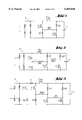
- FIG. 1 shows a circuit diagram of a power feed circuit with a rectifying circuit and a booster converter for electric motors, in which the choke function is taken up by a motor winding in accordance with the invention
- FIG. 2 shows a circuit diagram of a power feed circuit with a rectifying circuit and a booster converter for electric motors, in which the choke function is taken up by two motor windings, in accordance with the invention
- FIG. 3 shows a circuit diagram of a power feed circuit with a rectifying circuit and a booster converter according to the present together with an auxiliary choke, for electric motors, in which the function of an original choke is taken up by a single motor winding only partially in accordance with the invention
- FIG. 4 shows a circuit diagram of a power feed circuit with a rectifying circuit and a booster converter together with an auxiliary choke, for electric motors, in which the function of an original choke is taken up by two motor windings only partially, in accordance with the invention
- FIG. 5 shows a simplified circuit diagram of a power feed circuit with a rectifying circuit and a booster converter, together with an auxiliary choke, for electric motors, with which the function of an original choke is taken up by two motor winding in accordance with the invention
- FIG. 6 shows a principle circuit diagram of a power feed circuit with a rectifying circuit, a booster converter and a prefilter.
- FIG. 1 shows a circuit diagram of a power feed circuit including a rectifying circuit 6 and a booster converter according to the present invention for electric motors, in which the choke function is taken up by a motor windings MW1.
- the motor winding MW1 is driven via a bridge circuit which includes, as a first branch, a series connection of a first diode D1 and a first transistor T1 the emitter of which is connected with the cathode of the diode D1.
- the anode of the first diode D1 is connected with the ground, and the collector of the first transistor T1 is connected with the distribution voltage.
- the base of the first transistor T1 is connected with a control circuit (not shown).
- the second branch of the bridge circuit is formed by a series connection of a second diode D2 and of a second transistor T2 the collector of which is connected with the anode of the second diode D2.
- the cathode of the second diode D2 is connected via a collector-emitter route of a transistor TB with the distribution voltage, and the emitter of the second transistor T2 is connected with the ground.
- the base of the second transistor T2 is connected with the control circuit.
- the motor winding MW1 taps the bridge circuit voltage between connection points of the first transistor T1 and the first diode D1 and the second transistor T2 and the second diode D2, respectively.
- the base of the transistor TB like the bases of the first and second transistors T1 and T2, is also connected with the control circuit.
- the booster converter includes further a capacitor 5 which is connected parallel to the branch of the bridge circuit formed by the second diode D2 and the second transistor T2.
- the motor winding is magnetized, in a first phase, with a high capacitor voltage of the capacitor 5 via the first transistor T1, the second transistor T2 and the transistor TB of the booster converter.
- the magnetization is terminated, in a second phase, the transistor TB of the booster converter is blocked, while the second transistor T2 is clocked with a pulse width modulation by the control circuit, and the first transistor T1 remains in a conductive state.
- the motor winding MW1 is also used for correction of the power factor.
- the control circuit directly controls the first transistor T1, the second transistor T2, and the transistor TB.
- FIG. 2 shows a circuit diagram of a power feed circuit including a rectifying circuit 6 and a booster converter for electric motors, in which the choke function is taken up by two motor windings TW1 and TW2.
- the two motor windings MW1 and MW2 are driven via a bridge circuit that includes two connected in parallel second branches, with the motor windings MW1 and MW2 being connected between a connection point of the first diode D1 and the first transistor T1 and, respectively, between connection points of the second diode D2 and the second transistor T2 and another second diode D2* and second transistor T2*.
- the base of the another second transistor T2*, as the base of the second transistor T2 is also connected with the control circuit.
- the motor winding MW1 is magnetized with the high capacitor voltage of the capacitor 5 via the first transistor T1, the second transistor T2 and the transistor TB while the current in the motor winding MW2 can flow freely through the transistor T1, the another second diode D2* and the transistor TB, whereby the motor winding MW2 is demagnetized.
- the motor winding MW2 is magnetized with the high capacitor voltage of the capacitor 5 via the first transistor T1, the another second transistor T2* and the booster converter transistor TB, while the current in the motor winding MW1 can flow freely via the first transistor T1, the second diode D2 and the transistor TB, whereby the motor winding MW1 is demagnetized.
- the second transistors T2 and T2* are clocked alternatively with a pulse width modulation when the respective motor windings MW1, MW2, which are controlled via these transistors, are magnetized. Accordingly, the motor windings MW1 and MW2 can be used for correction of the power factor.
- a particular advantage of this embodiment consists in that the control circuit, which is not shown, does not require any additional significant expenses associated with additional control and regulating functions.
- FIG. 3 shows a circuit diagram of a power feed circuit with the rectifying circuit 6 and the inventive booster converter for the electric motors in which the choke function is taken up by the motor winding MW1 and an auxiliary choke Dr1.
- the circuit shown in FIG. 3 includes, in addition to the elements corresponding to those of the circuit shown in FIG. 1, a third diode 3, connected, in series, in the flow direction between the distribution voltage and the motor driving bridge circuit, and an additional bridge circuit the bridge voltage of which it tapped from an auxiliary choke Dr 1.
- the additional bridge circuit has, as a first branch, a series connection of a fourth diode Dh1 with a fourth transistor Th1 the emitter of which is connected with a cathode of the diode Dh1.
- the anode of the fourth diode Dh1 is connected with the ground, and the collector of the fourth transistor Th1 is connected with a connection point of the distribution voltage and the anode of the third diode 3.
- the second branch of the additional bridge circuit is formed of a series connection of a fifth diode Dh2 and a fifth transistor Th2 the collector of which is connected with the anode of the fifth diode Dh2.
- the cathode of the fifth diode Dh2 is connected, via a collector-emitter route of the third transistor TB of the booster converter, with the distribution voltage the emitter of the fifth transistor Th2 is connected with the ground.
- the auxiliary choke Dh1 is connected between the connection point of the fourth transistor Th1 and the fourth diode Dh1 and the connection point of the fifth transistor Th2 and the fifth diode Dh2.
- the bases of the fourth and fifth transistors Th2l and Th2, like those of the first and second transistors T1 and T2, are connected with the control circuit.
- the motor winding MW1 is connected as it is connected in the embodiment of FIG. 1.
- the auxiliary choke Dr1 is magnetized via the fourth transistor Th1 and the fifth transistor Th2 which is clocked with pulse width modulation.
- FIG. 4 shows a circuit diagram of a power feed circuit with the rectifying circuit 6 and the inventive booster converter with an auxiliary choke Dr1 for the motor, with which the function of an original choke is taken up to a large extent by two motor windings MW1 and MW2.
- the bridge circuit for driving the motor winding MW1 and the third transistor TB is connected parallel to a second bridge circuit for driving the second motor winding and another third transistor TB*. Both motor windings MW1 and MW2 are wired in the same manner.
- the transistors T1* and T2* of the second bridge circuit and the third transistor TB* are controlled in the same way as the corresponding transistors T1, T2 and TB.
- the motor windings MW1 and MW2 are connected in the same way as in the embodiment of FIG. 2.
- the auxiliary choke Dr1 is clocked with pulse width modulation through the fourth and fifth transistors Th1 and Th2 and is also magnetized.
- the motor winding MW1 When the motor winding MW1 is magnetized with the high capacitor voltage of the capacitor 5 via the first transistor T1, the second transistor and the third transistor TB, the current in the motor winding MW2 can flow freely for a long time via the transistor T1*, diode D2* and the transistor TB, or the motor winding MW2 can be rapidly demagnetized via diodes D1*, D2* and the capacitor 5.
- the current in the motor winding MW1 can flow freely via the transistor T1, the diode D2 and the transistor TB, or the motor winding MW1 can be demagnetized via the diodes D1 and D2 and the capacitor 5 while the motor winding MW2 is magnetized with the high capacitor voltage of the capacitor 5 via the first transistor T1*, the second transistor T2* of the second bridge circuit as well as through the transistor TB*.
- the auxiliary choke Dr1 in comparison with a choke of a conventional booster, can be designed for handling a current about 70% smaller. Also, a necessary prefilter, can also be made smaller than in a circuit without an auxiliary choke.
- the circuit of FIG. 2 can so be wired with, the aid of an electronic switch (TB* and T1*), in the same way as the circuit of FIG. 4, such that respective motor windings are rapidly demagnetized, with the transistor TB being switch on (or being in a conductive state), over the capacitor 5 and not over the transistor TB.
- an electronic switch TB* and T1*
- the above-described circuits can also be changed such that the fourth transistor Th1 is replaced by a short circuit impedance, and the fourth diode Dh1 is replaced by a no-load.
- This change for the circuit shown in FIG. 4, is represented by the circuit shown in FIG. 5.
- a further simplification of the previously described circuit embodiments is achieved by replacing first diodes D1, D1* by a no-load.
Landscapes
- Engineering & Computer Science (AREA)
- Power Engineering (AREA)
- Dc-Dc Converters (AREA)
- Rectifiers (AREA)
- Control Of Direct Current Motors (AREA)
- Power Conversion In General (AREA)
Applications Claiming Priority (2)
| Application Number | Priority Date | Filing Date | Title |
|---|---|---|---|
| DE19709264 | 1997-03-06 | ||
| DE19709264A DE19709264A1 (de) | 1997-03-06 | 1997-03-06 | Verfahren zur Reduzierung von Rückwirkungen auf den Verlauf des einem Netz entnommenen Stroms bei induktiven Lasten und Vorrichtung zum Antreiben von Motoren nach diesem Verfahren |
Publications (1)
| Publication Number | Publication Date |
|---|---|
| US6069810A true US6069810A (en) | 2000-05-30 |
Family
ID=7822492
Family Applications (1)
| Application Number | Title | Priority Date | Filing Date |
|---|---|---|---|
| US09/036,213 Expired - Lifetime US6069810A (en) | 1997-03-06 | 1998-03-06 | Method for reducing feedbacks on a flow of current drawn from a network during operation of inductive load and a booster converter for driving motors in accordance with the method |
Country Status (5)
| Country | Link |
|---|---|
| US (1) | US6069810A (enExample) |
| EP (1) | EP0869605B1 (enExample) |
| JP (1) | JP4188444B2 (enExample) |
| KR (1) | KR19980079709A (enExample) |
| DE (2) | DE19709264A1 (enExample) |
Cited By (9)
| Publication number | Priority date | Publication date | Assignee | Title |
|---|---|---|---|---|
| US6256211B1 (en) * | 1998-12-31 | 2001-07-03 | Stmicroelectronics S.R.L. | Circuit device for driving an a.c. electric load |
| WO2002015374A1 (de) * | 2000-08-14 | 2002-02-21 | Braun Gmbh | Schaltungsanordnung und elektrogerät mit einer induktiven last und einem drosselwandler |
| US6469485B2 (en) | 2000-07-07 | 2002-10-22 | Honeywell International Inc. | Active filter and method for suppressing current harmonics |
| WO2005071823A1 (de) * | 2004-01-27 | 2005-08-04 | Robert Bosch Gmbh | Modul und verfahren zum verändern der drehzahl eines motors |
| US20090201620A1 (en) * | 2008-02-08 | 2009-08-13 | Restech Limited | Electromagnetic field energy recycling |
| WO2009099342A3 (en) * | 2008-02-08 | 2009-10-22 | Restech Limited | Electromagnetic field energy recycling |
| US20100059023A1 (en) * | 2007-01-09 | 2010-03-11 | Continental Automotive Gmbh | Circuit Arrangement and Method for Operating an Inductive Load |
| US20100315027A1 (en) * | 2009-06-04 | 2010-12-16 | Ralph Wystup | Procedures and Control System to Control a Brushless Electric Motor |
| WO2011016734A1 (en) * | 2009-08-05 | 2011-02-10 | Restech Limited | Electromagnetic field energy recycling |
Families Citing this family (6)
| Publication number | Priority date | Publication date | Assignee | Title |
|---|---|---|---|---|
| GB9906716D0 (en) * | 1999-03-23 | 1999-05-19 | Switched Reluctance Drives Ltd | Operation of a switched reluctance machine from dual supply voltages |
| DE10021785A1 (de) * | 2000-05-04 | 2001-12-06 | Hilti Ag | Gleichstromspeiseschaltung für Induktivitäten |
| KR100704482B1 (ko) * | 2005-04-01 | 2007-04-09 | 엘지전자 주식회사 | 저속 영역과 고속 영역에서의 발전 효율이 개선된 에스알발전기 |
| DE102008043043A1 (de) * | 2008-10-22 | 2010-04-29 | Robert Bosch Gmbh | Leistungsendstufe für einen Pulswechselrichter |
| DE102008053679B3 (de) * | 2008-10-29 | 2010-01-28 | Forschungszentrum Karlsruhe Gmbh | Stromversorgung und Verfahren für eine gepulst betriebene induktive Last |
| KR101069140B1 (ko) * | 2011-05-26 | 2011-09-30 | 주식회사 자이벡 | 권선형 유도 전동기의 전력 회생 장치 |
Citations (3)
| Publication number | Priority date | Publication date | Assignee | Title |
|---|---|---|---|---|
| US4386299A (en) * | 1979-12-20 | 1983-05-31 | Societe Anonyme Dite: Alsthom-Atlantique | Electronic control circuit for a separately excited DC machine |
| US5146398A (en) * | 1991-08-20 | 1992-09-08 | Led Corporation N.V. | Power factor correction device provided with a frequency and amplitude modulated boost converter |
| US5563487A (en) * | 1994-04-22 | 1996-10-08 | Switched Reluctance Drives, Ltd. | Control circuit for an inductive load |
Family Cites Families (7)
| Publication number | Priority date | Publication date | Assignee | Title |
|---|---|---|---|---|
| EP0178615A3 (en) * | 1984-10-19 | 1987-08-05 | Kollmorgen Corporation | Power supply systems for inductive elements |
| JPH03293993A (ja) * | 1990-04-06 | 1991-12-25 | Fanuc Ltd | 可変リラクタンスモータの駆動方式 |
| US5115181A (en) * | 1990-10-05 | 1992-05-19 | Emerson Electric Co. | Power converter for a switched reluctance motor |
| US5224025A (en) * | 1992-04-21 | 1993-06-29 | Wisconsin Alumni Research Foundation | Forward converter with two active switches and unity power factor capability |
| GB9225090D0 (en) * | 1992-12-01 | 1993-01-20 | Univ Cardiff | Performance enhancement of single phase switched motor by d c link voltage |
| DE4428682C2 (de) * | 1994-08-12 | 1997-01-23 | Robert Seuffer Gmbh & Co | Verfahren zur Versorgung einer induktiven Last mit sinusförmigem Wechselstrom und Wechselstromsteller hierfür |
| FR2743955B1 (fr) * | 1996-01-22 | 1998-04-10 | Moulinex Sa | Procede pour alimenter un moteur a reluctance variable a commutation electronique et circuit d'alimentation pour sa mise en oeuvre |
-
1997
- 1997-03-06 DE DE19709264A patent/DE19709264A1/de not_active Ceased
-
1998
- 1998-01-22 EP EP98810032A patent/EP0869605B1/de not_active Expired - Lifetime
- 1998-01-22 DE DE59802191T patent/DE59802191D1/de not_active Expired - Fee Related
- 1998-02-11 KR KR1019980004013A patent/KR19980079709A/ko not_active Withdrawn
- 1998-03-06 JP JP05538898A patent/JP4188444B2/ja not_active Expired - Fee Related
- 1998-03-06 US US09/036,213 patent/US6069810A/en not_active Expired - Lifetime
Patent Citations (3)
| Publication number | Priority date | Publication date | Assignee | Title |
|---|---|---|---|---|
| US4386299A (en) * | 1979-12-20 | 1983-05-31 | Societe Anonyme Dite: Alsthom-Atlantique | Electronic control circuit for a separately excited DC machine |
| US5146398A (en) * | 1991-08-20 | 1992-09-08 | Led Corporation N.V. | Power factor correction device provided with a frequency and amplitude modulated boost converter |
| US5563487A (en) * | 1994-04-22 | 1996-10-08 | Switched Reluctance Drives, Ltd. | Control circuit for an inductive load |
Cited By (14)
| Publication number | Priority date | Publication date | Assignee | Title |
|---|---|---|---|---|
| US6256211B1 (en) * | 1998-12-31 | 2001-07-03 | Stmicroelectronics S.R.L. | Circuit device for driving an a.c. electric load |
| US6469485B2 (en) | 2000-07-07 | 2002-10-22 | Honeywell International Inc. | Active filter and method for suppressing current harmonics |
| WO2002015374A1 (de) * | 2000-08-14 | 2002-02-21 | Braun Gmbh | Schaltungsanordnung und elektrogerät mit einer induktiven last und einem drosselwandler |
| US6559625B2 (en) | 2000-08-14 | 2003-05-06 | Braun Gmbh | Circuit arrangement and electrical appliance with an inductive load and a buck converter |
| WO2005071823A1 (de) * | 2004-01-27 | 2005-08-04 | Robert Bosch Gmbh | Modul und verfahren zum verändern der drehzahl eines motors |
| US20100059023A1 (en) * | 2007-01-09 | 2010-03-11 | Continental Automotive Gmbh | Circuit Arrangement and Method for Operating an Inductive Load |
| WO2009099342A3 (en) * | 2008-02-08 | 2009-10-22 | Restech Limited | Electromagnetic field energy recycling |
| US20090201620A1 (en) * | 2008-02-08 | 2009-08-13 | Restech Limited | Electromagnetic field energy recycling |
| GB2467551B (en) * | 2009-02-05 | 2011-05-18 | Restech Ltd | Electromagnetic field energy recycling |
| US20100315027A1 (en) * | 2009-06-04 | 2010-12-16 | Ralph Wystup | Procedures and Control System to Control a Brushless Electric Motor |
| CN101964621A (zh) * | 2009-06-24 | 2011-02-02 | 依必安-派特穆尔芬根股份有限两合公司 | 用于控制无刷电机的方法和控制系统 |
| US8212507B2 (en) * | 2009-06-24 | 2012-07-03 | Ebm-Papst Mulfingen Gmbh & Co. Kg | Procedures and control system to control a brushless electric motor |
| CN101964621B (zh) * | 2009-06-24 | 2014-09-03 | 依必安-派特穆尔芬根股份有限两合公司 | 用于控制无刷电机的方法和控制系统 |
| WO2011016734A1 (en) * | 2009-08-05 | 2011-02-10 | Restech Limited | Electromagnetic field energy recycling |
Also Published As
| Publication number | Publication date |
|---|---|
| EP0869605A2 (de) | 1998-10-07 |
| KR19980079709A (ko) | 1998-11-25 |
| JP4188444B2 (ja) | 2008-11-26 |
| DE59802191D1 (de) | 2002-01-03 |
| DE19709264A1 (de) | 1998-09-10 |
| JPH10257772A (ja) | 1998-09-25 |
| EP0869605B1 (de) | 2001-11-21 |
| EP0869605A3 (de) | 1998-10-21 |
Similar Documents
| Publication | Publication Date | Title |
|---|---|---|
| US6069810A (en) | Method for reducing feedbacks on a flow of current drawn from a network during operation of inductive load and a booster converter for driving motors in accordance with the method | |
| US5563487A (en) | Control circuit for an inductive load | |
| US6344986B1 (en) | Topology and control method for power factor correction | |
| US20080013352A1 (en) | Active rectifier system with power factor correction | |
| US5166870A (en) | Pulse width-modulation control device for invertor devices | |
| JP5124349B2 (ja) | 電源装置及びアーク加工用電源装置 | |
| US6282103B1 (en) | Switching power supply using an inductor device to prevent harmonic current generation | |
| EP2120320A1 (en) | Dc power supply device | |
| US20200328693A1 (en) | Converter circuit, power conversion system, and motor drive apparatus | |
| US6597589B2 (en) | Power converter | |
| US4437148A (en) | Peak voltage clamped power supply | |
| US6653822B2 (en) | Circuit for converting AC voltage into DC voltage | |
| JP2001298857A (ja) | 突入電流抑制回路 | |
| JPH0746846A (ja) | 三相整流装置 | |
| JPH0731145A (ja) | 力率改善型コンバ−タ | |
| US6385062B2 (en) | Direct current-supplying circuit for inductances | |
| CN116317497A (zh) | 低谐波单开关功率因数调制方法 | |
| JPH0787729A (ja) | 電源装置 | |
| KR20040080212A (ko) | 역률 보상 회로 및 그 방법 | |
| JPH0733588Y2 (ja) | Dc/dcコンバータ回路 | |
| JP3462333B2 (ja) | Oa機器用電源装置 | |
| EP0392963A2 (en) | Preprocessor auxiliary power supply | |
| JPH0678542A (ja) | 力率改善電源装置 | |
| JPH06217537A (ja) | 電源装置 | |
| JPS6062823A (ja) | 回生電圧クランプ回路 |
Legal Events
| Date | Code | Title | Description |
|---|---|---|---|
| STCF | Information on status: patent grant |
Free format text: PATENTED CASE |
|
| FPAY | Fee payment |
Year of fee payment: 4 |
|
| FPAY | Fee payment |
Year of fee payment: 8 |
|
| FPAY | Fee payment |
Year of fee payment: 12 |