US6046795A - Distance measuring instrument - Google Patents
Distance measuring instrument Download PDFInfo
- Publication number
- US6046795A US6046795A US09/195,045 US19504598A US6046795A US 6046795 A US6046795 A US 6046795A US 19504598 A US19504598 A US 19504598A US 6046795 A US6046795 A US 6046795A
- Authority
- US
- United States
- Prior art keywords
- distance
- image
- measuring instrument
- holding member
- ccd
- Prior art date
- Legal status (The legal status is an assumption and is not a legal conclusion. Google has not performed a legal analysis and makes no representation as to the accuracy of the status listed.)
- Expired - Fee Related
Links
Images


Classifications
-
- G—PHYSICS
- G01—MEASURING; TESTING
- G01C—MEASURING DISTANCES, LEVELS OR BEARINGS; SURVEYING; NAVIGATION; GYROSCOPIC INSTRUMENTS; PHOTOGRAMMETRY OR VIDEOGRAMMETRY
- G01C3/00—Measuring distances in line of sight; Optical rangefinders
- G01C3/02—Details
- G01C3/06—Use of electric means to obtain final indication
- G01C3/08—Use of electric radiation detectors
-
- G—PHYSICS
- G01—MEASURING; TESTING
- G01C—MEASURING DISTANCES, LEVELS OR BEARINGS; SURVEYING; NAVIGATION; GYROSCOPIC INSTRUMENTS; PHOTOGRAMMETRY OR VIDEOGRAMMETRY
- G01C3/00—Measuring distances in line of sight; Optical rangefinders
- G01C3/02—Details
Definitions
- the present invention relates to a distance-measuring instrument mounted in an automobile to detect a distance to a front vehicle.
- a conventional distance-measuring instrument for detecting a distance comprises image pickup means composed of a pair of image-forming means and photo sensor arrays; and arithmetic means using two images of a measured object photographed by the image pickup means to calculate the distance to the object based on the principle of triangulation.
- Image-forming lenses 51a and 51b form images 23 and 24 of an object on photo sensor arrays 25 and 26. Since triangles 27 and 28 are similar to triangles 27' and 28', respectively, the distance L to the object is expressed by Equation 1.
- the inter-optical-axis distance (hereafter referred to as the "base length") B between the image-forming lenses 51a and 51b and the focal length (f) are constant, so the distance L to the object can be determined by detecting (x).
- FIG. 9 shows a sectional view of a conventional distance-measuring instrument formed based on the principle of triangulation.
- This distance-measuring instrument consists of the image-forming lenses 51a and 51b, a lens-holding member 52, and CCD packages 53a and 53b which act as photosensor arrays, and a CCD holding member 54.
- the image-forming lenses 51a and 51b are formed of polycarbonate plastic lenses having low water absorption and excellent optical characteristics.
- the CCD packages 53a and 53b are formed of ceramics, and the lens holding member 52 and the CCD holding member 54 are formed of aluminum die cast products having low thermal expansion so as to maintain locational accuracy between the lenses and between the CCDs.
- the lens holding member 52 and the CCD holding member 54 are formed of the same material, that is, aluminum. Therefore, when they are thermally expanded, they advantageously contract equivalently only if a (UV+heat)-setting adhesive 55 is used to fix them together.
- the (UV+heat)-setting adhesive 55 for fixing the positions and a thermosetting adhesive for maintaining the adhesive strength are used.
- thermosetting adhesive 55 firmly fixes only one point of the lens, that is, the boss 51c, while a thermosetting adhesive 56 is used for most of the lens surface to provide good adhesive strength.
- a breathing filter 59 in FIG. 9 discharges moisture in the enclosure to the exterior to equalize the humidity between the interior and exterior of the enclosure.
- both the lens-holding member 52 and the CCD-holding member 54 are formed by an aluminum die cast product, both the CCD packages 53a and 53b and the image-forming lenses 51a and 51b can not be formed of the same material, and the thermal stress between the joined portions of the different types of materials can not be totally eliminated due to the difference in linear expansion coefficient.
- a silicone thermosetting adhesive 56 is used to join the plastic image-forming lenses 51a and 51b and the lens-holding member 52 of an aluminum material, and this silicone material acts as rubber particularly at a hot portion in order to prevent aluminum from being peeled off from plastics.
- FIG. 10 shows the difference in locations at which the CCDs are adhered.
- the thermal expansion between the CCDs only corresponds to the base length B of the CCD-holding member 54 and equals the thermal expansion between the image-forming lenses. Consequently, no error occurs in distance measurements.
- the centers of the adhesives do not necessarily align with the centers of the surfaces.
- the locations of the centers of the adhesives may vary by ⁇ 5 mm at maximum.
- the difference in expansion caused by this variation substantially affects the device, particularly on a hot side.
- the thermal conductivities of aluminum and plastics differ in nearly 100 times. Since the inside of an automobile is subjected to hot and cold atmospheres repeated, a large amount of time is required until the temperature inside the image pickup module stabilizes in all over the module. Accordingly, there is often a difference between the base length between the image-forming lenses and the base length between the CCDs.
- the CCD holding member 54 and the lens holding member 52 are formed of an aluminum die cast material and the CCD packages 53a and 53b are formed of ceramics, these members are relatively expensive. The assembly process for such members is also complicated and expensive due to the difficulty in achieving good adhesion and the large number of required parts.
- This structure reduces the difference in linear expansion coefficient between the different types of materials when it is compared with the structure in which the CCD-holding member 54 and the lens-holding member 52 are formed of plastics while the CCD packages 53a and 53b are formed of ceramics. Even in this structure, however, the adhered portions may be displaced or peeled off.
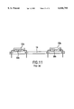
- the CCD packages 53a and 53b and the CCD holding member 54 are composed of plastics as shown in FIG. 11, when the CCD packages 53a and 53b are adhered and joined to the CCD-holding member 54, the direct transmission of heat from CCD chips 58a and 58b may cause the CCD-holding member to expand noticeably.
- all members are formed of plastics. Since, however, conventional CCD packages 53a and 53b made of plastics such as those shown in FIG. 11 are normally manufactured by injection-molding an acrylic martial, they are subjected to variation in sizes and internal condensation caused by moisture absorption.
- the conventional techniques still have many practical problems.
- the invention in the first aspect relates to a distance-measuring instrument comprising image pickup means consisting of a pair of image-forming lenses and photo sensor arrays; and arithmetic means using two images of a measured object photographed by the image pickup means to calculate the distance to the object based on the principle of triangulation.
- the image-forming lenses, a holding member for the image-forming lenses, and a holding member for the photo sensor arrays are formed of the same material, which is plastics without hygroscopicity.
- the invention in the second aspect is based on the distance-measuring instrument in the first aspect, wherein a coupling member that couples together the holding member for the image-forming lenses and the holding member for the photo sensor arrays is formed of the same material as the above material.
- the plastics without hygroscopicity are desirably an amorphous cycloolefin polymer.
- the invention in the fourth aspect provides the distance-measuring instrument in the first to third aspects, wherein members formed of the same material are joined together by deposition or melt-adhesion with an organic solvent.
- the invention in the fifth aspect provides the distance-measuring instrument in the first to fourth aspects, wherein the photo sensor arrays are arranged in such a way that the image-forming lenses, the holding member for the photo sensor arrays, and the photo sensor arrays are placed in that order along the path that the light travels.
- FIG. 1 is an explanatory sectional view of a first embodiment of the invention
- FIGS. 2(a) and 2(b) are explanatory views showing the operation of the first embodiment
- FIG. 3 is an explanatory sectional view depicting inconveniences caused by heat generated by a CCD circuit board
- FIG. 4 is an explanatory sectional view showing an improved CCD mounting structure according to the first embodiment
- FIG. 5 is an explanatory sectional view of a second embodiment of the invention.
- FIGS. 6(a)-6(e) are explanatory sectional views showing examples of a third embodiment of the invention.
- FIGS. 7(a)-7(d) are explanatory sectional views showing examples of a fourth embodiment of the invention.
- FIG. 8 is an explanatory view showing the principle of triangulation
- FIG. 9 is an explanatory sectional view of a conventional distance-measuring instrument.
- FIGS. 10(a) and 10(b) are explanatory sectional views showing the effects of differences in locations at which the CCDs are adhered.
- FIG. 11 is an explanatory sectional view showing an arrangement of conventional CCD packages.
- FIG. 1 is a vertical sectional view of the first embodiment.
- the illustration and description of arithmetic means for calculating the distance to a measured object based on the principle of triangulation are omitted.
- a pair of image-forming lenses 1a and 1b is fixed to a lens-holding member (hereafter referred to as a "frame") in such a way as to be spaced by a base length (a predetermined inter-optical-axis distance), and a pair of CCD packages 3a and 3b acting as photo sensor arrays is similarly fixed to a CCD-holding member (hereafter referred to as a "plate”) in such a way as to be spaced by a base length.
- Reference numerals 8a and 8b designate CCD chips.
- the frame 2 and the plate 4 are secured together by pouring a solvent into solvent casting ports 9.
- the frame 52 and plate 54 in FIG. 9 are composed by an aluminum die cast, and the CCD packages 53a and 53b in the same figure are formed of ceramics.
- the frame 2, the plate 4, and the CCD packages 3a and 3b are all composed of plastics (amorphous cycloolefin polymer (COP)) that constitute the image-forming lenses 1a and 1b.
- COP amorphous cycloolefin polymer
- the image-forming lenses 1a and 1b are transparent, whereas the frame 2, the plate 4, and the CCD packages 3a and 3b are black, and these components are formed of the same material.
- the components can be joined together by using an organic solvent, such as toluene, without using adhesives.
- Melt-adhesion is advantageous in that the surfaces of the plastics are melted by the solvent and after the solvent has evaporated, the molecules are firmly bonded together to provide an integral plastic material.
- this embodiment does not require complicated assembly processes such as application of the adhesives, UV temporary fixation and thermosetting, thereby substantially reducing manufacturing costs.
- amorphous cycloolefin polymer has almost no moisture absorption as compared to an acrylic material, the image-forming lenses 1a and 1b, the frame 2, the plate 4 and the CCD packages 3a and 3b are precluded from variation in size caused by moisture absorption, thereby eliminating difference in the base length between the image-forming lenses and the base length between the CCDs.
- the image-forming lenses 1a and 1b, the frame 2, the plate 4, and the CCD packages 3a and 3b may be formed of different materials as long as the base length between the image-forming lenses and the base length between the CCDs vary at the same rate. In practice, however, it is difficult to find different types of materials that meet such requirements. Thus, the same material is optimally used by taking into account the advantages obtained by the deposition or melt-joining between the components.
- FIG. 2 shows the operation of the embodiment.
- Equation 1 the distance L to the measured object is given by Equation 1 (see FIG. 2(a)).
- FIG. 2(b) shows the thermal expansion of the entire module constituting the image pickup means.
- the accuracy in the distance measurement is not affected as long as the entire module is composed of the same material (plastic) and as long as heat is uniformly transmitted.
- the CCD circuit board 10 is soldered to the CCD packages 3a and 3b. Since the CCD circuit board 10 is a printed circuit board on which CCDs and CPUs are mounted via cables to deliver signals, electronic parts, such as D/D converters, located on the CCD circuit board are expected to be heated.
- the plate 4 is elongated by thermal expansion but heat is not transmitted to the frame 2.
- the difference in temperature between the plate 4 and the frame 2 results in a different elongation percentage.
- the base length between the image-forming lens 1a and 1b differs from that between the CCD packages 3a and 3b, thereby slightly reducing the distance measuring accuracy until the entire module reaches a constant temperature.
- the CCD packages 3a and 3b are joined with the plate 4 from the rear such that the image-forming lenses 1a and 1b, the plate 4 and the CCD packages 3a and 3b are arranged in this order from the direction of light incidence, and the plate 4 is spaced from the CCD circuit board 10 to prevent heat from the electronic parts on the CCD circuit board 10 from reaching the plate 4.
- FIG. 5 is a sectional view of a second embodiment.
- the second embodiment has a structure in which the CCD chips 8a and 8b are directly mounted on the plate 4, thereby reducing the number of parts and assembly steps required for the CCD packages.
- the plate 3 has lead frames 11, and die pads (not shown) located under the shaded part (thermosetting adhesive) under the CCD chips 8a, 8b.
- the die pads serve to adhere the CCD chips 8a and 8b to the plate smoothly.
- gel (not shown), which is filled so as to cover the wires 12, can be placed over the wires to protect them from dust and moisture.
- the gel covers the wires 12 and protects them from direct contact with air.
- heat from the CCD chips 8a and 8b can be released from the rear by insulating materials 13 imbedded in the plate 4.
- FIGS. 6(a)-6(e) are sectional views of a third embodiment.
- the third embodiment is obtained by changing the combination of the structures in the enclosure of the frame/plate according to the first embodiment, and is designed for easiness in assembly and in making design changes so as to meet different specifications, and reduction in cost and size.
- the structures according to the first and second embodiments are inverted.
- This inverted type makes it simple to adjust jigs in the optical-axis adjustment mechanism for the image-forming lenses and CCDs and helps improving accurate positioning when assembling these jigs.
- CCD packages 3a and 3b are mounted on the printed circuit board (not shown) and the optical axes are adjusted while viewing output signals from the CCDs, assembly can be achieved without being affected by noise or stress, especially by installing the plate 15 for the image-forming lenses 1a and 1b that have no electronics on a rotary stage for the adjustment jigs. The accuracy in assembly also increases.
- Reference numeral 16 designates a plate.
- the frame and the plate are integrated together to form a frame/plate section 19, thereby reducing costs and the number of required parts.
- the optical systems are separated by using independent frame/plate sections 20 and 21. This separated type is suitable for miniaturization.
- the space between the right and left optical systems is not required as long as the components of the right and left optical systems and their locational relationship are accurate.
- This structure includes a lens/frame section 22 in which the image-forming lenses 1a and 1b and the frame are integrally formed.
- one member can be divided into a transparent portion, i.e. image-forming lenses 1a and 1b, and a black portion, i.e. frame.
- FIGS. 7(a)-7(d) the structure used in a fourth embodiment shown in FIGS. 7(a)-7(d) may be employed.
- FIGS. 7(a)-7(d) the top portions of the CCD packages 3a and 3b are fixed to the plate 4 as shown in FIGS. 1 and 4, but the illustration of the plate 4 is omitted for convenience.
- leads 31 from the CCD packages 3a and 3b are directly soldered to the CCD circuit boards 10a and 10b, respectively, and these circuit boards 10a and 10b are connected together at an appropriate interval by using a flexible substrate 41.
- the interval between the CCD circuit boards 10a and 10b can absorb the increase and decrease in size of each component caused by the difference in linear expansion coefficient between the CCD packages 3a and 3b or the plate 4a and the CCD circuit boards 10a and 10b.
- FIG. 7(b) The structure in FIG. 7(b) is an example in which the CCD circuit boards 10a and 10b are connected together by using a connector 42 instead of the flexible substrate 41.
- the structure in FIG. 7(c) is an example in which twisted wires 32 are used to mount the CCD packages 3a and 3b on a single CCD circuit board 10 as in FIG. 4.
- the flexibility of the twisted wires serves to absorb the increase and decrease in size of each component caused by the difference in linear expansion coefficient between the CCD packages 3a and 3b or the plate 4a and the CCD circuit board 10.
- the twisted wires 32 may be used for only the CCD package 3b, as shown in FIG. 7(d).
- the image pickup means and its holding means are made of the same plastic material without hygroscopicity, all the components are expanded and elongated under heat equally without thermal stress, and are precluded from changes in size caused by moisture absorption, thereby preventing the distance measuring accuracy from being affected.
- the distance measuring accuracy can be maintained at an almost constant level despite variations in temperature or humidity.
- this invention has the advantages: (1) costs can be reduced due to the use of a material suitable for mass production by injection molding; and (2) the device is not affected by vibration and impact due to its small weight.
- various enclosure structures can be employed.
- amorphous cycloolefin polymer having low water absorption (0.01 or lower) as the plastic as disclosed in the third aspect By using an amorphous cycloolefin polymer having low water absorption (0.01 or lower) as the plastic as disclosed in the third aspect, almost no optical or structural variation or change is caused by humidity, thereby enabling high distance measuring accuracy to be maintained in all temperature and humidity ranges. At the same time, amorphous cycloolefin polymer is excellent in heat resistance and transparency.
- the members are mutually deposited by using an organic solvent to reduce the number of required assembly steps and thus to lower the manufacturing costs.
- the photosensor arrays can be located on the rear side of the holding member so as to be separated from the circuit board for mounting. This prevents the heat source on the circuit board from affecting the photosensor arrays or the image-forming lenses. As a result, a very accurate distance-measuring instrument can be formed.
Landscapes
- Physics & Mathematics (AREA)
- Electromagnetism (AREA)
- Engineering & Computer Science (AREA)
- General Physics & Mathematics (AREA)
- Radar, Positioning & Navigation (AREA)
- Remote Sensing (AREA)
- Measurement Of Optical Distance (AREA)
- Lens Barrels (AREA)
Applications Claiming Priority (4)
| Application Number | Priority Date | Filing Date | Title |
|---|---|---|---|
| JP10-014719 | 1998-01-28 | ||
| JP1471998 | 1998-01-28 | ||
| JP10-204584 | 1998-07-21 | ||
| JP10204584A JPH11281351A (ja) | 1998-01-28 | 1998-07-21 | 測距装置 |
Publications (1)
| Publication Number | Publication Date |
|---|---|
| US6046795A true US6046795A (en) | 2000-04-04 |
Family
ID=26350732
Family Applications (1)
| Application Number | Title | Priority Date | Filing Date |
|---|---|---|---|
| US09/195,045 Expired - Fee Related US6046795A (en) | 1998-01-28 | 1998-11-19 | Distance measuring instrument |
Country Status (4)
| Country | Link |
|---|---|
| US (1) | US6046795A (de) |
| JP (1) | JPH11281351A (de) |
| KR (1) | KR100538900B1 (de) |
| DE (1) | DE19902523A1 (de) |
Cited By (21)
| Publication number | Priority date | Publication date | Assignee | Title |
|---|---|---|---|---|
| US6337736B1 (en) * | 1999-07-23 | 2002-01-08 | Fuji Electric Co., Ltd. | Thermal deformation compensating range finder |
| US20020075450A1 (en) * | 2000-11-30 | 2002-06-20 | Michiharu Aratani | Compound eye imaging system, imaging device, and electronic equipment |
| US6583433B2 (en) * | 2000-10-27 | 2003-06-24 | Fuji Electric Co., Ltd. | Range finder structure allowing easier filling of the transparent filler |
| US20030173500A1 (en) * | 2000-10-27 | 2003-09-18 | Fuji Electric Co., Ltd. | Semiconductor device module |
| US20040061848A1 (en) * | 2002-08-08 | 2004-04-01 | Shiroshi Kanemitsu | Angle detecting apparatus and projector having the same |
| US20060071151A1 (en) * | 2004-10-06 | 2006-04-06 | Fuji Electric Device Technology Co., Ltd. | Semiconductor optical sensor device and range finding method using the same |
| US20080192256A1 (en) * | 2005-09-05 | 2008-08-14 | Peter Wolf | Electro-Optical Measuring Device |
| US20080231720A1 (en) * | 2007-03-21 | 2008-09-25 | Hon Hai Precision Industry Co., Ltd. | Range finder system and electronic system having same |
| US20080231828A1 (en) * | 2005-07-28 | 2008-09-25 | Uwe Skultety Betz | Distance Measuring Equipment, and Method of Mounting an Electrooptical Unit on a Lead Frame Unit |
| US20100053414A1 (en) * | 2008-01-11 | 2010-03-04 | Satoshi Tamaki | Compound eye camera module |
| US20100118291A1 (en) * | 2008-02-18 | 2010-05-13 | Katsumi Imada | Rangefinder and range finding method |
| CN101329813B (zh) * | 2007-06-20 | 2010-09-29 | 鸿富锦精密工业(深圳)有限公司 | 三维遥控装置以及三维遥控系统 |
| US20110310290A1 (en) * | 2010-06-22 | 2011-12-22 | Shigeru Oouchida | Range-finding device and imaging apparatus |
| US20130144393A1 (en) * | 2009-12-14 | 2013-06-06 | Austin W. Mutchler | Shoulder prosthesis glenoid component |
| CN103344213A (zh) * | 2013-06-28 | 2013-10-09 | 三星电子(中国)研发中心 | 一种双摄像头测量距离的方法和装置 |
| US8780330B2 (en) | 2011-06-29 | 2014-07-15 | Sharp Kabushiki Kaisha | Optical distance-measuring device and electronic device |
| US9086480B2 (en) | 2011-06-29 | 2015-07-21 | Sharp Kabushiki Kaisha | Optical distance-measuring device and electronic device |
| US9429423B2 (en) | 2010-12-28 | 2016-08-30 | Ricoh Company, Ltd. | Ranging apparatus |
| US9568596B2 (en) | 2012-07-24 | 2017-02-14 | Sharp Kabushiki Kaisha | Optical distance measuring apparatus and electronic apparatus |
| WO2019134513A1 (zh) * | 2018-01-05 | 2019-07-11 | Oppo广东移动通信有限公司 | 拍照对焦方法、装置、存储介质及电子设备 |
| CN110389330A (zh) * | 2018-04-19 | 2019-10-29 | 莱卡地球系统公开股份有限公司 | 激光测距仪 |
Families Citing this family (5)
| Publication number | Priority date | Publication date | Assignee | Title |
|---|---|---|---|---|
| JP3958115B2 (ja) * | 2002-05-28 | 2007-08-15 | ナイルス株式会社 | 回転検出装置 |
| DE102004001425A1 (de) * | 2004-01-09 | 2005-08-04 | Robert Bosch Gmbh | Optische Sensorvorrichtung mit zumindest teilweise in das Gerätegehäuse integrierter Optik |
| JP4691508B2 (ja) | 2004-11-15 | 2011-06-01 | 日立オートモティブシステムズ株式会社 | ステレオカメラ |
| JP2007119660A (ja) * | 2005-10-31 | 2007-05-17 | Nippon Zeon Co Ltd | 環状オレフィン付加共重合体、その製造方法、及び成形用材料 |
| JP2008124923A (ja) * | 2006-11-14 | 2008-05-29 | Matsushita Electric Works Ltd | カメラモジュール |
Citations (10)
| Publication number | Priority date | Publication date | Assignee | Title |
|---|---|---|---|---|
| US4313654A (en) * | 1977-09-06 | 1982-02-02 | Minolta Camera Kabushiki Kaisha | Automatic rangefinder system for photographic camera with light emitting and receiving means |
| US4529287A (en) * | 1983-08-09 | 1985-07-16 | Minolta Camera Kabushiki Kaisha | Focus condition detection device for cameras |
| US4662735A (en) * | 1985-01-16 | 1987-05-05 | Minolta Camera Kabushiki Kaisha | Plastic lens elements supporting structure |
| JPS63253317A (ja) * | 1987-04-10 | 1988-10-20 | Hitachi Ltd | レンズ鏡胴 |
| US5233382A (en) * | 1991-04-03 | 1993-08-03 | Fuji Photo Film Company, Ltd. | Range finding device unaffected by environmental conditions |
| JPH08267585A (ja) * | 1995-03-31 | 1996-10-15 | Toray Ind Inc | 溶着樹脂成形品およびその製造方法 |
| JPH0996524A (ja) * | 1995-10-02 | 1997-04-08 | Fuji Electric Co Ltd | 測距装置 |
| JPH09176223A (ja) * | 1995-12-13 | 1997-07-08 | Hoechst Ag | シクロオレフィンコポリマーを調製する方法 |
| US5721994A (en) * | 1994-04-15 | 1998-02-24 | Olympus Optical Co., Ltd. | Photographing apparatus for recording data on films |
| US5745805A (en) * | 1993-05-14 | 1998-04-28 | Olympus Optical Co., Ltd. | Focus detecting device |
Family Cites Families (4)
| Publication number | Priority date | Publication date | Assignee | Title |
|---|---|---|---|---|
| JPS58199303A (ja) * | 1982-05-17 | 1983-11-19 | Takashi Mori | 太陽光収集装置 |
| JPS63177104A (ja) * | 1987-01-19 | 1988-07-21 | Hitachi Ltd | プラスチツクレンズ鏡筒 |
| JPH0968839A (ja) * | 1995-09-01 | 1997-03-11 | Konica Corp | カラー画像形成装置 |
| JPH10177103A (ja) * | 1996-12-18 | 1998-06-30 | Dainippon Printing Co Ltd | マイクロレンズ構体 |
-
1998
- 1998-07-21 JP JP10204584A patent/JPH11281351A/ja not_active Withdrawn
- 1998-11-19 US US09/195,045 patent/US6046795A/en not_active Expired - Fee Related
-
1999
- 1999-01-22 DE DE19902523A patent/DE19902523A1/de not_active Ceased
- 1999-01-26 KR KR10-1999-0002345A patent/KR100538900B1/ko not_active IP Right Cessation
Patent Citations (10)
| Publication number | Priority date | Publication date | Assignee | Title |
|---|---|---|---|---|
| US4313654A (en) * | 1977-09-06 | 1982-02-02 | Minolta Camera Kabushiki Kaisha | Automatic rangefinder system for photographic camera with light emitting and receiving means |
| US4529287A (en) * | 1983-08-09 | 1985-07-16 | Minolta Camera Kabushiki Kaisha | Focus condition detection device for cameras |
| US4662735A (en) * | 1985-01-16 | 1987-05-05 | Minolta Camera Kabushiki Kaisha | Plastic lens elements supporting structure |
| JPS63253317A (ja) * | 1987-04-10 | 1988-10-20 | Hitachi Ltd | レンズ鏡胴 |
| US5233382A (en) * | 1991-04-03 | 1993-08-03 | Fuji Photo Film Company, Ltd. | Range finding device unaffected by environmental conditions |
| US5745805A (en) * | 1993-05-14 | 1998-04-28 | Olympus Optical Co., Ltd. | Focus detecting device |
| US5721994A (en) * | 1994-04-15 | 1998-02-24 | Olympus Optical Co., Ltd. | Photographing apparatus for recording data on films |
| JPH08267585A (ja) * | 1995-03-31 | 1996-10-15 | Toray Ind Inc | 溶着樹脂成形品およびその製造方法 |
| JPH0996524A (ja) * | 1995-10-02 | 1997-04-08 | Fuji Electric Co Ltd | 測距装置 |
| JPH09176223A (ja) * | 1995-12-13 | 1997-07-08 | Hoechst Ag | シクロオレフィンコポリマーを調製する方法 |
Cited By (27)
| Publication number | Priority date | Publication date | Assignee | Title |
|---|---|---|---|---|
| US6337736B1 (en) * | 1999-07-23 | 2002-01-08 | Fuji Electric Co., Ltd. | Thermal deformation compensating range finder |
| US6583433B2 (en) * | 2000-10-27 | 2003-06-24 | Fuji Electric Co., Ltd. | Range finder structure allowing easier filling of the transparent filler |
| US20030173500A1 (en) * | 2000-10-27 | 2003-09-18 | Fuji Electric Co., Ltd. | Semiconductor device module |
| US6906316B2 (en) | 2000-10-27 | 2005-06-14 | Fuji Electric Co., Ltd. | Semiconductor device module |
| US20020075450A1 (en) * | 2000-11-30 | 2002-06-20 | Michiharu Aratani | Compound eye imaging system, imaging device, and electronic equipment |
| US7042560B2 (en) * | 2002-08-08 | 2006-05-09 | Seiko Precision Inc. | Angle detecting apparatus and projector having the same |
| US20040061848A1 (en) * | 2002-08-08 | 2004-04-01 | Shiroshi Kanemitsu | Angle detecting apparatus and projector having the same |
| US20060071151A1 (en) * | 2004-10-06 | 2006-04-06 | Fuji Electric Device Technology Co., Ltd. | Semiconductor optical sensor device and range finding method using the same |
| US20080231828A1 (en) * | 2005-07-28 | 2008-09-25 | Uwe Skultety Betz | Distance Measuring Equipment, and Method of Mounting an Electrooptical Unit on a Lead Frame Unit |
| US20080192256A1 (en) * | 2005-09-05 | 2008-08-14 | Peter Wolf | Electro-Optical Measuring Device |
| US7796250B2 (en) | 2005-09-05 | 2010-09-14 | Robert Bosch Gmbh | Electro-optical measuring device |
| US20080231720A1 (en) * | 2007-03-21 | 2008-09-25 | Hon Hai Precision Industry Co., Ltd. | Range finder system and electronic system having same |
| US7583363B2 (en) * | 2007-03-21 | 2009-09-01 | Hon Hai Precision Industry Co., Ltd. | Range finder system and electronic system having same |
| CN101329813B (zh) * | 2007-06-20 | 2010-09-29 | 鸿富锦精密工业(深圳)有限公司 | 三维遥控装置以及三维遥控系统 |
| US20100053414A1 (en) * | 2008-01-11 | 2010-03-04 | Satoshi Tamaki | Compound eye camera module |
| US20100118291A1 (en) * | 2008-02-18 | 2010-05-13 | Katsumi Imada | Rangefinder and range finding method |
| US7924409B2 (en) * | 2008-02-18 | 2011-04-12 | Panasonic Corporation | Rangefinder and range finding method |
| US20130144393A1 (en) * | 2009-12-14 | 2013-06-06 | Austin W. Mutchler | Shoulder prosthesis glenoid component |
| US20110310290A1 (en) * | 2010-06-22 | 2011-12-22 | Shigeru Oouchida | Range-finding device and imaging apparatus |
| US9267797B2 (en) * | 2010-06-22 | 2016-02-23 | Ricoh Company, Ltd. | Range-finding device and imaging apparatus |
| US9429423B2 (en) | 2010-12-28 | 2016-08-30 | Ricoh Company, Ltd. | Ranging apparatus |
| US8780330B2 (en) | 2011-06-29 | 2014-07-15 | Sharp Kabushiki Kaisha | Optical distance-measuring device and electronic device |
| US9086480B2 (en) | 2011-06-29 | 2015-07-21 | Sharp Kabushiki Kaisha | Optical distance-measuring device and electronic device |
| US9568596B2 (en) | 2012-07-24 | 2017-02-14 | Sharp Kabushiki Kaisha | Optical distance measuring apparatus and electronic apparatus |
| CN103344213A (zh) * | 2013-06-28 | 2013-10-09 | 三星电子(中国)研发中心 | 一种双摄像头测量距离的方法和装置 |
| WO2019134513A1 (zh) * | 2018-01-05 | 2019-07-11 | Oppo广东移动通信有限公司 | 拍照对焦方法、装置、存储介质及电子设备 |
| CN110389330A (zh) * | 2018-04-19 | 2019-10-29 | 莱卡地球系统公开股份有限公司 | 激光测距仪 |
Also Published As
| Publication number | Publication date |
|---|---|
| KR19990068122A (ko) | 1999-08-25 |
| KR100538900B1 (ko) | 2005-12-27 |
| DE19902523A1 (de) | 1999-07-29 |
| JPH11281351A (ja) | 1999-10-15 |
Similar Documents
| Publication | Publication Date | Title |
|---|---|---|
| US6046795A (en) | Distance measuring instrument | |
| US11627239B2 (en) | Photosensitive assembly and camera module and manufacturing method thereof | |
| US11223751B2 (en) | Photosensitive assembly and camera module and manufacturing method thereof | |
| US7046344B2 (en) | Range finder | |
| JP5601000B2 (ja) | 撮像装置 | |
| US6384397B1 (en) | Low cost die sized module for imaging application having a lens housing assembly | |
| JP3738824B2 (ja) | 光学装置及びその製造方法並びに電子機器 | |
| US5068713A (en) | Solid state image sensing device | |
| US5233382A (en) | Range finding device unaffected by environmental conditions | |
| US20060071151A1 (en) | Semiconductor optical sensor device and range finding method using the same | |
| JP2002252796A (ja) | 撮像装置 | |
| US5949062A (en) | Image sensor secured to a frame | |
| US7829833B2 (en) | Arranging and/or supporting an image pickup device in an image pickup apparatus | |
| US6414299B1 (en) | Method of mounting optical sensor package | |
| US7670064B2 (en) | Optical module and optical system | |
| US5801374A (en) | Precision optical sensor packaging | |
| JP3503467B2 (ja) | カメラ | |
| JPH10239050A (ja) | 測距装置 | |
| JP2880821B2 (ja) | 測距用光学モジュール | |
| JP7078151B2 (ja) | 撮像ユニットおよび撮像装置 | |
| JPH10281761A (ja) | 測距装置 | |
| JP4467656B2 (ja) | 焦点検出装置及び位置調整方法 | |
| JPH07114291B2 (ja) | 光学センサ素子 | |
| JP6849016B2 (ja) | 撮像ユニットおよび撮像装置 | |
| JP6547799B2 (ja) | 撮像ユニットおよび撮像装置 |
Legal Events
| Date | Code | Title | Description |
|---|---|---|---|
| AS | Assignment |
Owner name: FUJI ELECTRONIC CO., LTD., JAPAN Free format text: ASSIGNMENT OF ASSIGNORS INTEREST;ASSIGNORS:SUGIYAMA, OSAMU;HIRATA, NOBUO;FUKAMURA, HAJIME;AND OTHERS;REEL/FRAME:009688/0477 Effective date: 19981218 |
|
| FEPP | Fee payment procedure |
Free format text: PAYOR NUMBER ASSIGNED (ORIGINAL EVENT CODE: ASPN); ENTITY STATUS OF PATENT OWNER: LARGE ENTITY |
|
| FPAY | Fee payment |
Year of fee payment: 4 |
|
| FPAY | Fee payment |
Year of fee payment: 8 |
|
| REMI | Maintenance fee reminder mailed | ||
| LAPS | Lapse for failure to pay maintenance fees | ||
| LAPS | Lapse for failure to pay maintenance fees |
Free format text: PATENT EXPIRED FOR FAILURE TO PAY MAINTENANCE FEES (ORIGINAL EVENT CODE: EXP.); ENTITY STATUS OF PATENT OWNER: LARGE ENTITY |
|
| STCH | Information on status: patent discontinuation |
Free format text: PATENT EXPIRED DUE TO NONPAYMENT OF MAINTENANCE FEES UNDER 37 CFR 1.362 |
|
| FP | Lapsed due to failure to pay maintenance fee |
Effective date: 20120404 |