US5805232A - Vertical sync signal separator circuit and multi-sync monitor using the same - Google Patents
Vertical sync signal separator circuit and multi-sync monitor using the same Download PDFInfo
- Publication number
- US5805232A US5805232A US08/753,017 US75301796A US5805232A US 5805232 A US5805232 A US 5805232A US 75301796 A US75301796 A US 75301796A US 5805232 A US5805232 A US 5805232A
- Authority
- US
- United States
- Prior art keywords
- sync signal
- circuit
- voltage
- capacitor
- vertical sync
- Prior art date
- Legal status (The legal status is an assumption and is not a legal conclusion. Google has not performed a legal analysis and makes no representation as to the accuracy of the status listed.)
- Expired - Fee Related
Links
Images


Classifications
-
- G—PHYSICS
- G06—COMPUTING OR CALCULATING; COUNTING
- G06F—ELECTRIC DIGITAL DATA PROCESSING
- G06F3/00—Input arrangements for transferring data to be processed into a form capable of being handled by the computer; Output arrangements for transferring data from processing unit to output unit, e.g. interface arrangements
- G06F3/14—Digital output to display device ; Cooperation and interconnection of the display device with other functional units
-
- H—ELECTRICITY
- H04—ELECTRIC COMMUNICATION TECHNIQUE
- H04N—PICTORIAL COMMUNICATION, e.g. TELEVISION
- H04N5/00—Details of television systems
- H04N5/04—Synchronising
- H04N5/08—Separation of synchronising signals from picture signals
- H04N5/10—Separation of line synchronising signal from frame synchronising signal or vice versa
Definitions
- the present invention relates to a vertical sync signal separator and a multi-sync monitor using the same and, particularly, to a vertical sync separator of a multi-sync monitor for separating, among others, a vertical sync signal from a composite video signal sent from a personal computer to a multi-sync monitor such as a multi-sync CRT display, which is capable of responding to wide horizontal and vertical sync frequency ranges and of more reliably separating the vertical sync signal in a wide frequency range.
- a personal computer can selectively set the number of vertical and/or horizontal scan lines of a CRT display according to one of various software including Windows (registered trademark).
- a high definition multi-sync CRT to be connected to such a personal computer may have a number of horizontal dots of 1200 or more and a number of vertical dots, that is, the number of vertical scan lines, of 800 or more, corresponding to the number of horizontal dots.
- a vertical sync separator circuit receives a composite sync signal including a horizontal sync signal having high frequency, a vertical sync signal thereof which is to be separated takes the form of a pulse signal having a pulse width narrower than that of the horizontal sync signal of a conventional TV signal.
- FIG. 3 shows an example of a vertical sync signal separator contained in a conventional multi-sync CRT.
- the vertical sync signal separator has an input terminal 1a and an output terminal 1b.
- the vertical sync separator comprises a sync signal separator circuit 1, a vertical sync signal separator circuit 2 and a phase detector circuit 3.
- the sync signal separator circuit 1 receives a composite video signal supplied from a personal computer to the input terminal 1a.
- the sync signal separator circuit 1 separates a composite sync signal containing a vertical sync signal and a horizontal sync signal from the composite video signal and supplies the composite sync signal to the vertical sync separator circuit 2.
- the vertical sync separator circuit 2 separates the vertical sync signal from the composite sync signal and supplies it to the output terminal 1b.
- the composite sync signal separated from the composite video signal by the sync signal separator circuit 1 contains a horizontal equalizing pulse in a vertical blanking period and is supplied to the phase detector circuit 3 and a horizontal sync signal detector circuit which is not shown as a signal containing a horizontal sync signal.
- the vertical sync signal separator circuit 2 comprises an integration circuit 4 for receiving the composite sync signal and a comparator 5 connected to an output of the integration circuit 4.
- the integration circuit 4 includes a resistor R1 and a capacitor C1.
- the comparator 5 has a (-) input supplied with a reference voltage from a reference voltage source 6 and a (+) input supplied with an integrated voltage value from the integration circuit 4.
- the vertical sync signal is detected by detecting a voltage having a value larger than that of the horizontal sync signal during the vertical sync signal period and generated by integrating by the integration circuit 4 the vertical sync signal under a condition that the pulse width of the vertical sync signal is larger than that of the horizontal sync signal.
- the pulse width of the vertical sync signal is reduced with increase of the horizontal sync signal frequency.
- the pulse width of 1 pulse (1 H) of the horizontal sync signal is 20 ⁇ s and that of 1 pulse (1V syn ) of the vertical sync signal is 46.7 ⁇ s at the horizontal sync signal frequency of 15 kHz.
- 1 H is about 3.75 ⁇ s and 1V syn is about 8.75 ⁇ s.
- 1 H is about 1.5 ⁇ s and 1V syn is about 3.5 ⁇ s.
- the pulse width of the vertical sync signal when a high horizontal sync signal frequency is received is narrower than that of the horizontal sync signal when a low horizontal sync signal frequency is received. Consequently, it becomes impossible to separate the vertical sync signal from the composite sync signal.
- An object of the present invention is to provide a vertical sync signal separator circuit capable of reliably separating a vertical sync signal from a composite sync signal including a horizontal sync signal having frequency in a wide frequency range and a multi-sync monitor using the same vertical sync signal separator.
- a multi-sync monitor according to the present invention comprises the vertical sync signal separator.
- the charging current which increases with increase of the horizontal sync signal frequency is supplied to the capacitor so that a charging voltage compatible with a charging voltage for a low horizontal sync signal frequency is generated thereacross even if the pulse width of the horizontal sync signal as well as the vertical sync signal is reduced, to thereby restrict a variation of the charging voltage due to difference in the horizontal sync signal frequency.
- the vertical sync signal is detected when the comparator determines that the pulse width of the vertical sync signal is larger than that of the horizontal sync signal, as in the conventional manner.
- the charge/discharge circuit comprises a one-shot circuit responsive to the vertical sync signal and the horizontal sync signal of the composite sync signal to generate a pulse voltage having a predetermined pulse width and an integrator circuit for integrating the pulses output from the one-shot circuit to generate a predetermined DC voltage signal.
- the DC voltage signal is converted into a current with which the capacitor is charged.
- the capacitor is discharged when there is no vertical and horizontal sync signals received by the charge/discharge circuit.
- the one-shot circuit generates the pulse signal having a constant pulse width corresponding to the composite sync signal, regardless of the horizontal sync signal frequency of the composite sync signal.
- the pulse signal from the one-shot circuit which has the constant pulse width in only a period of the horizontal sync signal of the composite sync signal, is integrated by the integrator circuit, resulting in the DC voltage signal corresponding to the horizontal sync signal frequency.
- the capacitor is charged with a current value corresponding to a voltage value of the DC voltage signal. Therefore, although a charging time becomes short when the horizontal sync signal frequency is high, the capacitor is charged with a large charging current by increasing the voltage value of the DC voltage signal, resulting in a high charge voltage of the capacitor. On the contrary, although the charging time becomes long when the horizontal sync signal frequency is low, the capacitor is charged with a small charging current by reducing the voltage value of the DC voltage, resulting in a high charge voltage of the capacitor.
- the difference in charge voltage of the capacitor in the time period of the vertical and horizontal sync signals of the composite sync signal which is caused by the difference in horizontal sync signal frequency, is eventually cancelled out.
- the duty cycle of the horizontal sync signal at any frequency is 50% or less under current TV standards in major countries and the duty cycle of the vertical sync signal is 50% or more. Therefore, a peak value of the vertical sync signal is higher than that of the horizontal sync signal for any horizontal sync signal frequency.
- the reference value in such case is set to a value which is larger than the peak value of the charge/discharge voltage value generated in the period of the horizontal sync signal and smaller than the peak value of the charge/discharge voltage value generated in the period of the vertical sync signal.
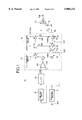
- FIG. 1 is a block circuit diagram according to an embodiment of a vertical sync signal separator of the present invention
- FIG. 2 shows waveforms for explaining an operation of the embodiment shown in FIG. 1;
- FIG. 3 is a circuit diagram of a conventional sync signal separator circuit having a vertical sync signal separator circuit.
- a vertical sync signal separator circuit 10 comprises an inverter/amplifier 11, a one-shot circuit 12, a low-pass filter (LPF) 13, a voltage/current (V/I) converter circuit 14, a charge/discharge circuit 15, a charging capacitor (C) 16 and a hysterisis comparator (COM) 17.
- the inverter/amplifier 11 has an input terminal 10a supplied with a composite sync signal containing a vertical and horizontal sync signals from a sync signal separator circuit 1 shown in FIG. 3, inverts/amplifies the composite sync signal and outputs a positive pulse signal such as shown by (a) in FIG. 2.
- the one-shot circuit 12 is triggered by a leading edge of the output pulse from the inverter/amplifier 11 to generate a pulse having a predetermined pulse width W in a period corresponding to the sync signal.
- the pulse width W of the output of the one-shot circuit 12 is determined with using, as a reference, a period T which is determined by a maximum horizontal frequency which can be received by a multi-sync CRT housing the sync signal separator 10 as a frequency of the horizontal sync signal.
- the width W may be set to be equal to or more than a duty factor of the vertical sync signal V P (see FIG. 2). For example, when the duty factor of the vertical sync signal V P is 70%, the pulse width W may be set to have a duty factor of 80%.
- the pulse width thereof is further increased although the value of the DC voltage becomes smaller. Therefore, it is possible to supply the charging voltage having high peak value to the capacitor 16 similarly even if the DC voltage value varies more or less. Since, as will be described in detail, the charging current value itself is reduced with decrease of the horizontal sync signal frequency, the peak value of the charging voltage for the vertical sync signal is not changed substantially practically even if the horizontal sync signal frequency is changed.
- the duty factor of the horizontal sync signal is 50% at most and the duty factor of the vertical sync signal is at least 50%. Therefore, the peak value of the vertical sync signal is higher than that of the horizontal sync signal for any horizontal sync signal frequency.
- the vertical sync signal V P has a pulse width of 3.5 ⁇ s, with the duty factor of 30% using the period T as the reference and the horizontal sync signal H P has a pulse width of 1.5 ⁇ s, with the duty factor of 30% using the period T as the reference.
- the low-pass filter 13 serves as an integration circuit which integrates the output pulse signal of the one-shot circuit 12 to generate a mean DC voltage shown by a dotted line V dc in FIG. 2, with the maximum horizontal sync signal frequency being 200 kHz.
- the V/I converter circuit 14 converts the voltage value V dc into a current value which is supplied to the charge/discharge circuit 15.
- the V/I converter circuit 14 comprises a buffer amplifier 141 composed of a differential amplifier having an input terminal connected to the output terminal of the low-pass filter 13, an NPN transistor Q1 having a base connected to an output of the buffer amplifier 141 and a resistor R connected between an emitter of the NPN transistor Q1 and ground GND. An emitter voltage of the NPN transistor Q1.
- a NPN transistor Q2 is connected between a collector of the NPN transistor Q1 and a power source line V cc as a diode-connected load transistor.
- the transistor Q2 is used as the input side transistor constituting a current mirror circuit and has a base connected to bases of output side transistors Q3 and Q4 of the current mirror circuit, which are provided in the charge/discharge circuit 15.
- currents each substantially equal to a current flowing in the transistor Q2 flow through collector-emitter circuits of the respective transistors Q3 and Q4 and output therefrom as output currents.
- the output currents of the transistors Q3 and Q4 of the charge/discharge circuit 15 flow through respective transistors Q5 and Q6 which constitute the current mirror circuit to the ground GND.
- a junction N between the transistors Q4 and Q6 is connected to a charging side terminal of the capacitor 16 as an output of the charge/discharge circuit 15.
- the transistors Q3 to Q6 produce a charging current and a discharging current having a value equal to that of the charging current at the junction N as to be described in detail later.
- the charging current is supplied to the capacitor 16 only during a time period where the horizontal and vertical sync signals exist and the discharging current flows from the capacitor 16 to the ground GND only during a time period where there is neither the vertical sync signal nor the horizontal sync signal.
- the capacitor 16 generates a voltage waveform H s and a voltage waveform V S shown by (c) in FIG. 2 correspondingly to the horizontal sync signal H P and to the vertical sync signal V P , respectively, when the maximum horizontal sync signal frequency is 200 kHz.
- the waveforms of these voltages will be described.
- These waveforms are determined by the charging and discharging current values of the charge/discharge circuit 15 and a capacitance of the capacitor 16.
- the charging current value and the discharging current value are set by selecting a value of the resistor R connected to the emitter of the transistor Q1 of the V/I converter circuit 14. Assuming that the charge/discharge current is constant and represented by I dc , the charge/discharge current I dc becomes V dc /R, where R is the resistance value of the resistor R and V dc is an output voltage of the low-pass filter 13.
- the hysterisis comparator 17 has a high level threshold value H and a low level threshold value L as shown by the waveform (c) in FIG. 2.
- the threshold value H is in a level close to a bottom of a valley between two peaks generated in a center portion of the voltage waveform V S during the period of the vertical sync signal V P and the threshold value L corresponds to about a peak level of the horizontal sync signal H P .
- a vertical sync signal V syn shown by a waveform (d) in FIG. 2 is generated at an output terminal 10b of the comparator 17.
- the diode-connected transistor Q2 of the V/I converter circuit 14 serves as the input side load of the current mirror circuit constituted with the transistors Q3 and Q4 of the charge/discharge circuit 15.
- the output side transistors Q3 and Q4 of the current mirror circuit have emitters connected to the power source line V cc and collectors connected to the ground GND through a current mirror load 151 composed of the diode-connected NPN transistor Q5 and the NPN transistor Q6.
- An emitter area of the transistor Q6 is twice that of the transistor Q5, so that the transistor Q6 can flow a current twice that of the transistor Q5.
- a switch circuit 152 composed of an NPN transistor Q7 is connected between the collector of the transistor Q5 and the ground GND.
- the transistor Q7 has a base supplied with the sync signals corresponding to the vertical and horizontal sync signals from the inverter/amplifier 11. Further, the transistor Q7 has an emitter connected to the ground GND so that it becomes conductive state only during the period in which there is the sync signal.
- the current I dc of the transistor Q4 is supplied to the capacitor 16 as the charging current. Since the capacitor 16 is charged with the constant current I dc , the voltage of the capacitor 16 becomes a sawtooth waveform as shown by the waveform (c) in FIG. 2. Further, since the time period in which the transistor Q7 is conductive is the time period in which the sync signal exists, the charging time of the capacitor 15 becomes shorter for the horizontal sync signal H P , while the charging time of the capacitor 15, in which the vertical sync signal V P exists, is longer.
- the transistors Q5 and Q6 of the current mirror circuit 151 are in an ON state during an OFF period of the transistor Q7, a current 2 ⁇ I dc which is twice the current of the transistor Q5 flows through the transistor Q6.
- the transistor Q6 sinks the current I dc of the transistor Q4 and the current I dc of the capacitor 16 and, since the sink current becomes 2 ⁇ I dc , the discharging current of the capacitor 16 becomes I dc . That is, the discharge is started from the peak of the charging current with a discharging rate which is the same as that of the charging rate in an opposite direction to the charging direction, resulting in the voltage waveform (c) of the capacitor 16 as shown in FIG. 2.
- the output voltage V dc of the low-pass filter 13 is lowered to a level shown by a dotted line. Therefore, the charge/discharge current I dc is reduced to V dc /R. Consequently, the capacitor 16 is charged/discharged with a current which is smaller than that in the former case. In this case, the charging rate and discharging rate become lower than those in the former case as shown by the waveform (g) in FIG. 2 and the vertical and horizontal sync signals become broader in the time axis direction.
- the present circuit performs the charging/discharging by changing the charging/discharging current value corresponding to the change of the horizontal sync signal frequency. Therefore, the variation of the voltage level of the capacitor 16 can be restricted. As a result, even when a composite sync signal having a different horizontal sync signal frequency is received, it is possible to separate a vertical sync signal V syn therefrom by means of the comparator 17.
- the described charge/discharge circuit is a mere example and it is possible to realize a similar charge/discharge circuit by using NPN transistors and PNP transistors instead of the described PNP transistors and the described NPN transistors, respectively.
- the described hysterisis comparator may be changed to a comparator having one threshold value.
Landscapes
- Engineering & Computer Science (AREA)
- Multimedia (AREA)
- Signal Processing (AREA)
- Theoretical Computer Science (AREA)
- Human Computer Interaction (AREA)
- Physics & Mathematics (AREA)
- General Engineering & Computer Science (AREA)
- General Physics & Mathematics (AREA)
- Synchronizing For Television (AREA)
Applications Claiming Priority (2)
| Application Number | Priority Date | Filing Date | Title |
|---|---|---|---|
| JP7-329543 | 1995-11-24 | ||
| JP7329543A JPH09149287A (ja) | 1995-11-24 | 1995-11-24 | 垂直同期信号分離回路およびこれを有する表示装置 |
Publications (1)
| Publication Number | Publication Date |
|---|---|
| US5805232A true US5805232A (en) | 1998-09-08 |
Family
ID=18222541
Family Applications (1)
| Application Number | Title | Priority Date | Filing Date |
|---|---|---|---|
| US08/753,017 Expired - Fee Related US5805232A (en) | 1995-11-24 | 1996-11-19 | Vertical sync signal separator circuit and multi-sync monitor using the same |
Country Status (4)
| Country | Link |
|---|---|
| US (1) | US5805232A (ja) |
| JP (1) | JPH09149287A (ja) |
| KR (1) | KR100432352B1 (ja) |
| TW (1) | TW311318B (ja) |
Cited By (5)
| Publication number | Priority date | Publication date | Assignee | Title |
|---|---|---|---|---|
| US6018370A (en) * | 1997-05-08 | 2000-01-25 | Sony Corporation | Current source and threshold voltage generation method and apparatus for HHK video circuit |
| US6028640A (en) * | 1997-05-08 | 2000-02-22 | Sony Corporation | Current source and threshold voltage generation method and apparatus for HHK video circuit |
| US6424379B1 (en) * | 1999-09-08 | 2002-07-23 | Mitsubishi Denki Kabushiki Kaisha | Vertical synchronization separation circuit |
| US20030156083A1 (en) * | 2002-02-19 | 2003-08-21 | Willis Thomas E. | Sparse refresh double-buffering |
| US20070273423A1 (en) * | 2006-05-26 | 2007-11-29 | Semiconductor Components Industries, Llc | Accurate timing generator and method therefor |
Citations (6)
| Publication number | Priority date | Publication date | Assignee | Title |
|---|---|---|---|---|
| US4313137A (en) * | 1980-05-06 | 1982-01-26 | Zenith Radio Corporation | Integratable vertical sync separator |
| JPS61181276A (ja) * | 1985-02-07 | 1986-08-13 | Matsushita Electric Ind Co Ltd | 垂直同期信号増巾器 |
| JPH03233279A (ja) * | 1990-02-09 | 1991-10-17 | Matsushita Refrig Co Ltd | 除霜制御装置 |
| JPH0443769A (ja) * | 1990-06-08 | 1992-02-13 | Sanyo Electric Co Ltd | 垂直同期信号分離回路 |
| JPH04331574A (ja) * | 1991-05-07 | 1992-11-19 | Matsushita Electric Ind Co Ltd | 同期分離回路 |
| JPH0541817A (ja) * | 1991-05-22 | 1993-02-19 | Sony Corp | 垂直同期分離回路 |
-
1995
- 1995-11-24 JP JP7329543A patent/JPH09149287A/ja active Pending
-
1996
- 1996-10-23 TW TW085112972A patent/TW311318B/zh active
- 1996-11-14 KR KR1019960054014A patent/KR100432352B1/ko not_active Expired - Fee Related
- 1996-11-19 US US08/753,017 patent/US5805232A/en not_active Expired - Fee Related
Patent Citations (6)
| Publication number | Priority date | Publication date | Assignee | Title |
|---|---|---|---|---|
| US4313137A (en) * | 1980-05-06 | 1982-01-26 | Zenith Radio Corporation | Integratable vertical sync separator |
| JPS61181276A (ja) * | 1985-02-07 | 1986-08-13 | Matsushita Electric Ind Co Ltd | 垂直同期信号増巾器 |
| JPH03233279A (ja) * | 1990-02-09 | 1991-10-17 | Matsushita Refrig Co Ltd | 除霜制御装置 |
| JPH0443769A (ja) * | 1990-06-08 | 1992-02-13 | Sanyo Electric Co Ltd | 垂直同期信号分離回路 |
| JPH04331574A (ja) * | 1991-05-07 | 1992-11-19 | Matsushita Electric Ind Co Ltd | 同期分離回路 |
| JPH0541817A (ja) * | 1991-05-22 | 1993-02-19 | Sony Corp | 垂直同期分離回路 |
Cited By (7)
| Publication number | Priority date | Publication date | Assignee | Title |
|---|---|---|---|---|
| US6018370A (en) * | 1997-05-08 | 2000-01-25 | Sony Corporation | Current source and threshold voltage generation method and apparatus for HHK video circuit |
| US6028640A (en) * | 1997-05-08 | 2000-02-22 | Sony Corporation | Current source and threshold voltage generation method and apparatus for HHK video circuit |
| US6424379B1 (en) * | 1999-09-08 | 2002-07-23 | Mitsubishi Denki Kabushiki Kaisha | Vertical synchronization separation circuit |
| US20030156083A1 (en) * | 2002-02-19 | 2003-08-21 | Willis Thomas E. | Sparse refresh double-buffering |
| US20070273423A1 (en) * | 2006-05-26 | 2007-11-29 | Semiconductor Components Industries, Llc | Accurate timing generator and method therefor |
| US7579892B2 (en) * | 2006-05-26 | 2009-08-25 | Semiconductor Components Industries, L.L.C. | Accurate timing generator and method therefor |
| CN101079617B (zh) * | 2006-05-26 | 2012-07-04 | 半导体元件工业有限责任公司 | 精确的定时信号发生器及其方法 |
Also Published As
| Publication number | Publication date |
|---|---|
| KR970028998A (ko) | 1997-06-26 |
| TW311318B (ja) | 1997-07-21 |
| JPH09149287A (ja) | 1997-06-06 |
| KR100432352B1 (ko) | 2004-09-04 |
Similar Documents
| Publication | Publication Date | Title |
|---|---|---|
| JP2005151777A (ja) | チャージポンプ回路およびアンプ | |
| US4446443A (en) | Amplifier having reduced power dissipation and improved slew rate | |
| US5805232A (en) | Vertical sync signal separator circuit and multi-sync monitor using the same | |
| US7423698B2 (en) | Amplifier for amplifying input signal such as video signal and outputting amplified signal | |
| US4313137A (en) | Integratable vertical sync separator | |
| US4637066A (en) | Noise blanking signal generator for AM radio | |
| EP0148606B1 (en) | Tri-level sandcastle pulse decoder | |
| US4682087A (en) | Apparatus for controlling amplitude of vertical deflection signal | |
| US5345117A (en) | Synchronous separating circuit | |
| KR0155615B1 (ko) | 영상출력장치의 동기신호분리회로 | |
| US5689308A (en) | Vertical reset genereator circuit | |
| US5237222A (en) | Comparator circuit for an integrator | |
| JP3089021B2 (ja) | 垂直偏向用鋸歯状波発生回路 | |
| JPH06225313A (ja) | テレビジョン方式を識別する回路 | |
| US4942314A (en) | Peak holding circuit for a color television receiver | |
| JP3879148B2 (ja) | クランプ回路およびそれを用いた同期分離回路 | |
| KR100228892B1 (ko) | 수직 동기 신호 분리 회로 | |
| KR100404581B1 (ko) | 동기신호 생성회로 | |
| JPH0441660Y2 (ja) | ||
| JPS6221372A (ja) | 垂直周期信号の振幅制御回路 | |
| JP2722455B2 (ja) | ビーム電流制限回路 | |
| EP0242907A1 (en) | Coincidence circuit in a line synchronizing circuit arrangement | |
| US7554607B2 (en) | Video signal detection circuit | |
| JP3263571B2 (ja) | 映像信号処理回路 | |
| JPH04280182A (ja) | テレビジョン信号自動判別装置 |
Legal Events
| Date | Code | Title | Description |
|---|---|---|---|
| AS | Assignment |
Owner name: ROHM CO., LTD., JAPAN Free format text: ASSIGNMENT OF ASSIGNORS INTEREST;ASSIGNOR:NINOMIYA, KOSHI;REEL/FRAME:008281/0049 Effective date: 19961031 |
|
| FEPP | Fee payment procedure |
Free format text: PAYOR NUMBER ASSIGNED (ORIGINAL EVENT CODE: ASPN); ENTITY STATUS OF PATENT OWNER: LARGE ENTITY |
|
| FPAY | Fee payment |
Year of fee payment: 4 |
|
| FPAY | Fee payment |
Year of fee payment: 8 |
|
| REMI | Maintenance fee reminder mailed | ||
| LAPS | Lapse for failure to pay maintenance fees | ||
| STCH | Information on status: patent discontinuation |
Free format text: PATENT EXPIRED DUE TO NONPAYMENT OF MAINTENANCE FEES UNDER 37 CFR 1.362 |
|
| FP | Lapsed due to failure to pay maintenance fee |
Effective date: 20100908 |