US5795494A - Semiconductor substrate cleaning method and semiconductor device fabrication method - Google Patents
Semiconductor substrate cleaning method and semiconductor device fabrication method Download PDFInfo
- Publication number
- US5795494A US5795494A US08/513,748 US51374895A US5795494A US 5795494 A US5795494 A US 5795494A US 51374895 A US51374895 A US 51374895A US 5795494 A US5795494 A US 5795494A
- Authority
- US
- United States
- Prior art keywords
- semiconductor substrate
- pure water
- oxygen concentration
- cleaning method
- semiconductor substrates
- Prior art date
- Legal status (The legal status is an assumption and is not a legal conclusion. Google has not performed a legal analysis and makes no representation as to the accuracy of the status listed.)
- Expired - Fee Related
Links
Images


Classifications
-
- H—ELECTRICITY
- H01—ELECTRIC ELEMENTS
- H01L—SEMICONDUCTOR DEVICES NOT COVERED BY CLASS H10
- H01L21/00—Processes or apparatus adapted for the manufacture or treatment of semiconductor or solid state devices or of parts thereof
- H01L21/02—Manufacture or treatment of semiconductor devices or of parts thereof
- H01L21/04—Manufacture or treatment of semiconductor devices or of parts thereof the devices having at least one potential-jump barrier or surface barrier, e.g. PN junction, depletion layer or carrier concentration layer
- H01L21/18—Manufacture or treatment of semiconductor devices or of parts thereof the devices having at least one potential-jump barrier or surface barrier, e.g. PN junction, depletion layer or carrier concentration layer the devices having semiconductor bodies comprising elements of Group IV of the Periodic System or AIIIBV compounds with or without impurities, e.g. doping materials
- H01L21/30—Treatment of semiconductor bodies using processes or apparatus not provided for in groups H01L21/20 - H01L21/26
- H01L21/302—Treatment of semiconductor bodies using processes or apparatus not provided for in groups H01L21/20 - H01L21/26 to change their surface-physical characteristics or shape, e.g. etching, polishing, cutting
- H01L21/304—Mechanical treatment, e.g. grinding, polishing, cutting
-
- H—ELECTRICITY
- H01—ELECTRIC ELEMENTS
- H01L—SEMICONDUCTOR DEVICES NOT COVERED BY CLASS H10
- H01L21/00—Processes or apparatus adapted for the manufacture or treatment of semiconductor or solid state devices or of parts thereof
- H01L21/02—Manufacture or treatment of semiconductor devices or of parts thereof
- H01L21/02041—Cleaning
- H01L21/02043—Cleaning before device manufacture, i.e. Begin-Of-Line process
- H01L21/02052—Wet cleaning only
-
- B—PERFORMING OPERATIONS; TRANSPORTING
- B08—CLEANING
- B08B—CLEANING IN GENERAL; PREVENTION OF FOULING IN GENERAL
- B08B3/00—Cleaning by methods involving the use or presence of liquid or steam
- B08B3/04—Cleaning involving contact with liquid
- B08B3/10—Cleaning involving contact with liquid with additional treatment of the liquid or of the object being cleaned, e.g. by heat, by electricity or by vibration
Definitions
- the present invention relates to a semiconductor substrate cleaning method used in a fabrication process for a semiconductor device, and a semiconductor device fabrication method using the cleaning method.
- An object of the present invention is to provide a semiconductor substrate cleaning method which can effectively remove contaminants and residual chemicals without increasing the number of chemical treatment steps.
- Another object of the present invention is to provide a semiconductor device fabrication method which can fabricate a semiconductor device of high quality by the use of the semiconductor substrate cleaning method without lowering product yields.
- the above-described object is achieved by a semiconductor substrate cleaning method in which semiconductor substrates are immersed in pure water having a lowered dissolved-oxygen concentration and a temperature above 60° C., in an atmosphere which controls oxygen concentration to keep the dissolved oxygen concentration in the pure water, whereby the semiconductor substrates are cleaned to etch oxide films on surfaces of the semiconductor substrates.
- the atmosphere is shielded from the outside air so that the dissolved oxygen concentration in the pure water is kept.
- an oxygen concentration in the atmosphere is adjusted so that the dissolved oxygen concentration in the pure water is kept.
- a dissolved oxygen concentration in the pure water is below 200 ppb at room temperature.
- the semiconductor substrates are immersed in the pure water for more than 10 minutes.
- the pure water is at a temperature above 80° C.
- the pure water is at a temperature above 90° C.
- the semiconductor substrates are cleaned so that the semiconductor substrates after cleaning form a contact angle of above 70° by controlling a temperature of the pure water, and a time during which the semiconductor substrates are immersed in the pure water.
- the oxide films on the surfaces of the semiconductor substrates are chemical oxide films formed by immersing the semiconductor substrates in a chemical solution.
- the chemical solution is a mixture of ammonium water, hydrogen peroxide and pure water.
- the oxide films on the surfaces of the semiconductor substrates are native oxide films formed by letting the semiconductor substrates expose in the oxygen-content atmosphere, or immersing the semiconductor substrates in pure water having higher dissolved oxygen concentration.
- semiconductor substrates are immersed in pure water having a low dissolved oxygen concentration and heated to a temperature above 60° C., in an atmosphere which keeps the dissolved oxygen concentration in pure water, to etch oxide films on the surfaces of the semiconductor substrates, whereby contaminants and residual chemicals can be effectively removed without adding any chemical treating step.
- the cleaning can be effective without increasing the number of chemicals, and improved throughputs of the cleaning step can be obtained.
- the atmosphere is shielded from the outside air, whereby semiconductor substrates can be cleaned with the dissolved oxygen concentration in the pure water kept low.
- An oxygen concentration in the atmosphere is adjusted so that the dissolved oxygen concentration in the pure water is kept low, whereby semiconductor substrates can be cleaned by the cleaning effect of the pure water having a low dissolved oxygen concentration, hereinafter known as low dissolved-oxygen pure water.
- a dissolved oxygen concentration in the pure water is below 200 ppb at room temperature, whereby contaminants adhered to the surfaces of the semiconductor substrates can be effectively removed.
- Semiconductor substrates are immersed in the low dissolved-oxygen pure water for more than 10 minutes, whereby contaminants adhered to the surfaces of the semiconductor substrates can be removed.
- the low dissolved-oxygen pure water is heated to a temperature above 80° C., whereby contaminants adhered to the surfaces of the semiconductor substrates can be effectively removed.
- the low dissolved-oxygen pure water is heated to a temperature above 90° C., whereby contaminants adhered to the surfaces of semiconductor substrates can be more effectively removed.
- a temperature of the low dissolved-oxygen pure water, and a time during which the semiconductor substrates are immersed in the low dissolved-oxygen pure water, are controlled to clean the semiconductor substrates so that the contact angle of semiconductor substrate with the pure water becomes above 70°, whereby contaminants adhered to the surfaces of the semiconductor substrates can be effectively removed.
- the above-described semiconductor substrate cleaning method is applicable to the cleaning step for cleaning semiconductor substrates with chemical oxide films formed thereon by immersing the semiconductor substrates in a chemical.
- the above-described semiconductor substrate cleaning method is applicable to the cleaning step for cleaning semiconductor substrates with chemical oxide films formed thereon formed by a mixed liquid of an aqueous solution of ammonium, hydrogen peroxide and pure water.
- the above-described semiconductor substrate cleaning method is applicable to the cleaning step for cleaning semiconductor substrates with native oxide films formed by exposing the semiconductor substrates in an oxygen-content atmosphere or immersing the semiconductor substrates in pure water having a higher dissolved oxygen concentration.
- the above-described semiconductor substrate cleaning method is used to clean semiconductor substrates in a semiconductor device fabrication process, whereby contaminants and chemical residue can be effectively removed without increasing a number of chemical treatments.
- a semiconductor device fabrication method which can fabricate semiconductor devices of high quality without lowering product yields can be provided.
- FIG. 1 shows a diagrammatic view of the semiconductor substrate cleaning equipment according to one embodiment of the present invention.
- FIG. 2 shows a graph of relationships between amounts of metal adsorption on semiconductor substrates cleaned by the semiconductor substrate cleaning method according to the embodiment of the present invention, and dissolved oxygen concentration.
- FIG. 3 shows a graph of relationships between amounts of metal adsorption on semiconductor substrates cleaned by the semiconductor substrate cleaning method according to the embodiment of the present invention, and treatment temperatures.
- FIG. 4 shows a graph of relationships between amounts of metal adsorption on semiconductor substrates cleaned by the semiconductor substrate cleaning method according to the embodiment of the present invention, and treatment time.
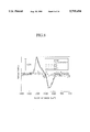
- FIG. 5 shows a graph showing the depth profile of the contaminant Al of the semiconductor substrates, prepared in the embodiment of the present invention, measured by XPS.
- FIG. 6A shows a graph showing the result of TRXF observation measured on the contaminated semiconductor substrates prepared in the embodiment of the present invention.
- FIG. 6B shows a graph explaining FIG. 6A.
- FIG. 7 shows a graph of relationships between contact angles with the semiconductor substrates cleaned by the semiconductor substrate cleaning method according to the embodiment of the present invention, and treatment temperatures.
- FIG. 8 shows FT-IR RAS spectra measured on the contaminated semiconductor substrate, cleaned by the semiconductor substrate cleaning method according to the embodiment of the present invention, before and after immersion in pure water having a lower dissolved oxygen concentration.
- FIG. 9 shows a graph of relationships between contact angles with the semiconductor substrates cleaned by the semiconductor substrate cleaning method according to the embodiment of the present invention, and treatment time.
- FIG. 10 shows FT-IR RAS spectra measured on the semiconductor substrate, cleaned by the semiconductor substrate cleaning method according to the embodiment of the present invention, before and after immersion in pure water having a lower dissolved oxygen concentration.
- FIG. 11 shows a graph of residual sulfuric acid ion amounts on semiconductor substrates cleaned by the semiconductor substrate cleaning method according to the embodiment of the present invention.
- FIG. 12 shows a schematic view of the semiconductor substrate cleaning equipment according to a first variation of the present invention.
- FIG. 13 shows a schematic view of the semiconductor substrate cleaning equipment according to a second variation of the present invention.
- FIG. 14 shows a schematic view of the semiconductor substrate cleaning equipment according to a third variation of the present invention.
- FIG. 1 is a diagrammatic view of the semiconductor substrate cleaning equipment used in the present embodiment.
- the cleaning equipment is enclosed by a box 10 so that the inside of the cleaning equipment is shielded from the outside air.
- a pure water bath 12 for cleaning semiconductor substrates, and a heater 14 which heats a cleaning liquid to be fed into the pure water bath 12.
- the pure water bath 12 has a pure water feed pipe 16 which supplies pure water into the pure water bath 12.
- the pure water feed pipe 16 is connected to a DO meter which detects dissolved oxygen concentrations in the pure water to be supplied into the pure water bath 12.
- a differential pressure gauge 28 which measures pressure differences between the outside of the box and the inside of the box 10, a nitrogen feed pipe 20 and an oxygen feed pipe 22, so that ambience in the inside of the box can be controlled.
- oxygen concentrations in the box 10 are monitored by an oxygen concentration meter 24 and are controlled to be below 25 ppm at 25° C.
- the inside of the cleaning equipment is thus shielded from the outside to control an ambience in the equipment because when pure water having a low dissolved oxygen content is left in normal atmospheric air, oxygen in the atmospheric air solves into the pure water, and the dissolved oxygen concentration cannot be kept low.
- the box 10 has a pass box 26 which prevents the outside air from coming into the box 10 when semiconductor substrates are loaded into the box 10.
- the semiconductor substrates are temporarily loaded in the pass box 26, and inside of the pass box 26 is replaced with an inert gas, e.g., nitrogen, and then the semiconductor substrates are loaded into the box 10.
- an inert gas e.g., nitrogen
- FIG. 2 shows the dependency of the amount of residual metallic contamination on the dissolved oxygen concentration in pure water.
- FIG. 3 shows the dependency of the amount of residual metallic contamination on the treatment temperature.
- FIG. 4 shows the dependency of the amount of residual metallic contamination on the treatment time.
- FIG. 2 shows dissolved oxygen concentration dependence with the cleaning effect measured in a case that semiconductor substrates were immersed in pure water for 30 minutes at a 100° C. pure water temperature.
- the intentionally contaminated semiconductor substrates were prepared by treating p-type and n-type (100)-oriented silicon substrates having a resistivity about 10 ⁇ -cm with hydrogen fluoride to remove oxide films on the surfaces of the semiconductor substrates, and then immersing the semiconductor substrates in an SC-1 solution added to an atomic absorption spectrometry standard solution containing Al, Cd, Co, Cr, Cu, Fe, Mg, Mn and Ni for chemical treatment.
- metallic contaminant amounts adsorbed on the surfaces of the semiconductor substrate was decreased by the cleaning of the semiconductor substrate with the pure water.
- the removing effect increased as the dissolved oxygen concentration in the pure water was decreased to 200 ppb and to 1 ppb. Especially when the dissolved oxygen concentration was decreased to 1 ppb, the effect was conspicuous, and the effect of removing the metallic contaminants except Cu could be drastically improved.
- FIG. 3 shows pure water temperature dependence with the cleaning effect when a dissolved oxygen concentration in the pure water was 1 ppb, and treatment time was 30 minutes.
- the metallic contaminant removing effect does not substantially depend on the treatment temperature.
- the adsorption amounts of metallic contaminants except Cu gradually decreased in 10 minutes of the treatment and decreased further with further increases of time of the immersion. But after 30 minutes of the treatment the adsorption amounts did not decrease, and thereafter no substantial changes took place in the adsorption amounts. Thus, the effect of removing metallic contaminants by the use of low dissolved-oxygen pure water is considered to reach an equilibrium.
- FIG. 5 shows the depth profile of the contaminant Al measured by XPS (X-ray photoelectron spectroscopy).
- FIG. 6A shows the result of TRXF (total reflection X-ray fluorescence analysis) observation on the contaminated semiconductor substrates.
- FIG. 6B shows a graph explaining FIG. 6A.
- FIG. 7 shows a graph of relationships between contact angles with the cleaned semiconductor substrates and treatment temperatures.
- FIG. 8 shows the change in the FT-IR RAS spectra after immersion in pure water having a lower dissolved oxygen concentration.
- FIG. 9 shows a graph of contact angles with the cleaned semiconductor substrates and treatment temperatures.
- FIG. 10 shows the change in the FT-IR RAS spectra after immersion in pure water having a lower dissolved oxygen concentration.
- FIG. 11 shows a graph of amounts of residual sulfuric acid ions on the cleaned semiconductor substrates.
- FIG. 5 shows the depth profile of the contaminant Al measured by XPS, of the surfaces of the semiconductor substrates immediately after contamination.
- the dotted line indicates interfaces between oxide films and the semiconductor substrates
- the one-dot chain line indicates the surfaces of the oxide films. As shown, it is found that Al of the metallic contaminants is present in the oxide films and near the surfaces.
- FIG. 6A shows the result of TRXF observation on the surfaces of the semiconductor substrate immediately after contamination.
- the metallic contamination has different peak positions depending on particle contamination or molecular surface contamination. All the metallic contaminants have increasing intensities with increases of incident angles of X-rays, in which the metallic contaminants are present in molecular states.
- FIG. 7 shows the dependence of treatment temperature and contact angle with the wafer surfaces with a dissolved oxygen concentration in the pure water set at 1 ppb and with treatment time set at 30 minutes.
- the surfaces of the semiconductor substrates are hydrophilic because of grown oxide films, i.e., they have small contact angles (indicated by ⁇ in FIG. 7).
- contact angles gradually increased. The changes were small at temperatures below 90° C., and the semiconductor substrate surfaces remained hydrophilic. But when the treatment temperature was above 100° C., contact angles greatly increased, and the semiconductor substrate surfaces changed to be hydrophobic.
- the surface conditions of the semiconductor substrates at this time were estimated by FT-IR. As shown in FIG. 8, it was found that a peak of Si--O bonds observed at treatment temperatures below 70° C. disappeared at a 100° C. treatment temperature, and oxide films were removed.
- FIG. 11 shows the amounts of residual sulfuric acid ion after the semiconductor substrates were immersed in a mixed liquid of hydrogen peroxide and sulfuric acid and then cleaned with various kinds of pure water.
- Treatment A is a treatment with 8 ppb dissolved-oxygen concentration in pure water of 25° C. after a chemical treatment.
- Treatment B is a treatment with 1 ppb dissolved-oxygen concentration in pure water of 25° C.
- Treatment C is a treatment with 1 ppb dissolved-oxygen concentration in pure water at 100° C. after a chemical treatment.
- a reference wafer was treated with a mixed liquid of ammonium and hydrogen peroxide, and next treated with nitric acid.
- Treatment C could reduce a residual sulfuric acid ion density down to about 1/10 that of treatments A and B, which was substantially the same as a residual sulfuric acid ion density of Reference wafer.
- the semiconductor substrates are immersed in the pure water heated to a temperature above 60° C. in an atmosphere which allows the dissolved-oxygen concentration in the pure water to be kept for etching of oxide films formed on the surfaces of the semiconductor, whereby the surfaces of the semiconductor substrates were cleaned. Accordingly, contaminants and residual chemicals can be effectively removed without adding chemical treatment steps.
- the cleaning of semiconductor substrates by the use of low dissolved-oxygen concentration in pure water does not use chemicals of high viscosities.
- the surfaces of semiconductor substrates can be cleaned without residual chemicals.
- Water cleaning with the above-described low dissolved-oxygen concentration in pure water following a chemical treatment can effectively reduce residual chemicals in comparison with water cleaning with pure water having a dissolved oxygen concentration not controlled or dissolved oxygen pure water at below 60° C.
- the cleaning method can remove contaminants without residual chemicals, whereby semiconductor devices of high quality can be provided without lowering product yields.
- cleaning of semiconductor substrates with the so-called chemical oxide films formed by SC-1 treatment was explained.
- cleaning with low dissolved-oxygen pure water which is effected by etching oxide films on the surfaces of semiconductor substrates, may be used in removing native oxide films formed by leaving semiconductor substrates in an atmosphere containing oxygen or immersing the semiconductor substrates in pure water with a higher dissolved-oxygen amount.
- cleaning is conducted with low dissolved-oxygen pure water for cleaning of the surfaces of semiconductor substrates concurrent with removal of native oxide films.
- contaminants adhered to the surfaces of semiconductor substrates can be removed by immersing for more than 10 minutes in pure water of a below 200 ppb dissolved oxygen concentration which has been heated to above 60° C., and it is preferred that parameters to this end are optimized based on device structures.
- a temperature of the pure water and a period of time during which semiconductor substrates are immersed are set so that a contact angle formed between the pure water and the semiconductor substrates after cleaning of the semiconductor substrates is above 70° which is formed between pure water and a silicon substrate, with no oxide film formed thereon, whereby all oxide films can be removed. Contaminants on the surfaces of semiconductor substrates can be effectively removed.
- semiconductor substrate cleaning equipment is constituted with a chemical bath 30, and a pure water bath 12 provided in the closed unit of a box 10 or the like disposed in a usual draft chamber, so that semiconductor substrates 32 are subjected to a chemical treatment in the chemical bath 30, then loaded into the closed unit in which an atmosphere of an adjusted oxygen concentration is established, and are subjected to water cleaning by low dissolved-oxygen pure water in the pure water bath 12.
- a pass box 26 is provided between the closed unit and the outside air as shown in FIG. 1, whereby the cleaning can be conducted without disturbing the gas atmosphere in the closed unit.
- the chemical bath 30 and the pure water bath 12 are disposed in the same closed unit with an atmosphere having an adjusted oxygen concentration.
- an atmosphere in the box 10 was controlled so that an oxygen concentration was below 25 ppm in 25° C. atmospheric pressure. But it is preferred to control the oxygen concentration in an atmosphere so that the oxygen concentration in the closed unit can keep a dissolved oxygen concentration in the pure water. That is, the oxygen concentration in an atmosphere is controlled so as to satisfy Henry's law.
- the pure water bath is provided in the closed unit to prevent outside oxygen from solving in the low dissolved-oxygen pure water for obtaining a high cleaning effect. It is not essential to close in the pure water bath with the closed unit as long as the cleaning equipment is so constituted that the low dissolved-oxygen pure water is kept out of contact with outside oxygen.
- one or a plurality of inert gas injection ports 34 are provided above the pure water bath 12, so that inert gas streams 36 which cover the surface of the pure water bath 12 with the inert gas are generated. Outside air does not solve into the low dissolved-oxygen pure water, and semiconductor substrates can be cleaned with a dissolved oxygen concentration kept low.
- inert gas injection ports are provided in the walls of the pure water bath, or near the pure water bath and above the surface of the pure water, and inert gas exhaust ports are provided opposed to the injection ports across the pure water bath, so that the inert gas is caused to flow horizontally.
- the low dissolved-oxygen pure water is heated by the heater 14 provided in the pure water bath 12. But as shown in FIGS. 12 and 13, pure water may be heated through heating means 38 before being fed into the cleaning equipment. In this case, overflow rinse, etc. are possible with the low dissolved oxygen pure water, whereby removed contaminants do not remain in the pure water bath 12, which may enhances the contaminant removing effect.
Applications Claiming Priority (2)
| Application Number | Priority Date | Filing Date | Title |
|---|---|---|---|
| JP6-314392 | 1994-12-19 | ||
| JP6314392A JPH08172068A (ja) | 1994-12-19 | 1994-12-19 | 半導体基板の洗浄方法及び半導体装置の製造方法 |
Publications (1)
| Publication Number | Publication Date |
|---|---|
| US5795494A true US5795494A (en) | 1998-08-18 |
Family
ID=18052798
Family Applications (1)
| Application Number | Title | Priority Date | Filing Date |
|---|---|---|---|
| US08/513,748 Expired - Fee Related US5795494A (en) | 1994-12-19 | 1995-08-10 | Semiconductor substrate cleaning method and semiconductor device fabrication method |
Country Status (6)
| Country | Link |
|---|---|
| US (1) | US5795494A (ja) |
| EP (1) | EP0718872B1 (ja) |
| JP (1) | JPH08172068A (ja) |
| KR (1) | KR0185463B1 (ja) |
| CN (1) | CN1079579C (ja) |
| DE (1) | DE69507445T2 (ja) |
Cited By (8)
| Publication number | Priority date | Publication date | Assignee | Title |
|---|---|---|---|---|
| US6200196B1 (en) | 1997-12-04 | 2001-03-13 | Micron Technology, Inc. | Polishing systems, methods of polishing substrates, and methods of preparing liquids for semiconductor fabrication processes |
| US6509305B1 (en) * | 1997-06-24 | 2003-01-21 | Tadahiro Ohmi | Method for preparing cleaning solution |
| US20030137052A1 (en) * | 2000-06-23 | 2003-07-24 | Fujitsu Limited | Semiconductor device and method of manufacture thereof |
| US6637445B2 (en) * | 2000-12-12 | 2003-10-28 | S.E.S. Company Limited | Substrate processing unit |
| US20100083985A1 (en) * | 2008-10-08 | 2010-04-08 | Shin-Etsu Chemical Co., Ltd. | Method for cleaning photomask-related substrate, cleaning method, and cleaning fluid supplying apparatus |
| US20180039170A1 (en) * | 2015-02-27 | 2018-02-08 | Canon Kabushiki Kaisha | Nanonimprint liquid material, method for manufacturing nanoimprint liquid material, method for manufacturing cured product pattern, method for manufacturing optical component, and method for manufacturing circuit board |
| US20190186033A1 (en) * | 2013-03-14 | 2019-06-20 | Xtalic Corporation | Electrodeposition in ionic liquid electrolytes |
| US10861718B2 (en) | 2018-01-15 | 2020-12-08 | SCREEN Holdings Co., Ltd. | Substrate processing method and substrate processing apparatus |
Families Citing this family (8)
| Publication number | Priority date | Publication date | Assignee | Title |
|---|---|---|---|---|
| US8226775B2 (en) * | 2007-12-14 | 2012-07-24 | Lam Research Corporation | Methods for particle removal by single-phase and two-phase media |
| JP2010117412A (ja) * | 2008-11-11 | 2010-05-27 | Shin-Etsu Chemical Co Ltd | フォトマスク関連基板の洗浄方法 |
| JP2010117403A (ja) * | 2008-11-11 | 2010-05-27 | Shin-Etsu Chemical Co Ltd | フォトマスク関連基板の洗浄方法 |
| JP5871652B2 (ja) * | 2012-02-23 | 2016-03-01 | オルガノ株式会社 | アルコール中の溶存酸素除去方法、アルコール供給装置並びに洗浄液供給装置 |
| CN102728577B (zh) * | 2012-06-21 | 2014-11-19 | 信义汽车部件(芜湖)有限公司 | 一种提高玻璃塑料附件表面张力的工艺方法 |
| US9339853B2 (en) | 2012-12-04 | 2016-05-17 | The Boeing Company | Surface materials for decontamination with decontaminants |
| CN111599730A (zh) * | 2020-06-22 | 2020-08-28 | 上海华力微电子有限公司 | 刻蚀液供给装置及方法 |
| CN116435418B (zh) * | 2023-06-13 | 2023-08-25 | 南昌凯捷半导体科技有限公司 | 一种590nm反极性LED外延片及其制备方法 |
Citations (13)
| Publication number | Priority date | Publication date | Assignee | Title |
|---|---|---|---|---|
| SU843029A1 (ru) * | 1979-04-16 | 1981-06-30 | Предприятие П/Я А-3560 | Устройство дл очистки поверхностипОлупРОВОдНиКОВыХ плАСТиН |
| US4722752A (en) * | 1986-06-16 | 1988-02-02 | Robert F. Orr | Apparatus and method for rinsing and drying silicon wafers |
| JPH01150328A (ja) * | 1987-12-07 | 1989-06-13 | Matsushita Electric Ind Co Ltd | 半導体基板の処理方法 |
| JPH02164035A (ja) * | 1988-12-19 | 1990-06-25 | Nec Corp | 半導体基板の洗浄方法 |
| JPH03157927A (ja) * | 1989-11-15 | 1991-07-05 | Mitsubishi Electric Corp | 半導体ウエハ乾燥方法 |
| JPH0440270A (ja) * | 1990-06-01 | 1992-02-10 | Miura Co Ltd | 電子部品の洗浄方法 |
| JPH04124825A (ja) * | 1990-09-14 | 1992-04-24 | Sharp Corp | 半導体ウエハの洗浄方法 |
| JPH04151835A (ja) * | 1990-05-25 | 1992-05-25 | Shimada Phys & Chem Ind Co Ltd | 洗浄乾燥方法 |
| US5176756A (en) * | 1990-08-29 | 1993-01-05 | Fujitsu Limited | Method for fabricating a semiconductor device including a step for cleaning a semiconductor substrate |
| JPH0653201A (ja) * | 1992-07-27 | 1994-02-25 | Nippon Telegr & Teleph Corp <Ntt> | 化合物半導体基板の表面形成法 |
| DE4340589A1 (de) * | 1992-12-24 | 1994-06-30 | Gold Star Electronics | Verfahren zur Reinigung von Halbleiterbauelementen |
| US5451267A (en) * | 1993-05-13 | 1995-09-19 | Wacker Chemitronic Gesellschaft Fur Elektronik-Grundstoffe Mbh | Process for the wet-chemical treatment of disk-shaped workpieces |
| US5464480A (en) * | 1993-07-16 | 1995-11-07 | Legacy Systems, Inc. | Process and apparatus for the treatment of semiconductor wafers in a fluid |
-
1994
- 1994-12-19 JP JP6314392A patent/JPH08172068A/ja active Pending
-
1995
- 1995-07-15 KR KR1019950020893A patent/KR0185463B1/ko not_active IP Right Cessation
- 1995-08-10 US US08/513,748 patent/US5795494A/en not_active Expired - Fee Related
- 1995-08-14 EP EP95305651A patent/EP0718872B1/en not_active Expired - Lifetime
- 1995-08-14 DE DE69507445T patent/DE69507445T2/de not_active Expired - Fee Related
- 1995-08-18 CN CN95115566A patent/CN1079579C/zh not_active Expired - Fee Related
Patent Citations (14)
| Publication number | Priority date | Publication date | Assignee | Title |
|---|---|---|---|---|
| SU843029A1 (ru) * | 1979-04-16 | 1981-06-30 | Предприятие П/Я А-3560 | Устройство дл очистки поверхностипОлупРОВОдНиКОВыХ плАСТиН |
| US4722752A (en) * | 1986-06-16 | 1988-02-02 | Robert F. Orr | Apparatus and method for rinsing and drying silicon wafers |
| JPH01150328A (ja) * | 1987-12-07 | 1989-06-13 | Matsushita Electric Ind Co Ltd | 半導体基板の処理方法 |
| JPH02164035A (ja) * | 1988-12-19 | 1990-06-25 | Nec Corp | 半導体基板の洗浄方法 |
| JPH03157927A (ja) * | 1989-11-15 | 1991-07-05 | Mitsubishi Electric Corp | 半導体ウエハ乾燥方法 |
| JPH04151835A (ja) * | 1990-05-25 | 1992-05-25 | Shimada Phys & Chem Ind Co Ltd | 洗浄乾燥方法 |
| JPH0440270A (ja) * | 1990-06-01 | 1992-02-10 | Miura Co Ltd | 電子部品の洗浄方法 |
| US5176756A (en) * | 1990-08-29 | 1993-01-05 | Fujitsu Limited | Method for fabricating a semiconductor device including a step for cleaning a semiconductor substrate |
| JPH04124825A (ja) * | 1990-09-14 | 1992-04-24 | Sharp Corp | 半導体ウエハの洗浄方法 |
| JPH0653201A (ja) * | 1992-07-27 | 1994-02-25 | Nippon Telegr & Teleph Corp <Ntt> | 化合物半導体基板の表面形成法 |
| DE4340589A1 (de) * | 1992-12-24 | 1994-06-30 | Gold Star Electronics | Verfahren zur Reinigung von Halbleiterbauelementen |
| US5567244A (en) * | 1992-12-24 | 1996-10-22 | Goldstar Electron Co., Ltd. | Process for cleaning semiconductor devices |
| US5451267A (en) * | 1993-05-13 | 1995-09-19 | Wacker Chemitronic Gesellschaft Fur Elektronik-Grundstoffe Mbh | Process for the wet-chemical treatment of disk-shaped workpieces |
| US5464480A (en) * | 1993-07-16 | 1995-11-07 | Legacy Systems, Inc. | Process and apparatus for the treatment of semiconductor wafers in a fluid |
Non-Patent Citations (2)
| Title |
|---|
| Journal of the Electrochemical Society, vol. 140, No. 3, Mar. 1993, T. Ohmi et al., "Native Oxide Growth and Organic Impurity Removal on Si Surface with Ozone-Injected Ultrapure Water"--pp. 804-810. |
| Journal of the Electrochemical Society, vol. 140, No. 3, Mar. 1993, T. Ohmi et al., Native Oxide Growth and Organic Impurity Removal on Si Surface with Ozone Injected Ultrapure Water pp. 804 810. * |
Cited By (14)
| Publication number | Priority date | Publication date | Assignee | Title |
|---|---|---|---|---|
| US6509305B1 (en) * | 1997-06-24 | 2003-01-21 | Tadahiro Ohmi | Method for preparing cleaning solution |
| US6716802B1 (en) | 1997-12-04 | 2004-04-06 | Micron Technology, Inc. | Polishing systems, methods of polishing substrates, and methods of preparing liquids for semiconductor fabrication processes |
| US6206757B1 (en) * | 1997-12-04 | 2001-03-27 | Micron Technology, Inc. | Polishing systems, methods of polishing substrates, and methods of preparing liquids for semiconductor fabrication processes |
| US6200196B1 (en) | 1997-12-04 | 2001-03-13 | Micron Technology, Inc. | Polishing systems, methods of polishing substrates, and methods of preparing liquids for semiconductor fabrication processes |
| US6719823B2 (en) | 1997-12-04 | 2004-04-13 | Micron Technology, Inc. | Polishing systems, methods of polishing substrates, and methods of cleaning polishing slurry from substrate surfaces |
| US20030137052A1 (en) * | 2000-06-23 | 2003-07-24 | Fujitsu Limited | Semiconductor device and method of manufacture thereof |
| US6943115B2 (en) * | 2000-06-23 | 2005-09-13 | Fujitsu Limited | Semiconductor device and method of manufacture thereof |
| US6637445B2 (en) * | 2000-12-12 | 2003-10-28 | S.E.S. Company Limited | Substrate processing unit |
| US20100083985A1 (en) * | 2008-10-08 | 2010-04-08 | Shin-Etsu Chemical Co., Ltd. | Method for cleaning photomask-related substrate, cleaning method, and cleaning fluid supplying apparatus |
| US8956463B2 (en) | 2008-10-08 | 2015-02-17 | Shin-Etsu Chemical Co., Ltd. | Method for cleaning photomask-related substrate, cleaning method, and cleaning fluid supplying apparatus |
| US20190186033A1 (en) * | 2013-03-14 | 2019-06-20 | Xtalic Corporation | Electrodeposition in ionic liquid electrolytes |
| US20180039170A1 (en) * | 2015-02-27 | 2018-02-08 | Canon Kabushiki Kaisha | Nanonimprint liquid material, method for manufacturing nanoimprint liquid material, method for manufacturing cured product pattern, method for manufacturing optical component, and method for manufacturing circuit board |
| US10861718B2 (en) | 2018-01-15 | 2020-12-08 | SCREEN Holdings Co., Ltd. | Substrate processing method and substrate processing apparatus |
| US11222795B2 (en) | 2018-01-15 | 2022-01-11 | SCREEN Holdings Co., Ltd. | Substrate processing method and substrate processing apparatus |
Also Published As
| Publication number | Publication date |
|---|---|
| DE69507445T2 (de) | 1999-06-02 |
| CN1079579C (zh) | 2002-02-20 |
| JPH08172068A (ja) | 1996-07-02 |
| EP0718872B1 (en) | 1999-01-20 |
| EP0718872A1 (en) | 1996-06-26 |
| DE69507445D1 (de) | 1999-03-04 |
| CN1127424A (zh) | 1996-07-24 |
| KR960026331A (ko) | 1996-07-22 |
| KR0185463B1 (ko) | 1999-04-15 |
Similar Documents
| Publication | Publication Date | Title |
|---|---|---|
| US5795494A (en) | Semiconductor substrate cleaning method and semiconductor device fabrication method | |
| JP3154814B2 (ja) | 半導体ウエハの洗浄方法および洗浄装置 | |
| US6132522A (en) | Wet processing methods for the manufacture of electronic components using sequential chemical processing | |
| US6983756B2 (en) | Substrate treatment process and apparatus | |
| EP0731498B1 (en) | Surface processing method for silicon substrates | |
| US6491763B2 (en) | Processes for treating electronic components | |
| WO2002099394A1 (en) | Methods and systems for monitoring process fluids | |
| US5332444A (en) | Gas phase cleaning agents for removing metal containing contaminants from integrated circuit assemblies and a process for using the same | |
| US5092937A (en) | Process for treating semiconductors | |
| WO2001040124A1 (en) | Apparatus for providing ozonated process fluid and methods for using same | |
| EP0690484B1 (en) | Method of manufacturing semiconductor device and methods of processing, analyzing and manufacturing its substrate | |
| JPH0878372A (ja) | 有機物除去方法及びその装置 | |
| EP0618612A2 (en) | Method of cleaning semiconductor device and equipment for cleaning semiconductor device | |
| JP2002100634A (ja) | アニールウェーハの製造方法およびアニールウェーハ | |
| KR19980047233A (ko) | 극히 깨끗한 물로 린스하지 않고 직접 화학 용기에서 웨이퍼를 건조시키는 방법 | |
| US20030011774A1 (en) | Methods and systems for monitoring process fluids | |
| EP2284873B1 (en) | Method for manufacturing semiconductor device and method for cleaning semiconductor substrate | |
| JP2003218085A (ja) | 半導体基板の洗浄方法 | |
| JP2713787B2 (ja) | 半導体の湿式洗浄方法 | |
| US6495099B1 (en) | Wet processing methods for the manufacture of electronic components | |
| EP1508385B1 (en) | System for ultraviolet cleaning | |
| Murarka et al. | Contamination of silicon and oxidized silicon wafers during plasma etching | |
| JPH06177102A (ja) | 化合物半導体表面の清浄化方法および装置 | |
| JP3329902B2 (ja) | 表面処理方法及び表面処理装置 | |
| KR0172717B1 (ko) | 반도체 기판의 세정방법 |
Legal Events
| Date | Code | Title | Description |
|---|---|---|---|
| FEPP | Fee payment procedure |
Free format text: PAYOR NUMBER ASSIGNED (ORIGINAL EVENT CODE: ASPN); ENTITY STATUS OF PATENT OWNER: LARGE ENTITY |
|
| FPAY | Fee payment |
Year of fee payment: 4 |
|
| REMI | Maintenance fee reminder mailed | ||
| LAPS | Lapse for failure to pay maintenance fees | ||
| STCH | Information on status: patent discontinuation |
Free format text: PATENT EXPIRED DUE TO NONPAYMENT OF MAINTENANCE FEES UNDER 37 CFR 1.362 |
|
| FP | Lapsed due to failure to pay maintenance fee |
Effective date: 20060818 |