US5561074A - Method for fabricating reverse-staggered thin-film transistor - Google Patents
Method for fabricating reverse-staggered thin-film transistor Download PDFInfo
- Publication number
- US5561074A US5561074A US08/425,806 US42580695A US5561074A US 5561074 A US5561074 A US 5561074A US 42580695 A US42580695 A US 42580695A US 5561074 A US5561074 A US 5561074A
- Authority
- US
- United States
- Prior art keywords
- forming
- layer
- semiconductor
- channel layer
- film transistor
- Prior art date
- Legal status (The legal status is an assumption and is not a legal conclusion. Google has not performed a legal analysis and makes no representation as to the accuracy of the status listed.)
- Expired - Lifetime
Links
Images


Classifications
-
- H—ELECTRICITY
- H10—SEMICONDUCTOR DEVICES; ELECTRIC SOLID-STATE DEVICES NOT OTHERWISE PROVIDED FOR
- H10D—INORGANIC ELECTRIC SEMICONDUCTOR DEVICES
- H10D30/00—Field-effect transistors [FET]
- H10D30/01—Manufacture or treatment
- H10D30/021—Manufacture or treatment of FETs having insulated gates [IGFET]
- H10D30/031—Manufacture or treatment of FETs having insulated gates [IGFET] of thin-film transistors [TFT]
- H10D30/0312—Manufacture or treatment of FETs having insulated gates [IGFET] of thin-film transistors [TFT] characterised by the gate electrodes
- H10D30/0316—Manufacture or treatment of FETs having insulated gates [IGFET] of thin-film transistors [TFT] characterised by the gate electrodes of lateral bottom-gate TFTs comprising only a single gate
-
- H—ELECTRICITY
- H10—SEMICONDUCTOR DEVICES; ELECTRIC SOLID-STATE DEVICES NOT OTHERWISE PROVIDED FOR
- H10P—GENERIC PROCESSES OR APPARATUS FOR THE MANUFACTURE OR TREATMENT OF DEVICES COVERED BY CLASS H10
- H10P10/00—Bonding of wafers, substrates or parts of devices
-
- H—ELECTRICITY
- H10—SEMICONDUCTOR DEVICES; ELECTRIC SOLID-STATE DEVICES NOT OTHERWISE PROVIDED FOR
- H10D—INORGANIC ELECTRIC SEMICONDUCTOR DEVICES
- H10D30/00—Field-effect transistors [FET]
- H10D30/01—Manufacture or treatment
- H10D30/021—Manufacture or treatment of FETs having insulated gates [IGFET]
- H10D30/031—Manufacture or treatment of FETs having insulated gates [IGFET] of thin-film transistors [TFT]
- H10D30/0321—Manufacture or treatment of FETs having insulated gates [IGFET] of thin-film transistors [TFT] comprising silicon, e.g. amorphous silicon or polysilicon
-
- H—ELECTRICITY
- H10—SEMICONDUCTOR DEVICES; ELECTRIC SOLID-STATE DEVICES NOT OTHERWISE PROVIDED FOR
- H10D—INORGANIC ELECTRIC SEMICONDUCTOR DEVICES
- H10D30/00—Field-effect transistors [FET]
- H10D30/60—Insulated-gate field-effect transistors [IGFET]
- H10D30/67—Thin-film transistors [TFT]
Definitions
- the present invention relates to a method for fabricating a thin-film transistor and, more particularly, to a method for fabricating a reverse-staggered thin-film transistor employed in a liquid crystal display device.
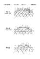
- FIG. 1 shows a conventional thin-film transistor of an amorphous silicon.
- This thin-film transistor is constituted by a gate electrode 2, a gate insulating film 3 made of a silicon nitride film, an intrinsic amorphous silicon layer 4 and an n-type amorphous silicon contact layer 5, a drain electrode 6, a source electrode 7.
- a protective layer 9 made of silicon nitride is further formed to cover the transistor.
- the surface portion 10 of the amorphous silicon layer 4 between the drain electrode 6 and the source electrode 7 is sometimes called a "back channel" and has one of key factors determining the characteristics of the transistor.
- a leak current is caused to increase and flows between the source and drain. Even if the back channel 10 is not contaminated, the positive electric charges due to the contamination on the protective film 9 increase an electric field applied the back channel 10 up to or more than the threshold of the back channel. A leakage current thereby flows.
- the protective film 9 itself may be positively charged, so that the leak current also flows.
- a thin-film transistor is disclosed in Japanese Patent Laid-Open No. Hei 2-163972 that has a back channel covered with an oxide film obtained from hydrogen peroxide or with an alumina film formed by the CVD process. Such a film can convert the back channel into a p-type one. The leakage current is thereby decreased.
- the p-type back channel thus converted depends on the quality of the oxide or the alumina film and is thus inferior in controllability.
- the drain and source electrodes are damaged by the hydrogen peroxide.
- alumina in the alumina film may be diffused into the amorphous silicon layer to change the property of a thin-film transistor.
- FIG. 2 there is shown another thin-film transistor which is disclosed in Japanese Patent Publication No. Hei 5-0083197, in which the same constituents as those shown in FIG. 4 are denoted by the same reference numerals.
- a portion of the n-type contact layer 5 which is not covered with the drain and source electrodes 6 and 7 is converted into a p-type region 11 by adding p-type impurities therein.
- the back channel is thereby covered with the p-type region 11.
- the contact layer 5 has a considerably high impurity concentration of 10 20 atoms/cm 3 or more. For this reason, it is necessary to dope the p-type impurities at a very high concentration. Such very high doping lacks in controllability, however. Moreover, the very highly doped region 11 results in increase of the leakage current.
- the thin-film transistor fabrication method of the present invention it is possible to provide a structure in which a p-type amorphous silicon layer or a p-type polysilicon layer is formed uniformly on an intrinsic amorphous silicon layer directly.
- the method has an advantage of preventing the leak current of a transistor which is increased due to contamination by cations coming from the outside and electron generation in a back channel by electrification of the protective film. Moreover, because p-type amorphous silicon or p-type polysilicon can selectively be deposited on amorphous or polysilicon by exposing it to the gaseous phase of disilane containing diborane or silane, and there is no such side reaction as effected wiring, aluminum diffusion in an amorphous or polysilicon layer, or difficult process control, and a large advantage can be obtained. When using the plasma CVD process, there is an advantage that the film forming rate is high though the selectivity is low.
- the method of the present invention for fabricating a thin-film transistor is characterized in that a p-type amorphous silicon layer with a thickness of 100 ⁇ or less containing no n-type doped impurities is formed on a back channel of the intrinsic amorphous silicon directly. Because of the absence n-type doped impurities, impurity density of the p-type amorphous silicon layer is not so high that prevents current leakage according to non-uniform ion distribution of the layer. Furthermore, it gets more uniformal ion distribution according to obtaining by gaseous phase of disilane or silane gas containing diborane.
- the method of the present invention is characterized in that the p-type amorphous silicon layer can be obtained by exposing the intrinsic amorphous silicon layer to the gaseous phase of disilane or silane gas containing diborane. Furthermore, it is possible to use polysilicon instead of amorphous silicon.
- FIG. 1 is a sectional view of a thin-film transistor according to a prior art
- FIG. 2 is a sectional view of a thin-film transistor according to another prior art
- FIG. 3 is a sectional view illustrative of a thin-film transistor fabricated by a method according to an embodiment of the present invention
- FIGS. 4(a) to 4(d) are sectional views illustrative of respective steps of a method according to the embodiment of the present invention.
- FIG. 5 is a graph indicative of comparison in a source-drain current between the thin-film transistor shown in FIG. 1 and that shown in FIG. 1 or FIG. 2;
- FIG. 6 is a sectional view illustrative of a thin-film transistor fabricated by a method according to another embodiment of the present invention.
- a thin-film transistor fabricated by a method according an embodiment of the present invention has a gate electrode 2 selectively formed on an insulating substrate 1.
- the transistor further comprises a gate insulating film 3, an intrinsic or non-doped amorphous silicon layer 4, an n-type amorphous silicon contact layer 5, a drain electrode 6, and a source electrode 7.
- This transistor further has a p-type amorphous silicon layer 8 on the back channel portion of the amorphous silicon layer 4 between the drain electrode 6 and the source electrode 7 in accordance with the present invention.
- the thickness of p-type amorphous silicon layer 8 is 100 ⁇ or less.
- a protective material such as silicon-nitride covers the p-type amorphous silicon layer 4 and a the source and drain electrodes 6 and 7 in contact therewith.
- the above thin-film transistor is fabricated as follows:
- the gate electrode 2 made of a metal such as chromium is selectively formed on the insulating substrate 1 made of a glass or the like, followed by forming the gate insulating film 3 made of silicon nitride over the entire surface.
- the intrinsic or non-doped amorphous silicon layer 4 and the n-type amorphous silicon contact layer 5 are thereafter deposited in that order by the plasma CVD method.
- the amorphous silicon layer 4 and the n-type amorphous silicon contact layer 5 are selectively etched to form an island by the lithography art, as shown in FIG. 4 (b) .
- a metal film made of chromium or the like is deposited over the entire surface by the sputtering method and then patterned to form the drain electrode 6 and the source electrode 7 as shown in FIG. 4 (c).
- the portion of the n-type amorphous silicon contact layer 5 between the drain electrode 6 and the source electrode 7 is removed by using the electrodes as a mask by the wet etching method or the dry etching method in accordance with the present invention. This etching process is carried out until the surface portion of the amorphous silicon layer 4 is exposed. That portion of the contact layer 5 is thus completely removed, the surface of the amorphous silicon layer 4 thus exposed serves as a back channel 10, as shown in FIG. 4(d).
- the p-type amorphous silicon layer 8 is then selectively deposited between the drain electrode 6 and the source electrode 7 in accordance with the present invention. Finally the silicon-nitride protective film 9 is formed.
- the selective deposition of the p-type amorphous silicon layer 8 only on the exposed amorphous silicon layer is performed by mixing disilane Si 2 H 6 , hydrogen H 2 and diborane B 2 H 6 at the ratio of 3:2:6, setting the pressure of the mixed gas to 200 Pa and the substrate temperature to 350° C., and exposing the thin-film transistor shown in FIG. 4(d) to the mixed-gas atmosphere.
- the thickness of the layer 8 is several tens of angstroms though it cannot accurately be measured because the deposition rate is very low. Under the above conditions, the depositing time for the layer 8 can be approx. 15 min. Thereafter, the layer 8 is annealed in the nitrogen atmosphere at 250° C. for 30 min.
- silane instead of disilane in the mixed gas.
- silane is not easily decomposed only by raising the temperature. Therefore, it is better to use disilane.
- the ratio of disilane Si 2 H 6 to diborane B 2 H 6 of the mixed gas is set to 1:2.
- the ratio of hydrogen gas can be changed within the range of 0 to 10 when the ratio of disilane as 1.
- an inert gas such as argon
- the temperature of the substrate in the range of 300° to 400° C.
- the annealing time is approximately 30 min to 2 hr.
- the p-type amorphous silicon layer 8 is obtained at a very low deposition rate, it is easily influenced by a substrate due to the same effect as the epitaxial art for single-crystal silicon and thus it is selectively deposited only on the intrinsic amorphous silicon layer 4. Therefore, the layer 8 is preferable because it is hardly deposited on areas of the substrate other than the intrinsic amorphous silicon layer 4. Presence of the p-type amorphous silicon layer 8 can be confirmed by measuring the depth profile through the SIMS element analysis and it is found that boron is present in layers with a thickness of 50 ⁇ or less at a concentration of 10 18 to 10 19 atoms/cm 3 .
- FIG. 5 shows the property of the thin-film transistor of this embodiment.
- the current between drain and source to the gate voltage when applying the voltage of 10 V between the drain and source. From FIG. 5, it is understood that the current between the drain and the source is decreased for the gate voltage of -10 v to 0 V compared to the case of the prior art. That is, the leak current is decreased when the thin-film transistor is off.
- increase of the off current is not recognized even by applying +30 V to the gate electrode and 0 V to the source electrode for 90 min in an air temperature of 80° C. This is because the p-type silicon layer directly contacts the silicon-nitride protective film 9 and a stable interface is formed.
- the p-type amorphous silicon layer 8 with a thickness of several tens of angstroms is formed by mixing silane SiH 4 , hydrogen H 2 , and diborane B 2 H 6 at a mixing ratio of 1:1:2, setting the pressure of the mixed gas to 0.75 Torr, the substrate temperature to 300° C., and the electric power to 25 mW/cm 2 , and discharging electricity for 10 sec.
- the plasma CVD process an advantage is obtained that a p-type amorphous silicon layer can be formed for several tens of seconds though the selectivity is low.
- disilane and diborane for the vapor-phase epitaxy process.
- plasma CVD it is better to use silane and diborane.
- disilane for the plasma CVD.
- disilane is more easily decomposed than silane and therefore it is extremely decomposed due to plasma, disilane is less suitable for the plasma CVD.
- plasma CVD plasma serves as an assistant to decompose silane. Therefore, the combination of disilane and diborane in the vapor-phase epitaxy process corresponds to the combination of silane and diborane in the plasma CVD process.
- the mixing ratio of silane SiH 4 to diborane B 2 H 6 is set to 1:2 and hydrogen H 2 is mixed with the mixture of them in the range of 0 to 5.
- the pressure, substrate temperature, and electric power can be changed in the ranges of 80 to 120 Pa, 250° to 320° C., and 10 to 30 mW/cm 2 respectively. It is necessary to set the discharge time to several seconds to 1 min.
- FIG. 6 there is shown a thin-film transistor fabricated by a method according to another embodiment of the present invention, in which the same constituents as those shown in FIGS. 3 and 4 are denoted by the same reference numerals to omit the further description thereof.
- a p-type layer is denoted by the reference numeral 18 and thus formed by implanting or diffusing p-type impurities into the back channel portion of the layer 4. That is, after the step as shown in FIG. 4(d), boron ions are implanted by using the drain and source electrodes 6 and 7 as a mask. The annealing is then carried out to thereby form the p-type layer 18.
- the above embodiment shows a case of using amorphous silicon.
- a thin-film transistor made of polysilicon instead of amorphous silicon.
- the p-type polysilicon fabrication method is completely the same as the case of amorphous silicon described above.
Landscapes
- Thin Film Transistor (AREA)
Applications Claiming Priority (2)
| Application Number | Priority Date | Filing Date | Title |
|---|---|---|---|
| JP6-084229 | 1994-04-22 | ||
| JP8422994 | 1994-04-22 |
Publications (1)
| Publication Number | Publication Date |
|---|---|
| US5561074A true US5561074A (en) | 1996-10-01 |
Family
ID=13824652
Family Applications (1)
| Application Number | Title | Priority Date | Filing Date |
|---|---|---|---|
| US08/425,806 Expired - Lifetime US5561074A (en) | 1994-04-22 | 1995-04-20 | Method for fabricating reverse-staggered thin-film transistor |
Country Status (5)
| Country | Link |
|---|---|
| US (1) | US5561074A (enExample) |
| EP (1) | EP0678907B1 (enExample) |
| KR (1) | KR0180323B1 (enExample) |
| DE (1) | DE69525558T2 (enExample) |
| TW (1) | TW291597B (enExample) |
Cited By (15)
| Publication number | Priority date | Publication date | Assignee | Title |
|---|---|---|---|---|
| WO1998057506A1 (en) * | 1997-06-12 | 1998-12-17 | Northern Telecom Limited | Directory service based on geographic location of a mobile telecommunications unit |
| US5910019A (en) * | 1995-03-06 | 1999-06-08 | Nec Corporation | Method of producing silicon layer having surface controlled to be uneven or even |
| US6437368B2 (en) | 2000-02-18 | 2002-08-20 | Sharp Kabushiki Kaisha | Thin film transistor |
| US6461901B1 (en) * | 1996-08-29 | 2002-10-08 | Nec Corporation | Method of forming a thin-film transistor having a high resistance back channel region |
| CN100477129C (zh) * | 2006-02-08 | 2009-04-08 | 财团法人工业技术研究院 | 薄膜晶体管、有机电致发光显示元件及其制造方法 |
| US20090114917A1 (en) * | 2007-11-05 | 2009-05-07 | Shunpei Yamazaki | Thin film transistor and display device having the thin film transistor |
| US7652294B2 (en) | 2000-03-08 | 2010-01-26 | Semiconductor Energy Laboratory Co., Ltd. | Semiconductor device and manufacturing method thereof |
| US7656491B2 (en) | 2000-03-16 | 2010-02-02 | Semiconductor Energy Laboratory Co., Ltd. | Liquid crystal display device and method of manufacturing the same |
| US7687325B2 (en) | 2000-03-13 | 2010-03-30 | Semiconductor Energy Laboratory Co., Ltd. | Semiconductor device and manufacturing method thereof |
| US7705354B2 (en) | 2000-03-06 | 2010-04-27 | Semiconductor Energy Laboratory Co., Ltd | Semiconductor device and method for fabricating the same |
| US7714975B1 (en) | 2000-03-17 | 2010-05-11 | Semiconductor Energy Laboratory Co., Ltd | Liquid crystal display device and manfacturing method thereof |
| US7714329B2 (en) | 2001-03-06 | 2010-05-11 | Semiconductor Energy Laboratory Co., Ltd. | Semiconductor device having thin film transistor |
| US7902550B2 (en) | 2000-05-09 | 2011-03-08 | Semiconductor Energy Laboratory Co., Ltd. | Semiconductor device and manufacturing method thereof |
| US8300201B2 (en) | 2000-03-13 | 2012-10-30 | Semiconductor Energy Laboratory Co., Ltd. | Semiconductor device and a method of manufacturing the same |
| JP2014131052A (ja) * | 2008-11-07 | 2014-07-10 | Semiconductor Energy Lab Co Ltd | 半導体装置 |
Families Citing this family (1)
| Publication number | Priority date | Publication date | Assignee | Title |
|---|---|---|---|---|
| KR101576813B1 (ko) * | 2007-08-17 | 2015-12-11 | 가부시키가이샤 한도오따이 에네루기 켄큐쇼 | 표시 장치 |
Citations (13)
| Publication number | Priority date | Publication date | Assignee | Title |
|---|---|---|---|---|
| JPS61237420A (ja) * | 1985-04-13 | 1986-10-22 | Oki Electric Ind Co Ltd | P型アモルフアスシリコン薄膜の製造方法 |
| US4882295A (en) * | 1985-07-26 | 1989-11-21 | Energy Conversion Devices, Inc. | Method of making a double injection field effect transistor |
| US4916090A (en) * | 1988-03-23 | 1990-04-10 | Nippon Precision Circuits Ltd. | Amorphous silicon thin film transistor and method of manufacturing the same |
| JPH02163972A (ja) * | 1988-12-16 | 1990-06-25 | Nec Corp | 薄膜トランジスタの製造方法 |
| US5053354A (en) * | 1988-05-30 | 1991-10-01 | Seikosha Co., Ltd. | Method of fabricating a reverse staggered type silicon thin film transistor |
| US5114869A (en) * | 1988-05-30 | 1992-05-19 | Seikosha Co., Ltd. | Method for producing reverse staggered type silicon thin film transistor |
| US5124272A (en) * | 1989-08-11 | 1992-06-23 | Seiko Instruments, Inc. | Method of producing field effect transistor |
| JPH04321275A (ja) * | 1991-04-19 | 1992-11-11 | Nec Corp | 薄膜トランジスタ |
| JPH04367276A (ja) * | 1991-06-14 | 1992-12-18 | Nec Corp | 薄膜トランジスタおよびその製造方法 |
| JPH04367277A (ja) * | 1991-06-14 | 1992-12-18 | Nec Corp | 薄膜トランジスタおよびその製造方法 |
| JPH0583197A (ja) * | 1991-09-21 | 1993-04-02 | Alpine Electron Inc | デイジタルオーデイオ装置 |
| US5270224A (en) * | 1988-03-11 | 1993-12-14 | Fujitsu Limited | Method of manufacturing a semiconductor device having a region doped to a level exceeding the solubility limit |
| US5340758A (en) * | 1990-10-05 | 1994-08-23 | General Electric Company | Device self-alignment by propagation of a reference structure's topography |
Family Cites Families (1)
| Publication number | Priority date | Publication date | Assignee | Title |
|---|---|---|---|---|
| US5109260A (en) * | 1989-07-10 | 1992-04-28 | Seikosha Co., Ltd. | Silicon thin film transistor and method for producing the same |
-
1995
- 1995-04-20 EP EP95105936A patent/EP0678907B1/en not_active Expired - Lifetime
- 1995-04-20 US US08/425,806 patent/US5561074A/en not_active Expired - Lifetime
- 1995-04-20 DE DE69525558T patent/DE69525558T2/de not_active Expired - Lifetime
- 1995-04-21 TW TW084103943A patent/TW291597B/zh not_active IP Right Cessation
- 1995-04-21 KR KR1019950009475A patent/KR0180323B1/ko not_active Expired - Fee Related
Patent Citations (13)
| Publication number | Priority date | Publication date | Assignee | Title |
|---|---|---|---|---|
| JPS61237420A (ja) * | 1985-04-13 | 1986-10-22 | Oki Electric Ind Co Ltd | P型アモルフアスシリコン薄膜の製造方法 |
| US4882295A (en) * | 1985-07-26 | 1989-11-21 | Energy Conversion Devices, Inc. | Method of making a double injection field effect transistor |
| US5270224A (en) * | 1988-03-11 | 1993-12-14 | Fujitsu Limited | Method of manufacturing a semiconductor device having a region doped to a level exceeding the solubility limit |
| US4916090A (en) * | 1988-03-23 | 1990-04-10 | Nippon Precision Circuits Ltd. | Amorphous silicon thin film transistor and method of manufacturing the same |
| US5053354A (en) * | 1988-05-30 | 1991-10-01 | Seikosha Co., Ltd. | Method of fabricating a reverse staggered type silicon thin film transistor |
| US5114869A (en) * | 1988-05-30 | 1992-05-19 | Seikosha Co., Ltd. | Method for producing reverse staggered type silicon thin film transistor |
| JPH02163972A (ja) * | 1988-12-16 | 1990-06-25 | Nec Corp | 薄膜トランジスタの製造方法 |
| US5124272A (en) * | 1989-08-11 | 1992-06-23 | Seiko Instruments, Inc. | Method of producing field effect transistor |
| US5340758A (en) * | 1990-10-05 | 1994-08-23 | General Electric Company | Device self-alignment by propagation of a reference structure's topography |
| JPH04321275A (ja) * | 1991-04-19 | 1992-11-11 | Nec Corp | 薄膜トランジスタ |
| JPH04367276A (ja) * | 1991-06-14 | 1992-12-18 | Nec Corp | 薄膜トランジスタおよびその製造方法 |
| JPH04367277A (ja) * | 1991-06-14 | 1992-12-18 | Nec Corp | 薄膜トランジスタおよびその製造方法 |
| JPH0583197A (ja) * | 1991-09-21 | 1993-04-02 | Alpine Electron Inc | デイジタルオーデイオ装置 |
Cited By (42)
| Publication number | Priority date | Publication date | Assignee | Title |
|---|---|---|---|---|
| US5910019A (en) * | 1995-03-06 | 1999-06-08 | Nec Corporation | Method of producing silicon layer having surface controlled to be uneven or even |
| US6461901B1 (en) * | 1996-08-29 | 2002-10-08 | Nec Corporation | Method of forming a thin-film transistor having a high resistance back channel region |
| WO1998057506A1 (en) * | 1997-06-12 | 1998-12-17 | Northern Telecom Limited | Directory service based on geographic location of a mobile telecommunications unit |
| US6437368B2 (en) | 2000-02-18 | 2002-08-20 | Sharp Kabushiki Kaisha | Thin film transistor |
| US7705354B2 (en) | 2000-03-06 | 2010-04-27 | Semiconductor Energy Laboratory Co., Ltd | Semiconductor device and method for fabricating the same |
| US8188478B2 (en) | 2000-03-06 | 2012-05-29 | Semiconductor Energy Laboratory Co., Ltd. | Semiconductor device and method of fabricating the same |
| US7973312B2 (en) | 2000-03-06 | 2011-07-05 | Semiconductor Energy Laboratory Co., Ltd. | Semiconductor device and method of fabricating the same |
| US9099355B2 (en) | 2000-03-06 | 2015-08-04 | Semiconductor Energy Laboratory Co., Ltd. | Semiconductor device and method of fabricating the same |
| US7652294B2 (en) | 2000-03-08 | 2010-01-26 | Semiconductor Energy Laboratory Co., Ltd. | Semiconductor device and manufacturing method thereof |
| US9368514B2 (en) | 2000-03-08 | 2016-06-14 | Semiconductor Energy Laboratory Co., Ltd. | Semiconductor device and manufacturing method thereof |
| US8198630B2 (en) | 2000-03-08 | 2012-06-12 | Semiconductor Energy Laboratory Co., Ltd. | Semiconductor device and manufacturing method thereof |
| US9786687B2 (en) | 2000-03-08 | 2017-10-10 | Semiconductor Energy Laboratory Co., Ltd. | Semiconductor device and manufacturing method thereof |
| US7728334B2 (en) | 2000-03-08 | 2010-06-01 | Semiconductor Energy Laboratory Co., Ltd. | Semiconductor device and manufacturing method thereof |
| US8586988B2 (en) | 2000-03-08 | 2013-11-19 | Semiconductor Energy Laboratory Co., Ltd. | Semiconductor device and manufacturing method thereof |
| US9059045B2 (en) | 2000-03-08 | 2015-06-16 | Semiconductor Energy Laboratory Co., Ltd. | Semiconductor device and manufacturing method thereof |
| US7687325B2 (en) | 2000-03-13 | 2010-03-30 | Semiconductor Energy Laboratory Co., Ltd. | Semiconductor device and manufacturing method thereof |
| US8934066B2 (en) | 2000-03-13 | 2015-01-13 | Semiconductor Energy Laboratory Co., Ltd. | Semiconductor device having stick drivers and a method of manufacturing the same |
| US8300201B2 (en) | 2000-03-13 | 2012-10-30 | Semiconductor Energy Laboratory Co., Ltd. | Semiconductor device and a method of manufacturing the same |
| US7990508B2 (en) | 2000-03-16 | 2011-08-02 | Semiconductor Energy Laboratory Co., Ltd. | Liquid crystal display device and method of manufacturing the same |
| US9298056B2 (en) | 2000-03-16 | 2016-03-29 | Semiconductor Energy Laboratory Co., Ltd. | Liquid crystal display device and method of manufacturing the same |
| US7656491B2 (en) | 2000-03-16 | 2010-02-02 | Semiconductor Energy Laboratory Co., Ltd. | Liquid crystal display device and method of manufacturing the same |
| US8228477B2 (en) | 2000-03-16 | 2012-07-24 | Semiconductor Energy Laboratory Co., Ltd. | Liquid crystal display device and method of manufacturing the same |
| US8873011B2 (en) | 2000-03-16 | 2014-10-28 | Semiconductor Energy Laboratory Co., Ltd. | Liquid crystal display device and method of manufacturing the same |
| US8610861B2 (en) | 2000-03-16 | 2013-12-17 | Semiconductor Energy Laboratory Co., Ltd. | Liquid crystal display device and method of manufacturing the same |
| US7714975B1 (en) | 2000-03-17 | 2010-05-11 | Semiconductor Energy Laboratory Co., Ltd | Liquid crystal display device and manfacturing method thereof |
| US8421985B2 (en) | 2000-03-17 | 2013-04-16 | Semiconductor Energy Laboratory Co., Ltd. | Liquid crystal display device and manufacturing method thereof |
| US8558983B2 (en) | 2000-03-17 | 2013-10-15 | Semiconductor Energy Laboratory Co., Ltd. | Liquid crystal display device and manufacturing method thereof |
| US9048146B2 (en) | 2000-05-09 | 2015-06-02 | Semiconductor Energy Laboratory Co., Ltd. | Semiconductor device and manufacturing method thereof |
| US8823004B2 (en) | 2000-05-09 | 2014-09-02 | Semiconductor Energy Laboratory Co., Ltd. | Semiconductor device and manufacturing method thereof |
| US8525173B2 (en) | 2000-05-09 | 2013-09-03 | Semiconductor Energy Laboratory Co., Ltd. | Semiconductor device and manufacturing method thereof |
| US7902550B2 (en) | 2000-05-09 | 2011-03-08 | Semiconductor Energy Laboratory Co., Ltd. | Semiconductor device and manufacturing method thereof |
| US9429807B2 (en) | 2000-05-09 | 2016-08-30 | Semiconductor Energy Laboratory Co., Ltd. | Semiconductor device and manufacturing method thereof |
| US8461596B2 (en) | 2001-03-06 | 2013-06-11 | Semiconductor Energy Laboratory Co., Ltd. | Semiconductor device including semiconductor film with outer end having tapered shape |
| US8053781B2 (en) | 2001-03-06 | 2011-11-08 | Semiconductor Energy Laboratory Co., Ltd. | Semiconductor device having thin film transistor |
| US7875886B2 (en) | 2001-03-06 | 2011-01-25 | Semiconductor Energy Laboratory Co., Ltd. | Semiconductor device having a thin film transistor |
| US7714329B2 (en) | 2001-03-06 | 2010-05-11 | Semiconductor Energy Laboratory Co., Ltd. | Semiconductor device having thin film transistor |
| CN100477129C (zh) * | 2006-02-08 | 2009-04-08 | 财团法人工业技术研究院 | 薄膜晶体管、有机电致发光显示元件及其制造方法 |
| US8253138B2 (en) | 2007-11-05 | 2012-08-28 | Semiconductor Energy Laboratory Co., Ltd. | Thin film transistor and display device having the thin film transistor |
| US20090114917A1 (en) * | 2007-11-05 | 2009-05-07 | Shunpei Yamazaki | Thin film transistor and display device having the thin film transistor |
| US8980665B2 (en) | 2008-11-07 | 2015-03-17 | Semiconductor Energy Laboratory Co., Ltd. | Semiconductor device and method for manufacturing the same |
| US9231110B2 (en) | 2008-11-07 | 2016-01-05 | Semiconductor Energy Laboratory Co., Ltd. | Semiconductor device and method for manufacturing the same |
| JP2014131052A (ja) * | 2008-11-07 | 2014-07-10 | Semiconductor Energy Lab Co Ltd | 半導体装置 |
Also Published As
| Publication number | Publication date |
|---|---|
| EP0678907A3 (en) | 1997-08-20 |
| KR0180323B1 (ko) | 1999-04-15 |
| DE69525558T2 (de) | 2002-08-22 |
| EP0678907A2 (en) | 1995-10-25 |
| EP0678907B1 (en) | 2002-02-27 |
| TW291597B (enExample) | 1996-11-21 |
| DE69525558D1 (de) | 2002-04-04 |
| KR950030282A (ko) | 1995-11-24 |
Similar Documents
| Publication | Publication Date | Title |
|---|---|---|
| US5561074A (en) | Method for fabricating reverse-staggered thin-film transistor | |
| US5189504A (en) | Semiconductor device of MOS structure having p-type gate electrode | |
| US8110453B2 (en) | Low temperature thin film transistor process, device property, and device stability improvement | |
| US6703267B2 (en) | Method of manufacturing thin film transistor | |
| US5470763A (en) | Method for manufacturing thin film transistor with short hydrogen passivation time | |
| EP0036573B1 (en) | Method for making a polysilicon conductor structure | |
| US5534445A (en) | Method of fabricating a polysilicon thin film transistor | |
| US4814842A (en) | Thin film transistor utilizing hydrogenated polycrystalline silicon | |
| US5953605A (en) | Fabrication process of semiconductor device | |
| US6458715B2 (en) | Process of manufacturing semiconductor device | |
| EP0344863B1 (en) | A method of producing a thin film transistor | |
| Jin et al. | High-performance polycrystalline SiGe thin-film transistors using Al 2 O 3 gate insulators | |
| EP0589713B1 (en) | A thin film semiconductor device and a method for producing the same | |
| US6100204A (en) | Method of making ultra thin gate oxide using aluminum oxide | |
| JP2000501569A (ja) | 窒化クロムを含む電極を含む電子的デバイス及びこのデバイスの製造方法 | |
| EP0637837A2 (en) | Method for fabricating a thin film transistor | |
| KR100272260B1 (ko) | 유사다이아몬드를 이용한 박막트랜지스터 및 그의 제조방법 | |
| US6639279B1 (en) | Semiconductor transistor having interface layer between semiconductor and insulating layers | |
| US5923050A (en) | Amorphous silicon TFT | |
| JPH03116875A (ja) | 薄膜電界効果トランジスタ及び薄膜電界効果トランジスタの製造方法 | |
| US6514803B1 (en) | Process for making an amorphous silicon thin film semiconductor device | |
| JPH04367277A (ja) | 薄膜トランジスタおよびその製造方法 | |
| JPH088440A (ja) | 薄膜トランジスタとその製造方法 | |
| JP2523679B2 (ja) | 薄膜トランジスタおよびその製造方法 | |
| JP3325664B2 (ja) | 薄膜トランジスタ及びその製造方法 |
Legal Events
| Date | Code | Title | Description |
|---|---|---|---|
| AS | Assignment |
Owner name: NEC CORPORATION, JAPAN Free format text: ASSIGNMENT OF ASSIGNORS INTEREST;ASSIGNORS:KOIDE, SHIN;OHI, SUSUMU;REEL/FRAME:007471/0272 Effective date: 19950418 |
|
| STCF | Information on status: patent grant |
Free format text: PATENTED CASE |
|
| FEPP | Fee payment procedure |
Free format text: PAYOR NUMBER ASSIGNED (ORIGINAL EVENT CODE: ASPN); ENTITY STATUS OF PATENT OWNER: LARGE ENTITY |
|
| FPAY | Fee payment |
Year of fee payment: 4 |
|
| AS | Assignment |
Owner name: NEC LCD TECHNOLOGIES, LTD., JAPAN Free format text: ASSIGNMENT OF ASSIGNORS INTEREST;ASSIGNOR:NEC CORPORATION;REEL/FRAME:014108/0248 Effective date: 20030401 |
|
| FPAY | Fee payment |
Year of fee payment: 8 |
|
| FPAY | Fee payment |
Year of fee payment: 12 |
|
| AS | Assignment |
Owner name: NEC CORPORATION,JAPAN Free format text: ASSIGNMENT OF ASSIGNORS INTEREST;ASSIGNOR:NEC LCD TECHNOLOGIES, LTD.;REEL/FRAME:024492/0176 Effective date: 20100301 Owner name: NEC CORPORATION, JAPAN Free format text: ASSIGNMENT OF ASSIGNORS INTEREST;ASSIGNOR:NEC LCD TECHNOLOGIES, LTD.;REEL/FRAME:024492/0176 Effective date: 20100301 |
|
| FEPP | Fee payment procedure |
Free format text: PAYOR NUMBER ASSIGNED (ORIGINAL EVENT CODE: ASPN); ENTITY STATUS OF PATENT OWNER: LARGE ENTITY Free format text: PAYER NUMBER DE-ASSIGNED (ORIGINAL EVENT CODE: RMPN); ENTITY STATUS OF PATENT OWNER: LARGE ENTITY |
|
| AS | Assignment |
Owner name: GETNER FOUNDATION LLC, DELAWARE Free format text: ASSIGNMENT OF ASSIGNORS INTEREST;ASSIGNOR:NEC CORPORATION;REEL/FRAME:026254/0381 Effective date: 20110418 |
|
| AS | Assignment |
Owner name: VISTA PEAK VENTURES, LLC, TEXAS Free format text: ASSIGNMENT OF ASSIGNORS INTEREST;ASSIGNOR:GETNER FOUNDATION LLC;REEL/FRAME:045469/0164 Effective date: 20180213 |