US5467043A - Signal level converting circuit for liquid crystal display device receiving analog color signal - Google Patents
Signal level converting circuit for liquid crystal display device receiving analog color signal Download PDFInfo
- Publication number
- US5467043A US5467043A US08/189,743 US18974394A US5467043A US 5467043 A US5467043 A US 5467043A US 18974394 A US18974394 A US 18974394A US 5467043 A US5467043 A US 5467043A
- Authority
- US
- United States
- Prior art keywords
- level
- transistor
- coupled
- input
- circuit
- Prior art date
- Legal status (The legal status is an assumption and is not a legal conclusion. Google has not performed a legal analysis and makes no representation as to the accuracy of the status listed.)
- Expired - Lifetime
Links
Images


Classifications
-
- G—PHYSICS
- G09—EDUCATION; CRYPTOGRAPHY; DISPLAY; ADVERTISING; SEALS
- G09G—ARRANGEMENTS OR CIRCUITS FOR CONTROL OF INDICATING DEVICES USING STATIC MEANS TO PRESENT VARIABLE INFORMATION
- G09G3/00—Control arrangements or circuits, of interest only in connection with visual indicators other than cathode-ray tubes
- G09G3/20—Control arrangements or circuits, of interest only in connection with visual indicators other than cathode-ray tubes for presentation of an assembly of a number of characters, e.g. a page, by composing the assembly by combination of individual elements arranged in a matrix no fixed position being assigned to or needed to be assigned to the individual characters or partial characters
- G09G3/34—Control arrangements or circuits, of interest only in connection with visual indicators other than cathode-ray tubes for presentation of an assembly of a number of characters, e.g. a page, by composing the assembly by combination of individual elements arranged in a matrix no fixed position being assigned to or needed to be assigned to the individual characters or partial characters by control of light from an independent source
- G09G3/36—Control arrangements or circuits, of interest only in connection with visual indicators other than cathode-ray tubes for presentation of an assembly of a number of characters, e.g. a page, by composing the assembly by combination of individual elements arranged in a matrix no fixed position being assigned to or needed to be assigned to the individual characters or partial characters by control of light from an independent source using liquid crystals
- G09G3/3607—Control arrangements or circuits, of interest only in connection with visual indicators other than cathode-ray tubes for presentation of an assembly of a number of characters, e.g. a page, by composing the assembly by combination of individual elements arranged in a matrix no fixed position being assigned to or needed to be assigned to the individual characters or partial characters by control of light from an independent source using liquid crystals for displaying colours or for displaying grey scales with a specific pixel layout, e.g. using sub-pixels
-
- H—ELECTRICITY
- H04—ELECTRIC COMMUNICATION TECHNIQUE
- H04N—PICTORIAL COMMUNICATION, e.g. TELEVISION
- H04N5/00—Details of television systems
- H04N5/66—Transforming electric information into light information
Definitions
- the present invention relates to a signal level converting circuit and, more particularly, to such a circuit receiving an analog color signal to convert the signal level thereof and supplying the converted signal to a liquid crystal display device (called hereinafter an "LCD").
- LCD liquid crystal display device
- An LCD is advantageous in compact size, low voltage driving ability and low power consumption, as compared to a cathode ray tube (CRT) and a demand for it is expanding more and more.
- CRT cathode ray tube
- a color interface i.e. an RGB (red, green, blue) interface
- an analog RGB input interface circuit is preferable to receive analog color signal.
- the analog RGB signal has a signal level in which the reference level is 0 V and a signal amplitude is 0 to 0.7 V, and is thus required to be level-shifted to have a new reference level above 0 V in order to be subjected to a signal processing operation.
- a conventional analog RGB interface circuit for the LCD has a capacitor to cut a DC component thereof and pass an AC component thereof and a resistor-divided circuit to level-shift the AC component passed through the capacitor.
- the DC component of the RGB signal is cut or eliminated, so that the black level thereof is changed with result that the brightness and darkness of an image are not constant.
- a pedestal clamping circuit is further required, accordingly.
- the driving voltages and/or timings are different form the those of the analog RGB signal. For this reason, the pedestal clamping circuit cannot be employed.
- This circuit 50 includes an operational amplifier 51 and three resistors R51-R53 which are connected as shown.
- the analog (RGB) signal S-RGB is supplied through the resistor R52 to the inverting input terminal (-) of the amplifier 51 which has a negative feedback loop by the resistor R53.
- the non-inverting input terminal (+) of the amplifier 51 is supplied with a constant voltage VC. Accordingly, the signal S-RGB is inversely amplified by the amplifier 51 with reference to the voltage VC. Thus, the signal S-RGB is level-shifted by the voltage VC.
- the output signal Vo thus level-shifted is supplied to a signal processing circuit 4.
- the LCD has been required to be used for a display device for a work station.
- the analog RGB signal has a high frequency above 100 MHz for a purpose of high definition.
- the level converting circuit 50 shown in FIG. 1 is employed in the LCD for the work station, the phase of a feedback signal is changed remarkably due to the stray capacitance of the feedback resistor R53, so that the phase margin is not ensured to cause an oscillation. It is therefore considered to provide a capacitor for phase compensation, but in this case, the response of the operational amplifier 51 is too delayed to process the high frequency signal.
- a signal level converting circuit comprises a differential circuit including first and second input nodes, a current source, a first transistor having a base connected to the first input node, an emitter connected through a first resistor to the current source and a collector connected through a second resistor to a power voltage line, a second transistor having a base connected to the second input node, an emitter connected through a third resistor to the current source and a collector connected through a fourth resistor to the power voltage line, at least one output terminal connected to the collector of one of the first and second transistor, a first level-shift circuit including a third transistor of an emitter follower type for level-shifting an input signal and supplying a level-shifted signal to the first input node of the differential circuit, and a second level-shift circuit including a fourth transistor of an emitter follower type for level-shifting a reference voltage and supplying a level-shifted reference voltage to the second input node of the differential circuit.
- the signal level converting circuit according to the present invention has no feedback resistor and thus does not cause drawbacks which would otherwise be unavoidable in the prior art circuit.
- the required level-shifting amount is derived by a bias voltage in the differential circuit.
- the differential circuit performs a required operation because each of the first and second level-shift circuits has the emitter-follower transistor to level-shift each of the input signal and the reference voltage.
- FIG. 1 is a circuit diagram illustrative of a signal level converting circuit according to the prior art
- FIG. 2 is a circuit diagram illustrative of a signal level converting circuit according to a first embodiment of the present invention
- FIG. 3 is a voltage wave-form diagram indicative of an operation of the circuit shown in FIG. 2;
- FIG. 4 is a circuit diagram illustrative of a second embodiment of the present invention.
- FIG. 5 is a circuit diagram illustrative of a third embodiment of the present invention.
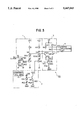
- a signal level converting circuit 10 comprises basically a level-shift circuit 1, a reference voltage circuit 2 and a differential circuit 3.
- the level-shift circuit 1 includes a first input terminal N1 supplied with an analog R (red), G (green) or B (blue) signal S-RGB.
- This terminal N1 is connected to the ground terminal through an input resistor R11 and further to the base of a PNP transistor Q11 which has a collector connected to the ground terminal and an emitter connected through a resistor R12 and a current source I11 to a power voltage line Vcc.
- the level-shift circuit 1 further includes a second input terminal N3 connected to the base of a PNP transistor Q12 having a collector connected to the ground terminal and an emitter connected through a resistor R13 and a current source I12 to the power voltage line Vcc.
- the resistors R12 and R13 have the same resistance value as each other.
- the connection point of the resistor R12 and the current source I11 and that of the resistor R13 and the current source I12 are led out first and second output nodes N2 and N4 of the circuit 1.
- the reference voltage circuit 2 includes a constant voltage generator 21 generating a constant voltage whose level corresponds to the white level of the input signal S-RGB. This voltage is supplied to a series connection circuit composed of a variable resistor R21, a diode D21 and a variable resistor R22. The connection point of the resistor R21 and the diode D21 is connected to the base of an NPN transistor Q21 which has a collector connected to the power voltage line Vcc and an emitter connected through a resistor R23 to the ground terminal. The transistor Q21 generates at its emitter a reference voltage VN3 which is in turn supplied to the second input node N3 of the level-shift circuit 2.
- the differential circuit 3 includes NPN transistors Q31 and Q32 having bases connected respectively to the output nodes N2 and N4 of the level-shift circuit 1.
- the transistors Q31 and Q32 are connected in a differential form through respective emitter resistors R31 and R32 to a current source composed of an NPN transistor Q33 and a resistor R35.
- the resistors R31 and R32 have the same resistance values as each other.
- the transistor Q33 is biased by a constant voltage Vcs to produce a constant current.
- the transistors Q31 and Q32 further have as a load resistor respective collector resistors R33 and R34 connected to a constant bias line VR and having the same resistance values as each other.
- the collectors of the transistors Q31 and Q32 serve as first and second output terminals N5 and N6, respectively, from which true and complementary level-shifted signals Vot and Voc are derived as output signals and then supplied to a signal processing circuit 4. If desired, only one of the output signals Vot and Voc may be led out and then supplied to the circuit 4.
- the analog RGB signal S-RGB as shown by VN1 in FIG. 3 is supplied to the input node N1 by using the resistor R11 as a termination resistor and then transferred to the base of the transistor Q11.
- the transistor Q12 receives at its base the reference voltage VN3 from the reference voltage circuit 2.
- the reference voltage VN3 has such a level that is a center level of the amplitude of the signal S-RGB by adjusting the values of the resistors R21 and R22, as shown in FIG. 3. Since the diode D21 has the same forward voltage drop as the base-emitter voltage of the transistor Q21, the reference voltage VN3 is stabilized against change in temperature.
- the signal appearing at the base of the transistor Q11 is thereby level-shifted so that the signal at the node N2 has a voltage level that is higher than the signal level S-RGB by the base-emitter voltage of the transistor Q11 and the voltage drop across the resistor R12, as denoted in FIG. 3 by the reference numeral VN2.
- the voltage drop across the resistor R12 is determined by the resistance value thereof and the constant current of the current source I11.
- the reference voltage Vn3 at the node N3 is level-shifted so that the voltage at the node N4 has the voltage level that is higher than the reference level VN 3 by the base-emitter voltage of the transistor and the voltage drop across the resistor R13, as shown in FIG. 3 by the reference numeral VN4.
- the voltage drop across the resistor R13 is determined by the resistance value thereof and the constant current of the current source I12. Since the current produced by the current source I11 is designed to be the same value as the current from the source I12, the level-shifted reference voltage VN4 takes the center level of the amplitude of the level-shifted signal VN2, as shown in FIG. 3.
- the differential circuit 3 thus receives the level-shifted signal VN2 and the level-shifted reference voltage VN4 at the bases of the transistors Q31 and Q32, respectively.
- the amplification gain of the differential circuit 3 is nearly equal to the ratio of the resistance value of the resistor R33 (or R34) to the sum of the resistance values of the resistors R31 and R32.
- the dc bias voltage of the output terminal N5 is equal to that of the output terminal N6 and is determined by the voltage of the bias line VR, the resistance value of the resistor R33 (or R34) and a half of the current produced by the transistor Q33.
- the dc bias voltage of each of the output terminals N5 and N6 is represented in FIG. 3 by "VOBIAS".
- the output signal Vot generated by the present signal level converting circuit 10 as a level-shifted signal has a dc bias voltage denoted by VOBIAS and an amplitude obtained by the product of the above mentioned gain and the difference between the signal voltage VN2 and the reference voltage VN4, as shown in FIG. 3.
- the complementary output signal Voc has an phase opposite to the true signal Vot.
- the dc bias voltage VOBIAS of the output signal Vot (Voc) is determined by the differential circuit 3 itself and is easily designed to comply with the voltage required by the processing circuit 4.
- the input voltage supplied to the differential circuit 3 is obtained by the level-shift circuit 1 having two parts for the input signal S-RGB and the reference voltage VN3, and these parts have the same circuit constructions as each other. Therefore, the deviation from the designed value is equal in each part. That is, the level-shifting amount is equal between the voltage levels VN2 and VN4 irrespective of the deviation in values and/or characteristics among the resistors and transistors.
- the present circuit 10 has no feedback loop and thus operates with a quick response to process a high frequency signal S-RGB.
- FIG. 4 there is shown a signal converting circuit 20 according to a second embodiment of the present invention, in which the same constituents as those shown in FIG. 2 are denoted by the same reference numerals to omit the further description thereof.
- diode chains DD11 and DD12 are employed in place of the resistors R12 and R13 shown in FIG. 1, respectively.
- One or more diodes may be used as each of the diode chains DD11 and DD12. Since the diode chains are employed, the response speed is further improved even when each of the current sources I11 and I12 has a certain stray capacitance.
- the input signal S-RGB may be changed in amplitude dependently of a system or equipment to which the present circuit is applied.
- the reference voltage circuit 2 is required to adjust its output reference voltage VN 3 to take a center level of the input signal S-RGB. It is therefore preferable to construct a circuit such that the amplitude of the input signal is also adjustable.
- FIG. 5 A circuit construction for that purpose is shown in FIG. 5 as a third embodiment of the present invention, in which the same constituents as those shown in FIG. 4 are denoted by the same reference numerals to omit the further description thereof.
- two N-channel MOS transistors M11 and M12 are connected in series between the input terminal N1 and the ground terminal in parallel to the resistor R11.
- the connection point N1A is connected to the base of the transistor Q11.
- the gates of the transistors M11 and M12 are supplied with bias voltage VATH and VATL, respectively. Accordingly, the impedances of the transistors M11 and M12 are controlled by the bias voltages VATH and VATL to adjust the amplitude of the signal S-RGB. Since the MOS transistor is of a bidirectional element, the linearity thereof is as good as a resistor with presenting a required resistance value by occupying area in a semiconductor chip smaller than a resistor.
Landscapes
- Engineering & Computer Science (AREA)
- Theoretical Computer Science (AREA)
- Signal Processing (AREA)
- Crystallography & Structural Chemistry (AREA)
- Computer Hardware Design (AREA)
- General Physics & Mathematics (AREA)
- Chemical & Material Sciences (AREA)
- Multimedia (AREA)
- Physics & Mathematics (AREA)
- Amplifiers (AREA)
- Liquid Crystal Display Device Control (AREA)
- Transforming Electric Information Into Light Information (AREA)
- Video Image Reproduction Devices For Color Tv Systems (AREA)
- Controls And Circuits For Display Device (AREA)
- Logic Circuits (AREA)
Applications Claiming Priority (2)
| Application Number | Priority Date | Filing Date | Title |
|---|---|---|---|
| JP5014380A JP2586785B2 (ja) | 1993-02-01 | 1993-02-01 | 信号レベル変換回路 |
| JP5-014380 | 1993-02-01 |
Publications (1)
| Publication Number | Publication Date |
|---|---|
| US5467043A true US5467043A (en) | 1995-11-14 |
Family
ID=11859444
Family Applications (1)
| Application Number | Title | Priority Date | Filing Date |
|---|---|---|---|
| US08/189,743 Expired - Lifetime US5467043A (en) | 1993-02-01 | 1994-02-01 | Signal level converting circuit for liquid crystal display device receiving analog color signal |
Country Status (4)
| Country | Link |
|---|---|
| US (1) | US5467043A (ja) |
| EP (1) | EP0609844A3 (ja) |
| JP (1) | JP2586785B2 (ja) |
| KR (1) | KR0120954B1 (ja) |
Cited By (6)
| Publication number | Priority date | Publication date | Assignee | Title |
|---|---|---|---|---|
| US5764094A (en) * | 1995-06-02 | 1998-06-09 | Matsushita Electric Industrial Co., Ltd. | Level shift circuit for analog signal and signal waveform generator including the same |
| US6157361A (en) * | 1996-07-22 | 2000-12-05 | Sharp Kabushiki Kaisha | Matrix-type image display device |
| US6384808B2 (en) | 2000-03-14 | 2002-05-07 | Semiconductor Energy Laboratory Co., Ltd | Level shifter |
| US20020140660A1 (en) * | 1998-06-23 | 2002-10-03 | Hideo Sato | Liquid crystal display apparatus having level conversion circuit |
| US20050242669A1 (en) * | 2004-04-30 | 2005-11-03 | Fattaruso John W | Apparatus and method for shifting a signal from a first reference level to a second reference level |
| US20070296660A1 (en) * | 2006-06-02 | 2007-12-27 | Semiconductor Energy Laboratory Co., Ltd. | Semiconductor device and electronic apparatus having the same |
Families Citing this family (2)
| Publication number | Priority date | Publication date | Assignee | Title |
|---|---|---|---|---|
| JP2000056330A (ja) * | 1998-08-06 | 2000-02-25 | Sony Corp | 液晶表示装置 |
| KR100835518B1 (ko) * | 2001-12-20 | 2008-06-04 | 엘지디스플레이 주식회사 | 레벨 쉬프트 회로 |
Citations (15)
| Publication number | Priority date | Publication date | Assignee | Title |
|---|---|---|---|---|
| US3956661A (en) * | 1973-11-20 | 1976-05-11 | Tokyo Sanyo Electric Co., Ltd. | D.C. power source with temperature compensation |
| US3959666A (en) * | 1974-07-01 | 1976-05-25 | Honeywell Information Systems, Inc. | Logic level translator |
| US4119869A (en) * | 1976-02-26 | 1978-10-10 | Tokyo Shibaura Electric Company, Ltd. | Constant current circuit |
| US4366397A (en) * | 1979-06-29 | 1982-12-28 | Hitachi, Ltd. | Level conversion circuit |
| US4401901A (en) * | 1981-06-01 | 1983-08-30 | Advanced Micro Devices, Inc. | Comparator |
| US4456840A (en) * | 1980-12-26 | 1984-06-26 | Fujitsu Limited | Comparator circuit |
| US4675555A (en) * | 1984-12-28 | 1987-06-23 | Fujitsu Limited | IC input buffer emitter follower with current source value dependent upon connection length for equalizing signal delay |
| US4791312A (en) * | 1987-06-08 | 1988-12-13 | Grumman Aerospace Corporation | Programmable level shifting interface device |
| US4810908A (en) * | 1986-12-01 | 1989-03-07 | Hirokazu Suzuki | Semiconductor logic circuit comprising clock driver and clocked logic circuit |
| US4945258A (en) * | 1988-12-08 | 1990-07-31 | Grumman Aerospace Corporation | Monolithic gaAs high speed switch driver |
| US4994691A (en) * | 1990-04-16 | 1991-02-19 | Advanced Micro Devices, Inc. | TTL-to-CML translator circuit |
| EP0436384A2 (en) * | 1989-12-27 | 1991-07-10 | Sharp Kabushiki Kaisha | A driving circuit for a liquid crystal display apparatus |
| EP0501085A1 (en) * | 1991-02-28 | 1992-09-02 | International Business Machines Corporation | Level-shifter circuit for high-speed low-power biCMOS ECL to CMOS input buffers |
| US5237220A (en) * | 1991-02-06 | 1993-08-17 | Nec Corporation | Master-slice type ECL circuit |
| US5296760A (en) * | 1992-07-20 | 1994-03-22 | Motorola, Inc. | Voltage translator |
Family Cites Families (1)
| Publication number | Priority date | Publication date | Assignee | Title |
|---|---|---|---|---|
| JPS62218943A (ja) * | 1986-03-19 | 1987-09-26 | Sharp Corp | 液晶表示装置 |
-
1993
- 1993-02-01 JP JP5014380A patent/JP2586785B2/ja not_active Expired - Fee Related
-
1994
- 1994-01-31 KR KR1019940001734A patent/KR0120954B1/ko active IP Right Grant
- 1994-02-01 EP EP94101483A patent/EP0609844A3/en not_active Withdrawn
- 1994-02-01 US US08/189,743 patent/US5467043A/en not_active Expired - Lifetime
Patent Citations (15)
| Publication number | Priority date | Publication date | Assignee | Title |
|---|---|---|---|---|
| US3956661A (en) * | 1973-11-20 | 1976-05-11 | Tokyo Sanyo Electric Co., Ltd. | D.C. power source with temperature compensation |
| US3959666A (en) * | 1974-07-01 | 1976-05-25 | Honeywell Information Systems, Inc. | Logic level translator |
| US4119869A (en) * | 1976-02-26 | 1978-10-10 | Tokyo Shibaura Electric Company, Ltd. | Constant current circuit |
| US4366397A (en) * | 1979-06-29 | 1982-12-28 | Hitachi, Ltd. | Level conversion circuit |
| US4456840A (en) * | 1980-12-26 | 1984-06-26 | Fujitsu Limited | Comparator circuit |
| US4401901A (en) * | 1981-06-01 | 1983-08-30 | Advanced Micro Devices, Inc. | Comparator |
| US4675555A (en) * | 1984-12-28 | 1987-06-23 | Fujitsu Limited | IC input buffer emitter follower with current source value dependent upon connection length for equalizing signal delay |
| US4810908A (en) * | 1986-12-01 | 1989-03-07 | Hirokazu Suzuki | Semiconductor logic circuit comprising clock driver and clocked logic circuit |
| US4791312A (en) * | 1987-06-08 | 1988-12-13 | Grumman Aerospace Corporation | Programmable level shifting interface device |
| US4945258A (en) * | 1988-12-08 | 1990-07-31 | Grumman Aerospace Corporation | Monolithic gaAs high speed switch driver |
| EP0436384A2 (en) * | 1989-12-27 | 1991-07-10 | Sharp Kabushiki Kaisha | A driving circuit for a liquid crystal display apparatus |
| US4994691A (en) * | 1990-04-16 | 1991-02-19 | Advanced Micro Devices, Inc. | TTL-to-CML translator circuit |
| US5237220A (en) * | 1991-02-06 | 1993-08-17 | Nec Corporation | Master-slice type ECL circuit |
| EP0501085A1 (en) * | 1991-02-28 | 1992-09-02 | International Business Machines Corporation | Level-shifter circuit for high-speed low-power biCMOS ECL to CMOS input buffers |
| US5296760A (en) * | 1992-07-20 | 1994-03-22 | Motorola, Inc. | Voltage translator |
Non-Patent Citations (2)
| Title |
|---|
| Patent Abstracts of Japan, vol. 12, No. 86, 18 Mar. 1988. * |
| Sedra & Smith, Microelectronic Circuits, Saunders College Publishing, Philadelphia, 1991. * |
Cited By (21)
| Publication number | Priority date | Publication date | Assignee | Title |
|---|---|---|---|---|
| US5764094A (en) * | 1995-06-02 | 1998-06-09 | Matsushita Electric Industrial Co., Ltd. | Level shift circuit for analog signal and signal waveform generator including the same |
| US6157361A (en) * | 1996-07-22 | 2000-12-05 | Sharp Kabushiki Kaisha | Matrix-type image display device |
| US6373460B1 (en) | 1996-07-22 | 2002-04-16 | Sharp Kabushiki Kaisha | Matrix-type image display device having level shifters |
| US6919873B2 (en) | 1998-06-23 | 2005-07-19 | Hitachi, Ltd. | Liquid crystal display apparatus having level conversion circuit |
| US7460100B2 (en) | 1998-06-23 | 2008-12-02 | Hitachi, Ltd. | Liquid crystal display apparatus having level conversion circuit |
| US20020140660A1 (en) * | 1998-06-23 | 2002-10-03 | Hideo Sato | Liquid crystal display apparatus having level conversion circuit |
| US6714184B2 (en) * | 1998-06-23 | 2004-03-30 | Hitachi, Ltd. | Liquid crystal display apparatus having level conversion circuit |
| US20040196249A1 (en) * | 1998-06-23 | 2004-10-07 | Hideo Sato | Liquid crystal display apparatus having level conversion circuit |
| CN100344062C (zh) * | 2000-03-14 | 2007-10-17 | 株式会社半导体能源研究所 | 电平移动器 |
| US6567067B2 (en) | 2000-03-14 | 2003-05-20 | Semiconductor Energy Laboratory Co., Ltd. | Level shifter |
| US6384808B2 (en) | 2000-03-14 | 2002-05-07 | Semiconductor Energy Laboratory Co., Ltd | Level shifter |
| US20050242669A1 (en) * | 2004-04-30 | 2005-11-03 | Fattaruso John W | Apparatus and method for shifting a signal from a first reference level to a second reference level |
| US7535280B2 (en) * | 2004-04-30 | 2009-05-19 | Texas Instruments Incorporated | Apparatus and method for shifting a signal from a first reference level to a second reference level |
| US20070296660A1 (en) * | 2006-06-02 | 2007-12-27 | Semiconductor Energy Laboratory Co., Ltd. | Semiconductor device and electronic apparatus having the same |
| US7443202B2 (en) | 2006-06-02 | 2008-10-28 | Semiconductor Energy Laboratory Co., Ltd. | Semiconductor device and electronic apparatus having the same |
| US20090027083A1 (en) * | 2006-06-02 | 2009-01-29 | Semiconductor Energy Laboratory Co., Ltd. | Semiconductor device and electronic apparatus having the same |
| US7663404B2 (en) | 2006-06-02 | 2010-02-16 | Semiconductor Energy Laboratory Co., Ltd. | Semiconductor device and electronic apparatus having the same |
| US20100134708A1 (en) * | 2006-06-02 | 2010-06-03 | Semiconductor Energy Laboratory Co., Ltd. | Semiconductor device and electronic apparatus having the same |
| US7961006B2 (en) | 2006-06-02 | 2011-06-14 | Semiconductor Energy Laboratory Co., Ltd. | Semiconductor device and electronic apparatus having the same |
| US20110233633A1 (en) * | 2006-06-02 | 2011-09-29 | Semiconductor Energy Laboratory Co., Ltd. | Semiconductor Device and Electronic Apparatus Having the Same |
| US8471596B2 (en) | 2006-06-02 | 2013-06-25 | Semiconductor Energy Laboratory Co., Ltd. | Semiconductor device and electronic apparatus having the same |
Also Published As
| Publication number | Publication date |
|---|---|
| EP0609844A2 (en) | 1994-08-10 |
| KR0120954B1 (ko) | 1997-10-22 |
| KR940020151A (ko) | 1994-09-15 |
| JPH06230740A (ja) | 1994-08-19 |
| JP2586785B2 (ja) | 1997-03-05 |
| EP0609844A3 (en) | 1995-03-29 |
Similar Documents
| Publication | Publication Date | Title |
|---|---|---|
| US5467043A (en) | Signal level converting circuit for liquid crystal display device receiving analog color signal | |
| US7113041B2 (en) | Operational amplifier | |
| US5081378A (en) | Logarithmic amplifier | |
| US4007427A (en) | Cascaded transistor amplifier stages | |
| US6114874A (en) | Complementary MOS level translating apparatus and method | |
| US6104232A (en) | DC output level compensation circuit | |
| US6064268A (en) | Precision emitter follower | |
| US6724234B1 (en) | Signal-level compensation for communications circuits | |
| US4477780A (en) | Operational amplifier with multiple switchable outputs | |
| US6396319B2 (en) | Semiconductor integrated circuit with quick charging/discharging circuit | |
| US5963065A (en) | Low offset push-pull amplifier | |
| CA1205149A (en) | Integrated video amp with common base lateral pnp transistor | |
| US5606271A (en) | Extreme level circuit | |
| US7279976B1 (en) | Differential amplifier with controlled common mode output voltage | |
| US5815011A (en) | Circuit for adjusting the coring threshold of a signal | |
| JPH07274039A (ja) | 画像信号補正器及び信号変換器 | |
| JP3358747B2 (ja) | 映像出力装置 | |
| JPH0983341A (ja) | レベル変換回路 | |
| JPH04354408A (ja) | 電流極性変換回路 | |
| JPH04273707A (ja) | レベルシフト回路 | |
| JPH07154167A (ja) | エミッタホロワ出力電流制限回路 | |
| JPS62101108A (ja) | ボルテ−ジ・フオロワ | |
| JP2002176322A (ja) | レベルシフト回路付き増幅回路 | |
| JPH1041752A (ja) | 電力増幅器 | |
| JPH0659013B2 (ja) | 出力増幅回路 |
Legal Events
| Date | Code | Title | Description |
|---|---|---|---|
| AS | Assignment |
Owner name: NEC CORPORATION, JAPAN Free format text: ASSIGNMENT OF ASSIGNORS INTEREST;ASSIGNOR:OHI, SUSUMU;REEL/FRAME:006860/0772 Effective date: 19940125 |
|
| STCF | Information on status: patent grant |
Free format text: PATENTED CASE |
|
| FEPP | Fee payment procedure |
Free format text: PAYOR NUMBER ASSIGNED (ORIGINAL EVENT CODE: ASPN); ENTITY STATUS OF PATENT OWNER: LARGE ENTITY |
|
| FPAY | Fee payment |
Year of fee payment: 4 |
|
| FPAY | Fee payment |
Year of fee payment: 8 |
|
| AS | Assignment |
Owner name: NEC LCD TECHNOLOGIES, LTD., JAPAN Free format text: ASSIGNMENT OF ASSIGNORS INTEREST;ASSIGNOR:NEC CORPORATION;REEL/FRAME:014108/0248 Effective date: 20030401 |
|
| FPAY | Fee payment |
Year of fee payment: 12 |
|
| AS | Assignment |
Owner name: NLT TECHNOLOGIES, LTD., JAPAN Free format text: CHANGE OF NAME;ASSIGNOR:NEC LCD TECHNOLOGIES, LTD.;REEL/FRAME:027188/0698 Effective date: 20110701 |