US5350492A - Oxide removal method for improvement of subsequently grown oxides - Google Patents
Oxide removal method for improvement of subsequently grown oxides Download PDFInfo
- Publication number
- US5350492A US5350492A US07/947,314 US94731492A US5350492A US 5350492 A US5350492 A US 5350492A US 94731492 A US94731492 A US 94731492A US 5350492 A US5350492 A US 5350492A
- Authority
- US
- United States
- Prior art keywords
- oxide
- dielectric
- etching
- thick oxide
- thin
- Prior art date
- Legal status (The legal status is an assumption and is not a legal conclusion. Google has not performed a legal analysis and makes no representation as to the accuracy of the status listed.)
- Expired - Lifetime
Links
Images


Classifications
-
- H—ELECTRICITY
- H01—ELECTRIC ELEMENTS
- H01L—SEMICONDUCTOR DEVICES NOT COVERED BY CLASS H10
- H01L21/00—Processes or apparatus adapted for the manufacture or treatment of semiconductor or solid state devices or of parts thereof
- H01L21/70—Manufacture or treatment of devices consisting of a plurality of solid state components formed in or on a common substrate or of parts thereof; Manufacture of integrated circuit devices or of parts thereof
- H01L21/71—Manufacture of specific parts of devices defined in group H01L21/70
- H01L21/76—Making of isolation regions between components
- H01L21/762—Dielectric regions, e.g. EPIC dielectric isolation, LOCOS; Trench refilling techniques, SOI technology, use of channel stoppers
- H01L21/76202—Dielectric regions, e.g. EPIC dielectric isolation, LOCOS; Trench refilling techniques, SOI technology, use of channel stoppers using a local oxidation of silicon, e.g. LOCOS, SWAMI, SILO
-
- H—ELECTRICITY
- H01—ELECTRIC ELEMENTS
- H01L—SEMICONDUCTOR DEVICES NOT COVERED BY CLASS H10
- H01L21/00—Processes or apparatus adapted for the manufacture or treatment of semiconductor or solid state devices or of parts thereof
- H01L21/02—Manufacture or treatment of semiconductor devices or of parts thereof
- H01L21/04—Manufacture or treatment of semiconductor devices or of parts thereof the devices having at least one potential-jump barrier or surface barrier, e.g. PN junction, depletion layer or carrier concentration layer
- H01L21/18—Manufacture or treatment of semiconductor devices or of parts thereof the devices having at least one potential-jump barrier or surface barrier, e.g. PN junction, depletion layer or carrier concentration layer the devices having semiconductor bodies comprising elements of Group IV of the Periodic System or AIIIBV compounds with or without impurities, e.g. doping materials
- H01L21/30—Treatment of semiconductor bodies using processes or apparatus not provided for in groups H01L21/20 - H01L21/26
- H01L21/31—Treatment of semiconductor bodies using processes or apparatus not provided for in groups H01L21/20 - H01L21/26 to form insulating layers thereon, e.g. for masking or by using photolithographic techniques; After treatment of these layers; Selection of materials for these layers
- H01L21/3105—After-treatment
- H01L21/311—Etching the insulating layers by chemical or physical means
- H01L21/31105—Etching inorganic layers
- H01L21/31111—Etching inorganic layers by chemical means
-
- Y—GENERAL TAGGING OF NEW TECHNOLOGICAL DEVELOPMENTS; GENERAL TAGGING OF CROSS-SECTIONAL TECHNOLOGIES SPANNING OVER SEVERAL SECTIONS OF THE IPC; TECHNICAL SUBJECTS COVERED BY FORMER USPC CROSS-REFERENCE ART COLLECTIONS [XRACs] AND DIGESTS
- Y10—TECHNICAL SUBJECTS COVERED BY FORMER USPC
- Y10S—TECHNICAL SUBJECTS COVERED BY FORMER USPC CROSS-REFERENCE ART COLLECTIONS [XRACs] AND DIGESTS
- Y10S438/00—Semiconductor device manufacturing: process
- Y10S438/911—Differential oxidation and etching
Definitions
- This invention relates to the fabrication of semiconductor devices, and more specifically, to the removal of oxides from the surface of a semiconductor substrate.
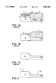
- FIGS. 1A, 1B, and 1C are cross sections of a portion of a CMOS structure which illustrate several steps in the removal of the N-well oxide grown during the drive-in of an N-well implant.
- FIG. 1A shows the structure immediately after the N-well oxidation.
- N-well oxide 14 is nominally 2700 ⁇ thick, having been grown to this thickness by a previous high temperature drive-in step for diffusing and activating the N-well implant (not shown) to form N-well 22. This specific thickness of 2700 ⁇ also provides a useful layer thickness to devise alignment structures for certain lithographic equipment.
- Nitride 10 covers the P-well 20 to prevent the implantation of the n-type dopant into the P-well 20, as well as to prevent the growth of any subsequent oxide over the P-well 20 during the formation of oxide layer 14 over the N-well 22.
- Nitride layer 10 is typically 920 ⁇ thick.
- the nitride layer 10 over the P-well 20 is next removed with a wet phosphoric acid strip. Because of the extremely high selectivity of phosphoric acid between nitride and oxide, very little oxide is removed during this etch step. Barrier oxide 12 covers the P-well 20 and provides an etch-stop barrier during this nitride removal process, as the phosphoric acid used to etch the nitride 10 would also etch the silicon substrate itself in the P-well 20. This barrier oxide 12 is approximately 400 ⁇ thick. The structure remaining after nitride 10 removal is shown in FIG. 1B. As very little oxide was removed by the nitride etch step, the nominal thickness of barrier oxide 12 is still 400 ⁇ , and the nominal thickness of N-well oxide 14 remains at 2700 ⁇ .
- the next step is a 12 minute 10:1 HF dip etch which is required to remove the 2700 ⁇ of N-well oxide 14.
- the resulting structure following the HF dip etch is shown in FIG. 1C.
- the surface is subject to an RCA clean, and a thin oxide is subsequently grown over the exposed surface of the semiconductor material.
- This thin oxide may be a tunnel oxide or a gate oxide, for example.
- the present invention advantageously avoids excessively over-etching surface portions of a semiconductor body in the removal by etching of dielectrics of different thicknesses from these surface portions.
- the avoidance of over-etching facilitates the making of high quality thin oxides for numerous semiconductor fabrication purposes, including the making of tunnel oxides in the fabrication of EEPROM devices.
- the present invention involves converting a thick dielectric into a dielectric of thickness comparable to a thin dielectric.
- a protective material is provided over the thin dielectric. Once the converting step is complete, the protective material is removed, and both the thin dielectric and converted dielectric are etched without appreciably over-etching the underlying semiconductor surfaces.
- the converting step involves etching the thick dielectric, which is an oxide formed during a drive-in fabrication step, down to a thickness comparable to the thickness of the thin dielectric, which is a barrier oxide provided between a nitride layer and the silicon substrate. The nitride layer also acts as the protective material.
- FIGS. 1A, 1B, and 1C are cross-sectional views illustrating a prior-art process flow for removing oxides of different thickness in a CMOS process.
- FIG. 2 is a cross-sectional view illustrating the actual surface resulting from the oxide etch step of the structure shown in FIG. 1B.
- FIGS. 3A, 3B, 3C, and 3D are cross-sectional views illustrating a process flow, in accordance with the present invention, for removing oxides of different thickness in a CMOS process.
- FIG. 4 is a histogram of Edge QBD measurements for the structures resulting from the process flows of FIGS. 1A, 1B and 1C and FIGS. 3A, 3B, 3C and 3D.
- FIG. 5 is a histogram of Surface QBD measurements for the structures resulting from the process flows of FIGS. 1A, 1B and 1C and FIGS. 3A, 3B, 3C and 3D.
- the etch rate of silicon dioxide in 10:1 HF is nominally 325 ⁇ /minute
- the 2700 ⁇ thick N-well oxide 14 requires a 12 minute etch (which allows for manufacturing variations in exact thickness and etch rates).
- the barrier oxide 12 is only 400 ⁇ thick, the silicon substrate over the P-well 20 unfortunately receives an over-etch of 10.75 minutes, representing an over-etch of 860%.
- FIG. 2 shows the surfaces 16 (over the P-well 20) and 18 (over the N-well 22) actually resulting from the oxide etch of the structure shown in FIG. 1B.
- P-well surface 16 shows micro-roughness, due to the tremendous over-etch experienced by this surface 16.
- N-well surface 18 is free from significant over-etch effects, since the etch was timed for complete removal of the N-well oxide 14, with only the customary nominal over-etch (to assure complete removal of the N-well oxide 14).
- FIGS. 3A to 3D are cross-sections of a portion of a CMOS structure at various steps in a process which reduces substantially the amount of over-etch of the P-well surface, thereby improving the quality of subsequently grown thin oxides.
- the practical implication of the process used to form the structures of FIGS. 3B to 3D is the improvement of manufacturing yields and product quality.
- FIG. 3A which is identical to FIG. 1A, shows in cross-section a portion of a device structure immediately after N-well oxidation.
- N-well oxide 14 is nominally 2700 ⁇ thick, having been grown to this thickness by a previous high temperature drive-in step for diffusing and activating the N-well implant (not shown) to form N-well 22.
- Nitride 10 covers the P-well 20 to prevent the implantation of the n-type dopant into the P-well 20, as well as to prevent the growth of any subsequent oxide over the P-well 20 during the N-well oxidation.
- Nitride layer 10 is typically 920 ⁇ thick.
- N-well oxide 14 is now removed. This is accomplished by a 6 minute 10:1 HF dip etch that removes approximately 2000 ⁇ of the N-well oxide 14. The resulting structure is shown in FIG. 3B. The remaining N-well oxide 115 is approximately 700 ⁇ thick.
- the nitride layer 10 over the P-well 20 is removed with a wet phosphoric acid strip.
- Barrier oxide 12 covers the P-well 20, and remaining N-well oxide 115 covers the N-well 22, as both provide an etch stop during the nitride removal. Because of the extremely high selectivity of phosphoric acid between nitride and oxide, very little oxide is removed during this etch step.
- the resulting structure remaining after nitride removal is shown in FIG. 3C.
- the nominal thickness of barrier oxide 12 is still 400 ⁇ , and the nominal thickness of remaining N-well oxide 115 is 700 ⁇ .
- a 3 minute 10:1 HF dip is performed to remove the barrier oxide 12 and the remaining N-well oxide 115. Since the thicknesses of the two oxides are comparable, an etch step sufficient to remove the thicker oxide will not subject the surface beneath the thinner oxide to substantial over-etching.
- the barrier oxide 12 is subjected to a total etch time of 3 minutes, rather than 12 minutes as in the process of FIGS. 1A to 1C, which reduces the over-etch from 860% to only 144%. Naturally, the over-etch time can be further reduced by reducing the thickness of remaining N-well oxide 115 to be closer to, or even less than, the thickness of barrier oxide 12.
- FIG. 3D shows the resulting structure remaining after the above mentioned oxide etch step.
- P-well surface 116 shows much less micro-roughness, due to the significantly reduced amount of over-etch experienced by this surface.
- the structure shown in FIG. 3D typically is subject to an RCA clean prior to subsequent oxide growth. If care is taken, the RCA clean will not appreciably damage the P-well surface 116 and N-well surface 18. Suitable RCA clean techniques are described in "Dependence of Thin Oxide Quality on Surface Micro-Roughness" by T. Ohmi, et. al., IEEE Transactions on Electron Devices, Vol. 39, Number 3, March 1992.
- the thicker oxides are converted to oxides having thickness comparable to the thickness of the thin oxide.
- none of these surface regions is subject to greater than about a two minute over-etch time.
- barrier oxide 12 typically is in the range of 150-500 ⁇ thick and N-well oxide 14 typically is as thick as 6000 ⁇ , conversion of the oxide 14 to an oxide 115 of, for example, less than about 1000 ⁇ allows for a suitably limited over-etch in the subsequent oxide etch step.
- Tunnel oxides for, illustratively, an EEPROM technology were grown to provide a sub-100 ⁇ oxide for oxide quality measurements. Quality improvements achieved for this type of oxide can be equally applied to a wide variety of semiconductor devices. Silicon-gate transistors were also fabricated in both the N-well and the P-well to ascertain any effects upon device characteristics.
- QBD charge-to-breakdown
- charge-to-breakdown is a measure of the time-dependent breakdown characteristic of an oxide layer. It is measured by passing a constant current through the oxide under test (which conducts via Fowler-Nordheim tunneling), and noting the time at which the oxide breaks down electrically. Breakdown occurs due to the trapping of charge within the oxide, thereby gradually raising the electric field across the oxide until the oxide can no longer withstand the induced voltage. Higher quality oxides will trap less charge over time, and will therefore take longer to break down.
- the mathematical product of the forcing current times the measured time to breakdown gives rise to a charge value corresponding to the total charge passed through the oxide prior to breakdown. Higher QBD values reflect higher quality oxides.
- FIG. 4 shows a histogram of measurements for the Edge QBD structure, for both the process flow of FIGS. 1A to 1C and the process flow of FIGS. 3A to 3D.
- 16% of the wafers from the process flow of FIGS. 1A to 1C (bar 200) produced a zero value for this test, indicating an initial electrical short in the oxide layer with minimal applied voltage.
- the group of wafers from the process flow of FIGS. 3A to 3D had no shorted wafers.
- the mean value of edge QBD improves from 3.15 to 3.73 coul/cm**2, for a 20% improvement.
- the sigma of the distributions was also enhanced by a factor of 3.5, representing much better uniformity of the grown oxides.
- FIGS. 3A to 3D yields a higher quality oxide, at lower cost, while producing no known unwanted side effects in N-channel and P-channel transistor characteristics.
- the invention has been described with respect to the embodiments set forth above, the invention is not necessarily limited to these embodiments.
- the invention is not necessarily limited to any particular transistor process technology, or to any particular layer thickness or composition.
- variations in certain of the process steps can be practiced.
- conversion of the thick N-well oxide 14 may be achieved by removing the oxide 14 entirely and growing a new oxide to the thickness of the N-well oxide feature 115. Accordingly, other embodiments, variations, and improvements not described herein are not necessarily excluded from the scope of the invention, which is defined by the following claims.
Priority Applications (4)
| Application Number | Priority Date | Filing Date | Title |
|---|---|---|---|
| US07/947,314 US5350492A (en) | 1992-09-18 | 1992-09-18 | Oxide removal method for improvement of subsequently grown oxides |
| EP93305167A EP0592071B1 (en) | 1992-09-18 | 1993-07-01 | A dielectric removal method |
| DE69332496T DE69332496T2 (de) | 1992-09-18 | 1993-07-01 | Verfahren zur Dielektrikim-Entfernung |
| JP5220946A JPH06204203A (ja) | 1992-09-18 | 1993-09-06 | 半導体本体の表面から誘電体を除去する方法および半導体本体の表面から酸化物を除去する方法ならびに半導体本体の表面の劣化を回避する方法 |
Applications Claiming Priority (1)
| Application Number | Priority Date | Filing Date | Title |
|---|---|---|---|
| US07/947,314 US5350492A (en) | 1992-09-18 | 1992-09-18 | Oxide removal method for improvement of subsequently grown oxides |
Publications (1)
| Publication Number | Publication Date |
|---|---|
| US5350492A true US5350492A (en) | 1994-09-27 |
Family
ID=25485943
Family Applications (1)
| Application Number | Title | Priority Date | Filing Date |
|---|---|---|---|
| US07/947,314 Expired - Lifetime US5350492A (en) | 1992-09-18 | 1992-09-18 | Oxide removal method for improvement of subsequently grown oxides |
Country Status (4)
| Country | Link |
|---|---|
| US (1) | US5350492A (ja) |
| EP (1) | EP0592071B1 (ja) |
| JP (1) | JPH06204203A (ja) |
| DE (1) | DE69332496T2 (ja) |
Cited By (9)
| Publication number | Priority date | Publication date | Assignee | Title |
|---|---|---|---|---|
| US5529947A (en) * | 1993-12-15 | 1996-06-25 | Nec Corporation | Semiconductor device with clad substrate and fabrication process therefor |
| US5858843A (en) * | 1996-09-27 | 1999-01-12 | Intel Corporation | Low temperature method of forming gate electrode and gate dielectric |
| US5981402A (en) * | 1997-12-31 | 1999-11-09 | United Semiconductor Corp. | Method of fabricating shallow trench isolation |
| US6613677B1 (en) * | 1997-11-28 | 2003-09-02 | Arizona Board Of Regents | Long range ordered semiconductor interface phase and oxides |
| US20050231557A1 (en) * | 2004-04-14 | 2005-10-20 | Krawczyk John W | Micro-fluid ejection assemblies |
| US20100190345A1 (en) * | 2009-01-26 | 2010-07-29 | Neng-Kuo Chen | Selective Etch-Back Process for Semiconductor Devices |
| US9018077B2 (en) | 2009-04-30 | 2015-04-28 | Arizona Board Of Regents, A Body Corporate Of The State Of Arizona, Acting For And On Behalf Of Arizona State University | Methods for wafer bonding, and for nucleating bonding nanophases |
| US9418963B2 (en) | 2012-09-25 | 2016-08-16 | Arizona Board Of Regents, A Body Corporate Of The State Of Arizona Acting For And On Behalf Of Arizona State University | Methods for wafer bonding, and for nucleating bonding nanophases |
| US9589801B2 (en) | 2011-10-31 | 2017-03-07 | Arizona Board Of Regents, A Body Corporated Of The State Of Arizona, Acting For And On Behalf Of Arizona State University | Methods for wafer bonding and for nucleating bonding nanophases using wet and steam pressurization |
Families Citing this family (1)
| Publication number | Priority date | Publication date | Assignee | Title |
|---|---|---|---|---|
| CN110323134A (zh) * | 2019-07-11 | 2019-10-11 | 上海遂泰科技有限公司 | 一种功率器件的生产工艺方法 |
Citations (4)
| Publication number | Priority date | Publication date | Assignee | Title |
|---|---|---|---|---|
| US4472240A (en) * | 1981-08-21 | 1984-09-18 | Tokyo Shibaura Denki Kabushiki Kaisha | Method for manufacturing semiconductor device |
| US4713329A (en) * | 1985-07-22 | 1987-12-15 | Data General Corporation | Well mask for CMOS process |
| JPS632055A (ja) * | 1986-04-11 | 1988-01-07 | ゼロツクス コ−ポレ−シヨン | 有機アゾ光導電体像形成部材 |
| JPH0272661A (ja) * | 1988-09-07 | 1990-03-12 | Mitsubishi Electric Corp | 半導体装置の製造方法 |
Family Cites Families (2)
| Publication number | Priority date | Publication date | Assignee | Title |
|---|---|---|---|---|
| US4539744A (en) * | 1984-02-03 | 1985-09-10 | Fairchild Camera & Instrument Corporation | Semiconductor planarization process and structures made thereby |
| JPH088298B2 (ja) * | 1988-10-04 | 1996-01-29 | 沖電気工業株式会社 | 半導体素子の製造方法 |
-
1992
- 1992-09-18 US US07/947,314 patent/US5350492A/en not_active Expired - Lifetime
-
1993
- 1993-07-01 EP EP93305167A patent/EP0592071B1/en not_active Expired - Lifetime
- 1993-07-01 DE DE69332496T patent/DE69332496T2/de not_active Expired - Lifetime
- 1993-09-06 JP JP5220946A patent/JPH06204203A/ja active Pending
Patent Citations (4)
| Publication number | Priority date | Publication date | Assignee | Title |
|---|---|---|---|---|
| US4472240A (en) * | 1981-08-21 | 1984-09-18 | Tokyo Shibaura Denki Kabushiki Kaisha | Method for manufacturing semiconductor device |
| US4713329A (en) * | 1985-07-22 | 1987-12-15 | Data General Corporation | Well mask for CMOS process |
| JPS632055A (ja) * | 1986-04-11 | 1988-01-07 | ゼロツクス コ−ポレ−シヨン | 有機アゾ光導電体像形成部材 |
| JPH0272661A (ja) * | 1988-09-07 | 1990-03-12 | Mitsubishi Electric Corp | 半導体装置の製造方法 |
Non-Patent Citations (6)
| Title |
|---|
| Elliot, Integrated Circuit Fabrication Technology, 1989, McGraw Hill, pp. 59 61, 398, 399. * |
| Elliot, Integrated Circuit Fabrication Technology, 1989, McGraw-Hill, pp. 59-61, 398, 399. |
| Ghandhi, VLSI Fabrication Principles, Wiley & Sons, 1983, pp. 421 430. * |
| Ghandhi, VLSI Fabrication Principles, Wiley & Sons, 1983, pp. 421-430. |
| Sze, VLSI Technology, McGraw Hill, 1988, p. 197. * |
| Sze, VLSI Technology, McGraw-Hill, 1988, p. 197. |
Cited By (11)
| Publication number | Priority date | Publication date | Assignee | Title |
|---|---|---|---|---|
| US5529947A (en) * | 1993-12-15 | 1996-06-25 | Nec Corporation | Semiconductor device with clad substrate and fabrication process therefor |
| US5858843A (en) * | 1996-09-27 | 1999-01-12 | Intel Corporation | Low temperature method of forming gate electrode and gate dielectric |
| US6613677B1 (en) * | 1997-11-28 | 2003-09-02 | Arizona Board Of Regents | Long range ordered semiconductor interface phase and oxides |
| US5981402A (en) * | 1997-12-31 | 1999-11-09 | United Semiconductor Corp. | Method of fabricating shallow trench isolation |
| US20050231557A1 (en) * | 2004-04-14 | 2005-10-20 | Krawczyk John W | Micro-fluid ejection assemblies |
| US7273266B2 (en) | 2004-04-14 | 2007-09-25 | Lexmark International, Inc. | Micro-fluid ejection assemblies |
| US20100190345A1 (en) * | 2009-01-26 | 2010-07-29 | Neng-Kuo Chen | Selective Etch-Back Process for Semiconductor Devices |
| US9159808B2 (en) * | 2009-01-26 | 2015-10-13 | Taiwan Semiconductor Manufacturing Company, Ltd. | Selective etch-back process for semiconductor devices |
| US9018077B2 (en) | 2009-04-30 | 2015-04-28 | Arizona Board Of Regents, A Body Corporate Of The State Of Arizona, Acting For And On Behalf Of Arizona State University | Methods for wafer bonding, and for nucleating bonding nanophases |
| US9589801B2 (en) | 2011-10-31 | 2017-03-07 | Arizona Board Of Regents, A Body Corporated Of The State Of Arizona, Acting For And On Behalf Of Arizona State University | Methods for wafer bonding and for nucleating bonding nanophases using wet and steam pressurization |
| US9418963B2 (en) | 2012-09-25 | 2016-08-16 | Arizona Board Of Regents, A Body Corporate Of The State Of Arizona Acting For And On Behalf Of Arizona State University | Methods for wafer bonding, and for nucleating bonding nanophases |
Also Published As
| Publication number | Publication date |
|---|---|
| EP0592071B1 (en) | 2002-11-20 |
| JPH06204203A (ja) | 1994-07-22 |
| DE69332496T2 (de) | 2003-10-09 |
| EP0592071A2 (en) | 1994-04-13 |
| DE69332496D1 (de) | 2003-01-02 |
| EP0592071A3 (en) | 1997-10-08 |
Similar Documents
| Publication | Publication Date | Title |
|---|---|---|
| US5151381A (en) | Method for local oxidation of silicon employing two oxidation steps | |
| US5316981A (en) | Method for achieving a high quality thin oxide using a sacrificial oxide anneal | |
| US6165846A (en) | Method of eliminating gate leakage in nitrogen annealed oxides | |
| DE10051600C2 (de) | Verfahren zur Herstellung einer Halbleitervorrichtung mit Grabenisolationsbereichen und Halbleitervorrichtung mit einer Elementisolationsstruktur | |
| US5362685A (en) | Method for achieving a high quality thin oxide in integrated circuit devices | |
| US5350492A (en) | Oxide removal method for improvement of subsequently grown oxides | |
| DE4422957B4 (de) | Isolierverfahren für eine Halbleitervorrichtung | |
| DE10246306B4 (de) | Verfahren zum Ausbilden eines Dielektrikums für einen Kondensator und Verfahren zum Ausbilden eines chipintegrierten Kondensators | |
| US20080044994A1 (en) | Semiconductor device capable of threshold voltage adjustment by applying an external voltage | |
| US5637529A (en) | Method for forming element isolation insulating film of semiconductor device | |
| US5604138A (en) | Process for making a semiconductor MOS transistor | |
| DE102005022574A1 (de) | Halbleiterspeicherbauelement mit Isolationsgrabenstruktur und zugehöriges Herstellungsverfahren | |
| US6380610B1 (en) | Dislocation free local oxidation of silicon with suppression of narrow space field oxide thinning effect | |
| US5350491A (en) | Oxide removal method for improvement of subsequently grown oxides for a twin-tub CMOS process | |
| US6525393B1 (en) | Semiconductor substrate having an isolation region | |
| US6342431B2 (en) | Method for eliminating transfer gate sacrificial oxide | |
| US6833330B1 (en) | Method to eliminate inverse narrow width effect in small geometry MOS transistors | |
| JPH03270174A (ja) | 不揮発性半導体記憶装置の製造方法 | |
| US4574466A (en) | High quality gate oxides for VLSI devices | |
| DE10011885A1 (de) | Verfahren zur Herstellung eines Feldeffekttransistors mit Seitenwandoxidation | |
| KR100585073B1 (ko) | 반도체 장치의 트렌치 형성 방법 | |
| US20010041461A1 (en) | Process for forming high voltage junction termination extension oxide | |
| US6013561A (en) | Method for forming field oxide film of semiconductor device | |
| KR950000154B1 (ko) | 반도체장치의 제조방법 | |
| KR930008845B1 (ko) | 반도체소자의 소자 격리방법 |
Legal Events
| Date | Code | Title | Description |
|---|---|---|---|
| AS | Assignment |
Owner name: ADVANCED MICRO DEVICES, INC., CALIFORNIA Free format text: ASSIGNMENT OF ASSIGNORS INTEREST.;ASSIGNORS:HALL, STEVEN C.;GARDNER, MARK I.;FULFORD, HENRY J., JR.;REEL/FRAME:006263/0387 Effective date: 19920917 |
|
| FEPP | Fee payment procedure |
Free format text: PAYOR NUMBER ASSIGNED (ORIGINAL EVENT CODE: ASPN); ENTITY STATUS OF PATENT OWNER: LARGE ENTITY |
|
| STCF | Information on status: patent grant |
Free format text: PATENTED CASE |
|
| FPAY | Fee payment |
Year of fee payment: 4 |
|
| FPAY | Fee payment |
Year of fee payment: 8 |
|
| FPAY | Fee payment |
Year of fee payment: 12 |