US5311115A - Enhancement-depletion mode cascode current mirror - Google Patents
Enhancement-depletion mode cascode current mirror Download PDFInfo
- Publication number
- US5311115A US5311115A US08/104,827 US10482793A US5311115A US 5311115 A US5311115 A US 5311115A US 10482793 A US10482793 A US 10482793A US 5311115 A US5311115 A US 5311115A
- Authority
- US
- United States
- Prior art keywords
- transistor
- coupled
- gate
- drain
- base
- Prior art date
- Legal status (The legal status is an assumption and is not a legal conclusion. Google has not performed a legal analysis and makes no representation as to the accuracy of the status listed.)
- Expired - Lifetime
Links
- 229910052732 germanium Inorganic materials 0.000 claims description 7
- GNPVGFCGXDBREM-UHFFFAOYSA-N germanium atom Chemical compound [Ge] GNPVGFCGXDBREM-UHFFFAOYSA-N 0.000 claims description 7
- 229910052710 silicon Inorganic materials 0.000 claims description 7
- 239000010703 silicon Substances 0.000 claims description 7
- 238000000034 method Methods 0.000 abstract description 14
- 230000008569 process Effects 0.000 abstract description 14
- 230000035945 sensitivity Effects 0.000 abstract description 3
- 238000010586 diagram Methods 0.000 description 5
- 238000005516 engineering process Methods 0.000 description 3
- 239000008186 active pharmaceutical agent Substances 0.000 description 2
- 230000006872 improvement Effects 0.000 description 2
- 238000004519 manufacturing process Methods 0.000 description 2
- XUIMIQQOPSSXEZ-UHFFFAOYSA-N Silicon Chemical compound [Si] XUIMIQQOPSSXEZ-UHFFFAOYSA-N 0.000 description 1
- 230000000694 effects Effects 0.000 description 1
- 238000012986 modification Methods 0.000 description 1
- 230000004048 modification Effects 0.000 description 1
- 230000009467 reduction Effects 0.000 description 1
Images


Classifications
-
- G—PHYSICS
- G05—CONTROLLING; REGULATING
- G05F—SYSTEMS FOR REGULATING ELECTRIC OR MAGNETIC VARIABLES
- G05F3/00—Non-retroactive systems for regulating electric variables by using an uncontrolled element, or an uncontrolled combination of elements, such element or such combination having self-regulating properties
- G05F3/02—Regulating voltage or current
- G05F3/08—Regulating voltage or current wherein the variable is dc
- G05F3/10—Regulating voltage or current wherein the variable is dc using uncontrolled devices with non-linear characteristics
- G05F3/16—Regulating voltage or current wherein the variable is dc using uncontrolled devices with non-linear characteristics being semiconductor devices
- G05F3/20—Regulating voltage or current wherein the variable is dc using uncontrolled devices with non-linear characteristics being semiconductor devices using diode- transistor combinations
- G05F3/26—Current mirrors
- G05F3/262—Current mirrors using field-effect transistors only
-
- H—ELECTRICITY
- H01—ELECTRIC ELEMENTS
- H01L—SEMICONDUCTOR DEVICES NOT COVERED BY CLASS H10
- H01L27/00—Devices consisting of a plurality of semiconductor or other solid-state components formed in or on a common substrate
- H01L27/02—Devices consisting of a plurality of semiconductor or other solid-state components formed in or on a common substrate including semiconductor components specially adapted for rectifying, oscillating, amplifying or switching and having potential barriers; including integrated passive circuit elements having potential barriers
- H01L27/04—Devices consisting of a plurality of semiconductor or other solid-state components formed in or on a common substrate including semiconductor components specially adapted for rectifying, oscillating, amplifying or switching and having potential barriers; including integrated passive circuit elements having potential barriers the substrate being a semiconductor body
- H01L27/08—Devices consisting of a plurality of semiconductor or other solid-state components formed in or on a common substrate including semiconductor components specially adapted for rectifying, oscillating, amplifying or switching and having potential barriers; including integrated passive circuit elements having potential barriers the substrate being a semiconductor body including only semiconductor components of a single kind
- H01L27/085—Devices consisting of a plurality of semiconductor or other solid-state components formed in or on a common substrate including semiconductor components specially adapted for rectifying, oscillating, amplifying or switching and having potential barriers; including integrated passive circuit elements having potential barriers the substrate being a semiconductor body including only semiconductor components of a single kind including field-effect components only
- H01L27/088—Devices consisting of a plurality of semiconductor or other solid-state components formed in or on a common substrate including semiconductor components specially adapted for rectifying, oscillating, amplifying or switching and having potential barriers; including integrated passive circuit elements having potential barriers the substrate being a semiconductor body including only semiconductor components of a single kind including field-effect components only the components being field-effect transistors with insulated gate
- H01L27/0883—Combination of depletion and enhancement field effect transistors
Definitions
- This invention relates to current source circuits, particularly to MOS current mirrors.
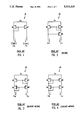
- FIG. 1 illustrates an example of a typical prior art P channel MOS current mirror.
- the function of current mirror 10 is to match channel current I O through transistor M 2 , to channel current I R through transistor M 1 , in order that current I O "mirrors" current I R .
- diode-connected MOS transistor M 1 is in saturation, since V DS1 ⁇ V GS1 .
- V GS2 V GS1 .
- transistor M 2 also operates in saturation with channel current I O through transistor M 2 equal to channel current I R through transistor M 1 . This is true for devices operating both above threshold (V GS ⁇ V T ) and in the subthreshold region (V GS ⁇ V T ). For devices operating above threshold, current I R through transistor M 1 is expressed as: ##EQU1## and current I O is expressed as ##EQU2## where V A is due to channel modulation (Early Voltage).
- transistors M 1 and M 2 have essentially identical process parameters V TH , u o , C ox , etc.
- W 2 channel width of transistor M 2 ;
- L 1 channel length of transistor M 1 ;
- L 2 channel length of transistor M 2 .
- FIG. 2 shows a prior art P channel current mirror commonly known as the "Wilson current mirror.”
- Wilson current mirror 20 provides an increased output resistance as compared with current mirror 10 of FIG. 1.
- the sources of transistors M 1 and M 2 are connected together to positive supply voltage V+, and the gates of transistors M 1 and M 2 are connected together. Therefore, the source-gate voltage of transistors M 1 and M 2 are equal.
- the gate and drain of transistor M 2 are connected together, forcing transistor M 2 into saturation.
- Transistor M 1 therefore mirrors the current flow through transistor M 2 or, since I R is made to flow through transistor M 1 , current I O flowing through the channel of transistor M 2 equals I R .
- Transistor M 4 isolates the drain of transistor M 2 from the voltage applied to the drain of transistor M 4 , thereby preventing any variation in M 4 drain voltage from affecting current I O . Also, transistor M 4 provides negative feedback to current mirror 20, thereby providing a high output resistance.
- FIG. 3 shows a prior art improved Wilson current mirror 30.
- Current mirror 30 operates similarly to current mirror 20 of FIG. 2, and the addition of transistor M 3 matches V DS1 to V DS2 . This provides an improvement as compared with the Wilson current mirror of FIG. 2 in that the Wilson current mirror 20 allows V DS1 to be different than V DS2 , providing another source of error.
- FIG. 4 shows another well known current mirror commonly known as a cascode current mirror.
- Cascode current mirror 40 minimizes variations in I O /I R due to output resistance R O .
- Cascode current mirror 40 is, in effect, a cascade series of 2 current mirror 10 of FIG. 1.
- drain voltage V D1 of transistor M 1 equals drain voltage V D2 of transistor M 2 . If there is a voltage fluctuation increasing the drain voltage of transistor M 4 , drain current I O through transistors M 2 and M 4 remains relatively constant.
- Table 1 shows the minimum saturation voltage (V satmin ) of each of the current mirrors of FIGS. 1-4.
- FIGS. 5-10 depict additional prior art current mirrors which attempt to achieve high output resistances and a relatively low V satmin , although necessarily resulting in a V satmin greater than the V satmin of current mirror 10 of FIG. 1. Furthermore, the prior art current mirrors of FIGS. 5-10 require an additional reference current or are unduly affected by process variations and changes in operating temperature. Therefore, it is desirable to provide a more efficient current source circuit which provides high output impedance, low saturation voltage, and which is unaffected by process variations and changes in temperature.
- An improved current source having high output impedance, low minimum saturation voltage, and less sensitivity to process parameters is achieved by having enhancement mode P channel transistor devices used as current mirror transistors, while a depletion mode P channel transistor is provided as the cascode device.
- a diode connected depletion transistor may be inserted between the gate and drain of the enhancement mode current reference transistor to provide additional reduction in effective saturation voltage as compared with the use of a diode connected enhancement transistor.
- the diode connected depletion device keeps the drains of the enhancement devices at a similar voltage even when the enhancement mode and depletion mode device thresholds, i.e. V T enhancement, does not track V T depletion over temperature or process.
- the current mirror circuit provides not only higher output impedance, lower minimum saturation voltage, but is also less sensitive to process variation.
- FIG. 1 shows an example of a prior art basic current mirror circuit
- FIG. 2 shows an example of a prior art Wilson current mirror circuit in MOS technology
- FIG. 3 shows an example of a prior art improved Wilson current mirror circuit
- FIG. 4 shows an example of a prior art cascode current mirror circuit
- FIGS. 5-10 show other prior art current mirrors
- FIGS. 11-13 show various embodiment of an enhancement-depletion mode cascode current mirror constructed in accordance with the principles of this invention.
- FIG. 14 shows a graphical comparison of the output current to the output voltage of a current mirror constructed in accordance with the principles of this invention
- FIG. 15 is a schematic diagram of a prior art bipolar voltage reference.
- FIG. 16 is a schematic diagram of one embodiment of a bipolar current mirror constructed in accordance with this invention.
- FIG. 11 is a schematic diagram of one embodiment of a current mirror constructed in accordance with the teachings of this invention.
- transistor devices M 3 and M 4 are soft depletion devices, while transistors M 1 and M 2 remain enhancement devices.
- a "soft depletion" device is a P channel device having a threshold voltage on the order of 0 volts or a slightly positive threshold voltage, say for example approximately 0.3 volts.
- V satmin V td +dV dep +dV enh .
- V satmin is within the range of approximately 2 dV, thereby providing a novel current mirror having a high output resistance and a significantly reduced V satmin as compared with the prior art high output resistance current mirrors. Furthermore, being a relatively straightforward circuit, it is not only compact but is also substantially unaffected by variations in process or changes in operating temperature.
- FIG. 12 is a schematic diagram of another embodiment of a current mirror constructed in accordance with the teachings of this invention. Unlike the cascode current mirror described in FIG. 4, in accordance with this embodiment of this invention, transistor devices M 3 and M 4 are soft depletion devices, while transistors M 1 and M 2 remain enhancement devices.
- the minimum saturation voltage V satmin for the embodiment of FIG. 12 is the same as previously described with respect to the embodiment of FIG. 11.
- the embodiment of FIG. 12 provides a novel current mirror having a high output resistance and a significantly reduced V satmin as compared with the prior art high output resistance current mirrors, and which is compact and is substantially unaffected by variations in process or changes in operating temperature.
- FIG. 13 shows an alternative embodiment of an improved current mirror constructed in accordance with the principles of this invention.
- Enhancement-depletion mode cascode current mirror 100 utilizes enhancement mode P channel transistors M 1 and M 2 as the "current mirror” transistors, and depletion mode P channel transistors M 3 and M 4 as the "cascode" transistors. With the gate and drain of depletion mode P channel transistor M 3 connected together, transistor M 3 operates as a diode-connected depletion transistor connected between the gate and drain of current reference transistor M 1 . V T +dV of transistor M 3 is close to zero. With diode-connected depletion M 3 transistor and depletion cascode transistor M 4 , the drains of transistors M 1 and M 2 are maintained at the same voltage. The mirror of FIG.
- transistors M 4 and M 2 have a very small V satmin .
- Transistors M 1 and M 2 are maintained in saturation even when the threshold voltage V te of enhancement mode transistors M 2 and M 1 fail to track V td of depletion mode transistors M 4 and M 3 over temperature and process variations.
- circuit layout is greatly simplified and made more compact by the fact that the gates of transistors M 1 through M 4 are all connected together, as well as minimizing the need to make contacts to source-drain regions.
- FIG. 14 provides a graphical illustration of the high output impedance, achieved by current mirror 100, as compared to the high impedance, higher Vsatmin of a typical prior art current mirror such as current mirror 40 of FIG. 4.
- FIG. 16 is a schematic diagram of one embodiment of a current mirror of this invention fabricated utilizing bipolar transistors, which is an improvement over the prior art voltage reference of FIG. 15.
- Germanium transistors M 3 and M 4 serve the equivalent function of depletion transistors M 3 and M 4 in the MOS embodiment of FIG. 14.
- silicon transistors M 1 and M 2 serve the equivalent purpose of enhancement transistors M 1 and M 2 of the MOS embodiment of FIG. 13.
- the embodiment of FIG. 16 provides a bipolar current mirror having the advantages of high output impedance and low V satmin .
- Table I characterizes various attributes of the prior art current mirrors of FIGS. 1-10 and the embodiments of the novel current mirrors of this invention which are depicted in FIGS. 11-13 and 16.
Landscapes
- Engineering & Computer Science (AREA)
- Microelectronics & Electronic Packaging (AREA)
- Physics & Mathematics (AREA)
- General Physics & Mathematics (AREA)
- Power Engineering (AREA)
- Nonlinear Science (AREA)
- Radar, Positioning & Navigation (AREA)
- Automation & Control Theory (AREA)
- Condensed Matter Physics & Semiconductors (AREA)
- Electromagnetism (AREA)
- Computer Hardware Design (AREA)
- Amplifiers (AREA)
- Control Of Electrical Variables (AREA)
Priority Applications (1)
| Application Number | Priority Date | Filing Date | Title |
|---|---|---|---|
| US08/104,827 US5311115A (en) | 1992-03-18 | 1993-08-11 | Enhancement-depletion mode cascode current mirror |
Applications Claiming Priority (2)
| Application Number | Priority Date | Filing Date | Title |
|---|---|---|---|
| US85352392A | 1992-03-18 | 1992-03-18 | |
| US08/104,827 US5311115A (en) | 1992-03-18 | 1993-08-11 | Enhancement-depletion mode cascode current mirror |
Related Parent Applications (1)
| Application Number | Title | Priority Date | Filing Date |
|---|---|---|---|
| US85352392A Continuation | 1992-03-18 | 1992-03-18 |
Publications (1)
| Publication Number | Publication Date |
|---|---|
| US5311115A true US5311115A (en) | 1994-05-10 |
Family
ID=25316262
Family Applications (1)
| Application Number | Title | Priority Date | Filing Date |
|---|---|---|---|
| US08/104,827 Expired - Lifetime US5311115A (en) | 1992-03-18 | 1993-08-11 | Enhancement-depletion mode cascode current mirror |
Country Status (4)
| Country | Link |
|---|---|
| US (1) | US5311115A (ko) |
| EP (1) | EP0561469A3 (ko) |
| JP (1) | JPH0613820A (ko) |
| KR (1) | KR930020835A (ko) |
Cited By (43)
| Publication number | Priority date | Publication date | Assignee | Title |
|---|---|---|---|---|
| US5373228A (en) * | 1993-02-12 | 1994-12-13 | U.S. Philips Corporation | Integrated circuit having a cascode current mirror |
| US5504444A (en) * | 1994-01-24 | 1996-04-02 | Arithmos, Inc. | Driver circuits with extended voltage range |
| US5515010A (en) * | 1994-09-26 | 1996-05-07 | Texas Instruments Incorporated | Dual voltage level shifted, cascoded current mirror |
| US5625313A (en) * | 1993-09-13 | 1997-04-29 | Nec Corporation | Cascode circuit operable at a low working voltage and having a high output impedance |
| US5640681A (en) * | 1993-11-10 | 1997-06-17 | Motorola, Inc. | Boot-strapped cascode current mirror |
| US5672962A (en) * | 1994-12-05 | 1997-09-30 | Texas Instruments Incorporated | Frequency compensated current output circuit with increased gain |
| US5672960A (en) * | 1994-12-30 | 1997-09-30 | Consorzio Per La Ricerca Sulla Microelettronica Nel Mezzogiorno | Threshold extracting method and circuit using the same |
| US5680038A (en) * | 1996-06-20 | 1997-10-21 | Lsi Logic Corporation | High-swing cascode current mirror |
| US5838192A (en) * | 1996-01-17 | 1998-11-17 | Analog Devices, Inc. | Junction field effect voltage reference |
| US5910738A (en) * | 1995-04-07 | 1999-06-08 | Kabushiki Kaisha Toshiba | Driving circuit for driving a semiconductor device at high speed and method of operating the same |
| US5942912A (en) * | 1996-07-25 | 1999-08-24 | Siemens Aktiengesellschaft | Devices for the self-adjusting setting of the operating point in amplifier circuits with neuron MOS transistors |
| US5966005A (en) * | 1997-12-18 | 1999-10-12 | Asahi Corporation | Low voltage self cascode current mirror |
| US5982206A (en) * | 1996-05-17 | 1999-11-09 | Fujitsu Limited | Transcurrent circuit and current-voltage transforming circuit using the transcurrent circuit |
| US6066944A (en) * | 1999-02-18 | 2000-05-23 | National Semiconductor Corporation | High speed current mirror circuit and method |
| US6133764A (en) * | 1999-01-27 | 2000-10-17 | Motorola, Inc. | Comparator circuit and method |
| US6211659B1 (en) | 2000-03-14 | 2001-04-03 | Intel Corporation | Cascode circuits in dual-Vt, BICMOS and DTMOS technologies |
| WO2002058237A1 (en) * | 2001-01-19 | 2002-07-25 | Koninklijke Philips Electronics N.V. | On-chip cmos oscillator and current reference therefore |
| US20040189362A1 (en) * | 2003-03-28 | 2004-09-30 | Callahan Michael J. | Driver circuit having a slew rate control system with improved linear ramp generator including ground |
| US20050012686A1 (en) * | 2003-03-26 | 2005-01-20 | Mitsuaki Osame | Element substrate and light-emitting device |
| US6963191B1 (en) * | 2003-10-10 | 2005-11-08 | Micrel Inc. | Self-starting reference circuit |
| US20060022746A1 (en) * | 2004-07-29 | 2006-02-02 | Jeong-Min Kim | Output driver for passive matrix organic light emitting diode |
| US7023281B1 (en) | 2004-07-23 | 2006-04-04 | Analog Devices, Inc. | Stably-biased cascode networks |
| US20060164128A1 (en) * | 2005-01-21 | 2006-07-27 | Miller Ira G | Low current power supply monitor circuit |
| US20070085796A1 (en) * | 2003-03-26 | 2007-04-19 | Semiconductor Energy Laboratory Co., Ltd. | Element Substrate and Light Emitting Device |
| US20080030240A1 (en) * | 2006-08-04 | 2008-02-07 | Eric Scheuerlein | Low systematic offset, temperature independent voltage buffering |
| CN100399224C (zh) * | 2005-06-21 | 2008-07-02 | 电子科技大学 | 一种具有极高输出阻抗的电流源 |
| US20080231330A1 (en) * | 2007-03-20 | 2008-09-25 | Masayoshi Takahashi | Ramp generator and circuit pattern inspection apparatus using the same ramp generator |
| US20100207692A1 (en) * | 2007-11-16 | 2010-08-19 | Fujitsu Limited | Bias circuit and control method for bias circuit |
| US20110018520A1 (en) * | 2009-07-24 | 2011-01-27 | Takashi Imura | Reference voltage circuit and electronic device |
| CN101047336B (zh) * | 2006-03-27 | 2012-01-25 | 精工电子有限公司 | 共射共基电路和半导体装置 |
| US20130120050A1 (en) * | 2011-11-10 | 2013-05-16 | Qualcomm Incorporated | Low-power voltage reference circuit |
| US20130193935A1 (en) * | 2012-01-31 | 2013-08-01 | Fsp Technology Inc. | Voltage reference generation circuit using gate-to-source voltage difference and related method thereof, and voltage regulation circuit having common-source configuration and related method thereof |
| US20130328621A1 (en) * | 2012-06-08 | 2013-12-12 | Dong-Kyun Kim | Semiconductor integrated circuit |
| US20140266290A1 (en) * | 2013-03-14 | 2014-09-18 | Bhavin Odedara | Process detection circuit |
| US9383763B1 (en) | 2014-01-03 | 2016-07-05 | Altera Corporation | Multimode current mirror circuitry |
| DE102017202091A1 (de) * | 2016-11-01 | 2018-05-03 | Dialog Semiconductor (Uk) Limited | Hochpräzisions-Spannungsreferenzschaltung |
| US20180167057A1 (en) * | 2016-12-08 | 2018-06-14 | Dong Pan | Apparatus and method for a pvt independent rc delay |
| US20180348807A1 (en) * | 2017-06-01 | 2018-12-06 | Ablic Inc. | Reference voltage circuit and semiconductor device |
| CN110266270A (zh) * | 2018-03-12 | 2019-09-20 | 艾普凌科有限公司 | 振荡电路 |
| US10635126B2 (en) * | 2018-03-28 | 2020-04-28 | Seiko Epson Corporation | Constant current circuit, semiconductor device, electronic apparatus, and method of manufacturing semiconductor device |
| DE10349092B4 (de) | 2003-10-22 | 2020-06-18 | Atmel Corp. | Integrierte Schaltungsanordnung zum Erkennen und Ausgeben von Steuersignalen |
| US11314269B2 (en) * | 2020-01-30 | 2022-04-26 | Morse Micro Pty. Ltd. | Electronic circuit for voltage regulation |
| US11353901B2 (en) | 2019-11-15 | 2022-06-07 | Texas Instruments Incorporated | Voltage threshold gap circuits with temperature trim |
Families Citing this family (14)
| Publication number | Priority date | Publication date | Assignee | Title |
|---|---|---|---|---|
| US5444363A (en) * | 1993-12-16 | 1995-08-22 | Advanced Micro Devices Inc. | Low noise apparatus for receiving an input current and producing an output current which mirrors the input current |
| DE19612269C1 (de) * | 1996-03-28 | 1997-08-28 | Bosch Gmbh Robert | Stromspiegelschaltung |
| JP4118562B2 (ja) | 1999-07-23 | 2008-07-16 | 富士通株式会社 | 低電圧カレントミラー回路 |
| JP2003005710A (ja) * | 2001-06-25 | 2003-01-08 | Nec Corp | 電流駆動回路及び画像表示装置 |
| JP4397697B2 (ja) | 2004-01-15 | 2010-01-13 | 三菱電機株式会社 | 出力回路 |
| DE102004007620B4 (de) | 2004-02-17 | 2008-06-19 | Texas Instruments Deutschland Gmbh | Vorladeschaltkreis für die Inbetriebnahme eines DC-DC-Wandlers zur Spannungserhöhung |
| JP4868868B2 (ja) * | 2006-02-01 | 2012-02-01 | 株式会社リコー | 基準電圧発生回路 |
| JP5388767B2 (ja) * | 2009-09-08 | 2014-01-15 | 新日本無線株式会社 | カレントミラー回路 |
| JP5762755B2 (ja) * | 2010-01-18 | 2015-08-12 | ローム株式会社 | 発光素子の駆動回路およびそれを用いた発光装置 |
| JP2012004627A (ja) * | 2010-06-14 | 2012-01-05 | Toshiba Corp | カレントミラー回路 |
| CN103324229A (zh) * | 2012-03-21 | 2013-09-25 | 广芯电子技术(上海)有限公司 | 恒定电流源 |
| JP2018078349A (ja) * | 2015-03-19 | 2018-05-17 | パナソニックIpマネジメント株式会社 | カレントミラー回路、イメージセンサ、および撮像装置 |
| CN106774593A (zh) * | 2016-12-29 | 2017-05-31 | 北京兆易创新科技股份有限公司 | 一种电流源 |
| JP7177720B2 (ja) * | 2019-02-13 | 2022-11-24 | 日清紡マイクロデバイス株式会社 | 負荷電流検出回路 |
Citations (7)
| Publication number | Priority date | Publication date | Assignee | Title |
|---|---|---|---|---|
| US4241315A (en) * | 1979-02-23 | 1980-12-23 | Harris Corporation | Adjustable current source |
| US4365172A (en) * | 1980-01-11 | 1982-12-21 | Texas Instruments Incorporated | High current static MOS driver circuit with low DC power dissipation |
| EP0183185A2 (en) * | 1984-11-22 | 1986-06-04 | CSELT Centro Studi e Laboratori Telecomunicazioni S.p.A. | Differential reference voltage generator for NMOS single-supply integrated circuits |
| GB2209254A (en) * | 1987-08-29 | 1989-05-04 | Motorola Inc | Current minor amplifier with reduced supply voltage sensitivity |
| US4829231A (en) * | 1987-05-22 | 1989-05-09 | U.S. Philips Corp. | Current mirror having a high output voltage |
| US4855618A (en) * | 1988-02-16 | 1989-08-08 | Analog Devices, Inc. | MOS current mirror with high output impedance and compliance |
| EP0414400A2 (en) * | 1989-08-24 | 1991-02-27 | Delco Electronics Corporation | MOSFET depletion device |
-
1993
- 1993-03-16 EP EP19930200777 patent/EP0561469A3/en not_active Withdrawn
- 1993-03-17 JP JP5057240A patent/JPH0613820A/ja active Pending
- 1993-03-17 KR KR1019930004070A patent/KR930020835A/ko not_active Application Discontinuation
- 1993-08-11 US US08/104,827 patent/US5311115A/en not_active Expired - Lifetime
Patent Citations (8)
| Publication number | Priority date | Publication date | Assignee | Title |
|---|---|---|---|---|
| US4241315A (en) * | 1979-02-23 | 1980-12-23 | Harris Corporation | Adjustable current source |
| US4365172A (en) * | 1980-01-11 | 1982-12-21 | Texas Instruments Incorporated | High current static MOS driver circuit with low DC power dissipation |
| EP0183185A2 (en) * | 1984-11-22 | 1986-06-04 | CSELT Centro Studi e Laboratori Telecomunicazioni S.p.A. | Differential reference voltage generator for NMOS single-supply integrated circuits |
| US4654578A (en) * | 1984-11-22 | 1987-03-31 | Cselt-Centro Studi E Laboratori Telecomunicazioni Spa | Differential reference voltage generator for NMOS single-supply integrated circuits |
| US4829231A (en) * | 1987-05-22 | 1989-05-09 | U.S. Philips Corp. | Current mirror having a high output voltage |
| GB2209254A (en) * | 1987-08-29 | 1989-05-04 | Motorola Inc | Current minor amplifier with reduced supply voltage sensitivity |
| US4855618A (en) * | 1988-02-16 | 1989-08-08 | Analog Devices, Inc. | MOS current mirror with high output impedance and compliance |
| EP0414400A2 (en) * | 1989-08-24 | 1991-02-27 | Delco Electronics Corporation | MOSFET depletion device |
Non-Patent Citations (18)
| Title |
|---|
| Alan B. Grebene, Bipolar and MOS Analog Integrated Circuit Design, John Wiley & Son, 1984, pp. 219 239, 263 303, 709 718. * |
| Alan B. Grebene, Bipolar and MOS Analog Integrated Circuit Design, John Wiley & Son, 1984, pp. 219-239, 263-303, 709-718. |
| G. R. Wilson, A Monolithic Junction FET n p n Operational Amplifier, IEEE Journal of Solid State Circuits, vol. SC 3, No. 4, Dec. 1968, pp. 341 347. * |
| G. R. Wilson, A Monolithic Junction FET-n-p-n Operational Amplifier, IEEE Journal of Solid-State Circuits, vol. SC-3, No. 4, Dec. 1968, pp. 341-347. |
| High Swing MOS Current Mirror with Arbitrarily High Output Resistance P. J. Crawley et al., Electronic Letters, No. 4. * |
| High-Swing MOS Current Mirror with Arbitrarily High Output Resistance P. J. Crawley et al., Electronic Letters, No. 4. |
| O. H. Schade, Jr., "Advances in BiMOS Integrated Circuits", RCA Review, vol. 39, Jun. 1978, pp. 250-277. |
| O. H. Schade, Jr., Advances in BiMOS Integrated Circuits , RCA Review, vol. 39, Jun. 1978, pp. 250 277. * |
| P. R. Gray and R. G. Meyer, MOS Operational Amplifier Design A Tutorial Overview IEEE Journal of Solid State Circuits, vol. SC 17, No. 6, Dec. 1982, pp. 969 982. * |
| P. R. Gray and R. G. Meyer, MOS Operational Amplifier Design-A Tutorial Overview IEEE Journal of Solid-State Circuits, vol. SC-17, No. 6, Dec. 1982, pp. 969-982. |
| P. R. Gray, Basic MOS Operational Amplifier Design An Overview, Analog Mos Integrated Circuits, IEEE Press, N.Y., 1980, pp. 28 49. * |
| P. R. Gray, Basic MOS Operational Amplifier Design-An Overview, Analog Mos Integrated Circuits, IEEE Press, N.Y., 1980, pp. 28-49. |
| R. Gieger, P. Allen and N. Strader, VLSI Design Techniques for Analog and Digital Circuits, McGraw Hill, 1990, p. 352. * |
| R. Gieger, P. Allen and N. Strader, VLSI Design Techniques for Analog and Digital Circuits, McGraw-Hill, 1990, p. 352. |
| R. J. Widlar, Some Circuit Design Techniques for Linear Integrated Circuits, IEEE Transactions on Circuit Theory, vol. CT 12, No. 4, Dec. 1965, pp. 586 590. * |
| R. J. Widlar, Some Circuit Design Techniques for Linear Integrated Circuits, IEEE Transactions on Circuit Theory, vol. CT-12, No. 4, Dec. 1965, pp. 586-590. |
| Y. P. Tsvidis, Design Considerations in Single Channel MOS Analog Integrated Circuits A Tutorial, IEEE Journal of Solid State Circuits, vol. SC 13, No. 3, Jun. 1978, pp. 383 391. * |
| Y. P. Tsvidis, Design Considerations in Single-Channel MOS Analog Integrated Circuits-A Tutorial, IEEE Journal of Solid-State Circuits, vol. SC-13, No. 3, Jun. 1978, pp. 383-391. |
Cited By (71)
| Publication number | Priority date | Publication date | Assignee | Title |
|---|---|---|---|---|
| US5373228A (en) * | 1993-02-12 | 1994-12-13 | U.S. Philips Corporation | Integrated circuit having a cascode current mirror |
| US5625313A (en) * | 1993-09-13 | 1997-04-29 | Nec Corporation | Cascode circuit operable at a low working voltage and having a high output impedance |
| US5640681A (en) * | 1993-11-10 | 1997-06-17 | Motorola, Inc. | Boot-strapped cascode current mirror |
| US5504444A (en) * | 1994-01-24 | 1996-04-02 | Arithmos, Inc. | Driver circuits with extended voltage range |
| US5515010A (en) * | 1994-09-26 | 1996-05-07 | Texas Instruments Incorporated | Dual voltage level shifted, cascoded current mirror |
| US5589800A (en) * | 1994-09-26 | 1996-12-31 | Texas Instruments Incorporated | Dual voltage level shifted, cascoded current mirror |
| US5672962A (en) * | 1994-12-05 | 1997-09-30 | Texas Instruments Incorporated | Frequency compensated current output circuit with increased gain |
| US5672960A (en) * | 1994-12-30 | 1997-09-30 | Consorzio Per La Ricerca Sulla Microelettronica Nel Mezzogiorno | Threshold extracting method and circuit using the same |
| US6111454A (en) * | 1995-04-07 | 2000-08-29 | Kabushiki Kaisha Toshiba | Power supply circuit |
| US5910738A (en) * | 1995-04-07 | 1999-06-08 | Kabushiki Kaisha Toshiba | Driving circuit for driving a semiconductor device at high speed and method of operating the same |
| US5838192A (en) * | 1996-01-17 | 1998-11-17 | Analog Devices, Inc. | Junction field effect voltage reference |
| US5973550A (en) * | 1996-01-17 | 1999-10-26 | Analog Devices, Inc. | Junction field effect voltage reference |
| US5982206A (en) * | 1996-05-17 | 1999-11-09 | Fujitsu Limited | Transcurrent circuit and current-voltage transforming circuit using the transcurrent circuit |
| US5680038A (en) * | 1996-06-20 | 1997-10-21 | Lsi Logic Corporation | High-swing cascode current mirror |
| US5942912A (en) * | 1996-07-25 | 1999-08-24 | Siemens Aktiengesellschaft | Devices for the self-adjusting setting of the operating point in amplifier circuits with neuron MOS transistors |
| US5966005A (en) * | 1997-12-18 | 1999-10-12 | Asahi Corporation | Low voltage self cascode current mirror |
| US6133764A (en) * | 1999-01-27 | 2000-10-17 | Motorola, Inc. | Comparator circuit and method |
| US6066944A (en) * | 1999-02-18 | 2000-05-23 | National Semiconductor Corporation | High speed current mirror circuit and method |
| US6211659B1 (en) | 2000-03-14 | 2001-04-03 | Intel Corporation | Cascode circuits in dual-Vt, BICMOS and DTMOS technologies |
| WO2001069681A2 (en) * | 2000-03-14 | 2001-09-20 | Intel Corporation | Cascode circuits in duel threshold voltage, bicmos and dtmos technologies |
| WO2001069681A3 (en) * | 2000-03-14 | 2002-02-14 | Intel Corp | Cascode circuits in duel threshold voltage, bicmos and dtmos technologies |
| WO2002058237A1 (en) * | 2001-01-19 | 2002-07-25 | Koninklijke Philips Electronics N.V. | On-chip cmos oscillator and current reference therefore |
| US8659523B2 (en) | 2003-03-26 | 2014-02-25 | Semiconductor Energy Laboratory Co., Ltd. | Element substrate and light-emitting device |
| US8759825B2 (en) | 2003-03-26 | 2014-06-24 | Semiconductor Energy Laboratory Co., Ltd. | Element substrate and light emitting device |
| US20050012686A1 (en) * | 2003-03-26 | 2005-01-20 | Mitsuaki Osame | Element substrate and light-emitting device |
| US8400067B2 (en) | 2003-03-26 | 2013-03-19 | Semiconductor Energy Laboratory Co., Ltd. | Element substrate and light emitting device |
| US8212488B2 (en) | 2003-03-26 | 2012-07-03 | Semiconductor Energy Laboratory Co., Ltd. | Element substrate and light emitting device |
| US9147720B2 (en) | 2003-03-26 | 2015-09-29 | Semiconductor Energy Laboratory Co., Ltd. | Element substrate and light emitting device |
| US8026877B2 (en) | 2003-03-26 | 2011-09-27 | Semiconductor Energy Laboratory Co., Ltd. | Element substrate and light-emitting device |
| US8004200B2 (en) | 2003-03-26 | 2011-08-23 | Semiconductor Energy Laboratory Co., Ltd. | Element substrate and light emitting device |
| US9300771B2 (en) | 2003-03-26 | 2016-03-29 | Semiconductor Energy Laboratory Co., Ltd. | Element substrate and light-emitting device |
| US20070085796A1 (en) * | 2003-03-26 | 2007-04-19 | Semiconductor Energy Laboratory Co., Ltd. | Element Substrate and Light Emitting Device |
| US9698207B2 (en) | 2003-03-26 | 2017-07-04 | Semiconductor Energy Laboratory Co., Ltd. | Element substrate and light-emitting device |
| US11430845B2 (en) | 2003-03-26 | 2022-08-30 | Semiconductor Energy Laboratory Co., Ltd. | Element substrate and light-emitting device |
| US20040189362A1 (en) * | 2003-03-28 | 2004-09-30 | Callahan Michael J. | Driver circuit having a slew rate control system with improved linear ramp generator including ground |
| US6927610B2 (en) | 2003-03-28 | 2005-08-09 | Stmicroelectronics, Inc. | Driver circuit having a slew rate control system with improved linear ramp generator including ground |
| US6900672B2 (en) * | 2003-03-28 | 2005-05-31 | Stmicroelectronics, Inc. | Driver circuit having a slew rate control system with improved linear ramp generator including ground |
| US20050007164A1 (en) * | 2003-03-28 | 2005-01-13 | Callahan Michael J. | Driver circuit having a slew rate control system with improved linear ramp generator including ground |
| US6963191B1 (en) * | 2003-10-10 | 2005-11-08 | Micrel Inc. | Self-starting reference circuit |
| DE10349092B4 (de) | 2003-10-22 | 2020-06-18 | Atmel Corp. | Integrierte Schaltungsanordnung zum Erkennen und Ausgeben von Steuersignalen |
| US7023281B1 (en) | 2004-07-23 | 2006-04-04 | Analog Devices, Inc. | Stably-biased cascode networks |
| US20060022746A1 (en) * | 2004-07-29 | 2006-02-02 | Jeong-Min Kim | Output driver for passive matrix organic light emitting diode |
| US20060164128A1 (en) * | 2005-01-21 | 2006-07-27 | Miller Ira G | Low current power supply monitor circuit |
| CN100399224C (zh) * | 2005-06-21 | 2008-07-02 | 电子科技大学 | 一种具有极高输出阻抗的电流源 |
| CN101047336B (zh) * | 2006-03-27 | 2012-01-25 | 精工电子有限公司 | 共射共基电路和半导体装置 |
| CN101894841B (zh) * | 2006-03-27 | 2012-09-05 | 精工电子有限公司 | 共射共基电路和半导体装置 |
| US20080030240A1 (en) * | 2006-08-04 | 2008-02-07 | Eric Scheuerlein | Low systematic offset, temperature independent voltage buffering |
| US20080231330A1 (en) * | 2007-03-20 | 2008-09-25 | Masayoshi Takahashi | Ramp generator and circuit pattern inspection apparatus using the same ramp generator |
| US7816955B2 (en) * | 2007-03-20 | 2010-10-19 | Hitachi, Ltd. | Ramp generator and circuit pattern inspection apparatus using the same ramp generator |
| US7920028B2 (en) | 2007-11-16 | 2011-04-05 | Fujitsu Limited | Bias circuit and control method for bias circuit |
| US20100207692A1 (en) * | 2007-11-16 | 2010-08-19 | Fujitsu Limited | Bias circuit and control method for bias circuit |
| US8212545B2 (en) * | 2009-07-24 | 2012-07-03 | Seiko Instruments Inc. | Reference voltage circuit and electronic device |
| US20110018520A1 (en) * | 2009-07-24 | 2011-01-27 | Takashi Imura | Reference voltage circuit and electronic device |
| US20130120050A1 (en) * | 2011-11-10 | 2013-05-16 | Qualcomm Incorporated | Low-power voltage reference circuit |
| US8786355B2 (en) * | 2011-11-10 | 2014-07-22 | Qualcomm Incorporated | Low-power voltage reference circuit |
| US20130193935A1 (en) * | 2012-01-31 | 2013-08-01 | Fsp Technology Inc. | Voltage reference generation circuit using gate-to-source voltage difference and related method thereof, and voltage regulation circuit having common-source configuration and related method thereof |
| US9218016B2 (en) * | 2012-01-31 | 2015-12-22 | Fsp Technology Inc. | Voltage reference generation circuit using gate-to-source voltage difference and related method thereof |
| US20130328621A1 (en) * | 2012-06-08 | 2013-12-12 | Dong-Kyun Kim | Semiconductor integrated circuit |
| US20140266290A1 (en) * | 2013-03-14 | 2014-09-18 | Bhavin Odedara | Process detection circuit |
| US9383763B1 (en) | 2014-01-03 | 2016-07-05 | Altera Corporation | Multimode current mirror circuitry |
| DE102017202091A1 (de) * | 2016-11-01 | 2018-05-03 | Dialog Semiconductor (Uk) Limited | Hochpräzisions-Spannungsreferenzschaltung |
| US10007289B2 (en) | 2016-11-01 | 2018-06-26 | Dialog Semiconductor (Uk) Limited | High precision voltage reference circuit |
| DE102017202091B4 (de) | 2016-11-01 | 2023-01-26 | Dialog Semiconductor (Uk) Limited | Hochpräzisions-Spannungsreferenzschaltung und Verfahren dafür |
| US10425064B2 (en) * | 2016-12-08 | 2019-09-24 | Micron Technology, Inc. | Apparatus and method for a PVT independent RC delay |
| US20180167057A1 (en) * | 2016-12-08 | 2018-06-14 | Dong Pan | Apparatus and method for a pvt independent rc delay |
| US20180348807A1 (en) * | 2017-06-01 | 2018-12-06 | Ablic Inc. | Reference voltage circuit and semiconductor device |
| US11275399B2 (en) * | 2017-06-01 | 2022-03-15 | Ablic Inc. | Reference voltage circuit including depletion type and enhancement type transistors in a common centroid arrangement |
| CN110266270A (zh) * | 2018-03-12 | 2019-09-20 | 艾普凌科有限公司 | 振荡电路 |
| US10635126B2 (en) * | 2018-03-28 | 2020-04-28 | Seiko Epson Corporation | Constant current circuit, semiconductor device, electronic apparatus, and method of manufacturing semiconductor device |
| US11353901B2 (en) | 2019-11-15 | 2022-06-07 | Texas Instruments Incorporated | Voltage threshold gap circuits with temperature trim |
| US11314269B2 (en) * | 2020-01-30 | 2022-04-26 | Morse Micro Pty. Ltd. | Electronic circuit for voltage regulation |
Also Published As
| Publication number | Publication date |
|---|---|
| KR930020835A (ko) | 1993-10-20 |
| EP0561469A2 (en) | 1993-09-22 |
| JPH0613820A (ja) | 1994-01-21 |
| EP0561469A3 (en) | 1993-10-06 |
Similar Documents
| Publication | Publication Date | Title |
|---|---|---|
| US5311115A (en) | Enhancement-depletion mode cascode current mirror | |
| US4583037A (en) | High swing CMOS cascode current mirror | |
| US7242242B2 (en) | Fast dynamic low-voltage current mirror with compensated error | |
| US4550284A (en) | MOS Cascode current mirror | |
| US5680038A (en) | High-swing cascode current mirror | |
| US5939933A (en) | Intentionally mismatched mirror process inverse current source | |
| US5955874A (en) | Supply voltage-independent reference voltage circuit | |
| EP0140677B1 (en) | Differential amplifier using a constant-current source circuit | |
| JPH03114305A (ja) | 電流ミラー回路 | |
| US4461991A (en) | Current source circuit having reduced error | |
| US6100754A (en) | VT reference voltage for extremely low power supply | |
| US5525927A (en) | MOS current mirror capable of operating in the triode region with minimum output drain-to source voltage | |
| US5672993A (en) | CMOS current mirror | |
| US5793194A (en) | Bias circuit having process variation compensation and power supply variation compensation | |
| US5635869A (en) | Current reference circuit | |
| US4983929A (en) | Cascode current mirror | |
| US5180966A (en) | Current mirror type constant current source circuit having less dependence upon supplied voltage | |
| US5801523A (en) | Circuit and method of providing a constant current | |
| US5936433A (en) | Comparator including a transconducting inverter biased to operate in subthreshold | |
| US20040056708A1 (en) | Fast dynamic low-voltage current mirror with compensated error | |
| US4602207A (en) | Temperature and power supply stable current source | |
| US5610505A (en) | Voltage-to-current converter with MOS reference resistor | |
| US6392465B1 (en) | Sub-threshold CMOS integrator | |
| KR930001294B1 (ko) | 전류미러(current mirror) | |
| US5864228A (en) | Current mirror current source with current shunting circuit |
Legal Events
| Date | Code | Title | Description |
|---|---|---|---|
| STCF | Information on status: patent grant |
Free format text: PATENTED CASE |
|
| FPAY | Fee payment |
Year of fee payment: 4 |
|
| FPAY | Fee payment |
Year of fee payment: 8 |
|
| REMI | Maintenance fee reminder mailed | ||
| FEPP | Fee payment procedure |
Free format text: PAYOR NUMBER ASSIGNED (ORIGINAL EVENT CODE: ASPN); ENTITY STATUS OF PATENT OWNER: LARGE ENTITY |
|
| FPAY | Fee payment |
Year of fee payment: 12 |