US5083295A - Integrated memory circuit with interconnected sense amplifiers - Google Patents
Integrated memory circuit with interconnected sense amplifiers Download PDFInfo
- Publication number
- US5083295A US5083295A US07/444,929 US44492989A US5083295A US 5083295 A US5083295 A US 5083295A US 44492989 A US44492989 A US 44492989A US 5083295 A US5083295 A US 5083295A
- Authority
- US
- United States
- Prior art keywords
- memory
- transistor
- transistors
- sense amplifiers
- integrated circuit
- Prior art date
- Legal status (The legal status is an assumption and is not a legal conclusion. Google has not performed a legal analysis and makes no representation as to the accuracy of the status listed.)
- Expired - Lifetime
Links
Images

Classifications
-
- G—PHYSICS
- G11—INFORMATION STORAGE
- G11C—STATIC STORES
- G11C11/00—Digital stores characterised by the use of particular electric or magnetic storage elements; Storage elements therefor
- G11C11/21—Digital stores characterised by the use of particular electric or magnetic storage elements; Storage elements therefor using electric elements
- G11C11/34—Digital stores characterised by the use of particular electric or magnetic storage elements; Storage elements therefor using electric elements using semiconductor devices
-
- G—PHYSICS
- G11—INFORMATION STORAGE
- G11C—STATIC STORES
- G11C7/00—Arrangements for writing information into, or reading information out from, a digital store
- G11C7/06—Sense amplifiers; Associated circuits, e.g. timing or triggering circuits
- G11C7/065—Differential amplifiers of latching type
-
- G—PHYSICS
- G11—INFORMATION STORAGE
- G11C—STATIC STORES
- G11C11/00—Digital stores characterised by the use of particular electric or magnetic storage elements; Storage elements therefor
- G11C11/21—Digital stores characterised by the use of particular electric or magnetic storage elements; Storage elements therefor using electric elements
- G11C11/34—Digital stores characterised by the use of particular electric or magnetic storage elements; Storage elements therefor using electric elements using semiconductor devices
- G11C11/40—Digital stores characterised by the use of particular electric or magnetic storage elements; Storage elements therefor using electric elements using semiconductor devices using transistors
- G11C11/41—Digital stores characterised by the use of particular electric or magnetic storage elements; Storage elements therefor using electric elements using semiconductor devices using transistors forming static cells with positive feedback, i.e. cells not needing refreshing or charge regeneration, e.g. bistable multivibrator or Schmitt trigger
- G11C11/413—Auxiliary circuits, e.g. for addressing, decoding, driving, writing, sensing, timing or power reduction
- G11C11/414—Auxiliary circuits, e.g. for addressing, decoding, driving, writing, sensing, timing or power reduction for memory cells of the bipolar type
- G11C11/416—Read-write [R-W] circuits
-
- G—PHYSICS
- G11—INFORMATION STORAGE
- G11C—STATIC STORES
- G11C11/00—Digital stores characterised by the use of particular electric or magnetic storage elements; Storage elements therefor
- G11C11/21—Digital stores characterised by the use of particular electric or magnetic storage elements; Storage elements therefor using electric elements
- G11C11/34—Digital stores characterised by the use of particular electric or magnetic storage elements; Storage elements therefor using electric elements using semiconductor devices
- G11C11/40—Digital stores characterised by the use of particular electric or magnetic storage elements; Storage elements therefor using electric elements using semiconductor devices using transistors
- G11C11/41—Digital stores characterised by the use of particular electric or magnetic storage elements; Storage elements therefor using electric elements using semiconductor devices using transistors forming static cells with positive feedback, i.e. cells not needing refreshing or charge regeneration, e.g. bistable multivibrator or Schmitt trigger
- G11C11/413—Auxiliary circuits, e.g. for addressing, decoding, driving, writing, sensing, timing or power reduction
- G11C11/417—Auxiliary circuits, e.g. for addressing, decoding, driving, writing, sensing, timing or power reduction for memory cells of the field-effect type
- G11C11/419—Read-write [R-W] circuits
Definitions
- the invention relates to an integrated circuit with a memory, comprising a matrix of memory cells and sense amplifiers which are coupled thereto and outputs of which are connected to one another and to a common data bus.
- a circuit of the kind set forth is known from IEEE Transactions on Electron Devices, Vol. ED-31, No. 9, September 1984: Masayuki et al., "Design of GaAs 1 kBit Static Ram", notably from FIG. 1.
- the switching speed of the sense amplifiers used in the circuit is inter alia dependent on the parasitic capacitive load formed by the common read lines (read bus). This capacitive load is generally proportional to the length of these lines and hence dependent on the number of memory columns to be coupled.
- the access time for reading a memory cell will be dependent on the number of columns or the dimensions of the transistors in the sense amplifiers must be adapted in view of the above capacitive load when the desired number of parallel memory columns is changed, so that a new design is required for a part of the memory circuit.
- the repeated redimensioning of transistors requires additional design time and hence has a cost-increasing effect.
- an integrated circuit with a memory in accordance with the invention is characterized in that there are provided activatable and deactivatable coupling means for coupling a single memory column to the input of each sense amplifier, there also being provided activation means for simultaneously activating each sense amplifier.
- An integrated circuit with a memory in accordance with the invention offers the advantage that the access time for reading a memory cell remains the same for an arbitrary number of memory columns, and that the transistors in the sense amplifiers need be dimensioned only once, resulting in a saving as regards time and costs.
- the access time remains the same because, even though the capacitive load of the read lines increases when the number of memory columns to be connected to common read lines is increased, the number of parallel operating sense amplifiers connected to the read lines is also increased. Because of the sense amplifier (amplifiers) in the additional memory column (columns), the ratio of total gain to capacitive load remains substantially constant.
- the inputs of the sense amplifiers are interconnected via common input lines, so that when information is read from a memory cell in a given column, the other sense amplifiers are simultaneously activated with the same information.
- the common input lines also form a capacitive load for the memory cell to be read, which parasitic capacitance is proportional to the number of memory columns.
- the parasitic bit line capacitance will be many times higher than the parasitic capacitance of said connection, because the number of rows in a memory column usually exceeds the number of parallel-connected memory columns (for example, 64 rows and 4 columns).
- the total parasitic capacitive load for a selected memory cell is substantially constant and substantially equal to the parasitic bit line capacitance.
- a preferred embodiment of an integrated circuit with a memory in accordance with the invention is characterized in that the input of each sense amplifier is connected to its output. This offers the advantage that the connection between the sense amplifier inputs is already formed by the read lines present. As a result, the chip surface area required for the memory circuit is smaller and the chip lay-out is simpler. Moreover, the memory information is taken over more quickly because of the effect of the sense amplifiers on the information signal.
- Another embodiment of an integrated circuit with a memory in accordance with the invention is characterized in that a sense amplifier is provided for each memory column. This offers the advantage that the memory circuit in accordance with the invention can be extended by way of single columns.
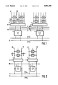
- FIG. 1 shows a memory circuit in accordance with the invention
- FIG. 2 shows a preferred embodiment of a memory circuit in accordance with the invention.
- FIG. 3 is a detailed representation of a preferred embodiment of a part of the memory circuit shown in FIG. 2.
- FIG. 1 shows a memory circuit in accordance with the invention.
- the memory circuit comprises memory cells M which are arranged in rows and columns. Via bit lines BI and BI and a column decoder 3, the memory cells M are connected to the respective inputs of a sense amplifier 4 and to common input lines 1 and 2. The respective outputs of the sense amplifiers 4 are connected to common read lines D and D, respectively. The sense amplifiers are connected to a common input line BS.
- the operation of the part of the memory circuit which is shown in FIG. 1 will be described as regards the reading of information from a memory cell M.
- a row selection signal (not shown)
- a row of memory cells M is selected.
- the memory information of the relevant row of memory cells M is applied to the relevant bit lines BI and BI.
- a decoding signal A and the column decoder 3 a single memory column is selected.
- Memory information of a single memory cell M is thus applied to the input lines 1 and 2.
- the sense amplifiers 4 are simultaneously activated by means of a control signal on the common input line BS, so that the memory information is applied to the read lines D and D in amplified form.
- the bit lines BI and BI and the input lines 1 and 2 will have a parasitic capacitance C b and C 1 , respectively, with respect to the substate which is usually connected to a power supply terminal.
- the value of said parasitic capacitances C b and C 1 is directly proportional to the length of the bit lines BI and BI and the input lines 1 and 2, respectively. Because the length of the input lines 1 and 2 is proportional to the selected number of memory columns in a matrix of the memory circuit, the value of the parasitic capacitance C 1 is proportional to the number of memory columns selected.
- a selected memory cell is loaded by the sum of the bit line capacitance C b and the input line capacitance C 1 .
- the bit line capacitance C b will be many times higher than the input line capacitance C 1 (C b >>C 1 ), because the length of a memory column is usually selected to be greater than the number of memory columns to be connected to the common input lines 1 and 2.
- the sum of the above capacitances then approximately equals the bit line capacitance C b and remains approximately constant when the number of memory columns to be connected to the common input lines 1 and 2 is selected to be larger or smaller.
- the outputs of the sense amplifiers 4 are loaded by the parasitic capacitance C d of the read lines D and D.
- the value of the capacitance C d is directly proportional to the length of the read line D or D, which length is also proportional to the number of memory columns connected to the common input lines 1 and 2.
- the speed at which the read line capacitance C d can be charged or discharged depends on the value of the capacitance C d , but in the memory circuit in accordance with the invention it also depends on the number of sense amplifiers 4 connected to the common read lines D and D. This is because, when the number of sense amplifiers 4 increases, the total gain power of the sense amplifiers 4 increases because the sense amplifiers 4 are simultaneously activated by a signal on the common input line BS.
- FIG. 2 shows a preferred embodiment of a memory circuit in accordance with the invention. Elements which correspond to elements shown in FIG. 1 are denoted by corresponding reference symbols.
- the sense amplifiers comprise combined inputs and outputs so that the common input lines 1 and 2 of FIG. 1 can be dispensed with. Moreover, in this case each memory column is connected to a separate sense amplifier 4.
- the operation of the part of the memory circuit shown in FIG. 2 corresponds substantially to that of the circuit shown in FIG. 1.
- the relevant cell information is applied to the relevant bit lines BI and BI.
- a decoder signal A and the column decoder 3 a single memory column is selected. This information is then present on the input/output of the sense amplifier 4 in the relevant column. Via the common read lines D and D this information is also available on the input/output of every other sense amplifier 4 connected thereto.
- the cell information is applied to the common read lines D and D in amplified form.
- the read line capacitance C d again increases when the number of memory columns increases, but the total gain of the sense amplifiers 4 then also increases, so that the speed of reading again remains substantially constant.
- the selection of sense amplifiers 4 having combined inputs and outputs in FIG. 2 offers the advantage that the input lines 1 and 2 shown in FIG. 1 can be dispensed with. As a result, less chip surface area will be required. Moreover, the memory information is taken over more quickly by the sense amplifiers, because the sense amplifiers amplify the information signal (latch).
- the selection of a sense amplifier 4 provided for each memory column offers the advantage that the memory circuit can be extended with single columns. In an embodiment of a memory circuit in accordance with the invention as shown in FIG. 1, the memory circuit can be extended only in multiples of two columns because of the presence of a single sense amplifier.
- FIG. 3 is a detailed representation of a preferred embodiment of a sense amplifier 4 and a column decoder 3 as shown in FIG. 2.
- the single sense amplifier shown comprises three NMOS transistors T1, T2 and T7 and six PMOS transistors T3, T4, T5, T6, T8 and T9.
- the sources of the transistors T1 and T2 are connected to one another and to the drain of the transistor T7.
- the drains of the transistors T1 and T5 are connected to one another, to the gates of the transistors T2 and T6, and to the drain of the transistor T3.
- the drains of the transistors T2 and T6 are connected to one another, to the gates of the transistors T1 and T5, and to the drain of the transistor T4.
- the gates of the transistors T3 and T4 are connected to an input terminal YR (for the reception of a decoder signal A), the sources of the transistors T3 and T4 being connected to a bit line BI, BI, respectively.
- the drains of the transistors T3 and T8 and the drains of the transistors T4 and T9 are connected to a read line D, D, respectively.
- the sources of the transistors T5, T6, T7 and T9, and the source of the transistor T7 are coupled to the power supply terminal U1, U2, respectively.
- the gates of the transistors T8 and T9 are connected to an input line BS.
- the gate of the transistor T7 is connected to an input line BS'.
- n-type transistors are to be understood to mean either n-channel field-effect transistors or bipolar npn-transistors
- p-type transistors are to be understood to mean either p-channel field-effect transistors or bipolar pnp-transistors.
- the circuit shown in FIG. 3 operates as follows. In the case of a "low" signal of the input lines BS and BS', the transistors T8 and T9 are turned on and the transistor T7 is turned off. The read lines D and D are thus precharged via the transistors T8 and T9. In response to a subsequent "high" signal on the input line BS, the transistors T8 and T9 are turned off. In the case of a "low” signal A on the input line YR, which signal originates, for example from an address decoder circuit (not shown) which is included in an integrated memory circuit for the selection of a column of the memory circuit, the transistors T3 and T4 are turned on.
- the read line D remains “high” and the non-read line D is partly discharged by a non-bit line BI.
- the transistor T7 is turned on. Because of the "high” state of the node 10, the transistor T2 is turned on so that the node 20 is fully discharged and subsequently remains “low”. As a result, the transistor T5 is turned on so that the node 10 remains "high”.
- the non-read line D remains “high” and the read line D is partly discharged by the bit line BI.
- the transistor T7 is turned on. Because of the "high” state of the node 20, the transistor T1 is turned on so that the node 10 is fully discharged and subsequently remains “low”. As a result, the transistor T6 is turned on and the node 20 remains "high”.
- the signal on the input line BS' can be simply derived from the signal on the input line BS by means of delay elements (for example, by means of two series-connected inverters (not shown).
- the nodes 10 and 20 are connected to a common read line D and a non-read line D', respectively, in the described manner.
- these read lines have a parasitic capacitance which is proportional to the number of memory columns connected to the read lines D and D.
- the speed at which said capacitance can be discharged during successive read operations depends on the parasitic capacitance of the read lines D and D and on the conductivity of the transistors T1, T2 and T7, but in the memory circuit in accordance with the invention it is also dependent on the number of sense amplifiers connected to the common read lines D and D.
- the latter can be illustrated as follows: a voltage at the node 10 or the node 20 of the sense amplifier shown in FIG.
- the sense amplifier shown in FIG. 3 is constructed by means of MOS-transistors; however, said NMOS-transistors and PMOS-transistors can be replaced by bipolar npn-transistors and pnp-transistors, respectively.
Landscapes
- Engineering & Computer Science (AREA)
- Computer Hardware Design (AREA)
- Microelectronics & Electronic Packaging (AREA)
- Static Random-Access Memory (AREA)
- Dram (AREA)
Applications Claiming Priority (2)
| Application Number | Priority Date | Filing Date | Title |
|---|---|---|---|
| NL8802973 | 1988-12-02 | ||
| NL8802973A NL8802973A (nl) | 1988-12-02 | 1988-12-02 | Geintegreerde geheugenschakeling. |
Publications (1)
| Publication Number | Publication Date |
|---|---|
| US5083295A true US5083295A (en) | 1992-01-21 |
Family
ID=19853327
Family Applications (1)
| Application Number | Title | Priority Date | Filing Date |
|---|---|---|---|
| US07/444,929 Expired - Lifetime US5083295A (en) | 1988-12-02 | 1989-11-30 | Integrated memory circuit with interconnected sense amplifiers |
Country Status (8)
| Country | Link |
|---|---|
| US (1) | US5083295A (fi) |
| EP (1) | EP0374995B1 (fi) |
| JP (1) | JP2755450B2 (fi) |
| KR (1) | KR900010776A (fi) |
| DE (1) | DE68918568T2 (fi) |
| FI (1) | FI895717A0 (fi) |
| IE (1) | IE64653B1 (fi) |
| NL (1) | NL8802973A (fi) |
Cited By (11)
| Publication number | Priority date | Publication date | Assignee | Title |
|---|---|---|---|---|
| US5323349A (en) * | 1991-10-31 | 1994-06-21 | Mitsubishi Denki Kabushiki Kaisha | Dynamic semiconductor memory device having separate read and write data bases |
| US5430677A (en) * | 1991-02-11 | 1995-07-04 | Intel Corporation | Architecture for reading information from a memory array |
| US5467312A (en) * | 1993-04-21 | 1995-11-14 | Plessey Semiconductors Limited | Random access memory |
| US5477489A (en) * | 1995-03-20 | 1995-12-19 | Exponential Technology, Inc. | High-stability CMOS multi-port register file memory cell with column isolation and current-mirror row line driver |
| US5506524A (en) * | 1995-03-01 | 1996-04-09 | Lin; Jyhfong | Low-voltage low-power dynamic folded sense amplifier |
| US5508644A (en) * | 1994-09-28 | 1996-04-16 | Motorola, Inc. | Sense amplifier for differential voltage detection with low input capacitance |
| US5646883A (en) * | 1992-12-22 | 1997-07-08 | Siemens Aktiengesellschaft | Signal sensing circuits for memory system using dynamic gain memory |
| US5878269A (en) * | 1992-03-27 | 1999-03-02 | National Semiconductor Corporation | High speed processor for operation at reduced operating voltage |
| US6208574B1 (en) | 1992-11-12 | 2001-03-27 | United Memories, Inc. | Sense amplifier with local column read amplifier and local data write drivers |
| US6268747B1 (en) * | 1999-01-27 | 2001-07-31 | Stmicroelectronics Limited | Dynamic voltage sense amplifier |
| US20080123455A1 (en) * | 2006-11-24 | 2008-05-29 | Hynix Semiconductor Inc. | Sense amplifier of semiconductor memory device |
Citations (7)
| Publication number | Priority date | Publication date | Assignee | Title |
|---|---|---|---|---|
| US3879621A (en) * | 1973-04-18 | 1975-04-22 | Ibm | Sense amplifier |
| US4131951A (en) * | 1976-05-17 | 1978-12-26 | Tokyo Shibaura Electric Co., Ltd. | High speed complementary MOS memory |
| JPS5694574A (en) * | 1979-12-27 | 1981-07-31 | Toshiba Corp | Complementary mos sense circuit |
| US4555777A (en) * | 1984-08-14 | 1985-11-26 | Texas Instruments Incorporated | Sense amplifier circuit for dynamic read/write memory |
| US4804871A (en) * | 1987-07-28 | 1989-02-14 | Advanced Micro Devices, Inc. | Bit-line isolated, CMOS sense amplifier |
| US4813021A (en) * | 1981-07-27 | 1989-03-14 | Tokyo Shibayra Denki Kabushiki Kaisha | Semiconductor memory device with delayed precharge signals |
| US4879692A (en) * | 1987-06-04 | 1989-11-07 | Nec Corporation | Dynamic memory circuit with improved sensing scheme |
-
1988
- 1988-12-02 NL NL8802973A patent/NL8802973A/nl not_active Application Discontinuation
-
1989
- 1989-11-27 EP EP89203007A patent/EP0374995B1/en not_active Expired - Lifetime
- 1989-11-27 DE DE68918568T patent/DE68918568T2/de not_active Expired - Lifetime
- 1989-11-29 JP JP1307822A patent/JP2755450B2/ja not_active Expired - Lifetime
- 1989-11-29 KR KR1019890017375A patent/KR900010776A/ko active IP Right Grant
- 1989-11-29 FI FI895717A patent/FI895717A0/fi not_active Application Discontinuation
- 1989-11-30 US US07/444,929 patent/US5083295A/en not_active Expired - Lifetime
- 1989-11-30 IE IE383389A patent/IE64653B1/en not_active IP Right Cessation
Patent Citations (7)
| Publication number | Priority date | Publication date | Assignee | Title |
|---|---|---|---|---|
| US3879621A (en) * | 1973-04-18 | 1975-04-22 | Ibm | Sense amplifier |
| US4131951A (en) * | 1976-05-17 | 1978-12-26 | Tokyo Shibaura Electric Co., Ltd. | High speed complementary MOS memory |
| JPS5694574A (en) * | 1979-12-27 | 1981-07-31 | Toshiba Corp | Complementary mos sense circuit |
| US4813021A (en) * | 1981-07-27 | 1989-03-14 | Tokyo Shibayra Denki Kabushiki Kaisha | Semiconductor memory device with delayed precharge signals |
| US4555777A (en) * | 1984-08-14 | 1985-11-26 | Texas Instruments Incorporated | Sense amplifier circuit for dynamic read/write memory |
| US4879692A (en) * | 1987-06-04 | 1989-11-07 | Nec Corporation | Dynamic memory circuit with improved sensing scheme |
| US4804871A (en) * | 1987-07-28 | 1989-02-14 | Advanced Micro Devices, Inc. | Bit-line isolated, CMOS sense amplifier |
Non-Patent Citations (6)
| Title |
|---|
| IBM TDB vol. 18, No. 6, Nov. 1975: Read and Write For Random Access Memory Array pp. 1849 1850. * |
| IBM TDB vol. 28, No. 3, Aug. 1985: Bitline Restore Circuit for High Speed CMOS Arrays pp. 1227 1228. * |
| IBM TDB vol. 29, No. 5, Oct. 1986 Dense Sense Amplifier/Latch Combination pp. 2160 2161. * |
| IBM-TDB vol. 18, No. 6, Nov. 1975: "Read and Write For Random Access Memory Array" pp. 1849-1850. |
| IBM-TDB vol. 28, No. 3, Aug. 1985: "Bitline Restore Circuit for High Speed CMOS Arrays" pp. 1227-1228. |
| IBM-TDB vol. 29, No. 5, Oct. 1986 "Dense Sense Amplifier/Latch Combination" pp. 2160-2161. |
Cited By (14)
| Publication number | Priority date | Publication date | Assignee | Title |
|---|---|---|---|---|
| US5430677A (en) * | 1991-02-11 | 1995-07-04 | Intel Corporation | Architecture for reading information from a memory array |
| US5323349A (en) * | 1991-10-31 | 1994-06-21 | Mitsubishi Denki Kabushiki Kaisha | Dynamic semiconductor memory device having separate read and write data bases |
| US5878269A (en) * | 1992-03-27 | 1999-03-02 | National Semiconductor Corporation | High speed processor for operation at reduced operating voltage |
| US6275432B1 (en) | 1992-11-12 | 2001-08-14 | United Memories, Inc. | Method of reading and writing data using local data read and local data write circuits |
| US6249469B1 (en) * | 1992-11-12 | 2001-06-19 | United Memories, Inc. | Sense amplifier with local sense drivers and local read amplifiers |
| US6208574B1 (en) | 1992-11-12 | 2001-03-27 | United Memories, Inc. | Sense amplifier with local column read amplifier and local data write drivers |
| US5646883A (en) * | 1992-12-22 | 1997-07-08 | Siemens Aktiengesellschaft | Signal sensing circuits for memory system using dynamic gain memory |
| US5467312A (en) * | 1993-04-21 | 1995-11-14 | Plessey Semiconductors Limited | Random access memory |
| US5508644A (en) * | 1994-09-28 | 1996-04-16 | Motorola, Inc. | Sense amplifier for differential voltage detection with low input capacitance |
| US5506524A (en) * | 1995-03-01 | 1996-04-09 | Lin; Jyhfong | Low-voltage low-power dynamic folded sense amplifier |
| US5477489A (en) * | 1995-03-20 | 1995-12-19 | Exponential Technology, Inc. | High-stability CMOS multi-port register file memory cell with column isolation and current-mirror row line driver |
| US6268747B1 (en) * | 1999-01-27 | 2001-07-31 | Stmicroelectronics Limited | Dynamic voltage sense amplifier |
| US20080123455A1 (en) * | 2006-11-24 | 2008-05-29 | Hynix Semiconductor Inc. | Sense amplifier of semiconductor memory device |
| US7525859B2 (en) * | 2006-11-24 | 2009-04-28 | Hynix Semiconductor Inc. | Sense amplifier of semiconductor memory device |
Also Published As
| Publication number | Publication date |
|---|---|
| IE893833L (en) | 1990-06-02 |
| DE68918568T2 (de) | 1995-04-27 |
| NL8802973A (nl) | 1990-07-02 |
| EP0374995B1 (en) | 1994-09-28 |
| EP0374995A1 (en) | 1990-06-27 |
| FI895717A0 (fi) | 1989-11-29 |
| JPH02189789A (ja) | 1990-07-25 |
| JP2755450B2 (ja) | 1998-05-20 |
| DE68918568D1 (de) | 1994-11-03 |
| KR900010776A (ko) | 1990-07-09 |
| IE64653B1 (en) | 1995-08-23 |
Similar Documents
| Publication | Publication Date | Title |
|---|---|---|
| US5023841A (en) | Double stage sense amplifier for random access memories | |
| KR930000712B1 (ko) | 반도체 집적회로 | |
| US5226014A (en) | Low power pseudo-static ROM | |
| US5083295A (en) | Integrated memory circuit with interconnected sense amplifiers | |
| US5068830A (en) | High speed static ram sensing system | |
| US7221581B2 (en) | Memory with storage cells biased in groups | |
| US5373473A (en) | Amplifier circuit and semiconductor memory device employing the same | |
| US5387827A (en) | Semiconductor integrated circuit having logic gates | |
| US5880990A (en) | Dual port memory apparatus operating a low voltage to maintain low operating current during charging and discharging | |
| US4860257A (en) | Level shifter for an input/output bus in a CMOS dynamic ram | |
| US5253137A (en) | Integrated circuit having a sense amplifier | |
| JP2760634B2 (ja) | 集積メモリ | |
| EP0503524B1 (en) | Semiconductor memory device | |
| US6879524B2 (en) | Memory I/O buffer using shared read/write circuitry | |
| US5172340A (en) | Double stage bipolar sense amplifier for BICMOS SRAMS with a common base amplifier in the final stage | |
| EP0316877B1 (en) | Semiconductor memory device with improved output circuit | |
| US4604534A (en) | Highly sensitive high performance sense amplifiers | |
| JP2752197B2 (ja) | ディジタル・メモリ・システム | |
| US5982692A (en) | Bit line boost amplifier | |
| KR100227300B1 (ko) | 반도체 기억 장치 | |
| US4037217A (en) | Read-only memory using complementary conductivity type insulated gate field effect transistors | |
| KR100190366B1 (ko) | 반도체 메모리 장치 및 그 전원인가방법 | |
| US5065367A (en) | High-gain sense amplifiers array for high-speed read operation | |
| US4780853A (en) | Memory device | |
| US5943274A (en) | Method and apparatus for amplifying a signal to produce a latched digital signal |
Legal Events
| Date | Code | Title | Description |
|---|---|---|---|
| AS | Assignment |
Owner name: U.S. PHILIPS CORPORATION, 100 E. 42ND ST., NEW YOR Free format text: ASSIGNMENT OF ASSIGNORS INTEREST.;ASSIGNORS:LAMMERTS, JUDOCUS A.M.;RITZERFELD, WILLEM G.J.;TOOHER, MICHAEL J.;REEL/FRAME:005188/0138;SIGNING DATES FROM 19891025 TO 19891027 |
|
| STCF | Information on status: patent grant |
Free format text: PATENTED CASE |
|
| FPAY | Fee payment |
Year of fee payment: 4 |
|
| FPAY | Fee payment |
Year of fee payment: 8 |
|
| FPAY | Fee payment |
Year of fee payment: 12 |
|
| AS | Assignment |
Owner name: NXP B.V., NETHERLANDS Free format text: ASSIGNMENT OF ASSIGNORS INTEREST;ASSIGNOR:U.S. PHILIPS CORPORATION;REEL/FRAME:018635/0755 Effective date: 20061127 |
|
| AS | Assignment |
Owner name: MORGAN STANLEY SENIOR FUNDING, INC., ENGLAND Free format text: SECURITY AGREEMENT;ASSIGNOR:NXP B.V.;REEL/FRAME:018806/0201 Effective date: 20061201 |
|
| AS | Assignment |
Owner name: NXP B.V., NETHERLANDS Free format text: RELEASE BY SECURED PARTY;ASSIGNOR:MORGAN STANLEY SENIOR FUNDING, INC;REEL/FRAME:050315/0443 Effective date: 20190903 |