US4047220A - Bipolar transistor structure having low saturation resistance - Google Patents
Bipolar transistor structure having low saturation resistance Download PDFInfo
- Publication number
- US4047220A US4047220A US05/644,338 US64433875A US4047220A US 4047220 A US4047220 A US 4047220A US 64433875 A US64433875 A US 64433875A US 4047220 A US4047220 A US 4047220A
- Authority
- US
- United States
- Prior art keywords
- region
- collector
- conductivity type
- regions
- resistance
- Prior art date
- Legal status (The legal status is an assumption and is not a legal conclusion. Google has not performed a legal analysis and makes no representation as to the accuracy of the status listed.)
- Expired - Lifetime
Links
- 239000004065 semiconductor Substances 0.000 claims description 26
- 239000000758 substrate Substances 0.000 claims description 17
- 230000007480 spreading Effects 0.000 claims description 6
- 239000004020 conductor Substances 0.000 claims description 2
- 238000009792 diffusion process Methods 0.000 description 15
- 230000015556 catabolic process Effects 0.000 description 7
- 238000004519 manufacturing process Methods 0.000 description 5
- 238000004804 winding Methods 0.000 description 5
- 238000000034 method Methods 0.000 description 3
- VYPSYNLAJGMNEJ-UHFFFAOYSA-N Silicium dioxide Chemical compound O=[Si]=O VYPSYNLAJGMNEJ-UHFFFAOYSA-N 0.000 description 2
- 230000008901 benefit Effects 0.000 description 2
- 239000002775 capsule Substances 0.000 description 2
- 230000006872 improvement Effects 0.000 description 2
- 238000002955 isolation Methods 0.000 description 2
- 239000000463 material Substances 0.000 description 2
- 230000004048 modification Effects 0.000 description 2
- 238000012986 modification Methods 0.000 description 2
- ZOKXTWBITQBERF-UHFFFAOYSA-N Molybdenum Chemical compound [Mo] ZOKXTWBITQBERF-UHFFFAOYSA-N 0.000 description 1
- XAGFODPZIPBFFR-UHFFFAOYSA-N aluminium Chemical compound [Al] XAGFODPZIPBFFR-UHFFFAOYSA-N 0.000 description 1
- 229910052782 aluminium Inorganic materials 0.000 description 1
- 230000003466 anti-cipated effect Effects 0.000 description 1
- 238000010420 art technique Methods 0.000 description 1
- 238000006243 chemical reaction Methods 0.000 description 1
- 230000001419 dependent effect Effects 0.000 description 1
- 238000010586 diagram Methods 0.000 description 1
- 239000007772 electrode material Substances 0.000 description 1
- 239000011810 insulating material Substances 0.000 description 1
- 229910052750 molybdenum Inorganic materials 0.000 description 1
- 239000011733 molybdenum Substances 0.000 description 1
- 229910021420 polycrystalline silicon Inorganic materials 0.000 description 1
- 230000008569 process Effects 0.000 description 1
- 230000009467 reduction Effects 0.000 description 1
- 235000012239 silicon dioxide Nutrition 0.000 description 1
- 239000000377 silicon dioxide Substances 0.000 description 1
Images
Classifications
-
- H—ELECTRICITY
- H10—SEMICONDUCTOR DEVICES; ELECTRIC SOLID-STATE DEVICES NOT OTHERWISE PROVIDED FOR
- H10D—INORGANIC ELECTRIC SEMICONDUCTOR DEVICES
- H10D84/00—Integrated devices formed in or on semiconductor substrates that comprise only semiconducting layers, e.g. on Si wafers or on GaAs-on-Si wafers
- H10D84/60—Integrated devices formed in or on semiconductor substrates that comprise only semiconducting layers, e.g. on Si wafers or on GaAs-on-Si wafers characterised by the integration of at least one component covered by groups H10D10/00 or H10D18/00, e.g. integration of BJTs
- H10D84/641—Combinations of only vertical BJTs
- H10D84/642—Combinations of non-inverted vertical BJTs of the same conductivity type having different characteristics, e.g. Darlington transistors
Definitions
- the present invention relates to semiconductor devices and more particularly to monolithic integrated circuit structures including bipolar semiconductor devices some of which are characterized by a high voltage collector-to-base breakdown capability and others of which are characterized by a low voltage breakdown capability, but with low saturation resistance characteristics.
- a monolithic integrated circuit structure including high voltage power and low voltage signal devices are provided.
- the low voltage signal devices are characterized by a low saturation resistance which is achieved in accordance with this invention by interdigitated base, collector and emitter regions and wherein the lateral spreading resistance of the collector region underlying the base region is utilized to reduce the collector series resistance.
- a high resistivity epitaxial layer suitable for the fabrication of high voltage power devices is formed over a substrate and isolation regions are formed from the surface and through the epitaxial layer to the substrate to isolate a portion of the epitaxial layer from other portions of the epitaxial layer.
- a region of lower resistivity than the epitaxial region is formed as the collector region of the device.
- a plurality of base regions are formed in the collector region and a like plurality of emitter regions are formed in the base regions. Additional collector regions are interdigitated with the plurality of base regions to provide a plurality of current paths between the collector and base regions. These parallel current paths reduce the series collector resistance normally associated with thick collector regions, wide buried layers and deep collector contact diffusions.
- FIG. 1 is an electrical schematic diagram of a typical circuit configuration employing high voltage power and low voltage signal transistors in a high frequency inverter;
- FIG. 2 is a perspective view, in partial cross-section of an embodiment of the present invention.
- FIG. 3 is a plan view of the embodiment of the invention illustrated in FIG. 2;
- FIG. 4 is a partial sectional view of the embodiment of FIG. 2 illustrating the spreading resistance between alternately spaced collector and base contacts.
- the semiconductor device of this invention will have many possible applications, one of the presently anticipated applications for this invention is its use in dc/ac inverter applications wherein the inverter operates at a relatively high frequency (e.g., 25 kHz). This high frequency ac output from the inverter would then be used to power an ac load or the output of the inverter can be rectified and filtered appropriately to provide a dc output voltage, if desired.
- a relatively high frequency e.g. 25 kHz
- FIG. 1 illustrates a typical inverter circuit in which the semiconductor devices of the present invention may be utilized.
- FIG. 1 illustrates an inverter 10 including high voltage power transistors 11 and 12 with their collector electrodes connected to the primary winding of a transformer 13 which also includes a secondary winding connected to a load 14.
- the transformer 13 further includes a tertiary winding connected to a control circuit 15 which controls the conduction of transistors 11, 12 and a low voltage signal transistor 16 having its collector electrode connected to the emitter electrodes of the switching transistors.
- a control circuit 15 which controls the conduction of transistors 11, 12
- a low voltage signal transistor 16 having its collector electrode connected to the emitter electrodes of the switching transistors.
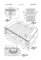
- FIG. 2 illustrates an embodiment of the present invention in which a low voltage bipolar transistor 20 includes interdigitated base, emitter and collector electrodes.
- the bipolar transistor 20 includes a semiconductor substrate 21 of a first conductivity type, such as P-type substrate.
- An epitaxial layer 22 of a second conductivity type (N-type) is formed on a major surface of the substrate 21.
- a buried layer 23 of N + conductivity type is formed at the interface of the substrate 21 and the epitaxial layer 22.
- the buried layer 23 is formed by well-known diffusion techniques.
- a deep collector contact (or sinker) region 24 of N + conductivity type extends from the surface and continues through the epitaxial layer 22 and makes contact with the buried layer 23. Also extending from the surface of the epitaxial layer and through the epitaxial layer to the substrate 21 is a P-type region 25 which completely surrounds the collector region (including the buried layer 23 and collector region 24) and isolates this portion of the epitaxial layer 22 from all other portions of the epitaxial layer. Accordingly, the semiconductor device formed within the isolation region or pocket region 26 is electrically separate and apart from other semiconductor devices which may be physically included on the same substrate.
- the voltage and current carrying capabilities of the desired device dictate, among other things, the relative thickness of the epitaxial layer and the resistivity thereof.
- the resistivity of approximately 15 ohm-cm and an epitaxial layer thickness of approximately 45 microns are useful in providing high voltage power devices.
- the fabrication of low voltage signal devices in such an epitaxial layer by prior art techniques would result in the fabrication of a transistor characterized by a high collector series resistance including the bulk collector resistance, the buried layer resistance and the deep collector contact resistance.
- the resulting low power signal semiconductor would exhibit high saturation resistance, a clearly undesirable characteristic for a transistor operated in a switching mode, where the high saturation resistance would undesirably increase power losses in the device.
- FIG. 2 illustrates this region of lower resistivity by the numeral 31, which depicts the outline of this lower resistivity region which, for example, may be formed by a closed tube or capsule diffusion technique. If it is desired to provide a low cost process, then certain technical considerations may limit the overall effectiveness of this step. For example, these deep diffusions must be weighted against the required low surface concentrations and reasonable diffusion times, including the costs associated with the diffusion times.
- the surface concentration of region 31 cannot exceed that of the P-type base diffusion chosen for the power device characteristics. Otherwise, type conversion will not occur.
- the surface concentration value for the P-type base diffusion is typically 10 18 atoms/cm 3 .
- the average resistivity near the surface is approximately 0.3 ohm-cm, but increases to the background value of resistivity (i.e., 10-12 ohm-cm).
- the average resistivity over the pocket region 31 may be approximately 1 ohm-cm.
- the depth of pocket region 31 may not extend fully to the buried layer 23. Therefore, under some conditions, there may be a region 27 of uniform resistivity formed by the unmodified epitaxial layer 22.
- a plurality of base regions 32 are formed by P-type diffusion, for example.
- the P-type base regions 32 are elongated and, as further illustrated in the plan view of FIG. 3, are interconnected by a common P-type region and by an overlying conductive grid 42.
- a first plurality of N + conductivity type regions 33 are also formed, by diffusion, for example, into the P-type base regions 32, forming the emitter region of the device.
- a second plurality of N + conductivity type regions 34 (which may be formed simultaneously with regions 33) are formed between the base regions 32 and comprise a portion of the collector region of the semiconductor device.
- the semiconductor device illustrated in FIG. 2 includes a bipolar transistor comprising a collector region including the buried layer 23, the deep collector contact region 24 and the plurality of N + -conductivity type collector regions 34 formed in the lower resistivity region 31 and interdigitated with the base regions 32.
- the surface of the epitaxial layer 22 is selectively covered with an insulating material 35, such as silicon dioxide, and a selectively patterned conductive material such as aluminum, molybdenum, polycrystalline silicon, or other suitable electrode materials.
- an insulating material 35 such as silicon dioxide
- a selectively patterned conductive material such as aluminum, molybdenum, polycrystalline silicon, or other suitable electrode materials.
- the resulting electrode configuration includes interdigitated base, emitter and collector means for making contact to the underlying semiconductor regions.
- FIG. 3 is a plan view of the embodiment of the invention illustrated in FIG. 2.
- the emitter, base and collector electrodes are designated by the reference numerals 41, 42 and 43, respectively.
- FIG. 3 illustrates only a portion of a monolithic integrated circuit including numerous other components including, for example, high voltage power transistors useful in the circuit configuration illustrated in FIG. 1.
- the total collector resistance R C is equal to the parallel combination of two resistive components, the series resistance normally associated with conventional bipolar integrated circuits, designated as R NT , and the spreading resistances associated with the regions 51, 52 and 53, illustrated in FIG. 4 and described in greater detail below.
- the resistance R NT is equal to the sum of the resistances including the R CC , the pocket region resistance, illustrated as region 51; R CE , the unmodified epitaxial collector resistance, illustrated as region 27 in FIG. 4; R BL , the lateral buried layer resistance; and R DC , the deep collector contact resistance.
- the total collector resistance R C is approximately equal to R NT shunted by a parallel resistance comprising a sum R S of the spreading resistances between alternately spaced collector and base regions, illustrated by the regions 51, 52 and 53 of FIG. 4.
- P 1 , P 2 and P 3 are equal to the resistivities of the semiconductor material in the 51, 52 and 53, respectively.
- the parallel resistance R S is equal to R 51 + (R 52 + R 53 )/2.
- the resistances associated with the deep collector contact, R DC , and buried layer, R BL are small compared to the collector region resistances R CE and R CC associated with regions 27 and 51, respectively. Furthermore, the resistance R 53 associated with regions 53 is also negligible. Accordingly, the total collector resistance R C becomes almost wholly dependent on the characteristics of regions 27, 51 and 52 and is approximated by the following equation: ##EQU1##
- the parallel resistance R S is reduced to approximately 1/10 the value associated with an unmodified collector region resistance.
- the collector region resistance is reduced to approximately 1 ohm-cm by the capsule diffusion producing the pocket region 31, the total collector resistance R C is reduced still further.
- the interdigitated base, emitter and collector structure provides low collector saturation resistance by utilizing the spreading resistance characteristics between alternately spaced collector and base contacts.
- the parallel current paths as illustrated in FIG. 4, reduce the normal series collector resistance associated with a thick collector region, a wide buried layer and a deep collector contact diffusion, necessitated by a monolithic integrated structure including both high voltage power and low voltage signal devices.
Landscapes
- Bipolar Transistors (AREA)
- Bipolar Integrated Circuits (AREA)
Priority Applications (8)
| Application Number | Priority Date | Filing Date | Title |
|---|---|---|---|
| US05/644,338 US4047220A (en) | 1975-12-24 | 1975-12-24 | Bipolar transistor structure having low saturation resistance |
| GB52026/76A GB1562735A (en) | 1975-12-24 | 1976-12-14 | Semiconductor device |
| MX167459A MX143444A (es) | 1975-12-24 | 1976-12-16 | Mejoras en transistor bipolar con baja resistencia de saturacion |
| FR7638070A FR2336800A1 (fr) | 1975-12-24 | 1976-12-17 | Structure de dispositif semi-conducteur monolithique |
| FI763629A FI66263C (fi) | 1975-12-24 | 1976-12-17 | Monolitisk halvledareanordning med laog maettnadsresistans |
| DE2658090A DE2658090C2 (de) | 1975-12-24 | 1976-12-22 | Monolithisch integrierter bipolarer Transistor mit niedrigem Sättigungswiderstand |
| IT30788/76A IT1065584B (it) | 1975-12-24 | 1976-12-23 | Struttura di transitore bipolare avente bassa resistenza di saturazione |
| JP15434676A JPS5287376A (en) | 1975-12-24 | 1976-12-23 | Monolithic semiconductor device |
Applications Claiming Priority (1)
| Application Number | Priority Date | Filing Date | Title |
|---|---|---|---|
| US05/644,338 US4047220A (en) | 1975-12-24 | 1975-12-24 | Bipolar transistor structure having low saturation resistance |
Publications (1)
| Publication Number | Publication Date |
|---|---|
| US4047220A true US4047220A (en) | 1977-09-06 |
Family
ID=24584465
Family Applications (1)
| Application Number | Title | Priority Date | Filing Date |
|---|---|---|---|
| US05/644,338 Expired - Lifetime US4047220A (en) | 1975-12-24 | 1975-12-24 | Bipolar transistor structure having low saturation resistance |
Country Status (8)
| Country | Link |
|---|---|
| US (1) | US4047220A (enExample) |
| JP (1) | JPS5287376A (enExample) |
| DE (1) | DE2658090C2 (enExample) |
| FI (1) | FI66263C (enExample) |
| FR (1) | FR2336800A1 (enExample) |
| GB (1) | GB1562735A (enExample) |
| IT (1) | IT1065584B (enExample) |
| MX (1) | MX143444A (enExample) |
Cited By (14)
| Publication number | Priority date | Publication date | Assignee | Title |
|---|---|---|---|---|
| US4117507A (en) * | 1976-06-22 | 1978-09-26 | Sgs-Ates Componeti Elettronici S.P.A. | Diode formed in integrated-circuit structure |
| US4152715A (en) * | 1977-11-28 | 1979-05-01 | The United States Of America As Represented By The Secretary Of The Army | Silicon base CCD-bipolar transistor compatible methods and products |
| US4233618A (en) * | 1978-07-31 | 1980-11-11 | Sprague Electric Company | Integrated circuit with power transistor |
| US4236164A (en) * | 1977-12-28 | 1980-11-25 | Bell Telephone Laboratories, Incorporated | Bipolar transistor stabilization structure |
| US4239558A (en) * | 1978-06-01 | 1980-12-16 | Mitsubishi Denki Kabushiki Kaisha | Method of manufacturing semiconductor devices utilizing epitaxial deposition and triple diffusion |
| US4412142A (en) * | 1980-12-24 | 1983-10-25 | General Electric Company | Integrated circuit incorporating low voltage and high voltage semiconductor devices |
| US5001538A (en) * | 1988-12-28 | 1991-03-19 | Synergy Semiconductor Corporation | Bipolar sinker structure and process for forming same |
| US5068702A (en) * | 1986-03-31 | 1991-11-26 | Exar Corporation | Programmable transistor |
| US5598018A (en) * | 1978-10-13 | 1997-01-28 | International Rectifier Corporation | High power MOSFET with low on-resistance and high breakdown voltage |
| US5723349A (en) * | 1994-01-27 | 1998-03-03 | Consorzio Pre La Ricerca Sulla Microelettronica Nel Mezzogiorno | Process for manufacturing a high conductivity insulated gate bipolar transistor integrater structure |
| US6611043B2 (en) * | 2000-03-15 | 2003-08-26 | Nec Corporation | Bipolar transistor and semiconductor device having the same |
| US20160079227A1 (en) * | 2014-03-24 | 2016-03-17 | Texas Instruments Incorporated | Esd protection circuit with plural avalanche diodes |
| US9312371B2 (en) * | 2014-07-24 | 2016-04-12 | Globalfoundries Inc. | Bipolar junction transistors and methods of fabrication |
| CN111063723A (zh) * | 2019-11-25 | 2020-04-24 | 深圳深爱半导体股份有限公司 | 开关集成控制器和三极管芯片 |
Citations (2)
| Publication number | Priority date | Publication date | Assignee | Title |
|---|---|---|---|---|
| US3460006A (en) * | 1966-02-28 | 1969-08-05 | Westinghouse Electric Corp | Semiconductor integrated circuits with improved isolation |
| US3665266A (en) * | 1970-12-10 | 1972-05-23 | Motorola Inc | Low saturation resistance,low offset voltage,monolithic analog switch |
Family Cites Families (4)
| Publication number | Priority date | Publication date | Assignee | Title |
|---|---|---|---|---|
| NL143074B (nl) * | 1963-12-13 | 1974-08-15 | Philips Nv | Transistor. |
| US3730787A (en) * | 1970-08-26 | 1973-05-01 | Bell Telephone Labor Inc | Method of fabricating semiconductor integrated circuits using deposited doped oxides as a source of dopant impurities |
| FR2144595B1 (enExample) * | 1971-07-07 | 1974-09-06 | Radiotechnique Compelec | |
| CA1056070A (en) * | 1975-02-25 | 1979-06-05 | General Electric Company | Method of making an ic structure having both power and signal components |
-
1975
- 1975-12-24 US US05/644,338 patent/US4047220A/en not_active Expired - Lifetime
-
1976
- 1976-12-14 GB GB52026/76A patent/GB1562735A/en not_active Expired
- 1976-12-16 MX MX167459A patent/MX143444A/es unknown
- 1976-12-17 FR FR7638070A patent/FR2336800A1/fr active Granted
- 1976-12-17 FI FI763629A patent/FI66263C/fi not_active IP Right Cessation
- 1976-12-22 DE DE2658090A patent/DE2658090C2/de not_active Expired
- 1976-12-23 IT IT30788/76A patent/IT1065584B/it active
- 1976-12-23 JP JP15434676A patent/JPS5287376A/ja active Granted
Patent Citations (2)
| Publication number | Priority date | Publication date | Assignee | Title |
|---|---|---|---|---|
| US3460006A (en) * | 1966-02-28 | 1969-08-05 | Westinghouse Electric Corp | Semiconductor integrated circuits with improved isolation |
| US3665266A (en) * | 1970-12-10 | 1972-05-23 | Motorola Inc | Low saturation resistance,low offset voltage,monolithic analog switch |
Cited By (19)
| Publication number | Priority date | Publication date | Assignee | Title |
|---|---|---|---|---|
| US4117507A (en) * | 1976-06-22 | 1978-09-26 | Sgs-Ates Componeti Elettronici S.P.A. | Diode formed in integrated-circuit structure |
| US4152715A (en) * | 1977-11-28 | 1979-05-01 | The United States Of America As Represented By The Secretary Of The Army | Silicon base CCD-bipolar transistor compatible methods and products |
| US4236164A (en) * | 1977-12-28 | 1980-11-25 | Bell Telephone Laboratories, Incorporated | Bipolar transistor stabilization structure |
| US4239558A (en) * | 1978-06-01 | 1980-12-16 | Mitsubishi Denki Kabushiki Kaisha | Method of manufacturing semiconductor devices utilizing epitaxial deposition and triple diffusion |
| US4233618A (en) * | 1978-07-31 | 1980-11-11 | Sprague Electric Company | Integrated circuit with power transistor |
| US5598018A (en) * | 1978-10-13 | 1997-01-28 | International Rectifier Corporation | High power MOSFET with low on-resistance and high breakdown voltage |
| US4412142A (en) * | 1980-12-24 | 1983-10-25 | General Electric Company | Integrated circuit incorporating low voltage and high voltage semiconductor devices |
| US5068702A (en) * | 1986-03-31 | 1991-11-26 | Exar Corporation | Programmable transistor |
| US5001538A (en) * | 1988-12-28 | 1991-03-19 | Synergy Semiconductor Corporation | Bipolar sinker structure and process for forming same |
| US5723349A (en) * | 1994-01-27 | 1998-03-03 | Consorzio Pre La Ricerca Sulla Microelettronica Nel Mezzogiorno | Process for manufacturing a high conductivity insulated gate bipolar transistor integrater structure |
| US6611043B2 (en) * | 2000-03-15 | 2003-08-26 | Nec Corporation | Bipolar transistor and semiconductor device having the same |
| US9997511B2 (en) * | 2014-03-24 | 2018-06-12 | Texas Instruments Incorporated | ESD protection circuit with plural avalanche diodes |
| US20160079227A1 (en) * | 2014-03-24 | 2016-03-17 | Texas Instruments Incorporated | Esd protection circuit with plural avalanche diodes |
| US9831231B2 (en) * | 2014-03-24 | 2017-11-28 | Texas Instruments Incorporated | ESD protection circuit with plural avalanche diodes |
| US9899368B2 (en) | 2014-03-24 | 2018-02-20 | Texas Instruments Incorporated | ESD protection circuit with plural avalanche diodes |
| US9312371B2 (en) * | 2014-07-24 | 2016-04-12 | Globalfoundries Inc. | Bipolar junction transistors and methods of fabrication |
| US9905668B2 (en) | 2014-07-24 | 2018-02-27 | Globalfoundries Inc. | Bipolar junction transistors and methods of fabrication |
| CN111063723A (zh) * | 2019-11-25 | 2020-04-24 | 深圳深爱半导体股份有限公司 | 开关集成控制器和三极管芯片 |
| CN111063723B (zh) * | 2019-11-25 | 2021-12-28 | 深圳深爱半导体股份有限公司 | 开关集成控制器 |
Also Published As
| Publication number | Publication date |
|---|---|
| DE2658090C2 (de) | 1985-12-12 |
| DE2658090A1 (de) | 1977-07-07 |
| FI66263B (fi) | 1984-05-31 |
| JPS5551346B2 (enExample) | 1980-12-23 |
| MX143444A (es) | 1981-05-12 |
| GB1562735A (en) | 1980-03-12 |
| FR2336800A1 (fr) | 1977-07-22 |
| FR2336800B1 (enExample) | 1982-11-05 |
| IT1065584B (it) | 1985-02-25 |
| FI66263C (fi) | 1984-09-10 |
| JPS5287376A (en) | 1977-07-21 |
| FI763629A7 (enExample) | 1977-06-25 |
Similar Documents
| Publication | Publication Date | Title |
|---|---|---|
| US4047220A (en) | Bipolar transistor structure having low saturation resistance | |
| US5089864A (en) | Insulated gate type semiconductor device | |
| JPH0758784B2 (ja) | ラッチ・アップ防止性能を改良したラテラル形絶縁ゲート・バイポーラ・トランジスタ | |
| US9455253B2 (en) | Bidirectional switch | |
| US4051506A (en) | Complementary semiconductor device | |
| US4611235A (en) | Thyristor with turn-off FET | |
| JP2766071B2 (ja) | 複合半導体装置及びそれを使つた電力変換装置 | |
| JP2001507524A (ja) | ハーフブリッジ回路を具える半導体デバイス | |
| US5185649A (en) | Circuital arrangement for preventing latchup in transistors with insulated collectors | |
| US5272363A (en) | Bidirectional protection component | |
| JPH04216674A (ja) | 横形mos制御形サイリスタ | |
| JPH025532A (ja) | pnp型の縦型孤立コレクタトランジスタ | |
| US3979766A (en) | Semiconductor device | |
| EP0064614B1 (en) | Improved emitter structure for semiconductor devices | |
| JPH0556667B2 (enExample) | ||
| US4646122A (en) | Semiconductor device with floating remote gate turn-off means | |
| JP2627330B2 (ja) | 電圧降下制御ダイオード | |
| US5998855A (en) | Bipolar power transistor with buried base and interdigitated geometry | |
| US4958210A (en) | High voltage integrated circuits | |
| EP0023130B1 (en) | Semiconductor switch | |
| JPH0328836B2 (enExample) | ||
| US4007475A (en) | Semiconductor switching device | |
| JPS6060753A (ja) | 半導体装置 | |
| JPS6327865B2 (enExample) | ||
| JP3128958B2 (ja) | 半導体集積回路 |