US9312371B2 - Bipolar junction transistors and methods of fabrication - Google Patents
Bipolar junction transistors and methods of fabrication Download PDFInfo
- Publication number
- US9312371B2 US9312371B2 US14/339,505 US201414339505A US9312371B2 US 9312371 B2 US9312371 B2 US 9312371B2 US 201414339505 A US201414339505 A US 201414339505A US 9312371 B2 US9312371 B2 US 9312371B2
- Authority
- US
- United States
- Prior art keywords
- region
- base
- collector
- regions
- emitter
- Prior art date
- Legal status (The legal status is an assumption and is not a legal conclusion. Google has not performed a legal analysis and makes no representation as to the accuracy of the status listed.)
- Expired - Fee Related
Links
- 238000004519 manufacturing process Methods 0.000 title abstract description 10
- 238000000034 method Methods 0.000 title description 20
- 239000000758 substrate Substances 0.000 claims abstract description 71
- 239000000463 material Substances 0.000 claims description 26
- 239000000969 carrier Substances 0.000 claims description 24
- 239000004020 conductor Substances 0.000 claims description 15
- 230000003071 parasitic effect Effects 0.000 claims description 14
- 238000009792 diffusion process Methods 0.000 claims description 6
- 229910021332 silicide Inorganic materials 0.000 claims description 5
- FVBUAEGBCNSCDD-UHFFFAOYSA-N silicide(4-) Chemical compound [Si-4] FVBUAEGBCNSCDD-UHFFFAOYSA-N 0.000 claims description 5
- 230000008569 process Effects 0.000 description 9
- 230000015572 biosynthetic process Effects 0.000 description 5
- 230000006870 function Effects 0.000 description 5
- 229910000577 Silicon-germanium Inorganic materials 0.000 description 4
- 238000013461 design Methods 0.000 description 4
- 238000005516 engineering process Methods 0.000 description 3
- 238000002513 implantation Methods 0.000 description 3
- 229910001218 Gallium arsenide Inorganic materials 0.000 description 2
- KDLHZDBZIXYQEI-UHFFFAOYSA-N Palladium Chemical compound [Pd] KDLHZDBZIXYQEI-UHFFFAOYSA-N 0.000 description 2
- LEVVHYCKPQWKOP-UHFFFAOYSA-N [Si].[Ge] Chemical compound [Si].[Ge] LEVVHYCKPQWKOP-UHFFFAOYSA-N 0.000 description 2
- 150000001875 compounds Chemical class 0.000 description 2
- 239000002019 doping agent Substances 0.000 description 2
- 230000000737 periodic effect Effects 0.000 description 2
- 238000012545 processing Methods 0.000 description 2
- 238000007792 addition Methods 0.000 description 1
- 230000008859 change Effects 0.000 description 1
- 238000004891 communication Methods 0.000 description 1
- 238000011161 development Methods 0.000 description 1
- 238000005530 etching Methods 0.000 description 1
- 238000012986 modification Methods 0.000 description 1
- 230000004048 modification Effects 0.000 description 1
- 229910052763 palladium Inorganic materials 0.000 description 1
- 230000006798 recombination Effects 0.000 description 1
- 238000005215 recombination Methods 0.000 description 1
- 238000006467 substitution reaction Methods 0.000 description 1
- 229910021341 titanium silicide Inorganic materials 0.000 description 1
Images


Classifications
-
- H—ELECTRICITY
- H10—SEMICONDUCTOR DEVICES; ELECTRIC SOLID-STATE DEVICES NOT OTHERWISE PROVIDED FOR
- H10D—INORGANIC ELECTRIC SEMICONDUCTOR DEVICES
- H10D12/00—Bipolar devices controlled by the field effect, e.g. insulated-gate bipolar transistors [IGBT]
- H10D12/01—Manufacture or treatment
-
- H01L29/7393—
-
- H01L29/45—
-
- H01L29/66325—
-
- H—ELECTRICITY
- H10—SEMICONDUCTOR DEVICES; ELECTRIC SOLID-STATE DEVICES NOT OTHERWISE PROVIDED FOR
- H10D—INORGANIC ELECTRIC SEMICONDUCTOR DEVICES
- H10D10/00—Bipolar junction transistors [BJT]
- H10D10/01—Manufacture or treatment
- H10D10/061—Manufacture or treatment of lateral BJTs
-
- H—ELECTRICITY
- H10—SEMICONDUCTOR DEVICES; ELECTRIC SOLID-STATE DEVICES NOT OTHERWISE PROVIDED FOR
- H10D—INORGANIC ELECTRIC SEMICONDUCTOR DEVICES
- H10D10/00—Bipolar junction transistors [BJT]
- H10D10/60—Lateral BJTs
-
- H—ELECTRICITY
- H10—SEMICONDUCTOR DEVICES; ELECTRIC SOLID-STATE DEVICES NOT OTHERWISE PROVIDED FOR
- H10D—INORGANIC ELECTRIC SEMICONDUCTOR DEVICES
- H10D12/00—Bipolar devices controlled by the field effect, e.g. insulated-gate bipolar transistors [IGBT]
- H10D12/411—Insulated-gate bipolar transistors [IGBT]
-
- H—ELECTRICITY
- H10—SEMICONDUCTOR DEVICES; ELECTRIC SOLID-STATE DEVICES NOT OTHERWISE PROVIDED FOR
- H10D—INORGANIC ELECTRIC SEMICONDUCTOR DEVICES
- H10D62/00—Semiconductor bodies, or regions thereof, of devices having potential barriers
- H10D62/10—Shapes, relative sizes or dispositions of the regions of the semiconductor bodies; Shapes of the semiconductor bodies
- H10D62/124—Shapes, relative sizes or dispositions of the regions of semiconductor bodies or of junctions between the regions
- H10D62/126—Top-view geometrical layouts of the regions or the junctions
-
- H—ELECTRICITY
- H10—SEMICONDUCTOR DEVICES; ELECTRIC SOLID-STATE DEVICES NOT OTHERWISE PROVIDED FOR
- H10D—INORGANIC ELECTRIC SEMICONDUCTOR DEVICES
- H10D64/00—Electrodes of devices having potential barriers
- H10D64/111—Field plates
-
- H—ELECTRICITY
- H10—SEMICONDUCTOR DEVICES; ELECTRIC SOLID-STATE DEVICES NOT OTHERWISE PROVIDED FOR
- H10D—INORGANIC ELECTRIC SEMICONDUCTOR DEVICES
- H10D64/00—Electrodes of devices having potential barriers
- H10D64/20—Electrodes characterised by their shapes, relative sizes or dispositions
- H10D64/23—Electrodes carrying the current to be rectified, amplified, oscillated or switched, e.g. sources, drains, anodes or cathodes
- H10D64/231—Emitter or collector electrodes for bipolar transistors
-
- H—ELECTRICITY
- H10—SEMICONDUCTOR DEVICES; ELECTRIC SOLID-STATE DEVICES NOT OTHERWISE PROVIDED FOR
- H10D—INORGANIC ELECTRIC SEMICONDUCTOR DEVICES
- H10D64/00—Electrodes of devices having potential barriers
- H10D64/60—Electrodes characterised by their materials
- H10D64/62—Electrodes ohmically coupled to a semiconductor
-
- H—ELECTRICITY
- H10—SEMICONDUCTOR DEVICES; ELECTRIC SOLID-STATE DEVICES NOT OTHERWISE PROVIDED FOR
- H10D—INORGANIC ELECTRIC SEMICONDUCTOR DEVICES
- H10D62/00—Semiconductor bodies, or regions thereof, of devices having potential barriers
- H10D62/10—Shapes, relative sizes or dispositions of the regions of the semiconductor bodies; Shapes of the semiconductor bodies
- H10D62/13—Semiconductor regions connected to electrodes carrying current to be rectified, amplified or switched, e.g. source or drain regions
- H10D62/133—Emitter regions of BJTs
- H10D62/134—Emitter regions of BJTs of lateral BJTs
-
- H—ELECTRICITY
- H10—SEMICONDUCTOR DEVICES; ELECTRIC SOLID-STATE DEVICES NOT OTHERWISE PROVIDED FOR
- H10D—INORGANIC ELECTRIC SEMICONDUCTOR DEVICES
- H10D62/00—Semiconductor bodies, or regions thereof, of devices having potential barriers
- H10D62/10—Shapes, relative sizes or dispositions of the regions of the semiconductor bodies; Shapes of the semiconductor bodies
- H10D62/13—Semiconductor regions connected to electrodes carrying current to be rectified, amplified or switched, e.g. source or drain regions
- H10D62/137—Collector regions of BJTs
Definitions
- the present invention generally relates to fabricating circuit structures, and more specifically, to bipolar junction transistors and methods of fabrication thereof.
- circuit structures capable of high performance and low power consumption for a wide variety of applications.
- circuit structures may be manufactured at low cost using inexpensive materials and using established, cost-effective manufacturing tools and techniques. These objectives continue to drive innovation in the development of energy-efficient, high-speed circuit structures, as well as processes for fabricating such circuit structures.
- a structure including a bipolar junction transistor which includes: a substrate including a substrate region having a first conductivity type; an emitter region over a first portion of the substrate region, the emitter region having a second conductivity type; a collector region over a second portion of the substrate region, the collector region having the second conductivity type; and, a base region overlie structure disposed over, in part, the substrate region, the base region overlie structure separating the emitter region from the collector region and aligning to a base region of the bipolar junction transistor within the substrate region between the first portion and the second portion thereof.
- a method of fabricating a bipolar junction transistor in which the fabricating includes: providing a substrate including a substrate region having a first conductivity type; providing a base region overlie structure over at least a portion of the substrate region, the base region overlie structure being aligned to a base region portion of the substrate region; forming an emitter region of a second conductivity type in a first portion of the substrate region and a collector region of the second conductivity type in a second portion of the substrate region, the first and second portions being disposed on opposing sides of the base region overlie structure; and, wherein the base region overlie structure masks the base region during the forming of the emitter region and the collector region.
- FIG. 1A depicts a cross-sectional view of one embodiment of a bipolar junction transistor structure, in accordance with one or more aspects of the present invention
- FIG. 1B depicts a cross-sectional view of another embodiment of the bipolar junction transistor structure of FIG. 1A , illustrating additional features of the structure that may be included to facilitate operation of the bipolar junction transistor at low voltages and reduce parasitic resistances and capacitances in the structure, in accordance with one or more aspects of the present invention
- FIG. 1C depicts a top-down view of another embodiment of the bipolar junction transistor structure of FIG. 1A , illustrating further elements that may be included in the structure to facilitate operation of the bipolar junction transistor at low voltage and reduce parasitic resistances and capacitances in the structure, in accordance with one or more aspects of the present invention
- FIG. 1D is an isometric cross-sectional view of one embodiment of the bipolar junction transistor structure of FIG. 1C , further illustrating elements depicted in FIG. 1C , in accordance with one or more aspects of the present invention
- FIGS. 2A-2B depict top-down views of embodiments of alternative contact arrangements that may be used in conjunction with the bipolar junction transistor structures described herein, in accordance with one or more aspects of the present invention
- FIG. 3 depicts a top-down view of one embodiment of another alternative contact arrangement that may be used in conjunction with the bipolar junction transistor structures described herein, in accordance with one or more aspects of the present invention.
- FIG. 4 illustrates one embodiment of a method of forming a bipolar junction transistor, in accordance with one or more aspects of the present invention.
- RF circuit structures capable of high performance and speed at low power (low voltage) consumption.
- many mobile technologies make use of radio-frequency (RF) circuit structures for a wide range of applications, such as low-noise amplifiers, high output amplifiers, mixers, drivers, oscillators, frequency multipliers, and so on.
- RF circuit structures are designed to receive a low power signal or low input current and output an amplified signal or current.
- Bipolar junction transistors or “bipolars”
- bipolars which use a small input current to drive a large output current, may thus be well suited for some RF applications.
- designs of many bipolars are not without drawbacks.
- some bipolars may operate only at high voltages (and thus high power consumption) to generate high output currents, and may have relatively long turn-on and turn-off times compared to other circuit structures, such as MOSFETs, resulting in additional power losses.
- some bipolar designs may introduce high parasitic capacitances or parasitic resistances within the transistor, which may increase power losses as well as slower performance of the transistor. Designing RF circuit structures to resolve one or more of these issues generally introduces high manufacturing costs, whether due to expenses in materials, expenses in processing, increased fabrication time or a combination of cost factors.
- a structure including a bipolar junction transistor designed to resolve one or more of the issues described above including: a substrate including a substrate region having a first conductivity type; an emitter region over a first portion of the substrate region, the emitter region having a second conductivity type; a collector region over a second portion of the substrate region, the collector region having the second conductivity type; and, a base region overlie structure disposed over, in part, the substrate region, the base region overlie structure separating the emitter region from the collector region and aligning to a base region of the bipolar junction transistor within the substrate region between the first portion and the second portion thereof.
- a method of fabricating a bipolar junction transistor in which the fabricating includes: providing a substrate including a substrate region having a first conductivity type; providing a base region overlie structure over at least a portion of the substrate region, the base region overlie structure being aligned to a base region portion of the substrate region; forming an emitter region of a second conductivity type in a first portion of the substrate region and a collector region of the second conductivity type in a second portion of the substrate region, the first and second portions being disposed on opposing sides of the base region overlie structure; and, wherein the base region overlie structure masks the base region during the forming of the emitter region and the collector region.
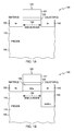
- FIG. 1A is a cross-sectional view of a portion of one embodiment of a bipolar junction transistor 100 , in accordance with one or more aspects of the present invention.
- Bipolar junction transistor 100 includes a substrate 105 and a substrate region 110 over the substrate, the substrate region 110 having a first conductivity type. As illustrated by FIG. 1A , the first conductivity type of substrate region 110 may be P-type.
- a base overlie structure 120 may be provided and disposed over, in part, substrate region 110 and aligned to a base region 150 of bipolar junction transistor 100 .
- Base overlie structure 120 may include, for example, a dielectric layer 122 and a conductive material layer 121 disposed over the dielectric layer 122 .
- Bipolar junction transistor 100 also includes an emitter region 130 over a first portion of substrate region 110 and a collector region 140 over a second portion of substrate region 110 , the first portion and second portion having a second conductivity type. As illustrated by FIG. 1A , the second conductivity type may be N-type or a similar conductivity type, such as N+ type. In an exemplary embodiment, bipolar junction transistor 100 may be a lateral NPN bipolar transistor, as described above and as illustrated by FIG. 1A . Alternatively, emitter region 130 and collector region 140 may be P-type or P+ type and base region 150 may be N-type.
- a lateral NPN bipolar transistor may allow for greater current flow from emitter 130 and collector 140 through base region 150 , and thus may also allow for faster operation and performance of bipolar junction transistor 100 .
- emitter region 130 and collector region 140 may be formed on opposing sides of base overlie structure 120 , and base overlie structure 120 may align over and mask base region 150 during formation of emitter region 130 and collector region 140 .
- emitter region 130 and collector region 140 may be formed by implantation of a doping material in the first region 130 and second region 140 , the doping material having the second conductivity type.
- Base overlie structure 120 may mask base region 150 to prevent implantation of the dopant in the base region 150 and preserve the first conductivity type in the base region 150 .
- Base overlie structure 120 may thus be self-aligned with base region 150 to separate emitter region 130 from collector region 140 , and a width of base overlie structure 120 may define a width of base region 150 .
- the process used to form base overlie structure 120 may be controlled to form base overlie structure 120 at the smallest size achievable for the process, and thus controlled to form base region 150 at the smallest width possible.
- base overlie structure 120 may be in the range 5-50 nm wide, so that base region 150 has a corresponding width of 5-50 nm.
- a bipolar junction transistor's performance depends, in part, on the size of base region 150 as a larger base region increases the likelihood that electrical carriers (e.g., electrons for N or N+ type regions) diffusing out of the emitter will undesirably recombine with the majority carriers (e.g., holes for P type regions) of the base region before diffusing into the collector region, thus reducing the net collector current obtained.
- Forming a narrow base region 150 using base overlie structure 120 may thus reduce the number of carriers diffusing out of emitter region 130 that recombine within base region 150 , thus maximizing the obtained collector current through collector 140 .
- dielectric layer 122 may be a first dielectric layer
- base overlie structure 120 may also include a second dielectric layer over conductive material layer 121 ; the first dielectric layer and second dielectric layer may electrically isolate conductive material layer 121 .
- conductive material layer 121 may include an electrical charge, the charge being selected to facilitate operation of bipolar junction transistor 100 at low voltage.
- the electrical charge on conductive material layer 121 may, for example, provide an initial voltage between base region 150 and emitter region 130 .
- the initial voltage may be below threshold voltage needed to switch the bipolar junction transistor “on,” so that the charge on conductive material layer 121 does not continually drive current through the transistor.
- additional voltage is applied to one or more base contacts (described herein below)
- the initial voltage and additional voltage together may act to turn the bipolar transistor on and drive electrical carrier diffusion from emitter 130 to collector 140 .
- the additional voltage applied to one or more base contacts may thus be relatively low compared to the net voltage required to operate the bipolar junction transistor, allowing for low voltage operation of the bipolar junction transistor.
- Low voltage operation of the bipolar junction transistor may, for example, improve low power performance of the transistor in, for instance, RF applications.
- the electrical charge of the conductive material layer may be a fixed electrical charge.
- the charge of the conductive material layer may be dynamically selected or altered to facilitate low-voltage operation of bipolar junction transistor 100 .
- FIG. 1B depicts bipolar junction transistor 100 of FIG. 1A with additional elements that may be included in one or more alternative embodiments, the additional elements being optionally included to further improve the performance of and/or facilitate operation of bipolar junction transistor at low voltage.
- the performance of a bipolar junction transistor may be measured according to the gain in collector current obtained. Maximizing collector current may not only depend in part on minimizing the width of the base region, as described above, but may also depend on minimizing parasitic resistances and parasitic capacitances within the bipolar junction transistor. This may include, for example, minimizing resistance within the base region, minimizing resistance of the collector region, reducing parasitic capacitance between the base region and emitter region, and so on. Reducing or eliminating sources of parasitic resistances and parasitic capacitances may improve the speed and performance of the bipolar junction transistor, and may also further facilitate operation of the bipolar junction transistor at low voltages.
- bipolar junction transistor 100 may include a well region 145 within substrate region 110 below collector region 140 , in which well region 145 has the second conductivity type.
- well region 145 may be N-type if collector region 140 is N-type or N+ type, as depicted in FIG. 1B .
- Well region 145 may be provided below collector region 140 to increase an effective size of the collector of bipolar junction transistor 100 , resulting in lower electrical resistance in collector region 140 .
- Well region 145 may be formed, in one instance, by etching a trench in a portion of substrate region 110 followed by filling the trench with a doped material having the second conductivity type.
- Well region 145 may be formed, in another instance, by deep implantation of a dopant material into a portion of substrate region 110 over which collector region 140 is to be formed. It may be understood that well region 145 having the second conductivity type need not be confined to a region immediately below collector 140 . In alternative embodiments, well region 145 may extend within substrate region 110 beyond the region directly below collector 140 , and may extend not only vertically within substrate region 110 (as depicted by FIG. 1A ) but also laterally within substrate region 110 .
- base region 150 may include a material 155 with a strained lattice structure, such as silicon-germanium (SiGe), as depicted in FIG. 1B , or a periodic III-IV compound such as GaAs. It may be understood that other materials may alternatively be used to form a base region 150 with a strained lattice structure.
- the strained lattice structure of material 155 may be advantageously selected to increase the mobility of electrical carriers within base region 150 , with the increased electrical carrier mobility facilitating diffusion of electrical carriers from emitter 130 through base region 150 into collector 140 during operation of bipolar junction transistor 100 .
- the electrical carriers are electrons that diffuse out of emitter 130 through base region 150 , and because base region 150 is P type, in which the majority carriers are holes, the electrons diffusing through base region 150 may undesirably recombine with holes in base region 150 and thus may not reach collector 140 .
- the electrical carriers may more quickly reach collector 140 without recombining within base region 150 .
- a base region 150 including a material 155 with a strained lattice structure may be formed by providing a substrate 105 with a substrate region 110 having a first lattice structure and a first lattice spacing, removing at least the portion of substrate region 110 to be defined as base region 150 to form a trench, and growing material 155 in the trench, in which material 155 has a second lattice structure and second lattice spacing different from the first lattice structure and spacing.
- the portion of substrate region 110 removed may be removed, for example, by a lithographic etch process.
- Growing material 155 in the trench may include, for example, an epitaxial growth process.
- material 155 may conform to the first lattice spacing and first lattice structure of substrate region 110 . Due to the difference in sizes between the first lattice spacing and the second lattice spacing, the material 155 may acquire a strained lattice structure through conforming to the first lattice spacing and first lattice structure.
- bipolar junction transistor 100 may include an oxide layer 115 below substrate region 110 .
- Oxide layer 115 may underlie, at least in part, emitter region 130 and/or collector region 140 , and/or base region 150 .
- Oxide layer 115 may be included to reduce parasitic capacitance that may arise between one or more components of bipolar junction transistor 100 , such as emitter region 130 or base region 150 , and substrate 105 or substrate region 110 .
- FIGS. 1C and 1D further illustrate additional elements and features that may be included in one or more embodiments of bipolar junction transistor 100 .
- FIG. 1C depicts a top-down view of one embodiment of bipolar junction transistor 100
- FIG. 1D is an isometric cross-sectional view of a portion of bipolar junction transistor 100 depicted by FIG. 1C , furthering illustrating additional elements that may be included in bipolar junction transistor 100 to further improve performance and/or facilitate low-voltage operation.
- bipolar junction transistor 100 may include a plurality of base contacts 180 electrically contacting substrate region 110 .
- a first base contact of the plurality of base contacts 180 may be disposed adjacent to a first end of the base region 150 (below base overlie structure 120 , not depicted in FIG. 1C ) and a second base contact of the plurality of base contacts 180 may be disposed adjacent a second end of the base region 150 .
- the plurality of base contacts 180 may advantageously minimize electrical contact resistance to base region 150 , as the plurality of base contacts effectively increases a contact area between plurality of base contacts 180 and base region 150 , allowing electrical carriers to flow at lower resistance. Consequently, lowering the resistance within base region 150 facilitates operation of bipolar junction transistor at a proportionally lower voltage.
- the plurality of base contacts may include a material with a strained lattice structure, such as silicon-germanium (SiGe) or a periodic III-IV compound such as GaAs. It may be understood that other materials may alternatively be used to form a base contacts 180 with a strained lattice structure.
- the strained lattice structure of base contacts 180 may be advantageously selected to increase the mobility of electrical carriers through base contacts 180 and base region 150 , resulting in an increased flow of majority electrical carriers from base region 150 into emitter region 130 .
- bipolar junction transistor 100 may include at least one emitter contact 160 over emitter region 130 and at least one collector contact 170 over collector region 140 .
- the at least one emitter contact 160 and at least one collector contact 170 may, in one instance, include a silicide material, such as palladium silicide or titanium silicide.
- a silicide emitter contact 160 and collector contact 170 may be formed, for example, via a silicidation process.
- a silicide material may have a low electrical resistivity compared to other electrical contact materials, and thus may facilitate lowering electrical resistance within emitter region 130 and collector region 140 .
- emitter region 130 may be one emitter region of a plurality of emitter regions 130
- collector region 140 may be one collector region of a plurality of collector regions 140
- the plurality of emitter regions 130 may, in one example, be a plurality of emitter regions formed in the upper portions of a plurality of fin structures that have been formed in substrate region 110
- the plurality of collector regions 140 may, in one example, be a plurality of collector regions formed in the upper portions of a plurality of fin structures formed in substrate region 110 .
- the plurality of fin structures may, for example, be formed in substrate region 110 at the same time in a single process, so that the resulting plurality of emitters 130 and plurality of collectors 140 are aligned with each other and separated by base overlie structure 120 .
- Base overlie structure may 120 , in one example, mask base region 150 during formation of a plurality of fin structures.
- base overlie structure 120 may be provided following formation of the plurality of fin structures and prior to formation of the plurality of emitter regions 130 and plurality of collector regions 140 .
- the plurality of collector regions 140 may further be in contact with one well region 145 , as depicted in FIG. 1C .
- a plurality of well regions 145 may be formed below the plurality of collector regions 140 , the plurality of well regions 145 being aligned with the plurality of collector regions 140 .
- the at least one emitter contact 160 may be in electrical contact with the plurality of emitter regions 130
- the at least one collector contact 170 may be in electrical contact with the plurality of collector regions 140 , as depicted in FIG. 1C and also depicted in FIG. 1D .
- the plurality of emitter regions 130 may effectively be controlled as a single emitter of bipolar junction transistor 100
- connecting the plurality of collector regions 140 with the at least one collector contact 170 may effectively control the plurality of collector regions 140 as a single collector of bipolar junction transistor 100 .
- forming a plurality of emitter regions 130 and a plurality of collector regions 140 may increase the gain (i.e., the ratio of the collector current to the base current) of bipolar junction transistor 100 .
- each of the plurality of emitter regions 130 and plurality of collector regions 140 forms a narrow interface junction with base region 150 .
- electrical carriers in one of the plurality of emitter regions 130 i.e., electrons
- the number and size of the plurality of emitter regions 130 and collector regions 140 may be selected, depending on design requirements of the circuit structure and materials used in forming substrate region 110 and emitter region 130 and collector region 140 , to optimize the gain of bipolar junction transistor 100 while maintaining low parasitic resistance in base region 150 .
- FIGS. 1C-1D illustrate just one possible arrangement of contacts for a bipolar junction transistor according to structures and methods disclosed herein.
- Embodiments of bipolar junction transistor structures disclosed herein, or alternative embodiments thereof, may allow for or be adapted to many alternative contact arrangements, according to specific design requirements for circuit structures intended for particular applications.
- FIG. 2A depicts one embodiment of an arrangement of contacts for a bipolar junction transistor 200 as disclosed herein.
- at least one emitter contact 220 may be arranged intermediate a plurality of base contacts 240 , the base contacts being in electrical contact with substrate region 210 .
- Base contacts 240 may be arranged to parallel the at least one emitter contact 220 , and at least one emitter contact 220 may be arranged parallel to or perpendicular to an emitter region or a plurality of emitter regions (not depicted in FIG. 2A ), according to one or more embodiments of a bipolar junction transistor as described herein.
- Collector contact 230 may be larger than base contacts 240 and emitter contact 230 , and may be arranged to at least partially encircle plurality of base contacts 240 and at least one emitter contact 220 , as depicted by the example in FIG. 2A .
- a larger collector contact 230 that at least partially encircles base contacts 240 and emitter contact 220 may, in one example, be in electrical contact with a collector region or well region below the collector region, where the collector region and/or well region are similarly configured to partially encircle a base region and emitter region.
- a collector region larger than the base region may facilitate increasing the gain of the bipolar junction transistor, as the larger collector region may collect stray electrical carriers that diffuse out of the emitter region but do not travel in a straight path through the base region.
- the plurality of base contacts 240 may also be a plurality of base overlie structures 120 , as described herein above in FIGS. 1A-1D ; thus, in at least one example embodiment, the base overlie structure may also function as a base contact 240 .
- FIG. 2B depicts one possible alternative embodiment of an arrangement of contacts similar to the arrangement of contacts depicted in FIG. 2A , in which additional base contacts 240 and a plurality of emitter contacts 220 are arranged in parallel with each other, along with collector contact 230 .
- Including multiple base contacts 240 and multiple emitter contacts 220 may further reduce parasitic resistances in the base region of the bipolar junction transistor, and thus may further facilitate increasing the gain of the transistor structure as well as facilitate operation of the bipolar junction transistor at low voltages.
- FIG. 3 depicts yet another embodiment of an arrangement of contacts for a bipolar junction transistor 300 as disclosed herein.
- the contact arrangement depicted in FIG. 3 may be ideal, for example, for RF bipolar junction circuit structures.
- Emitter contact 320 may be fully encircled by collector contact 330 as well as base contact 340 and the base region underlying base contact 340 .
- the contact arrangement depicted may facilitate collection of electrical carriers by collector contact 330 , as electrical carriers diffusing through the base region may not travel along a diffusion path that does not end at collector contact 330 .
- base contact 340 may also be the base overlie structure 120 , described herein above and depicted in FIGS. 1A-1D ; thus, in at least one example embodiment, the base overlie structure may also function as a base contact 340 .
- FIG. 4 depicts, by way of summary, one embodiment of a method of forming a circuit structure, the method including fabrication of a bipolar junction transistor, in accordance with one or more aspects of the present invention.
- the process may include, for example, providing a substrate including a substrate region having a first conductivity type 410 .
- the first conductivity type may, for instance, be P-type.
- a base region overlie structure may be provided over at least a portion of the substrate region, the base region overlie structure being aligned to a base region portion of the substrate region 420 .
- Providing the base region overlie structure may include, in one example, providing a dielectric layer over the substrate region and providing a conductive material layer over the dielectric layer.
- An emitter region of a second conductivity type may be formed in a first portion of the substrate region, and a collector region of the second conductivity type may be formed in a second portion of the substrate region 430 .
- the first and second portions may be disposed on opposing sides of the base region overlie structure, and the base overlie structure may mask the base region in the substrate region during formation of the emitter region and the collector region.
- the second conductivity type may, for instance, be N-type.
- Approximating language may be applied to modify any quantitative representation that could permissibly vary without resulting in a change in the basic function to which it is related. Accordingly, a value modified by a term or terms, such as “about,” is not limited to the precise value specified. In some instances, the approximating language may correspond to the precision of an instrument for measuring the value.
- a method or device that “comprises,” “has,” “includes” or “contains” one or more steps or elements possesses those one or more steps or elements, but is not limited to possessing only those one or more steps or elements.
- a step of a method or an element of a device that “comprises,” “has,” “includes” or “contains” one or more features possesses those one or more features, but is not limited to possessing only those one or more features.
- the terms “may” and “may be” indicate a possibility of an occurrence within a set of circumstances; a possession of a specified property, characteristic or function; and/or qualify another verb by expressing one or more of an ability, capability, or possibility associated with the qualified verb. Accordingly, usage of “may” and “may be” indicates that a modified term is apparently appropriate, capable, or suitable for an indicated capacity, function, or usage, while taking into account that in some circumstances the modified term may sometimes not be appropriate, capable or suitable. For example, in some circumstances, an event or capacity can be expected, while in other circumstances the event or capacity cannot occur—this distinction is captured by the terms “may” and “may be.”
Landscapes
- Bipolar Transistors (AREA)
Abstract
Description
Claims (13)
Priority Applications (2)
| Application Number | Priority Date | Filing Date | Title |
|---|---|---|---|
| US14/339,505 US9312371B2 (en) | 2014-07-24 | 2014-07-24 | Bipolar junction transistors and methods of fabrication |
| US15/057,791 US9905668B2 (en) | 2014-07-24 | 2016-03-01 | Bipolar junction transistors and methods of fabrication |
Applications Claiming Priority (1)
| Application Number | Priority Date | Filing Date | Title |
|---|---|---|---|
| US14/339,505 US9312371B2 (en) | 2014-07-24 | 2014-07-24 | Bipolar junction transistors and methods of fabrication |
Related Child Applications (1)
| Application Number | Title | Priority Date | Filing Date |
|---|---|---|---|
| US15/057,791 Division US9905668B2 (en) | 2014-07-24 | 2016-03-01 | Bipolar junction transistors and methods of fabrication |
Publications (2)
| Publication Number | Publication Date |
|---|---|
| US20160027905A1 US20160027905A1 (en) | 2016-01-28 |
| US9312371B2 true US9312371B2 (en) | 2016-04-12 |
Family
ID=55167372
Family Applications (2)
| Application Number | Title | Priority Date | Filing Date |
|---|---|---|---|
| US14/339,505 Expired - Fee Related US9312371B2 (en) | 2014-07-24 | 2014-07-24 | Bipolar junction transistors and methods of fabrication |
| US15/057,791 Active 2034-09-15 US9905668B2 (en) | 2014-07-24 | 2016-03-01 | Bipolar junction transistors and methods of fabrication |
Family Applications After (1)
| Application Number | Title | Priority Date | Filing Date |
|---|---|---|---|
| US15/057,791 Active 2034-09-15 US9905668B2 (en) | 2014-07-24 | 2016-03-01 | Bipolar junction transistors and methods of fabrication |
Country Status (1)
| Country | Link |
|---|---|
| US (2) | US9312371B2 (en) |
Cited By (1)
| Publication number | Priority date | Publication date | Assignee | Title |
|---|---|---|---|---|
| US10665702B2 (en) | 2017-12-27 | 2020-05-26 | Samsung Electronics Co., Ltd. | Vertical bipolar transistors |
Families Citing this family (8)
| Publication number | Priority date | Publication date | Assignee | Title |
|---|---|---|---|---|
| EP3324442A1 (en) * | 2016-11-21 | 2018-05-23 | Nexperia B.V. | Vertical bipolar transistor with integrated collector resistor |
| US10014397B1 (en) * | 2016-12-19 | 2018-07-03 | Globalfoundries Inc. | Bipolar junction transistors with a combined vertical-lateral architecture |
| US11094806B2 (en) * | 2017-12-29 | 2021-08-17 | Texas Instruments Incorporated | Fabricating transistors with implanting dopants at first and second dosages in the collector region to form the base region |
| US11133397B2 (en) | 2019-06-04 | 2021-09-28 | Globalfoundries U.S. Inc. | Method for forming lateral heterojunction bipolar devices and the resulting devices |
| US11276770B2 (en) | 2019-11-05 | 2022-03-15 | Globalfoundries U.S. Inc. | Gate controlled lateral bipolar junction/heterojunction transistors |
| US11152496B2 (en) | 2020-01-30 | 2021-10-19 | Globalfoundries U.S. Inc. | IC structure base and inner E/C material on raised insulator, and methods to form same |
| US11837460B2 (en) | 2021-09-03 | 2023-12-05 | Globalfoundries U.S. Inc. | Lateral bipolar transistor |
| US20250221014A1 (en) * | 2023-12-29 | 2025-07-03 | Texas Instruments Incorporated | Bipolar transistor reverse recovery |
Citations (14)
| Publication number | Priority date | Publication date | Assignee | Title |
|---|---|---|---|---|
| US4047220A (en) * | 1975-12-24 | 1977-09-06 | General Electric Company | Bipolar transistor structure having low saturation resistance |
| US6169300B1 (en) * | 1997-03-11 | 2001-01-02 | Sgs-Thomson Microelectronics S.R.L. | Insulated gate bipolar transistor with high dynamic ruggedness |
| US6423603B2 (en) * | 1998-11-06 | 2002-07-23 | International Business Machines Corporation | Method of forming a microwave array transistor for low-noise and high-power applications |
| US6469366B1 (en) * | 2000-04-27 | 2002-10-22 | Mitsubishi Denki Kabushiki Kaisha | Bipolar transistor with collector diffusion layer formed deep in the substrate |
| US20030052387A1 (en) * | 2000-01-31 | 2003-03-20 | Josef Boeck | Bipolar transistor |
| US20050056827A1 (en) * | 2003-09-15 | 2005-03-17 | Agency For Science, Technology And Research | CMOS compatible low band offset double barrier resonant tunneling diode |
| US20120068309A1 (en) * | 2010-09-22 | 2012-03-22 | Klaus Diefenbeck | Transistor and Method of Manufacturing a Transistor |
| US20120098096A1 (en) * | 2010-10-21 | 2012-04-26 | Freescale Semiconductor, Inc. | bipolar transistor |
| US20130146978A1 (en) * | 2011-12-08 | 2013-06-13 | Texas Instruments Incorporated | Transistor assisted esd diode |
| US20130299944A1 (en) * | 2012-05-14 | 2013-11-14 | Taiwan Semiconductor Manufacturing Company, Ltd. | Methods and Apparatus for Bipolar Junction Transistors and Resistors |
| US20130313571A1 (en) * | 2011-01-31 | 2013-11-28 | Fairchild Semiconductor Corporation | Silicon carbide bipolar junction transistor comprising shielding regions and methods of manufacturing the same |
| US20140117451A1 (en) * | 2012-10-30 | 2014-05-01 | Seiko Instruments Inc. | Semiconductor device |
| US20140239451A1 (en) * | 2013-02-26 | 2014-08-28 | Broadcom Corporation | Semiconductor Devices Including A Lateral Bipolar Structure And Fabrication Methods |
| US20140291765A1 (en) * | 2013-03-28 | 2014-10-02 | Semiconductor Manufacturing International (Shanghai) Corporation | Esd protection structure and esd protection circuit |
Family Cites Families (2)
| Publication number | Priority date | Publication date | Assignee | Title |
|---|---|---|---|---|
| WO2004056181A1 (en) | 2002-12-23 | 2004-07-08 | Global Cardiac Solutions Pty Ltd | Organ preconditioning, arrest, protection, preservation and recovery (2) |
| US8258602B2 (en) * | 2009-01-28 | 2012-09-04 | Taiwan Semiconductor Manufacturing Company, Ltd. | Bipolar junction transistors having a fin |
-
2014
- 2014-07-24 US US14/339,505 patent/US9312371B2/en not_active Expired - Fee Related
-
2016
- 2016-03-01 US US15/057,791 patent/US9905668B2/en active Active
Patent Citations (14)
| Publication number | Priority date | Publication date | Assignee | Title |
|---|---|---|---|---|
| US4047220A (en) * | 1975-12-24 | 1977-09-06 | General Electric Company | Bipolar transistor structure having low saturation resistance |
| US6169300B1 (en) * | 1997-03-11 | 2001-01-02 | Sgs-Thomson Microelectronics S.R.L. | Insulated gate bipolar transistor with high dynamic ruggedness |
| US6423603B2 (en) * | 1998-11-06 | 2002-07-23 | International Business Machines Corporation | Method of forming a microwave array transistor for low-noise and high-power applications |
| US20030052387A1 (en) * | 2000-01-31 | 2003-03-20 | Josef Boeck | Bipolar transistor |
| US6469366B1 (en) * | 2000-04-27 | 2002-10-22 | Mitsubishi Denki Kabushiki Kaisha | Bipolar transistor with collector diffusion layer formed deep in the substrate |
| US20050056827A1 (en) * | 2003-09-15 | 2005-03-17 | Agency For Science, Technology And Research | CMOS compatible low band offset double barrier resonant tunneling diode |
| US20120068309A1 (en) * | 2010-09-22 | 2012-03-22 | Klaus Diefenbeck | Transistor and Method of Manufacturing a Transistor |
| US20120098096A1 (en) * | 2010-10-21 | 2012-04-26 | Freescale Semiconductor, Inc. | bipolar transistor |
| US20130313571A1 (en) * | 2011-01-31 | 2013-11-28 | Fairchild Semiconductor Corporation | Silicon carbide bipolar junction transistor comprising shielding regions and methods of manufacturing the same |
| US20130146978A1 (en) * | 2011-12-08 | 2013-06-13 | Texas Instruments Incorporated | Transistor assisted esd diode |
| US20130299944A1 (en) * | 2012-05-14 | 2013-11-14 | Taiwan Semiconductor Manufacturing Company, Ltd. | Methods and Apparatus for Bipolar Junction Transistors and Resistors |
| US20140117451A1 (en) * | 2012-10-30 | 2014-05-01 | Seiko Instruments Inc. | Semiconductor device |
| US20140239451A1 (en) * | 2013-02-26 | 2014-08-28 | Broadcom Corporation | Semiconductor Devices Including A Lateral Bipolar Structure And Fabrication Methods |
| US20140291765A1 (en) * | 2013-03-28 | 2014-10-02 | Semiconductor Manufacturing International (Shanghai) Corporation | Esd protection structure and esd protection circuit |
Non-Patent Citations (4)
| Title |
|---|
| Chu, "Bipolar Transistor", ch08vc.fm, Friday, Feb. 13, 2009, 34 pages. |
| Hasler et al., "Floating-Gate Devices, Circuits, and Systems", 9th International Database Engineering & Application Symposium (IDEAS 2005), Atlanta, Georga, 6 pages. |
| Jaeger, "Introduction to Microelectronic Fabrication", vol. 5, Second Edition, Prentice Hall, Upper Saddle River, New Jersey 07458 (2002), 14 pages. |
| NXP Product Information Page-Transistors for any RF function, downloaded Jul. 22, 2014, http://www.nxp.com/products/rf/transistors/bipolar/lnas-mixers-frequency-multipliers-buffers/3-5-ghz-gt-6-ghz-s-c-band/, 2 pages. |
Cited By (1)
| Publication number | Priority date | Publication date | Assignee | Title |
|---|---|---|---|---|
| US10665702B2 (en) | 2017-12-27 | 2020-05-26 | Samsung Electronics Co., Ltd. | Vertical bipolar transistors |
Also Published As
| Publication number | Publication date |
|---|---|
| US20160181393A1 (en) | 2016-06-23 |
| US20160027905A1 (en) | 2016-01-28 |
| US9905668B2 (en) | 2018-02-27 |
Similar Documents
| Publication | Publication Date | Title |
|---|---|---|
| US9905668B2 (en) | Bipolar junction transistors and methods of fabrication | |
| US8310027B2 (en) | Electronic device and manufacturing method thereof | |
| JP4524298B2 (en) | Manufacturing method of semiconductor device | |
| US6770952B2 (en) | Integrated process for high voltage and high performance silicon-on-insulator bipolar devices | |
| EP2168163B1 (en) | Junction field effect transistor with a hyperabrupt junction | |
| CN102299151B (en) | There is the semiconductor device of heterojunction bipolar transistor and field-effect transistor | |
| US7709311B1 (en) | JFET device with improved off-state leakage current and method of fabrication | |
| CN112670349B (en) | Solid source diffusion junctions for fin-based electronic devices | |
| US9780003B2 (en) | Bipolar junction transistor formed on fin structures | |
| EP2497117B1 (en) | Junction field effect transistor and method of manufacturing the same | |
| CN107068734A (en) | One kind is without junction field effect transistor | |
| KR101716957B1 (en) | Junction gate field-effect transistor (jfet), semiconductor device and method of manufacturing | |
| US8004058B2 (en) | Schottky diode for high speed and radio frequency application | |
| JP4608205B2 (en) | Bipolar transistor with majority carrier storage layer as subcollector | |
| JPWO2008123491A1 (en) | Semiconductor device using carrier multiplication by ionizing collision and method for manufacturing the same | |
| US8866189B2 (en) | Silicon-germanium heterojunction bipolar transistor and manufacturing method thereof | |
| US8581339B2 (en) | Structure of NPN-BJT for improving punch through between collector and emitter | |
| US9054181B2 (en) | Semiconductor device, integrated circuit and method of manufacturing a semiconductor device | |
| JP2010183054A (en) | Heterojunction bipolar transistor and method of manufacturing the same | |
| US20240363742A1 (en) | Transistor feedback capacitance reduction | |
| US8829650B2 (en) | Zener diode in a SiGe BiCMOS process and method of fabricating the same | |
| JP2010287603A (en) | Compound semiconductor device and manufacturing method thereof | |
| KR20180074014A (en) | Vertical nanowire tunneling field-effect transistor and method for fabricating the same | |
| CN116525675A (en) | Vertical Fin-Based Field Effect Transistor with Neutral Fin Top | |
| JP2011035197A (en) | Field effect transistor, manufacturing method of field effect transistor, and communication device |
Legal Events
| Date | Code | Title | Description |
|---|---|---|---|
| AS | Assignment |
Owner name: GLOBALFOUNDRIES INC., CAYMAN ISLANDS Free format text: ASSIGNMENT OF ASSIGNORS INTEREST;ASSIGNOR:SINGH, JAGAR;REEL/FRAME:033380/0527 Effective date: 20140717 |
|
| STCF | Information on status: patent grant |
Free format text: PATENTED CASE |
|
| AS | Assignment |
Owner name: WILMINGTON TRUST, NATIONAL ASSOCIATION, DELAWARE Free format text: SECURITY AGREEMENT;ASSIGNOR:GLOBALFOUNDRIES INC.;REEL/FRAME:049490/0001 Effective date: 20181127 |
|
| FEPP | Fee payment procedure |
Free format text: MAINTENANCE FEE REMINDER MAILED (ORIGINAL EVENT CODE: REM.); ENTITY STATUS OF PATENT OWNER: LARGE ENTITY |
|
| LAPS | Lapse for failure to pay maintenance fees |
Free format text: PATENT EXPIRED FOR FAILURE TO PAY MAINTENANCE FEES (ORIGINAL EVENT CODE: EXP.); ENTITY STATUS OF PATENT OWNER: LARGE ENTITY |
|
| STCH | Information on status: patent discontinuation |
Free format text: PATENT EXPIRED DUE TO NONPAYMENT OF MAINTENANCE FEES UNDER 37 CFR 1.362 |
|
| FP | Lapsed due to failure to pay maintenance fee |
Effective date: 20200412 |
|
| AS | Assignment |
Owner name: GLOBALFOUNDRIES INC., CAYMAN ISLANDS Free format text: RELEASE BY SECURED PARTY;ASSIGNOR:WILMINGTON TRUST, NATIONAL ASSOCIATION;REEL/FRAME:054636/0001 Effective date: 20201117 |
|
| AS | Assignment |
Owner name: GLOBALFOUNDRIES U.S. INC., NEW YORK Free format text: RELEASE BY SECURED PARTY;ASSIGNOR:WILMINGTON TRUST, NATIONAL ASSOCIATION;REEL/FRAME:056987/0001 Effective date: 20201117 |