US20240297107A1 - Semiconductor device - Google Patents
Semiconductor device Download PDFInfo
- Publication number
- US20240297107A1 US20240297107A1 US18/663,675 US202418663675A US2024297107A1 US 20240297107 A1 US20240297107 A1 US 20240297107A1 US 202418663675 A US202418663675 A US 202418663675A US 2024297107 A1 US2024297107 A1 US 2024297107A1
- Authority
- US
- United States
- Prior art keywords
- pillar
- resin
- semiconductor device
- viewed
- interconnect
- Prior art date
- Legal status (The legal status is an assumption and is not a legal conclusion. Google has not performed a legal analysis and makes no representation as to the accuracy of the status listed.)
- Pending
Links
Images


Classifications
-
- H01L23/49827—
-
- H—ELECTRICITY
- H10—SEMICONDUCTOR DEVICES; ELECTRIC SOLID-STATE DEVICES NOT OTHERWISE PROVIDED FOR
- H10W—GENERIC PACKAGES, INTERCONNECTIONS, CONNECTORS OR OTHER CONSTRUCTIONAL DETAILS OF DEVICES COVERED BY CLASS H10
- H10W72/00—Interconnections or connectors in packages
- H10W72/20—Bump connectors, e.g. solder bumps or copper pillars; Dummy bumps; Thermal bumps
-
- H01L23/3121—
-
- H01L24/16—
-
- H—ELECTRICITY
- H10—SEMICONDUCTOR DEVICES; ELECTRIC SOLID-STATE DEVICES NOT OTHERWISE PROVIDED FOR
- H10W—GENERIC PACKAGES, INTERCONNECTIONS, CONNECTORS OR OTHER CONSTRUCTIONAL DETAILS OF DEVICES COVERED BY CLASS H10
- H10W40/00—Arrangements for thermal protection or thermal control
- H10W40/10—Arrangements for heating
-
- H—ELECTRICITY
- H10—SEMICONDUCTOR DEVICES; ELECTRIC SOLID-STATE DEVICES NOT OTHERWISE PROVIDED FOR
- H10W—GENERIC PACKAGES, INTERCONNECTIONS, CONNECTORS OR OTHER CONSTRUCTIONAL DETAILS OF DEVICES COVERED BY CLASS H10
- H10W70/00—Package substrates; Interposers; Redistribution layers [RDL]
- H10W70/60—Insulating or insulated package substrates; Interposers; Redistribution layers
- H10W70/62—Insulating or insulated package substrates; Interposers; Redistribution layers characterised by their interconnections
- H10W70/63—Vias, e.g. via plugs
- H10W70/635—Through-vias
-
- H—ELECTRICITY
- H10—SEMICONDUCTOR DEVICES; ELECTRIC SOLID-STATE DEVICES NOT OTHERWISE PROVIDED FOR
- H10W—GENERIC PACKAGES, INTERCONNECTIONS, CONNECTORS OR OTHER CONSTRUCTIONAL DETAILS OF DEVICES COVERED BY CLASS H10
- H10W74/00—Encapsulations, e.g. protective coatings
-
- H—ELECTRICITY
- H10—SEMICONDUCTOR DEVICES; ELECTRIC SOLID-STATE DEVICES NOT OTHERWISE PROVIDED FOR
- H10W—GENERIC PACKAGES, INTERCONNECTIONS, CONNECTORS OR OTHER CONSTRUCTIONAL DETAILS OF DEVICES COVERED BY CLASS H10
- H10W74/00—Encapsulations, e.g. protective coatings
- H10W74/10—Encapsulations, e.g. protective coatings characterised by their shape or disposition
- H10W74/111—Encapsulations, e.g. protective coatings characterised by their shape or disposition the semiconductor body being completely enclosed
- H10W74/114—Encapsulations, e.g. protective coatings characterised by their shape or disposition the semiconductor body being completely enclosed by a substrate and the encapsulations
-
- H01L2224/16225—
-
- H—ELECTRICITY
- H10—SEMICONDUCTOR DEVICES; ELECTRIC SOLID-STATE DEVICES NOT OTHERWISE PROVIDED FOR
- H10W—GENERIC PACKAGES, INTERCONNECTIONS, CONNECTORS OR OTHER CONSTRUCTIONAL DETAILS OF DEVICES COVERED BY CLASS H10
- H10W90/00—Package configurations
- H10W90/701—Package configurations characterised by the relative positions of pads or connectors relative to package parts
- H10W90/721—Package configurations characterised by the relative positions of pads or connectors relative to package parts of bump connectors
- H10W90/724—Package configurations characterised by the relative positions of pads or connectors relative to package parts of bump connectors between a chip and a stacked insulating package substrate, interposer or RDL
Definitions
- the present disclosure relates to a semiconductor device.
- a fan-out type semiconductor device which includes conductors electrically connected to a semiconductor element and extending outward from the semiconductor element (refer to, for example, Japanese Laid-Open Patent Publication No. 2021-93454).
- a fan-out type semiconductor device is reduced in size and demonstrates increased flexibility in the shape of wiring patterns of a circuit board on which the semiconductor device is mounted.
- An example of such a semiconductor device includes an encapsulation resin encapsulating the conductors and the semiconductor element and a thermal pad arranged to overlap the semiconductor element as viewed in the thickness-wise direction of the encapsulation resin.
- the thermal pad is exposed from a back surface of the encapsulation resin.
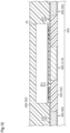
- FIG. 1 is a schematic plan view showing an encapsulation resin and interconnects in a first embodiment of a semiconductor device.
- FIG. 2 is a schematic cross-sectional view of the semiconductor device taken along line F 2 -F 2 in FIG. 1 .
- FIG. 3 is an enlarged partial view of FIG. 2 .
- FIG. 4 is a schematic back view of the semiconductor device.
- FIG. 5 is a schematic plan view showing the positional relationship of a pillar and an interconnect.
- FIG. 6 is a schematic diagram showing an example of a step of manufacturing the semiconductor device of the first embodiment.
- FIG. 7 is a schematic diagram showing an example of a step of manufacturing the semiconductor device following the step shown in FIG. 6 .
- FIG. 8 is a schematic diagram showing an example of a step of manufacturing the semiconductor device following the step shown in FIG. 7 .
- FIG. 9 is a schematic diagram showing an example of a step of manufacturing the semiconductor device following the step shown in FIG. 8 .
- FIG. 10 is a schematic diagram showing an example of a step of manufacturing the semiconductor device following the step shown in FIG. 9 .
- FIG. 11 is a schematic diagram showing an example of a step of manufacturing the semiconductor device following the step shown in FIG. 10 .
- FIG. 12 is a schematic diagram showing an example of a step of manufacturing the semiconductor device following the step shown in FIG. 11 .
- FIG. 13 is a schematic diagram showing an example of a step of manufacturing the semiconductor device following the step shown in FIG. 12 .
- FIG. 14 is a schematic back view showing the positional relationship of an encapsulation resin and bonding layer pieces in a second embodiment of a semiconductor device.
- FIG. 15 is a schematic cross-sectional view showing a cross-sectional structure of a portion of the semiconductor device taken along line F 15 -F 15 in FIG. 14 .
- FIG. 16 is a schematic cross-sectional view showing a cross-sectional structure of the semiconductor device taken along line F 16 -F 16 in FIG. 14 .
- FIG. 17 is a back view showing a third embodiment of a semiconductor device.
- FIG. 18 is a back view showing a modified example of a semiconductor device.
- FIG. 1 for the sake of convenience, a semiconductor element 20 and bonding layer pieces 70 , which will be described later, are indicated by double-dashed lines. Also, for the sake of convenience, FIG. 1 does not show a portion of an encapsulation resin 40 , which will be described later.
- FIG. 3 is an enlarged view of one of the bonding layer pieces 70 shown in FIG. 2 and its surroundings.
- a pillar 110 is transparently shown and indicated by a solid line to show the positional relationship of the pillar 110 and an interconnect 30 , which will be described later.
- FIGS. 4 and 5 do not show a conductive film 120 , which will be described later.
- the semiconductor device 10 includes a semiconductor element 20 , interconnects 30 electrically connected to the semiconductor element 20 , and an encapsulation resin 40 encapsulating the semiconductor element 20 and the interconnects 30 .
- the semiconductor device 10 is configured to be surface-mounted on a circuit board (not shown) of various electronic apparatuses.
- the semiconductor device 10 has a package structure of a surface mount type.
- the encapsulation resin 40 defines an outer surface of the semiconductor device 10 .
- the encapsulation resin 40 is rectangular and flat.
- the semiconductor device 10 is rectangular and flat.
- the thickness-wise direction of the encapsulation resin 40 is referred to as a z-direction.
- a direction along one side of the semiconductor device 10 orthogonal to the z-direction is referred to as an x-direction
- a direction orthogonal to the x-direction and the z-direction is referred to as a y-direction.
- the y-direction also extends along one side of the semiconductor device 10 .
- the encapsulation resin 40 is square as viewed in the z-direction.
- the semiconductor device 10 is square as viewed in the z-direction.
- the shape of the encapsulation resin 40 (the shape of the semiconductor device 10 ) may be changed in any manner.
- the encapsulation resin 40 (semiconductor device 10 ) may be rectangular such that the sides in the x-direction are longer than the sides in the y-direction or the sides in the y-direction are longer than the sides in the x-direction.
- the encapsulation resin 40 includes a resin front surface 41 and a resin back surface 42 opposite to the resin front surface 41 .
- the encapsulation resin 40 further includes four resin side surfaces joining the resin front surface 41 and the resin back surface 42 in the z-direction, namely, a first resin side surface 43 , a second resin side surface 44 , a third resin side surface 45 , and a fourth resin side surface 46 (refer to FIG. 1 ).
- the encapsulation resin 40 includes a flat substrate part 50 and an encapsulation part 60 formed on the substrate part 50 .
- the substrate part 50 is a support member used as a base of the semiconductor device 10 .
- the semiconductor element 20 is mounted on the substrate part 50 .
- the substrate part 50 is formed from an insulative material.
- the substrate part 50 is formed from, for example, a black epoxy resin.
- the material forming the substrate part 50 may be any insulative material.
- the substrate part 50 forms a portion of the encapsulation resin 40 located toward the resin back surface 42 .
- the substrate part 50 includes a substrate front surface 51 facing in the same direction as the resin front surface 41 and a substrate back surface 52 defining the resin back surface 42 .
- the substrate part 50 includes substrate side surfaces defining a portion of the first to fourth resin side surfaces 43 to 46 .
- the encapsulation part 60 is an encapsulation member that encapsulates the semiconductor element 20 .
- the encapsulation part 60 is formed from an insulative material.
- the encapsulation part 60 is formed from, for example, a black epoxy resin.
- the material forming the encapsulation part 60 may be any insulative material.
- the substrate part 50 and the encapsulation part 60 may be formed from a material including, for example, a filler that improves heat dissipation properties.
- each of the substrate part 50 and the encapsulation part 60 is formed from a black epoxy resin.
- the ratio of a filler contained in the epoxy resin differs between the substrate part 50 and the encapsulation part 60 .
- an interface is formed in the boundary between the substrate part 50 and the encapsulation part 60 .
- the encapsulation part 60 forms a portion of the encapsulation resin 40 located toward the resin front surface 41 .
- the encapsulation part 60 includes an encapsulation front surface 61 defining the resin front surface 41 and an encapsulation back surface 62 opposite to the encapsulation front surface 61 .
- the encapsulation back surface 62 is in contact with the substrate front surface 51 of the substrate part 50 .
- the encapsulation back surface 62 of the encapsulation part 60 and the substrate front surface 51 of the substrate part 50 form the interface between the substrate part 50 and the encapsulation part 60 .
- the encapsulation part 60 includes resin side surfaces defining a portion of the first to fourth resin side surfaces 43 to 46 .
- the substrate part 50 is thinner than the encapsulation part 60 .
- the substrate part 50 is thinner than the semiconductor element 20 .
- the substrate part 50 has a thickness of 40 ⁇ m or greater and 70 ⁇ m or less.
- the thickness of the substrate part 50 is defined by the dimension between the substrate front surface 51 and the substrate back surface 52 in the z-direction.
- the thickness of the encapsulation part 60 is defined by the dimension between the encapsulation front surface 61 and the encapsulation back surface 62 in the z-direction.
- the thickness of the semiconductor element 20 is defined by the dimension between an element front surface 21 and an element back surface 22 in the z-direction.
- the semiconductor element 20 encapsulated in the encapsulation part 60 is, for example, an integrated circuit (IC) such as a large scale integration (LSI).
- the semiconductor element 20 may be a voltage-controlling element such as a low dropout (LDO) regulator, an amplifying element such as an operational amplifier, or a discrete semiconductor element such as a diode or various sensors.
- LDO low dropout
- an amplifying element such as an operational amplifier
- a discrete semiconductor element such as a diode or various sensors.
- the semiconductor element 20 is flat.
- the semiconductor element 20 is square as viewed in the z-direction.
- the shape of the semiconductor element 20 as viewed in the z-direction may be changed in any manner.
- the semiconductor element 20 may be rectangular such that the sides in the x-direction are longer than the sides in the y-direction or the sides in the y-direction are longer than the sides in the x-direction.
- the semiconductor element 20 includes an element front surface 21 and an element back surface 22 opposite to the element front surface 21 .
- the element front surface 21 faces in the same direction as the resin front surface 41 .
- the resin front surface 41 faces in the same direction as the element front surface 21 .
- the element back surface 22 faces in the same direction as the resin back surface 42 .
- the element back surface 22 is opposed to the substrate front surface 51 of the substrate part 50 .
- the semiconductor element 20 further includes four element side surfaces joining the element front surface 21 and the element back surface 22 in the z-direction.
- the semiconductor element 20 is entirely covered by the encapsulation resin 40 (encapsulation part 60 ).
- the interconnects 30 are arranged. As shown in FIG. 2 , the interconnects 30 are formed on the substrate part 50 . More specifically, the interconnects 30 are formed on the substrate front surface 51 of the substrate part 50 . Since the substrate front surface 51 of the substrate part 50 is a flat surface orthogonal to the z-direction, the interconnects 30 extend in a direction orthogonal to the z-direction.
- the interconnects 30 are opposed to the element back surface 22 of the semiconductor element 20 . As viewed in the z-direction, each interconnect 30 extends from a position opposed to the element back surface 22 of the semiconductor element 20 to the outside of the semiconductor element 20 . In other words, the interconnect 30 includes an extension extending out from the semiconductor element 20 as viewed in the z-direction.
- the interconnect 30 includes a metal layer and a main interconnect layer.
- the metal layer is formed as a seed layer for forming the main interconnect layer.
- the metal layer is formed from a material including, for example, titanium (Ti).
- the metal layer includes a Ti layer and a copper (Cu) layer in contact with the Ti layer.
- the metal layer is formed on the substrate front surface 51 of the substrate part 50 . More specifically, the Ti layer is formed on the substrate front surface 51 .
- the Cu layer is formed on the Ti layer. Thus, the metal layer is formed on the substrate front surface 51 .
- the main interconnect layer is formed on the metal layer. More specifically, the main interconnect layer is formed on the Cu layer of the metal layer. Thus, each interconnect 30 has a stacking structure of the metal layer and the main interconnect layer.
- the main interconnect layer is formed from, for example, Cu or an alloy including Cu.
- each interconnect 30 extends toward one of the first to fourth resin side surfaces 43 to 46 from a position where the interconnect 30 overlaps the semiconductor element 20 .
- Each interconnect 30 is exposed from the resin side surface corresponding to the interconnect 30 .
- each interconnect 30 includes an exposed interconnect side surface 31 exposed from the resin side surface corresponding to the interconnect 30 .
- the exposed interconnect side surface 31 is flush with the resin side surface.
- the resin side surface corresponding to the interconnect 30 refers to the resin side surface that is located closest to the interconnect 30 .
- the resin side surface corresponding to the interconnect 30 also refers to the resin side surface on which the exposed interconnect side surface 31 of the interconnect 30 is formed.
- FIG. 3 is a diagram showing an example of the structure connecting the semiconductor element 20 and the interconnect 30 .
- the semiconductor element 20 includes an element substrate 23 , connection terminals 24 , an insulation film 25 , and a connection wiring line 26 .
- the connection wiring line 26 and the insulation film 25 are arranged on the element substrate 23 .
- the element substrate 23 is a semiconductor substrate and is formed from a material including, for example, silicon (Si).
- the element substrate 23 is a Si substrate.
- the element substrate 23 includes a front surface 23 A and a back surface 23 B.
- the front surface 23 A of the element substrate 23 faces the same direction as the element front surface 21 of the semiconductor element 20 .
- the back surface 23 B faces in the same direction as the element back surface 22 of the semiconductor element 20 .
- the front surface 23 A of the element substrate 23 defines the element front surface 21 of the semiconductor element 20 .
- the back surface 23 B refers to a surface including a functional element (e.g., transistor) of the semiconductor element 20 .
- each connection terminal 24 is located toward the interconnect 30 from the back surface 23 B of the element substrate 23 .
- the connection terminal 24 includes a conductor 24 A and a barrier layer 24 B.
- the conductor 24 A is formed from a material including, for example, Cu.
- the conductor 24 A forms a portion of the connection terminal 24 located toward the element substrate 23 .
- the barrier layer 24 B includes, for example, a Ni layer.
- the barrier layer 24 B is formed on the conductor 24 A to cover a distal surface of the conductor 24 A.
- the barrier layer 24 B limits interfusion of the conductor 24 A into the bonding layer piece 70 , which will be described later.
- the structure of the barrier layer 24 B may be changed in any manner.
- the barrier layer 24 B may be formed by stacking a Ni layer, a Pd layer, and a Au layer.
- the connection terminal 24 is cylindrical-rod-shaped. Thus, as viewed in the z-direction, the connection terminal 24 is circular.
- the insulation film 25 covers the back surface 23 B of the element substrate 23 and exposes the connection terminals 24 .
- the connection wiring line 26 is arranged on the insulation film 25 to connect the element substrate 23 to the connection terminal 24 . More specifically, the insulation film 25 includes an opening 25 A that exposes the back surface 23 B of the element substrate 23 .
- the connection wiring line 26 is arranged in the opening 25 A and extends outward from the opening 25 A.
- the connection terminal 24 is arranged on the portion of the connection wiring line 26 extending outward from the opening 25 A. Thus, the connection terminal 24 and the opening 25 A of the insulation film 25 are arranged at different positions.
- the connection wiring line 26 electrically connects the element substrate 23 to the connection terminal 24 . As shown in FIG. 1 , in the z-direction, the interconnects 30 are opposed to the connection terminals 24 .
- the insulation film 25 is formed from a material including, for example, a polyimide resin.
- the material forming the insulation film 25 may be changed in any manner.
- the insulation film 25 may be formed from a material including a silicon nitride (SiN).
- the semiconductor element 20 is connected to the interconnects 30 by the conductive bonding layer pieces 70 .
- the bonding layer pieces 70 are arranged between the semiconductor element 20 and the interconnects 30 .
- the bonding layer pieces 70 electrically connect the semiconductor element 20 to the interconnects 30 .
- the bonding layer pieces 70 are configured to bond the connection terminals 24 of the semiconductor element 20 to the interconnects 30 .
- the bonding layer pieces 70 include a solder layer.
- the bonding layer pieces 70 are formed of tin (Sn) or an alloy including Sn.
- the alloy including Sn includes, for example, a tin-silver (Ag)-based alloy and a tin-antimony (Sb)-based alloy.
- the bonding layer piece 70 is in contact with the barrier layer 24 B of the connection terminal 24 of the semiconductor element 20 . Thus, the bonding layer piece 70 is bonded to the connection terminal 24 .
- multiple bonding layer pieces 70 may be arranged on a single interconnect 30 or a single bonding layer piece 70 may be arranged on the interconnect 30 .
- the relationship of the interconnect 30 with the number of bonding layer pieces 70 is set, for example, based on the amount of current flowing through the interconnect 30 .
- a protective layer 80 is arranged between the bonding layer piece 70 and the interconnect 30 . That is, the semiconductor device 10 includes the protective layer 80 arranged between the interconnect 30 and the bonding layer piece 70 .
- the protective layer 80 is formed from a material including Ni.
- the protective layer 80 is formed on the interconnect 30 .
- the protective layer 80 is formed on a portion of the interconnect 30 opposed to the connection terminal 24 of the semiconductor element 20 in the z-direction.
- the thickness of the protective layer 80 (dimension of the protective layer 80 in the z-direction) is, for example, greater than or equal to 3 ⁇ m and less than or equal to 5 ⁇ m.
- the protective layer 80 is circular as viewed in the z-direction.
- the protective layer 80 is greater in diameter than the connection terminal 24 .
- the bonding layer piece 70 is formed on the protective layer 80 .
- the bonding layer piece 70 is greater in thickness than the protective layer 80 .
- the connection terminal 24 of the semiconductor element 20 is electrically connected to the interconnect 30 by the bonding layer piece 70 and the protective layer 80 .
- the semiconductor element 20 is mounted on the interconnects 30 .
- the bonding layer piece 70 is circular as viewed in the z-direction. As shown in FIG. 3 , since the protective layer 80 is greater in diameter than the connection terminal 24 , the bonding layer piece 70 is truncated-cone-shaped.
- the semiconductor device 10 includes external connection terminals 90 electrically connected to the semiconductor element 20 by the interconnects 30 (refer to FIG. 1 ).
- the external connection terminals 90 are arranged on an outermost peripheral portion of the resin back surface 42 .
- the external connection terminals 90 are located outward from the semiconductor element 20 .
- the external connection terminals 90 are formed from, for example, Cu or an alloy including Cu.
- the external connection terminals 90 are formed by, for example, electrolytic plating.
- the external connection terminals 90 are arranged adjacent to the first to fourth resin side surfaces 43 to 46 as viewed in the z-direction. More specifically, multiple external connection terminals 90 are arranged adjacent to the first resin side surface 43 . The external connection terminals 90 are separated from each other in a direction extending along the first resin side surface 43 as viewed in the z-direction. Multiple external connection terminals 90 are arranged adjacent to the second resin side surface 44 . The external connection terminals 90 are separated from each other in a direction extending along the second resin side surface 44 as viewed in the z-direction. Multiple external connection terminals 90 are arranged adjacent to the third resin side surface 45 .
- the external connection terminals 90 are separated from each other in a direction extending along the third resin side surface 45 as viewed in the z-direction. Multiple external connection terminals 90 are arranged adjacent to the fourth resin side surface 46 . The external connection terminals 90 are separated from each other in a direction extending along the fourth resin side surface 46 as viewed in the z-direction. As shown in FIG. 4 , the external connection terminals 90 are arranged outward from the semiconductor element 20 as viewed in the z-direction. As described above, the semiconductor device 10 of the present embodiment is of a fan-out type in which the external connection terminals 90 are located outward from the semiconductor element 20 .
- the external connection terminal 90 is rectangular and includes long sides and short sides.
- the short sides of the external connection terminal 90 extend in an arrangement direction of the external connection terminals 90 .
- the long sides extend in a direction orthogonal to the arrangement direction as viewed in the z-direction.
- the external connection terminals 90 are exposed from the resin back surface 42 and one of the first to fourth resin side surfaces 43 to 46 . More specifically, as viewed in the z-direction, the external connection terminals 90 located adjacent to the first resin side surface 43 are exposed from the resin back surface 42 and the first resin side surface 43 . As viewed in the z-direction, the external connection terminals 90 located adjacent to the second resin side surface 44 are exposed from the resin back surface 42 and the second resin side surface 44 . As viewed in the z-direction, the external connection terminals 90 located adjacent to the third resin side surface 45 are exposed from the resin back surface 42 and the third resin side surface 45 . As viewed in the z-direction, the external connection terminals 90 located adjacent to the fourth resin side surface 46 are exposed from the resin back surface 42 and the fourth resin side surface 46 .
- the external connection terminals 90 are connected to the interconnects 30 .
- the external connection terminals 90 are arranged on the substrate part 50 and extend from the interconnects 30 toward the resin back surface 42 .
- the external connection terminals 90 extend through the substrate part 50 in the z-direction.
- the external connection terminals 90 are covered by the interconnects 30 in the z-direction and thus do not project from the substrate front surface 51 of the substrate part 50 toward the resin front surface 41 .
- the external connection terminals 90 do not project from the substrate back surface 52 (resin back surface 42 ) of the substrate part 50 in a direction opposite to the substrate front surface 51 .
- a thickness T of the external connection terminal 90 is equal to a thickness TB of the substrate part 50 .
- the resin back surface 42 includes four corners, each of which includes a corner terminal 100 .
- the corner terminal 100 and the external connection terminal 90 are formed from the same material.
- the corner terminal 100 is exposed from the resin back surface 42 and two resin side surfaces forming the corner.
- the corner terminal 100 is electrically disconnected from the interconnects 30 .
- the corner terminal 100 extends through the substrate part 50 in the z-direction.
- the corner terminal 100 has a thickness that is equal to the thickness T of the external connection terminal 90 .
- a corner interconnect 101 is arranged on the substrate front surface 51 of the substrate part 50 to overlap the corner terminal 100 (refer to FIG. 4 ).
- the corner interconnect 101 which differs from the interconnect 30 , is electrically disconnected from the semiconductor element 20 .
- the corner interconnect 101 and the interconnect 30 are formed from, for example, the same material.
- the corner interconnect 101 may have a stacking structure of a metal layer and a main interconnect layer.
- the semiconductor device 10 includes a pillar 110 exposed from the resin back surface 42 .
- the pillar 110 is arranged to overlap the semiconductor element 20 .
- the pillar 110 is arranged in the center of the resin back surface 42 .
- the pillar 110 and the external connection terminals 90 are formed from the same material.
- the pillar 110 is a thermal pad that releases heat from the semiconductor element 20 to the outside of the encapsulation resin 40 .
- the pillar 110 extends through the substrate part 50 .
- the pillar 110 is covered by the interconnect 30 in the z-direction and thus does not project from the substrate front surface 51 of the substrate part 50 toward the resin front surface 41 .
- the pillar 110 does not project from the substrate back surface 52 (resin back surface 42 ) of the substrate part 50 in a direction opposite to the substrate front surface 51 .
- the pillar 110 has a thickness TP that is equal to the thickness TB of the substrate part 50 .
- the thickness TP of the pillar 110 is equal to the thickness T of the external connection terminal 90 .
- the interconnects 30 include an interconnect 32 extending from the second resin side surface 44 to the center of the resin back surface 42 .
- the pillar 110 is connected to the interconnect 32 .
- the pillar 110 is electrically connected to the interconnect 32 .
- the interconnect 32 is wider than the other interconnects 30 .
- the interconnect 32 may be divided into an outer part 32 A located toward the second resin side surface 44 , an inner part 32 B located toward the center of the substrate front surface 51 , and a joining part 32 C that joins the outer part 32 A and the inner part 32 B.
- the outer part 32 A extends from the second resin side surface 44 toward the center of the substrate front surface 51 in the x-direction. As viewed in the z-direction, the outer part 32 A may be divided into a first section overlapping the semiconductor element 20 and a second section extending from the first section beyond the semiconductor element 20 . The second section is connected to two external connection terminals 90 .
- the outer part 32 A is equal in width-wise dimension to interconnects 33 and 34 , which are located adjacent to the outer part 32 A in the y-direction.
- the interconnects 33 and 34 are greater in width-wise dimension than the interconnects 30 excluding the interconnects 32 to 34 .
- Each of the interconnects 32 to 34 is connected to two of the external connection terminals 90 .
- a greater number of bonding layer pieces 70 is arranged on each of the interconnects 32 to 34 than on the other interconnects 30 .
- the interconnects 30 excluding the interconnects 32 to 34 are each connected to one external connection terminal 90 .
- the inner part 32 B is greater in width-wise dimension than the outer part 32 A. As viewed in the x-direction, the inner part 32 B partially overlaps the interconnects 33 and 34 . Among four corners of the inner part 32 B, the corner located toward the first resin side surface 43 and the third resin side surface 45 includes a chamfered slope 32 BA.
- the joining part 32 C is arranged between the outer part 32 A and the inner part 32 B in the x-direction.
- the joining part 32 C is tapered so that the width increases from the outer part 32 A toward the inner part 32 B.
- the pillar 110 overlaps the inner part 32 B.
- the pillar 110 is connected to the inner part 32 B.
- the pillar 110 has a width-wise dimension WP that is slightly smaller than a width-wise dimension W of the inner part 32 B.
- the pillar 110 has a length LP in the x-direction that is equal to a length L of the inner part 32 B in the x-direction.
- the width-wise dimension WP of the pillar 110 is larger than the width-wise dimension of the outer part 32 A (refer to FIG. 1 ).
- the width-wise dimension WP of the pillar 110 (refer to FIG.
- the width-wise dimension WP of the pillar 110 is larger than the long side of the external connection terminal 90 .
- the length LP (refer to FIG. 5 ) of the pillar 110 is greater than the long side of the external connection terminal 90 .
- the bonding layer pieces 70 are arranged on the outer part 32 A, whereas the pillar 110 is arranged on the inner part 32 B.
- the bonding layer pieces 70 and the pillar 110 each of which overlaps with the interconnect 32 in the z-direction, do not overlap with each other in the z-direction.
- the bonding layer pieces 70 are arranged between the pillar 110 and the external connection terminals 90 connected to the interconnect 32 in the x-direction.
- the pillar 110 is quadrilateral (rectangular).
- the pillar 110 includes a curved portion 111 that relieves stress from the encapsulation resin 40 .
- the curved portion 111 is formed on at least a part of the portion of the pillar 110 contacting the encapsulation resin 40 .
- the curved portion 111 is arranged on three of the four corners of the pillar 110 .
- the pillar 110 is shaped as a polygon including corners that are rounded as the curved portions 111 as viewed in the z-direction.
- the pillar 110 is shaped as a quadrilateral including three corners that are rounded as the curved portions 111 as viewed in the z-direction.
- the curved portion 111 is arc-shaped.
- the curved portion 111 is quadrantal.
- the radius of the curved portion 111 is, for example, greater than or equal to the largest diameter of the bonding layer pieces 70 (refer to FIG. 1 ).
- the curved portion 111 is convex toward the encapsulation resin 40 as viewed in the z-direction.
- each curved portion 111 is arranged to overlap the interconnect 32 (inner part 32 B).
- the interconnect 32 includes a portion overlapping the curved portion 111 as viewed in the z-direction.
- the interconnect 32 (inner part 32 B) includes a portion extending out from the curved portion 111 .
- the corner that does not include the curved portion 111 includes a chamfered slope 112 .
- the slope 112 is arranged on one of the four corners of the pillar 110 that is located toward the first resin side surface 43 and the third resin side surface 45 .
- the slope 112 is arranged at a position corresponding to the slope 32 BA of the interconnect 32 .
- the conductive films 120 are arranged on portions of the external connection terminals 90 exposed from the encapsulation resin 40 .
- the conductive films 120 cover the exposed interconnect side surfaces 31 of the interconnects 30 in addition to the external connection terminals 90 .
- a conductive film 120 is arranged on a portion of the pillar 110 exposed from the resin back surface 42 .
- the conductive films 120 are formed by, for example, electroless plating. Further, although not shown in the drawings, a conductive film 120 is arranged on a portion of the corner terminal 100 exposed from the encapsulation resin 40 .
- metal pillars 900 are formed on a semiconductor wafer 800 that is formed from a monocrystalline Si material.
- the metal pillars 900 include the external connection terminals 90 , the corner terminals 100 (refer to FIG. 4 ), and the pillar 110 . That is, the external connection terminals 90 , the corner terminals 100 , and the pillar 110 are formed simultaneously.
- the metal pillars 900 are greater in thickness than the external connection terminals 90 , the corner terminals 100 , and the pillar 110 .
- the metal pillars 900 are formed by, for example, electrolytic plating. More specifically, a seed layer 901 is formed on the semiconductor wafer 800 . Then, the seed layer 901 undergoes photolithography to form a mask (not shown). The mask is removed after a plating metal 902 is formed in contact with the seed layer 901 . Thus, each metal pillar 900 has a stacking structure of the seed layer 901 and the plating metal 902 .
- the seed layer 901 is formed on the semiconductor wafer 800 by, for example, sputtering. Next, for example, the seed layer 901 is covered by a photosensitive resist layer, and the resist layer undergoes reaction with light and development to form a mask having openings. Electrolytic plating in which the seed layer 901 is used as a conductive path is performed so that plating metal 902 deposits on the surface of the seed layer 901 exposed from the mask. The steps described above form the metal pillars 900 . Subsequent to formation of the metal pillars 900 , the mask is removed.
- a substrate layer 850 is formed on the semiconductor wafer 800 .
- the substrate layer 850 is a resin layer that forms the substrate part 50 of the semiconductor device 10 and encapsulates the metal pillars 900 between the substrate layer 850 and the semiconductor wafer 800 .
- the substrate layer 850 is formed from, for example, a black epoxy resin.
- the substrate layer 850 shown in FIG. 7 is greater in thickness than the substrate part 50 .
- the substrate layer 850 and the metal pillars 900 are ground.
- the substrate layer 850 and the metal pillars 900 are ground from the side opposite to the semiconductor wafer 800 .
- the metal pillars 900 are exposed from the substrate layer 850 .
- it is preferred that the thickness of the substrate layer 850 is less than or equal to 90 ⁇ m.
- an interconnect layer 830 is formed.
- the interconnect layer 830 is a metal layer that forms the interconnects 30 and the corner interconnects 101 (refer to FIG. 1 ) of the semiconductor device 10 and is formed on a surface 851 of the substrate layer 850 and the metal pillars 900 that have been ground.
- the surface 851 of the substrate layer 850 defines the substrate front surface 51 of the substrate part 50 .
- the interconnect layer 830 includes a metal layer and a main interconnect layer.
- the metal layer is formed by, for example, sputtering on the surface 851 of the substrate layer 850 and a portion of the metal pillars 900 that have been ground.
- the metal layer includes, for example, a Ti layer and a Cu layer.
- the Ti layer is formed on the surface 851 of the substrate layer 850 and a portion of the metal pillars 900 .
- the Cu layer is formed in contact with the Ti layer.
- the metal layer undergoes photolithography to form a mask.
- the metal layer is covered by a photosensitive resist layer, and the resist layer undergoes exposure and development to form a mask having openings.
- the openings in the mask correspond to positions where the interconnects 30 and the corner interconnects 101 (refer to FIG. 4 ) are formed.
- the main interconnect layer is formed by electrolytic plating in which the metal layer is used as a conductive path so that plating metal deposits on the surface of the metal layer exposed from the openings of the mask. Subsequently, the mask is removed.
- the portion of the metal layer that does not overlap the main interconnect layer is removed.
- the main interconnect layer and the metal layer undergo photolithography to form a mask.
- openings are formed in the portion of the metal layer that does not overlap the main interconnect layer.
- the metal layer exposed from the openings of the mask is removed.
- the mask is removed. The steps described above form the interconnect layer 830 , which forms the interconnects 30 and the corner interconnects 101 .
- the substrate layer 850 and the metal pillars 900 are reduced in thickness prior to formation of the interconnect layer 830 , warpage of the semiconductor wafer 800 is limited after formation of the interconnect layer 830 . Thus, the semiconductor wafer 800 is readily transported in a step subsequent to formation of the interconnect layer 830 .
- a protective layer 880 and a bonding layer 870 are formed.
- the protective layer 880 is formed by, for example, electrolytic plating in which the interconnect layer 830 is used as a conductive path.
- the protective layer 880 is formed from, for example, Ni. As viewed in the thickness-wise direction of the substrate layer 850 , the protective layer 880 is circular.
- FIG. 10 shows a state of the bonding layer 870 that has undergone the reflow process. As viewed in the thickness-wise direction of the substrate layer 850 , the bonding layer 870 is circular.
- the semiconductor element 20 is mounted on the interconnect layer 830 .
- the semiconductor element 20 is mounted by flip chip bonding (FCB).
- solder layer is formed from, for example, the same material as that forming the bonding layer 870 (refer to FIG. 10 ).
- the reflow process is performed to smooth the surface of the solder layer of the semiconductor element 20 .
- the solder layer is circular.
- a flux is applied to the solder layer of the semiconductor element 20 , and then the semiconductor element 20 is mounted on the bonding layer 870 using, for example, a flip-chip bonder.
- the semiconductor element 20 is temporarily attached to the bonding layer 870 .
- the reflow process is performed so that the bonding layer 870 and the solder layer of the semiconductor element 20 change the phase to a liquid state, and then the bonding layer 870 and the solder layer of the semiconductor element 20 are cooled and solidified.
- the semiconductor element 20 is bonded to the bonding layer 870 .
- the bonding layer piece 70 (refer to FIG. 3 ) is formed of the bonding layer 870 and the solder layer of the semiconductor element 20 .
- the bonding layer piece 70 is truncated-cone-shaped.
- an encapsulation layer 860 that encapsulates the semiconductor element 20 is formed.
- the encapsulation layer 860 forms the encapsulation part 60 (refer to FIG. 2 ) of the encapsulation resin 40 .
- the encapsulation layer 860 is formed from, for example, a black epoxy resin.
- the encapsulation resin 40 is formed of the substrate layer 850 and the encapsulation layer 860 .
- the encapsulation layer 860 is formed by, for example, compression molding.
- the semiconductor wafer 800 (refer to FIG. 12 ) is removed.
- the upper and lower sides in FIG. 12 are reversed in FIG. 13 .
- the semiconductor wafer 800 is removed from the substrate layer 850 by, for example, grinding.
- the substrate layer 850 and the metal pillars 900 are partially removed in the thickness-wise direction of the substrate layer 850 .
- the seed layer 901 (refer to FIG. 6 ) is removed from the metal pillars 900 .
- the metal pillars 900 are exposed from the substrate layer 850 at the side opposite from the encapsulation layer 860 .
- the substrate layer 850 includes a back surface 852 defining the substrate back surface 52 of the substrate part 50 .
- the thickness of the substrate layer 850 becomes equal to the thickness of the substrate part 50 .
- the thickness of the metal pillars 900 becomes equal to the thickness of each of the external connection terminals 90 , the corner terminals 100 (refer to FIG. 4 ), and the pillar 110 .
- the thickness of the substrate layer 850 is greater than or equal to 40 ⁇ m and less than or equal to 70 ⁇ m.
- the means of removing the semiconductor wafer 800 may be changed in any manner.
- a separation film may be formed in advance, and the semiconductor wafer 800 may be removed by separation.
- the substrate layer 850 and the metal pillars 900 may be ground.
- a step of cutting the substrate layer 850 and the encapsulation layer 860 for singulation and a step of forming a conductive film are performed.
- the substrate layer 850 and the encapsulation layer 860 are cut, the side surface of the metal pillar 900 is exposed from the substrate layer 850 , and the side surface of the interconnect layer 830 is exposed from the encapsulation layer 860 .
- the conductive film is formed on the surface of the metal pillar 900 and the side surface of the interconnect layer 830 exposed from the substrate layer 850 and the encapsulation layer 860 .
- the conductive film is formed by, for example, electroless plating. The steps described above manufacture the semiconductor device 10 .
- Changes in the temperature of the semiconductor device 10 produce stress is in the substrate part 50 due to the difference between the thermal expansion coefficient of the substrate part 50 and the thermal expansion coefficient of the pillar 110 and the external connection terminals 90 .
- the pillar 110 having a greater volume than the external connection terminal 90 , expands and contracts by a greater amount than the external connection terminal 90 .
- cracks are likely to be formed in the substrate part 50 located adjacent to the pillar 110 .
- the inventor of this application found from test results and the like that when the pillar 110 includes a non-chamfered corner, stress is increased in the substrate part 50 located adjacent to the pillar 110 . As a result, cracks are more likely to be formed in the substrate part 50 .
- Cracks are formed in the substrate part 50 from the substrate back surface 52 toward the substrate front surface 51 . That is, the cracks extend in the thickness-wise direction of the substrate part 50 . If the cracks extend to the interconnects 30 , the interconnects 30 may contact an object (e.g., moisture) present outside the semiconductor device 10 .
- an object e.g., moisture
- the thickness of the substrate part 50 may be increased to hinder the cracks from extending to the interconnects 30 . This improves the strength of the substrate part 50 . Thus, cracks are less likely to be formed.
- the substrate layer 850 and the metal pillars 900 are cut to decrease the thickness of the substrate layer 850 and the thickness of the metal pillars 900 .
- the substrate layer 850 is partially cut to ensure that the metal pillars 900 are exposed from the substrate layer 850 .
- the thickness of the substrate layer 850 that has been cut is equal to the thickness of the substrate part 50 of the semiconductor device 10 .
- the metal pillars 900 form the pillar 110 and the external connection terminals 90 .
- the thickness of the substrate part 50 is decreased, the strength of the substrate part 50 is decreased. As a result, cracks are likely to be formed due to stress produced in the substrate part 50 .
- the curved portions 111 are arranged in the corners of the pillar 110 .
- stress applied to the substrate part 50 adjacent to the pillar 110 is decreased.
- cracks are less likely to be formed in the substrate part 50 .
- the bonding layer piece 70 is arranged so that the bonding layer piece 70 is circular as viewed in the z-direction.
- stress applied to the bonding layer piece 70 is decreased.
- cracks are less likely to be formed in the bonding layer piece 70 .
- the semiconductor device 10 of the present embodiment has the following advantages.
- the curved portions 111 relieve stress applied from the encapsulation resin 40 to the pillar 110 . Accordingly, stress (reaction force) applied from the pillar 110 to the encapsulation resin 40 is decreased. Thus, even when the temperature of the semiconductor device 10 is changed, cracks caused by the pillar 110 are less likely to be formed in the encapsulation resin 40 .
- stress is likely to be produced in the encapsulation resin 40 located adjacent to a corner of the pillar 110 .
- the corners of the pillar 110 are rounded to decrease the stress applied from the pillar 110 to the encapsulation resin 40 .
- the pillar 110 includes the curved portions 111 so that stress applied from the pillar 110 to the encapsulation resin 40 is decreased. Therefore, even when the encapsulation resin 40 includes a portion surrounded by the interconnect 32 and the pillar 110 , cracks are less likely to be formed in the encapsulation resin 40 .
- heat is released from the semiconductor element 20 to the outside of the semiconductor device 10 through the pillar 110 .
- the solder adheres to a portion of each external connection terminal 90 exposed from one of the first to fourth resin side surfaces 43 to 46 .
- the mount state of the semiconductor device 10 on the circuit board with the solder is visually recognized. This facilitates the checking of the mount state of the semiconductor device 10 on the circuit board.
- the pillar 110 is bonded to the circuit board by the conductive film 120 .
- heat is readily transferred from the semiconductor element 20 to the circuit board through the pillar 110 and the conductive film 120 .
- the shape of the bonding layer piece 70 arranged on the protective layer 80 tends to be dependent on the shape of the protective layer 80 .
- the bonding layer piece 70 is readily shaped as a circle by shaping the protective layer 80 as a circle.
- the pillar 110 is arranged in the substrate part 50 , having the smaller thickness.
- the corners of the pillar 110 include the curved portions 111 so that stress applied from the pillar 110 to the substrate part 50 is decreased. As a result, cracks are less likely to be formed in the substrate part 50 .
- FIGS. 14 and 16 A second embodiment of a semiconductor device 10 will now be described with reference to FIGS. 14 and 16 .
- the present embodiment mainly differs from the first embodiment in the structure of the external connection terminal 90 .
- same reference numerals are given to those components that are the same as the corresponding components of the semiconductor device 10 in the first embodiment. Such components will not be described in detail.
- FIG. 14 does not show the conductive film 120 .
- FIG. 14 schematically shows interconnects 35 connected to pillars 130 and does not show the remaining interconnects 30 .
- FIG. 14 is a back view showing the present embodiment of a semiconductor device 10 .
- the external connection terminals 90 are arranged on an outermost peripheral portion of the encapsulation resin 40 as viewed in the z-direction.
- the external connection terminals 90 include two types of external connection terminal, namely, external connection terminals 90 A and external connection terminals 90 B.
- the external connection terminals 90 A have the same structure as the external connection terminals 90 of the first embodiment.
- the external connection terminals 90 B are formed of the pillars 130 .
- the semiconductor device 10 includes four pillars 130 . Therefore, four external connection terminals 90 B are arranged.
- the external connection terminals 90 include terminals formed of the pillars 130 .
- the pillars 130 are thermal pads that release heat from the semiconductor element 20 to the outside of the encapsulation resin 40 .
- the pillars 130 extend in the y-direction. In the present embodiment, the y-direction corresponds to an “extension direction of pillar.”
- the pillars 130 may extend in the x-direction.
- the multiple (four) pillars 130 include two first pillars 130 A and two second pillars 130 B.
- the first pillars 130 A extend from the fourth resin side surface 46 toward the third resin side surface 45 .
- the second pillars 130 B extend from the third resin side surface 45 toward the fourth resin side surface 46 .
- the fourth resin side surface 46 corresponds to a “first end in first direction extending along resin back surface.”
- the third resin side surface 45 corresponds to a “second end opposite to first end.”
- the second pillars 130 B the third resin side surface 45 corresponds to a “first end in first direction extending along resin back surface.”
- the fourth resin side surface 46 corresponds to a “second end opposite to first end.”
- the y-direction corresponds to a “first direction extending along resin back surface.”
- the x-direction corresponds to a “second direction.”
- the two first pillars 130 A are located closer to the center in the x-direction than the two second pillars 130 B.
- the distance in the x-direction between the first pillar 130 A and the second pillar 130 B that are located close to each other is less than the distance in the x-direction between the two first pillars 130 A.
- the first pillars 130 A extend from the fourth resin side surface 46 toward the third resin side surface 45 beyond the center of the resin back surface 42 in the y-direction.
- the second pillars 130 B extend from the third resin side surface 45 toward the fourth resin side surface 46 beyond the center of the resin back surface 42 in the y-direction.
- the second pillars 130 B are greater in length in the y-direction than the first pillars 130 A.
- the lengths of the first pillars 130 A and the second pillars 130 B in the y-direction may be changed in any manner.
- the second pillars 130 B and the first pillars 130 A may be equal in length in the y-direction.
- the second pillars 130 B may be smaller in length in the y-direction than the first pillars 130 A.
- the first pillars 130 A are equal to the second pillars 130 B in width-wise dimension.
- the width-wise dimension of each of the first pillars 130 A and the second pillars 130 B may be changed in any manner.
- the first pillars 130 A may be greater in width-wise dimension than the second pillars 130 B.
- the first pillars 130 A may be smaller in width-wise dimension than the second pillars 130 B.
- the first pillars 130 A and the second pillars 130 B include the external connection terminals 90 B. More specifically, the first pillars 130 A and the second pillars 130 B each include an external connection terminal that is electrically connected to a circuit board when the semiconductor device 10 is mounted on the circuit board.
- the first pillar 130 A includes a portion farthest from the fourth resin side surface 46 , defining a distal surface and including a curved portion 131 .
- the curved portion 131 of the first pillar 130 A is arranged on the distal surface of the first pillar 130 A and is convex toward the third resin side surface 45 .
- the second pillar 130 B includes a portion farthest from the third resin side surface 45 , defining a distal surface and including the curved portion 131 .
- the curved portion 131 of the second pillar 130 B is arranged on the distal surface of the second pillar 130 B and is convex toward the fourth resin side surface 46 .
- the curved portion 131 is formed on a portion of each of the pillars 130 A and 130 B that is in contact with the encapsulation resin 40 . As viewed in the z-direction, the curved portion 131 is convex toward the encapsulation resin 40 .
- the curved portion 131 of the first pillar 130 A is arranged on the entire distal surface of the first pillar 130 A.
- the curved portion 131 of the second pillar 130 B is arranged on the entire distal surface of the second pillar 130 B.
- the curved portion 131 is semicircular. That is, as viewed in the z-direction, the distal surface of the first pillar 130 A and the distal surface of the second pillar 130 B are semicircular.
- the radius of the semicircular curved portion 131 is greater than the diameter of the bonding layer piece 70 .
- the radius of the curved portion 131 and the diameter of the bonding layer piece 70 may be changed in any manner. In an example, the radius of the curved portion 131 may be equal to the diameter of the bonding layer piece 70 .
- the radius of the curved portion 131 may be smaller than the diameter of the bonding layer piece 70 .
- the first pillar 130 A and the second pillar 130 B extend through the substrate part 50 .
- the first pillar 130 A and the second pillar 130 B are equal in thickness to the substrate part 50 .
- the first pillar 130 A is exposed from the resin back surface 42 and the fourth resin side surface 46 .
- a conductive film 120 is arranged on surfaces of the first pillar 130 A exposed from the resin back surface 42 and the fourth resin side surface 46 .
- the conductive film 120 is the same as the conductive film 120 of the first embodiment.
- the second pillar 130 B is exposed from the resin back surface 42 and the third resin side surface 45 .
- a conductive film 120 is arranged on surfaces of the second pillar 130 B exposed from the resin back surface 42 and the third resin side surface 45 .
- each of the interconnects 35 indicated by broken lines is connected to the first pillar 130 A and includes a portion overlapping the first pillar 130 A as viewed in the z-direction. More specifically, as viewed in the z-direction, the interconnect 35 includes a portion overlapping the curved portion 131 of the first pillar 130 A.
- Interconnects 36 are indicated by broken lines and connected to the second pillars 130 B.
- the interconnects 36 each include a portion overlapping the second pillar 130 B as viewed in the z-direction. More specifically, as viewed in the z-direction, the interconnect 36 includes a portion overlapping the curved portion 131 of the second pillar 130 B.
- the bonding layer pieces 70 are arranged next to each other in the y-direction at a side of the first pillar 130 A opposite from the second pillar 130 B and at a side of the second pillar 130 B opposite from the first pillar 130 A. That is, the bonding layer pieces 70 are not arranged between the first pillar 130 A and the second pillar 130 B that are located adjacent to each other in the x-direction.
- first bonding layer pieces 70 A The bonding layer pieces 70 arranged next to each other in the y-direction at a side of the second pillar 130 B opposite from the first pillar 130 A are referred to as “second bonding layer pieces 70 B.”
- the interconnect 35 is arranged to be opposed to the first pillar 130 A and the first bonding layer pieces 70 A.
- the first pillar 130 A is separated from the first bonding layer pieces 70 A as viewed in the z-direction.
- the first bonding layer pieces 70 A are located toward the center of the resin back surface 42 in the x-direction from the first pillar 130 A. Some of the first bonding layer pieces 70 A are located toward the third resin side surface 45 beyond the first pillar 130 A in the y-direction.
- the first bonding layer pieces 70 A are arranged on the interconnect 35 .
- the first bonding layer pieces 70 A are arranged in the extension direction (y-direction) of the first pillars 130 A.
- the interconnect 36 is arranged to be opposed to the second pillar 130 B and the second bonding layer pieces 70 B.
- the second pillar 130 B is separated from the second bonding layer pieces 70 B as viewed in the z-direction.
- the second bonding layer pieces 70 B are located toward an outer side of the resin back surface 42 from the second pillar 130 B in the x-direction. All of the second bonding layer pieces 70 B are arranged to overlap the second pillar 130 B as viewed in the x-direction. The second bonding layer pieces 70 B are arranged on the interconnect 36 . The second bonding layer pieces 70 B are arranged in the extension direction (y-direction) of the second pillars 130 B.
- each interconnect 35 includes extensions 35 a and 35 b extending out from opposite sides of the first pillar 130 A in the x-direction.
- the extension 35 a extends from the first pillar 130 A toward the first bonding layer pieces 70 A in the x-direction.
- the first bonding layer pieces 70 A are arranged on the extension 35 a .
- the extension 35 b extends from the first pillar 130 A toward the second pillar 130 B in the x-direction.
- the extension 35 a is greater than the extension 35 b in dimension in the x-direction.
- Each interconnect 36 includes extensions 36 a and 36 b extending out from opposite sides of the second pillar 130 B in the x-direction.
- the extension 36 a extends from the second pillar 130 B toward the second bonding layer pieces 70 B in the x-direction.
- the second bonding layer pieces 70 B are arranged on the extension 36 a .
- the extension 36 b extends from the second pillar 130 B toward the first pillar 130 A in the x-direction.
- the extension 36 a is greater than the extension 36 b in dimension in the x-direction.
- the semiconductor device 10 of the present embodiment has the following advantages.
- the distal surface of the pillar 130 includes the curved portion 131 convex toward the second end.
- stress produced in the encapsulation resin 40 at the distal surface of the pillar 130 in the first direction (y-direction) is decreased.
- cracks are less likely to be formed in a portion of the encapsulation resin 40 located adjacent to the distal surface of the pillar 130 in the first direction (y-direction).
- This structure further decreases stress produced in the encapsulation resin 40 at the distal surface of the pillar 130 in the first direction (y-direction).
- the multiple bonding layer pieces 70 are bonded to the interconnect 35 that is bonded to the pillar 130 .
- heat is released from the semiconductor element 20 to the outside of the semiconductor device 10 through the bonding layer pieces 70 , the interconnect 35 , and the pillar 130 .
- the heat is efficiently released from the semiconductor element 20 to the outside of the semiconductor device 10 .
- the bonding layer pieces 70 A and 70 B are not arranged between the first pillar 130 A and the second pillar 130 B in the x-direction. This avoids a situation in which the distance between the interconnect 35 , which is connected to the first pillar 130 A, and the interconnect 36 , which is connected to the second pillar 130 B, in the x-direction is excessively small between the first pillar 130 A and the second pillar 130 B in the x-direction. Thus, cracks are less likely to be formed in the encapsulation resin 40 (substrate part 50 ) between the first pillar 130 A and the second pillar 130 B in the x-direction.
- the area of the pillars 130 A and 130 B exposed from the encapsulation resin 40 is increased.
- heat is readily released from the semiconductor element 20 to the outside of the semiconductor device 10 through the pillars 130 A and 130 B.
- the conductive films 120 bond the first pillars 130 A and the second pillars 130 B to the circuit board.
- heat is readily transferred from the semiconductor element 20 to the circuit board through the first pillars 130 A, the second pillars 130 B, and the conductive films 120 .
- a third embodiment of the semiconductor device 10 will now be described.
- the present embodiment mainly differs from the first embodiment in formation of the pillars.
- same reference numerals are given to those components that are the same as the corresponding components of the semiconductor device 10 in the first embodiment. Such components will not be described in detail.
- the semiconductor device 10 includes four pillars 140 .
- the pillars 140 are arranged in correspondence with four corners of the resin back surface 42 .
- the pillars 140 are located toward the center of the resin back surface 42 from the corner terminals 100 .
- the pillars 140 are located toward the center of the resin back surface 42 from the external connection terminals 90 .
- the pillars 140 are located toward the external connection terminals 90 from the center of the resin back surface 42 .
- the pillars 140 are thermal pads that release heat from the semiconductor element 20 (refer to FIG. 2 ) to the outside of the encapsulation resin 40 .
- the pillar 140 is quadrilateral (rectangular).
- the pillar 140 includes a curved portion 141 that relieves stress from the encapsulation resin 40 .
- the curved portion 141 is formed on at least a part of the portion of the pillar 140 contacting the encapsulation resin 40 .
- the curved portion 141 is arranged on four corners of the pillar 140 .
- the pillar 140 is shaped as a polygon including corners that are rounded as the curved portions 141 as viewed in the z-direction.
- the pillar 140 is shaped as a quadrilateral including four corners that are rounded as the curved portions 141 as viewed in the z-direction.
- the curved portion 141 is arc-shaped. As described above, the curved portion 141 is convex toward the encapsulation resin 40 as viewed in the z-direction.
- the pillar 140 has a dimension in the x-direction and a dimension in the y-direction that are equal to each other.
- the dimension of the pillar 140 in the x-direction (y-direction) may be equal to the long side of the external connection terminal 90 .
- the dimensions of the pillar 140 in the x-direction and the y-direction may be changed in any manner.
- the dimension of the pillar 140 in the x-direction may be greater than the dimension of the pillar 140 in the y-direction.
- the dimension of the pillar 140 in the y-direction may be greater than the dimension of the pillar 140 in the x-direction.
- the dimension of the pillar 140 in the x-direction may be greater than the long side of the external connection terminal 90 .
- the dimension of the pillar 140 in the x-direction may be smaller than the long side of the external connection terminal 90 .
- the dimension of the pillar 140 in the y-direction may be greater than the long side of the external connection terminal 90 .
- the dimension of the pillar 140 in the y-direction may be smaller than the long side of the external connection terminal 90 .
- the conductive film 120 may be omitted from the pillar 110 .
- the conductive films 120 may be omitted from the corner terminals 100 .
- the pillar 110 may include a curved portion 111 instead of the slope 112 . That is, the curved portions 111 may be arranged on the four corners of the pillar 110 .
- the shape of the pillar 110 as viewed in the z-direction may be changed in any manner.
- the shape of the pillar 110 as viewed in the z-direction may be a circle.
- the curved portion 111 is formed in the entire portion of the pillar 110 contacting the encapsulation resin 40 .
- stress applied from the circumferential surface of the pillar 110 to the encapsulation resin 40 is likely to be uniform in the entire circumferential direction of the pillar 110 .
- concentration of stress on the encapsulation resin 40 is limited.
- cracks are even less likely to be formed in the encapsulation resin 40 .
- the first pillar 130 A does not necessarily have to be formed integrally with the external connection terminal 90 .
- the entirety of the first pillar 130 A may be located inward from the external connection terminal 90 ( 90 B) in the y-direction.
- the second pillar 130 B does not necessarily have to be formed integrally with the external connection terminal 90 .
- the entirety of the second pillar 130 B may be located inward from the external connection terminal 90 ( 90 B) in the y-direction.
- the distal surface of the first pillar 130 A as viewed in the z-direction is semicircular.
- the distal surface of the first pillar 130 A as viewed in the z-direction may include a corner that is rounded as the curved portion 131 .
- the curved portion 131 may be arranged on a portion of the distal surface of the first pillar 130 A as viewed in the z-direction.
- the distal surface of the first pillar 130 A may include a flat surface extending in a direction (x-direction) orthogonal to the direction (y-direction) in which the first pillar 130 A extends, and corners (curved portions) that are rounded at opposite sides of the flat surface in the x-direction.
- the shape of the distal surface of the second pillar 130 B as viewed in the z-direction may be changed in the same manner.
- the first pillar 130 A may be arranged without being exposed from the fourth resin side surface 46 of the encapsulation resin 40 .
- the end of the first pillar 130 A located close to the fourth resin side surface 46 may be semicircular and convex toward the fourth resin side surface 46 .
- the second pillar 130 B may be arranged without being exposed from the third resin side surface 45 of the encapsulation resin 40 .
- the end of the second pillar 130 B located close to the third resin side surface 45 may be semicircular and convex toward the third resin side surface 45 . This limits formation of cracks in the encapsulation resin 40 .
- the number of first pillars 130 A and the number of second pillars 130 B may be changed in any manner.
- either the first pillars 130 A or the second pillars 130 B may be omitted.
- At least one of the first pillars 130 A and the second pillars 130 B does not necessarily have to be used as an external connection terminal.
- the conductive film 120 does not necessarily have to be formed on a surface of the first pillars 130 A exposed from the fourth resin side surface 46 and the resin back surface 42 .
- the conductive film 120 does not necessarily have to be formed on a surface of the second pillars 130 B exposed from the third resin side surface 45 and the resin back surface 42 .
- the bonding layer pieces 70 may be arranged between the first pillar 130 A and the second pillar 130 B.
- the pillars 140 of the third embodiment may be added to one of the first embodiment and the second embodiment.
- the shape of the pillar 140 as viewed in the z-direction is not limited to that shown in FIG. 17 and may be changed in any manner as long as the pillar 140 includes a curved portion that relieves stress from the encapsulation resin 40 .
- the shape of the pillar 140 as viewed in the z-direction may be a circle.
- the diameter of the protective layer 80 may be changed in any manner.
- the diameter of the protective layer 80 may be equal to the diameter of the barrier layer 24 B of the connection terminal 24 .
- the bonding layer piece 70 may be cylindrical-rod-shaped or barrel-shaped.
- the shape of the protective layer 80 as viewed in the z-direction may differ from a circle.
- the shape of the protective layer 80 may be a rectangle.
- the shape of the connection terminal 24 as viewed in the z-direction may differ from a circle.
- the shape of the connection terminal 24 may be a rectangle.
- the shape of the bonding layer piece 70 as viewed in the z-direction may differ from a circle.
- the shape of the bonding layer piece 70 may be a rectangle.
- At least one of the four corner terminals 100 may be omitted.
- the number of external connection terminals 90 may be changed in any manner.
- the external connection terminals 90 that correspond to the third resin side surface 45 and the fourth resin side surface 46 may be omitted.
- the external connection terminals 90 may be arranged without being exposed from the first to fourth resin side surfaces 43 to 46 of the encapsulation resin 40 . That is, the external connection terminals 90 may be exposed from only the resin back surface 42 .
- a curved portion may also be arranged on a corner of the external connection terminal 90 .
- the external connection terminal 90 corresponds to a “pillar.” This limits formation of cracks in the encapsulation resin 40 caused by the difference in thermal expansion coefficient between the external connection terminal 90 and the encapsulation resin 40 .
- the pillars 110 , 130 , and 140 do not necessarily have to be connected to the interconnects 30 . That is, the pillars 110 , 130 , and 140 do not necessarily have to be electrically connected to the semiconductor element 20 .
- a curved portion may be arranged on a corner of the interconnect 30 . This limits formation of cracks in the encapsulation resin 40 caused by the difference in thermal expansion coefficient between the interconnect 30 and the encapsulation resin 40 .
- the term “on” includes the meaning of “above” in addition to the meaning of “on” unless otherwise clearly indicated in the context. Therefore, the phrase “first member formed on second member” is intended to mean that the first member may be formed on the second member in contact with the second member in one embodiment and that the first member may be located above the second member without contacting the second member in another embodiment. In other words, the term “on” does not exclude a structure in which another member is formed between the first member and the second member.
- the z-direction as referred to in the present disclosure does not necessarily have to be the vertical direction and does not necessarily have to fully conform to the vertical direction.
- “upward” and “downward” in the z-direction as referred to in the present description are not limited to “upward” and “downward” in the vertical direction.
- the x-direction may conform to the vertical direction.
- the y-direction may conform to the vertical direction.
Landscapes
- Structures Or Materials For Encapsulating Or Coating Semiconductor Devices Or Solid State Devices (AREA)
- Engineering & Computer Science (AREA)
- Microelectronics & Electronic Packaging (AREA)
Applications Claiming Priority (3)
| Application Number | Priority Date | Filing Date | Title |
|---|---|---|---|
| JP2021-188396 | 2021-11-19 | ||
| JP2021188396 | 2021-11-19 | ||
| PCT/JP2022/042025 WO2023090261A1 (ja) | 2021-11-19 | 2022-11-11 | 半導体装置 |
Related Parent Applications (1)
| Application Number | Title | Priority Date | Filing Date |
|---|---|---|---|
| PCT/JP2022/042025 Continuation WO2023090261A1 (ja) | 2021-11-19 | 2022-11-11 | 半導体装置 |
Publications (1)
| Publication Number | Publication Date |
|---|---|
| US20240297107A1 true US20240297107A1 (en) | 2024-09-05 |
Family
ID=86396931
Family Applications (1)
| Application Number | Title | Priority Date | Filing Date |
|---|---|---|---|
| US18/663,675 Pending US20240297107A1 (en) | 2021-11-19 | 2024-05-14 | Semiconductor device |
Country Status (5)
| Country | Link |
|---|---|
| US (1) | US20240297107A1 (https=) |
| JP (1) | JPWO2023090261A1 (https=) |
| CN (1) | CN118235240A (https=) |
| DE (1) | DE112022005523T5 (https=) |
| WO (1) | WO2023090261A1 (https=) |
Family Cites Families (5)
| Publication number | Priority date | Publication date | Assignee | Title |
|---|---|---|---|---|
| JP3313009B2 (ja) * | 1995-05-19 | 2002-08-12 | 新光電気工業株式会社 | 放熱部材、リードフレーム及び半導体装置 |
| JP5928485B2 (ja) * | 2012-02-09 | 2016-06-15 | 富士電機株式会社 | 半導体装置および半導体装置の製造方法 |
| JP6046421B2 (ja) * | 2012-08-31 | 2016-12-14 | 京セラ株式会社 | 配線基板および電子装置 |
| JP7406973B2 (ja) * | 2019-12-11 | 2023-12-28 | ローム株式会社 | 半導体装置 |
| JP7416638B2 (ja) * | 2020-02-05 | 2024-01-17 | ローム株式会社 | 半導体装置および半導体装置の製造方法 |
-
2022
- 2022-11-11 CN CN202280075919.XA patent/CN118235240A/zh active Pending
- 2022-11-11 JP JP2023561567A patent/JPWO2023090261A1/ja active Pending
- 2022-11-11 DE DE112022005523.5T patent/DE112022005523T5/de active Pending
- 2022-11-11 WO PCT/JP2022/042025 patent/WO2023090261A1/ja not_active Ceased
-
2024
- 2024-05-14 US US18/663,675 patent/US20240297107A1/en active Pending
Also Published As
| Publication number | Publication date |
|---|---|
| JPWO2023090261A1 (https=) | 2023-05-25 |
| CN118235240A (zh) | 2024-06-21 |
| WO2023090261A1 (ja) | 2023-05-25 |
| DE112022005523T5 (de) | 2024-09-12 |
Similar Documents
| Publication | Publication Date | Title |
|---|---|---|
| CN101276809B (zh) | 半导体器件及其制造方法 | |
| CN104051350B (zh) | 半导体封装和封装半导体装置的方法 | |
| US7799608B2 (en) | Die stacking apparatus and method | |
| US20170250153A1 (en) | Electronic part, electronic device, and electronic apparatus | |
| US12255182B2 (en) | Electronic package and manufacturing method thereof | |
| KR102853586B1 (ko) | 반도체 패키지 | |
| US7858512B2 (en) | Semiconductor with bottom-side wrap-around flange contact | |
| CN111293112B (zh) | 半导体封装和其制造方法 | |
| US20100148172A1 (en) | Semiconductor device | |
| TWI691025B (zh) | 電子封裝件及其製法與承載結構 | |
| CN106463427B (zh) | 半导体装置及其制造方法 | |
| US20040089946A1 (en) | Chip size semiconductor package structure | |
| US8664771B2 (en) | Apparatuses and methods to enhance passivation and ILD reliability | |
| US12354997B2 (en) | Package structure and manufacturing method thereof | |
| US20240379640A1 (en) | Method of forming a semiconductor device package with warpage control | |
| TWI713165B (zh) | 晶片封裝結構及其製造方法 | |
| US20240297107A1 (en) | Semiconductor device | |
| JP2009516369A (ja) | チップアセンブリ及びそのチップアセンブリの製造方法 | |
| US20240234233A1 (en) | Semiconductor device and method for producing semiconductor device | |
| TWI590349B (zh) | 晶片封裝體及晶片封裝製程 | |
| JP4728079B2 (ja) | 半導体装置用基板および半導体装置 | |
| CN114975315B (zh) | 一种扇出封装结构及其形成方法 | |
| US20240332101A1 (en) | Semiconductor device | |
| TWI792982B (zh) | 封裝結構及其形成方法 | |
| US20250362450A1 (en) | Semiconductor device and forming metho of the same |
Legal Events
| Date | Code | Title | Description |
|---|---|---|---|
| AS | Assignment |
Owner name: ROHM CO., LTD., JAPAN Free format text: ASSIGNMENT OF ASSIGNORS INTEREST;ASSIGNOR:IKEGAMI, KOHEI;REEL/FRAME:067477/0402 Effective date: 20240306 |
|
| STPP | Information on status: patent application and granting procedure in general |
Free format text: DOCKETED NEW CASE - READY FOR EXAMINATION |