US20020152609A1 - Method and device for coupling PCB sheet - Google Patents
Method and device for coupling PCB sheet Download PDFInfo
- Publication number
- US20020152609A1 US20020152609A1 US10/177,664 US17766402A US2002152609A1 US 20020152609 A1 US20020152609 A1 US 20020152609A1 US 17766402 A US17766402 A US 17766402A US 2002152609 A1 US2002152609 A1 US 2002152609A1
- Authority
- US
- United States
- Prior art keywords
- pcb
- sheet
- circuit pattern
- sheets
- securing
- Prior art date
- Legal status (The legal status is an assumption and is not a legal conclusion. Google has not performed a legal analysis and makes no representation as to the accuracy of the status listed.)
- Granted
Links
- 230000008878 coupling Effects 0.000 title claims abstract description 36
- 238000010168 coupling process Methods 0.000 title claims abstract description 36
- 238000005859 coupling reaction Methods 0.000 title claims abstract description 36
- 238000000034 method Methods 0.000 title claims abstract description 26
- 239000000853 adhesive Substances 0.000 claims abstract description 80
- 230000001070 adhesive effect Effects 0.000 claims abstract description 80
- 230000002950 deficient Effects 0.000 claims abstract description 63
- CEOCDNVZRAIOQZ-UHFFFAOYSA-N pentachlorobenzene Chemical compound ClC1=CC(Cl)=C(Cl)C(Cl)=C1Cl CEOCDNVZRAIOQZ-UHFFFAOYSA-N 0.000 claims description 23
- 150000003071 polychlorinated biphenyls Chemical group 0.000 claims description 13
- JPOPEORRMSDUIP-UHFFFAOYSA-N 1,2,4,5-tetrachloro-3-(2,3,5,6-tetrachlorophenyl)benzene Chemical compound ClC1=CC(Cl)=C(Cl)C(C=2C(=C(Cl)C=C(Cl)C=2Cl)Cl)=C1Cl JPOPEORRMSDUIP-UHFFFAOYSA-N 0.000 claims description 8
- 239000003795 chemical substances by application Substances 0.000 claims description 8
- 238000005520 cutting process Methods 0.000 claims description 8
- 238000001035 drying Methods 0.000 claims description 8
- 239000003822 epoxy resin Substances 0.000 claims description 6
- 229920000647 polyepoxide Polymers 0.000 claims description 6
- 238000004519 manufacturing process Methods 0.000 abstract description 7
- 238000000926 separation method Methods 0.000 description 6
- 239000000047 product Substances 0.000 description 3
- 238000002347 injection Methods 0.000 description 2
- 239000007924 injection Substances 0.000 description 2
- 238000005304 joining Methods 0.000 description 2
- 239000000463 material Substances 0.000 description 2
- 239000000470 constituent Substances 0.000 description 1
- 230000008602 contraction Effects 0.000 description 1
- 238000007796 conventional method Methods 0.000 description 1
- 239000012467 final product Substances 0.000 description 1
- 230000004048 modification Effects 0.000 description 1
- 238000012986 modification Methods 0.000 description 1
Images


Classifications
-
- B—PERFORMING OPERATIONS; TRANSPORTING
- B01—PHYSICAL OR CHEMICAL PROCESSES OR APPARATUS IN GENERAL
- B01F—MIXING, e.g. DISSOLVING, EMULSIFYING OR DISPERSING
- B01F31/00—Mixers with shaking, oscillating, or vibrating mechanisms
- B01F31/65—Mixers with shaking, oscillating, or vibrating mechanisms the materials to be mixed being directly submitted to a pulsating movement, e.g. by means of an oscillating piston or air column
- B01F31/651—Mixing by successively aspirating a part of the mixture in a conduit, e.g. a piston, and reinjecting it through the same conduit into the receptacle
-
- G—PHYSICS
- G01—MEASURING; TESTING
- G01N—INVESTIGATING OR ANALYSING MATERIALS BY DETERMINING THEIR CHEMICAL OR PHYSICAL PROPERTIES
- G01N35/00—Automatic analysis not limited to methods or materials provided for in any single one of groups G01N1/00 - G01N33/00; Handling materials therefor
- G01N35/10—Devices for transferring samples or any liquids to, in, or from, the analysis apparatus, e.g. suction devices, injection devices
-
- B—PERFORMING OPERATIONS; TRANSPORTING
- B01—PHYSICAL OR CHEMICAL PROCESSES OR APPARATUS IN GENERAL
- B01F—MIXING, e.g. DISSOLVING, EMULSIFYING OR DISPERSING
- B01F25/00—Flow mixers; Mixers for falling materials, e.g. solid particles
- B01F25/50—Circulation mixers, e.g. wherein at least part of the mixture is discharged from and reintroduced into a receptacle
-
- B—PERFORMING OPERATIONS; TRANSPORTING
- B01—PHYSICAL OR CHEMICAL PROCESSES OR APPARATUS IN GENERAL
- B01F—MIXING, e.g. DISSOLVING, EMULSIFYING OR DISPERSING
- B01F31/00—Mixers with shaking, oscillating, or vibrating mechanisms
- B01F31/65—Mixers with shaking, oscillating, or vibrating mechanisms the materials to be mixed being directly submitted to a pulsating movement, e.g. by means of an oscillating piston or air column
-
- B—PERFORMING OPERATIONS; TRANSPORTING
- B01—PHYSICAL OR CHEMICAL PROCESSES OR APPARATUS IN GENERAL
- B01F—MIXING, e.g. DISSOLVING, EMULSIFYING OR DISPERSING
- B01F33/00—Other mixers; Mixing plants; Combinations of mixers
-
- H—ELECTRICITY
- H01—ELECTRIC ELEMENTS
- H01L—SEMICONDUCTOR DEVICES NOT COVERED BY CLASS H10
- H01L21/00—Processes or apparatus adapted for the manufacture or treatment of semiconductor or solid state devices or of parts thereof
- H01L21/02—Manufacture or treatment of semiconductor devices or of parts thereof
- H01L21/04—Manufacture or treatment of semiconductor devices or of parts thereof the devices having at least one potential-jump barrier or surface barrier, e.g. PN junction, depletion layer or carrier concentration layer
- H01L21/48—Manufacture or treatment of parts, e.g. containers, prior to assembly of the devices, using processes not provided for in a single one of the subgroups H01L21/06 - H01L21/326
- H01L21/4814—Conductive parts
- H01L21/4846—Leads on or in insulating or insulated substrates, e.g. metallisation
- H01L21/485—Adaptation of interconnections, e.g. engineering charges, repair techniques
-
- H—ELECTRICITY
- H05—ELECTRIC TECHNIQUES NOT OTHERWISE PROVIDED FOR
- H05K—PRINTED CIRCUITS; CASINGS OR CONSTRUCTIONAL DETAILS OF ELECTRIC APPARATUS; MANUFACTURE OF ASSEMBLAGES OF ELECTRICAL COMPONENTS
- H05K3/00—Apparatus or processes for manufacturing printed circuits
- H05K3/0097—Processing two or more printed circuits simultaneously, e.g. made from a common substrate, or temporarily stacked circuit boards
-
- B—PERFORMING OPERATIONS; TRANSPORTING
- B01—PHYSICAL OR CHEMICAL PROCESSES OR APPARATUS IN GENERAL
- B01F—MIXING, e.g. DISSOLVING, EMULSIFYING OR DISPERSING
- B01F2101/00—Mixing characterised by the nature of the mixed materials or by the application field
- B01F2101/23—Mixing of laboratory samples e.g. in preparation of analysing or testing properties of materials
-
- G—PHYSICS
- G01—MEASURING; TESTING
- G01N—INVESTIGATING OR ANALYSING MATERIALS BY DETERMINING THEIR CHEMICAL OR PHYSICAL PROPERTIES
- G01N35/00—Automatic analysis not limited to methods or materials provided for in any single one of groups G01N1/00 - G01N33/00; Handling materials therefor
- G01N35/10—Devices for transferring samples or any liquids to, in, or from, the analysis apparatus, e.g. suction devices, injection devices
- G01N2035/1027—General features of the devices
- G01N2035/1048—General features of the devices using the transfer device for another function
- G01N2035/1058—General features of the devices using the transfer device for another function for mixing
- G01N2035/106—General features of the devices using the transfer device for another function for mixing by sucking and blowing
-
- H—ELECTRICITY
- H01—ELECTRIC ELEMENTS
- H01L—SEMICONDUCTOR DEVICES NOT COVERED BY CLASS H10
- H01L21/00—Processes or apparatus adapted for the manufacture or treatment of semiconductor or solid state devices or of parts thereof
- H01L21/67—Apparatus specially adapted for handling semiconductor or electric solid state devices during manufacture or treatment thereof; Apparatus specially adapted for handling wafers during manufacture or treatment of semiconductor or electric solid state devices or components ; Apparatus not specifically provided for elsewhere
- H01L21/67005—Apparatus not specifically provided for elsewhere
- H01L21/67011—Apparatus for manufacture or treatment
- H01L21/67144—Apparatus for mounting on conductive members, e.g. leadframes or conductors on insulating substrates
-
- H—ELECTRICITY
- H05—ELECTRIC TECHNIQUES NOT OTHERWISE PROVIDED FOR
- H05K—PRINTED CIRCUITS; CASINGS OR CONSTRUCTIONAL DETAILS OF ELECTRIC APPARATUS; MANUFACTURE OF ASSEMBLAGES OF ELECTRICAL COMPONENTS
- H05K2201/00—Indexing scheme relating to printed circuits covered by H05K1/00
- H05K2201/10—Details of components or other objects attached to or integrated in a printed circuit board
- H05K2201/10431—Details of mounted components
- H05K2201/10598—Means for fastening a component, a casing or a heat sink whereby a pressure is exerted on the component towards the PCB
-
- H—ELECTRICITY
- H05—ELECTRIC TECHNIQUES NOT OTHERWISE PROVIDED FOR
- H05K—PRINTED CIRCUITS; CASINGS OR CONSTRUCTIONAL DETAILS OF ELECTRIC APPARATUS; MANUFACTURE OF ASSEMBLAGES OF ELECTRICAL COMPONENTS
- H05K2203/00—Indexing scheme relating to apparatus or processes for manufacturing printed circuits covered by H05K3/00
- H05K2203/01—Tools for processing; Objects used during processing
- H05K2203/0147—Carriers and holders
- H05K2203/0165—Holder for holding a Printed Circuit Board [PCB] during processing, e.g. during screen printing
-
- H—ELECTRICITY
- H05—ELECTRIC TECHNIQUES NOT OTHERWISE PROVIDED FOR
- H05K—PRINTED CIRCUITS; CASINGS OR CONSTRUCTIONAL DETAILS OF ELECTRIC APPARATUS; MANUFACTURE OF ASSEMBLAGES OF ELECTRICAL COMPONENTS
- H05K2203/00—Indexing scheme relating to apparatus or processes for manufacturing printed circuits covered by H05K3/00
- H05K2203/16—Inspection; Monitoring; Aligning
- H05K2203/167—Using mechanical means for positioning, alignment or registration, e.g. using rod-in-hole alignment
-
- H—ELECTRICITY
- H05—ELECTRIC TECHNIQUES NOT OTHERWISE PROVIDED FOR
- H05K—PRINTED CIRCUITS; CASINGS OR CONSTRUCTIONAL DETAILS OF ELECTRIC APPARATUS; MANUFACTURE OF ASSEMBLAGES OF ELECTRICAL COMPONENTS
- H05K3/00—Apparatus or processes for manufacturing printed circuits
- H05K3/0011—Working of insulating substrates or insulating layers
- H05K3/0044—Mechanical working of the substrate, e.g. drilling or punching
- H05K3/0052—Depaneling, i.e. dividing a panel into circuit boards; Working of the edges of circuit boards
-
- H—ELECTRICITY
- H05—ELECTRIC TECHNIQUES NOT OTHERWISE PROVIDED FOR
- H05K—PRINTED CIRCUITS; CASINGS OR CONSTRUCTIONAL DETAILS OF ELECTRIC APPARATUS; MANUFACTURE OF ASSEMBLAGES OF ELECTRICAL COMPONENTS
- H05K3/00—Apparatus or processes for manufacturing printed circuits
- H05K3/22—Secondary treatment of printed circuits
- H05K3/225—Correcting or repairing of printed circuits
-
- Y—GENERAL TAGGING OF NEW TECHNOLOGICAL DEVELOPMENTS; GENERAL TAGGING OF CROSS-SECTIONAL TECHNOLOGIES SPANNING OVER SEVERAL SECTIONS OF THE IPC; TECHNICAL SUBJECTS COVERED BY FORMER USPC CROSS-REFERENCE ART COLLECTIONS [XRACs] AND DIGESTS
- Y10—TECHNICAL SUBJECTS COVERED BY FORMER USPC
- Y10T—TECHNICAL SUBJECTS COVERED BY FORMER US CLASSIFICATION
- Y10T29/00—Metal working
- Y10T29/49—Method of mechanical manufacture
- Y10T29/49002—Electrical device making
- Y10T29/49117—Conductor or circuit manufacturing
- Y10T29/49121—Beam lead frame or beam lead device
-
- Y—GENERAL TAGGING OF NEW TECHNOLOGICAL DEVELOPMENTS; GENERAL TAGGING OF CROSS-SECTIONAL TECHNOLOGIES SPANNING OVER SEVERAL SECTIONS OF THE IPC; TECHNICAL SUBJECTS COVERED BY FORMER USPC CROSS-REFERENCE ART COLLECTIONS [XRACs] AND DIGESTS
- Y10—TECHNICAL SUBJECTS COVERED BY FORMER USPC
- Y10T—TECHNICAL SUBJECTS COVERED BY FORMER US CLASSIFICATION
- Y10T29/00—Metal working
- Y10T29/49—Method of mechanical manufacture
- Y10T29/49002—Electrical device making
- Y10T29/49117—Conductor or circuit manufacturing
- Y10T29/49124—On flat or curved insulated base, e.g., printed circuit, etc.
- Y10T29/49126—Assembling bases
-
- Y—GENERAL TAGGING OF NEW TECHNOLOGICAL DEVELOPMENTS; GENERAL TAGGING OF CROSS-SECTIONAL TECHNOLOGIES SPANNING OVER SEVERAL SECTIONS OF THE IPC; TECHNICAL SUBJECTS COVERED BY FORMER USPC CROSS-REFERENCE ART COLLECTIONS [XRACs] AND DIGESTS
- Y10—TECHNICAL SUBJECTS COVERED BY FORMER USPC
- Y10T—TECHNICAL SUBJECTS COVERED BY FORMER US CLASSIFICATION
- Y10T29/00—Metal working
- Y10T29/49—Method of mechanical manufacture
- Y10T29/49002—Electrical device making
- Y10T29/49117—Conductor or circuit manufacturing
- Y10T29/49124—On flat or curved insulated base, e.g., printed circuit, etc.
- Y10T29/49128—Assembling formed circuit to base
-
- Y—GENERAL TAGGING OF NEW TECHNOLOGICAL DEVELOPMENTS; GENERAL TAGGING OF CROSS-SECTIONAL TECHNOLOGIES SPANNING OVER SEVERAL SECTIONS OF THE IPC; TECHNICAL SUBJECTS COVERED BY FORMER USPC CROSS-REFERENCE ART COLLECTIONS [XRACs] AND DIGESTS
- Y10—TECHNICAL SUBJECTS COVERED BY FORMER USPC
- Y10T—TECHNICAL SUBJECTS COVERED BY FORMER US CLASSIFICATION
- Y10T29/00—Metal working
- Y10T29/49—Method of mechanical manufacture
- Y10T29/49002—Electrical device making
- Y10T29/49117—Conductor or circuit manufacturing
- Y10T29/49124—On flat or curved insulated base, e.g., printed circuit, etc.
- Y10T29/4913—Assembling to base an electrical component, e.g., capacitor, etc.
- Y10T29/49133—Assembling to base an electrical component, e.g., capacitor, etc. with component orienting
- Y10T29/49135—Assembling to base an electrical component, e.g., capacitor, etc. with component orienting and shaping, e.g., cutting or bending, etc.
-
- Y—GENERAL TAGGING OF NEW TECHNOLOGICAL DEVELOPMENTS; GENERAL TAGGING OF CROSS-SECTIONAL TECHNOLOGIES SPANNING OVER SEVERAL SECTIONS OF THE IPC; TECHNICAL SUBJECTS COVERED BY FORMER USPC CROSS-REFERENCE ART COLLECTIONS [XRACs] AND DIGESTS
- Y10—TECHNICAL SUBJECTS COVERED BY FORMER USPC
- Y10T—TECHNICAL SUBJECTS COVERED BY FORMER US CLASSIFICATION
- Y10T29/00—Metal working
- Y10T29/49—Method of mechanical manufacture
- Y10T29/49002—Electrical device making
- Y10T29/49117—Conductor or circuit manufacturing
- Y10T29/49124—On flat or curved insulated base, e.g., printed circuit, etc.
- Y10T29/49147—Assembling terminal to base
- Y10T29/49149—Assembling terminal to base by metal fusion bonding
-
- Y—GENERAL TAGGING OF NEW TECHNOLOGICAL DEVELOPMENTS; GENERAL TAGGING OF CROSS-SECTIONAL TECHNOLOGIES SPANNING OVER SEVERAL SECTIONS OF THE IPC; TECHNICAL SUBJECTS COVERED BY FORMER USPC CROSS-REFERENCE ART COLLECTIONS [XRACs] AND DIGESTS
- Y10—TECHNICAL SUBJECTS COVERED BY FORMER USPC
- Y10T—TECHNICAL SUBJECTS COVERED BY FORMER US CLASSIFICATION
- Y10T29/00—Metal working
- Y10T29/49—Method of mechanical manufacture
- Y10T29/49002—Electrical device making
- Y10T29/49117—Conductor or circuit manufacturing
- Y10T29/49124—On flat or curved insulated base, e.g., printed circuit, etc.
- Y10T29/49155—Manufacturing circuit on or in base
-
- Y—GENERAL TAGGING OF NEW TECHNOLOGICAL DEVELOPMENTS; GENERAL TAGGING OF CROSS-SECTIONAL TECHNOLOGIES SPANNING OVER SEVERAL SECTIONS OF THE IPC; TECHNICAL SUBJECTS COVERED BY FORMER USPC CROSS-REFERENCE ART COLLECTIONS [XRACs] AND DIGESTS
- Y10—TECHNICAL SUBJECTS COVERED BY FORMER USPC
- Y10T—TECHNICAL SUBJECTS COVERED BY FORMER US CLASSIFICATION
- Y10T29/00—Metal working
- Y10T29/49—Method of mechanical manufacture
- Y10T29/49718—Repairing
- Y10T29/49721—Repairing with disassembling
- Y10T29/4973—Replacing of defective part
-
- Y—GENERAL TAGGING OF NEW TECHNOLOGICAL DEVELOPMENTS; GENERAL TAGGING OF CROSS-SECTIONAL TECHNOLOGIES SPANNING OVER SEVERAL SECTIONS OF THE IPC; TECHNICAL SUBJECTS COVERED BY FORMER USPC CROSS-REFERENCE ART COLLECTIONS [XRACs] AND DIGESTS
- Y10—TECHNICAL SUBJECTS COVERED BY FORMER USPC
- Y10T—TECHNICAL SUBJECTS COVERED BY FORMER US CLASSIFICATION
- Y10T29/00—Metal working
- Y10T29/53—Means to assemble or disassemble
- Y10T29/5313—Means to assemble electrical device
- Y10T29/5317—Laminated device
-
- Y—GENERAL TAGGING OF NEW TECHNOLOGICAL DEVELOPMENTS; GENERAL TAGGING OF CROSS-SECTIONAL TECHNOLOGIES SPANNING OVER SEVERAL SECTIONS OF THE IPC; TECHNICAL SUBJECTS COVERED BY FORMER USPC CROSS-REFERENCE ART COLLECTIONS [XRACs] AND DIGESTS
- Y10—TECHNICAL SUBJECTS COVERED BY FORMER USPC
- Y10T—TECHNICAL SUBJECTS COVERED BY FORMER US CLASSIFICATION
- Y10T29/00—Metal working
- Y10T29/53—Means to assemble or disassemble
- Y10T29/5313—Means to assemble electrical device
- Y10T29/53174—Means to fasten electrical component to wiring board, base, or substrate
- Y10T29/53178—Chip component
-
- Y—GENERAL TAGGING OF NEW TECHNOLOGICAL DEVELOPMENTS; GENERAL TAGGING OF CROSS-SECTIONAL TECHNOLOGIES SPANNING OVER SEVERAL SECTIONS OF THE IPC; TECHNICAL SUBJECTS COVERED BY FORMER USPC CROSS-REFERENCE ART COLLECTIONS [XRACs] AND DIGESTS
- Y10—TECHNICAL SUBJECTS COVERED BY FORMER USPC
- Y10T—TECHNICAL SUBJECTS COVERED BY FORMER US CLASSIFICATION
- Y10T29/00—Metal working
- Y10T29/53—Means to assemble or disassemble
- Y10T29/5313—Means to assemble electrical device
- Y10T29/53196—Means to apply magnetic force directly to position or hold work part
Definitions
- the present invention relates to a method and a device for coupling a printed circuit board (to be called PCB below) sheet, in which a plurality of PCBs are continuously arranged on a sheet when manufacturing the PCBs, and if a defective PCB is found after the manufacture, then the defective PCB sheet portion is removed to replace it with a new PCB sheet portion.
- PCB printed circuit board
- the present invention relates to a method and a device for coupling a PCB sheet, in which in a continuously printed PCBs on a sheet, a defective portion is removed, a first PCB sheet formed by the removal is located by a position locating means to be filled with a second PCB sheet of a good quality circuit pattern, and an adhesive material is spread on a space area between the first PCB sheet and a second PCB sheet, thereby making the arrangement of the PCBs continuous.
- the defective PCB is removed, and a good quality PCB is replaced into the place in an easy manner, so that the defective PCB can be turned to a good quality portion.
- the present invention is intended to overcome the above described disadvantages of the conventional technique.
- the device for coupling a PCB sheet according to the present invention includes:
- a position locating means disposed upon a PCB securing plate, for locating the position of a second PCB sheet of a good quality circuit pattern to fill a space after removing a PCB sheet of a defective circuit pattern from a continuously arranged circuit patterns of a first PCB sheet; a PCB securing means attached on the PCB securing plate, for preventing loose movements of the first and second PCB sheets; a space for putting an adhesive means into between the first and second PCB sheets (which are secured on the PCB securing plate); and the adhesive means being filled into the space between the first and second PCB sheets to be cured so as to couple the first and second PCB sheets together.
- the method for coupling a PCB sheet according to the present invention includes the steps of: cutting a defective PCB sheet of a defective circuit pattern to remove it from a continuously arranged circuit patterns of a first PCB sheet (defective circuit pattern removing step); filling a vacant place of the removed defective PCB sheet with a second PCB sheet of a good quality circuit pattern by utilizing a position locating means (PCB sheet position locating step); placing the first and second PCB sheets on a PCB securing plate by using a PCB securing means to prevent any loose movements of them, and filling an adhesive (with a volatile component being removed) into a space between the first and second PCB sheets to cure the adhesive at a temperature of 120-200° C. within a drying furnace (adhesive injecting and curing step); and removing the position locating means to separate the PCB securing plate from the PCB sheet after a curing of the adhesive (PCB securing plate separating step).
- FIG. 1 is a perspective view of the general PCB sheet in which circuit patterns are continuously printed on a sheet
- FIG. 2 is an exploded perspective view showing the coupling of the first and second PCB sheets, the sheets being fixed on the PCB securing plate according to the present invention
- FIG. 3 is a schematic view showing the coupled state of the first and second PCB sheets according to the present invention.
- FIG. 4 illustrates in detail the coupling portion of the first and second PCB sheets according to the present invention
- FIG. 5 is a frontal sectional view showing the coupled state of the first and second PCB sheets according to the present invention
- FIG. 6 illustrates a state in which the second PCB sheet is inserted into the first PCB sheet, and the two sheets are fixed onto the PCB securing plate, in a second embodiment of the present invention
- FIG. 7 is a schematic perspective view showing the coupled state of the first and second PCB sheets in the second embodiment of the present invention.
- FIG. 8 illustrates in detail the coupling portion of the first and second PCB sheets according to the present invention
- FIG. 9 is a frontal sectional view showing the coupled state of the first and second PCB sheets of FIG. 8;
- FIG. 10 illustrates a state in which a good quality PCB sheet is inserted into the whole PCB sheet, and the two sheets are fixed onto the PCB securing plate, in a third embodiment of the present invention
- FIG. 11 illustrates a state in which a good quality PCB sheet is coupled into a space formed by the removal of the defective PCB sheet in the third embodiment of the present invention
- FIGS. 12A and 12B are plan views showing the coupling of a new good quality PCB sheet to the whole PCB sheet in the third embodiment of the present invention.
- FIG. 13 is a frontal sectional view showing the whole PCB sheet and a new good quality PCB sheet
- FIG. 14 illustrates a state in which a good quality PCB sheet is inserted into the whole PCB sheet, and the two sheets are fixed onto the PCB securing plate by using a securing jig, in a fourth embodiment of the present invention
- FIG. 15 is a schematic perspective view showing the coupling of a new good quality PCB sheet to the whole PCB sheet in the fourth embodiment of the present invention.
- FIG. 16 is a plan view showing the coupling of a new good quality PCB sheet to the whole PCB sheet of FIG. 15;
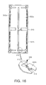
- FIG. 17 is a frontal sectional view showing the whole PCB sheet and a new good quality PCB sheet of FIG. 15.
- FIG. 2 is an exploded perspective view showing the coupling of the first and second PCB sheets, the sheets being fixed on the PCB securing plate according to the present invention.
- FIG. 3 is a schematic view showing the coupled state of the first and second PCB sheets according to the present invention.
- a first PCB sheet 4 a on which a plurality of circuit pattern parts 2 are printed is disposed on a PCB securing plate 1 .
- a second PCB sheet 4 b on which a good quality circuit pattern part 2 is printed is put to a place where a defective circuit pattern part 2 ′ of a first PCB sheet 4 a has been removed.
- the second PCB sheet 4 b is placed by being located by a PCB securing means 11 .
- the first and second PCB sheets 4 a and 4 b are fixed to the PCB securing plate 1 by means of PCB securing tapes 5 which are the constituents of the PCB securing means 11 . Thus any loose movements of the first and second PCB sheets 4 a and 4 b are prevented.
- a plurality of PCB securing pins 6 upstand on the PCB securing plate 1 , while the first and second PCB sheets 4 a and 4 b are provided with a plurality of pin receiving holes 7 correspondingly with the PCB securing pins 6 .
- the PCB securing pins 6 of the PCB securing plate 1 are inserted into the pin receiving holes 7 to support the PCB sheets 4 a and 4 b.
- a space 13 is formed between the first and second PCB sheets 4 a and 4 b , so that an adhesive 8 of an adhesive means 14 can be injected into a channel 9 of the space 13 .
- a tape 5 ′ is put to the bottom, front and rear of the channel 9 of the space 13 , so that the adhesive can be prevented from being leaked.
- a cover 10 covers the first and second PCB sheets 4 a and 4 b to protect the circuit patterns of the first and second PCB sheets 4 a and 4 b .
- the adhesive 8 which has been injected into the channel 9 is cured to couple the first and second PCB sheets 4 a and 4 b together.
- any one of the circuit pattern parts 2 which constitute a PCB sheet 3 is found to be defective upon testing by a tester (not illustrated), then the defective sheet part 4 ′ of the defective circuit pattern part 2 ′ is cut off by using a router or another cutter. Then a second PCB sheet 4 b on which a good quality circuit pattern part 2 is printed is prepared and is disposed to the cut space to be coupled with the first PCB sheet 4 a.
- the first PCB sheet 4 a which is coupled with the second PCB sheet 4 b is secured to the PCB securing plate 1 .
- the plurality of the PCB securing pins 6 are inserted into the plurality of the pin receiving holes 7 , with the result that the first and second PCB sheets 4 a and 4 b are supported on the PCB securing plate 1 , with the sheets 4 a and 4 b being separated by a certain distance.
- the first and second PCB sheets 4 a and 4 b are fixed to the PCB securing plate 1 by using a PCB securing tape 5 which is a both-face tape, so that any loose movements of the first and second PCB sheets 4 a and 4 b can be prevented.
- a PCB securing tape 5 which is a both-face tape
- the separation distance L between the first and second PCB sheets 4 a and 4 b is less than 1 mm, then the first and second PCB sheets 4 a and 4 b cannot be sufficiently strongly coupled together.
- the separation distance L is more than 5 mm, although the first, and second PCB sheets 4 a and 4 b can be sufficiently strongly coupled together, the expensive adhesive is too much consumed, and therefore, the economy is aggravated.
- the separation distance should be about 2 mm, and the volume of the injected adhesive 8 should be slightly smaller than or equal to the volume of the channel 9 .
- the first and second PCB sheets 4 a and 4 b are secured by using the PCB securing tape 5 and the tape 5 ′, the latter surrounding the channel 9 of the space 13 .
- the adhesive 8 is injected into the channel 9 of the space 13 which is formed between the first and second PCB sheets 4 a and 4 b .
- the whole structure is transferred to a drying furnace to make the adhesive 8 cured at a temperature of 120-200° C. Under this condition, the volatile component of the adhesive 8 has been removed in advance, and therefore, the thermal deformations such as the thermal expansion and the thermal contraction are made to be minimal.
- a hardening agent such as a highly heat resistant epoxy resin is added to the adhesive, and the proportion of the hardening agent is 1-5 wt % as against 99-95 wt % of the adhesive.
- the circuit patterns of the first and second PCB sheets 4 a and 4 b are covered with a flat cover part 10 to protect the first and second PCB sheets 4 a and 4 b from the heat.
- the adhesive 8 which has been injected into the channel 9 is exposed to the outside so as to be cured.
- the whole structure which consists of the first and second PCB sheets 4 a and 4 b and the PCB securing plate 1 is transferred to a drying furnace to make the adhesive 8 cured at a temperature of 120-200° C.
- the tape 5 ′ is removed from around the channel 9 , and the PCB securing plate 1 is separated from the first and second PCB sheets 4 a and 4 b , thereby completing the coupling of the first and second PCB sheets 4 a and 4 b together.
- FIGS. 6 and 7 illustrate a state in which the second PCB sheet is inserted into the first PCB sheet, and the two sheets are fixed onto the PCB securing plate, in a second embodiment of the present invention.
- FIG. 8 illustrates in detail the coupling portion of the first and second PCB sheets according to the present invention.
- any one of continuously printed circuit pattern parts 102 (printed on a first PCB sheet 104 ) is found to be a defective circuit pattern part 102 ′, then the rectangular portion of the defective circuit pattern part 102 ′ which is defined by a separation groove K is cut off by using a router or the like to form a blanked space S. Then a second PCB sheet 104 ′ with a new good quality circuit pattern 102 printed thereon is placed into the rectangular space S, and then, the first and second PCB sheets 104 and 104 ′ are located by using a PCB securing means 110 .
- the first and second PCB sheets 104 and 104 ′ are installed on the PCB securing plate 101 by using a PCB securing tape 105 which is one of the elements of the PCB securing means 110 .
- a plurality of PCB securing pins 106 upstand upon the PCB securing plate 101 , while the first and second PCB sheets 104 and 104 ′ are provided with a plurality of pin receiving holes 107 correspondingly with the PCB securing pins 106 .
- the PCB securing pins 106 and the pin receiving holes 107 constitute a PCB position locating means 120 .
- the PCB securing pins 106 of the PCB securing plate 101 are inserted into the pin receiving holes 107 to support the PCB sheets 104 and 104 ′.
- a cover part 10 is put on the first and second PCB sheets 104 and 104 ′ which are secured on the PCB securing plate 101 like in the first embodiment.
- the circuit pattern part 102 of the first and second PCB sheets 104 and 104 ′ are protected from the heat.
- the adhesive 108 is injected into the channel 109 , and the injected adhesive 108 is exposed to the outside so as to be cured. In this manner, the first and second PCB sheets 104 and 104 ′ are coupled together.
- any one of the circuit pattern parts 102 of the PCB sheet 103 is found be a defective circuit pattern part 102 ′, then the defective circuit pattern part 102 ′ is cut away along the groove K to form a blanked space S like in the first embodiment. Then a second PCB sheet 104 ′ on which a good quality circuit pattern part 102 is printed is placed into the blanked space S, and then, the second PCB sheet 104 ′ is coupled to the first PCB sheet 104 .
- the reason why the blanked space S is formed in a rectangular shape is as follows. That is, when the finished PCB product is carried to a subsequent process to install chip components and other electronic components, the weakness of the coupling portion between the first and second PCB sheets 104 and 104 ′ is reinforced by providing a rectangular blanked space, because the rectangular space increases the coupling area.
- a second PCB sheet 104 ′ on which a good quality circuit pattern is printed is placed into the blanked space S of the first PCB sheet 104 .
- the whole structure including the first and second PCB sheets 104 and 104 ′ is disposed on the PCB securing plate 101 to be secured on it.
- the PCB securing pins 106 of the PCB securing plate 101 are inserted into the pin receiving holes 107 to support the PCB sheets 104 and 104 ′, so that the first and second PCB sheets 104 and 104 ′ would be secured on the PCB securing plate 101 .
- a PCB securing tape 105 which is a both-face tape is put to around the coupling portion between the first and second PCB sheets 104 and 104 ′ and on the bottom of the PCB sheet so as to be attached on the PCB securing plate 101 .
- first and second PCB sheets 104 and 104 ′ which are disposed on the PCB securing plate 101 , there is provided a separation distance of about 1-5 mm.
- a space 130 which forms a channel 109 .
- a heat resistant tape 105 ′ is put to the bottom, front and rear of the channel 109 , so that the injected adhesive can be prevented from being leaked.
- the first and second PCB sheets 104 and 104 ′ are secured by using the PCB securing tape 105 and the tape 105 ′, the latter surrounding the channel 9 of the space 13 .
- the adhesive 108 is injected into the channel 109 of the space 130 which is formed between the first and second PCB sheets 104 and 104 ′.
- the whole structure is transferred to a drying furnace to make the adhesive 108 cured.
- a hardening agent such as a highly heat resistant epoxy resin is added to the adhesive.
- the circuit patterns of the first and second PCB sheets 104 and 104 ′ are covered with a flat cover part 10 to protect the first and second PCB sheets 104 and 104 ′ from the heat like in the first embodiment.
- the tape 105 which has been put to around the PCB sheet 104 ′ is removed, and the tape 105 ′ which has been put on the bottom of the channel 109 is also removed.
- the PCB securing plate 101 is separated from the first and second PCB sheets 104 and 104 ′, thereby completing the coupling of the first and second PCB sheets 104 and 104 ′.
- FIG. 10 illustrates a state in which a good quality PCB sheet is inserted into the whole PCB sheet, and the two sheets are fixed onto the PCB securing plate, in a third embodiment of the present invention.
- FIG. 11 illustrates a state in which a good quality PCB sheet is coupled into a space formed by the removal of the defective PCB sheet in the third embodiment of the present invention.
- a PCB sheet 204 on which a plurality of PCBs 202 are connectedly installed through a plurality of connecting parts 220 is disposed a PCB securing plate 201 . If a defective PCB 202 ′ is found among the plurality of the PCBs 202 , then the defective PCB 202 ′ is cut out along a PCB separating groove K. Then a good quality PCB 221 with connecting parts 220 ′ is fitted into the cut-out space 222 to be secured to the PCB sheet.
- the removal of the defective PCB 202 ′ is carried out in the following manner. That is, either a cutting is carried out around the connecting parts 220 (as shown in FIG. 2A), or the plurality of the connecting parts 220 of the PCB 202 are cut off (FIG. 2B).
- the reason is as follows. That is, when carrying the PCB sheets to a subsequent process, the carrying posture becomes different depending on the circuit pattern arrangement direction on the PCB sheet. Therefore, when installing chip components or other electronic components into the PCB 202 of the PCB sheet 204 , the joining portion of the good quality PCB 221 has to be made to have a high strength. For this purpose, the joining portion is selectively made long or short.
- a PCB securing tape 205 which is a both-face tape is put around and on the bottom of the coupling portion of the good quality PCB 221 to prevent any loose movements of the PCB sheet 204 and the good quality PCB 221 .
- the PCB sheet 204 and the good quality PCB 221 are fixed to the PCB securing plate 201 .
- a plurality of PCB securing pins 206 upstand upon the PCB securing plate 201 , while the PCB sheet 204 and the good quality PCB 221 are provided with a plurality of pin receiving holes 207 correspondingly with the PCB securing pins 206 . These pins and holes are for locating each of the PCB sheets 204 at exact position and are for carrying the PCB sheets 204 .
- a cover 210 is covered on the good quality PCB 221 and the PCB 202 of the PCB sheet 204 which is secured on the PCB securing plate 201 .
- the PCBs 202 of the PCB sheet 204 are protected from the ambient heat, and the adhesive 208 is injected into the channel 209 to be cured, thereby coupling a second PCB sheet 204 ′ (with the good quality PCB 221 printed thereon) to the first PCB sheet 204 .
- FIGS. 14 and 15 illustrate a state in which a good quality PCB sheet is inserted into the whole PCB sheet, and the two sheets are fixed onto the PCB securing plate by using a securing jig, in a fourth embodiment of the present invention.
- FIG. 16 is a plan view showing the coupling of a new good quality PCB sheet to the whole PCB sheet of FIG. 15.
- a PCB 303 consists of a plurality of circuit pattern parts 302 a which are connected to each other by connecting parts 301 . If a defective circuit pattern part is found among the plurality of the circuit pattern parts 302 a upon carrying out a testing, then the defective circuit pattern part is removed by cutting a connecting part 301 ′. In the place of the removed defective circuit pattern part, there is placed a good quality circuit pattern part 302 b by means of a PCB securing means 311 into a PCB securing jig 310 which has a plurality of separating walls 315 .
- the good quality circuit pattern part 302 b has to be secured in the place of the removed defective circuit pattern part.
- a PCB securing tape 305 which is a both-face tape is put on the bottom of the coupling portion, so that any loose movements of the good quality circuit pattern part 302 b can be prevented, thereby securing it to the PCB securing jig 310 .
- a plurality of PCB securing pins 306 upstand upon the PCB securing jig 310 , while the PCB 303 and the good quality circuit pattern part 302 b are provided with a plurality of pin receiving holes 307 .
- the plurality of the PCB securing pins 306 and the plurality of the pin receiving holes 307 constitute a PCB position locating means 312 .
- the PCB securing pins 306 of the PCB securing jig 310 are inserted into the pin receiving holes 307 of the PCB 303 and the good quality circuit pattern part 302 b .
- the good quality circuit pattern part 302 b is secured at a side of the PCB 303 within the PCB securing jig 310 .
- a cover 309 covers the good quality circuit pattern part 302 b and the PCB 303 on which a plurality of circuit patterns 302 a are formed. In this manner, the good quality circuit pattern part 302 b and the PCB 303 are protected from the ambient heat. Meanwhile, the adhesive 308 which has been injected into the channel of the space 313 is cured by being exposed to the external air, so that the good quality circuit pattern part 302 b can be firmly coupled to the PCB 303 .
- the defective circuit pattern is removed to replace it with a good quality circuit pattern so as to secure it in place in an easy manner.
- the whole PCB sheet which is otherwise to be discarded can be saved, thereby increasing the product yield and curtailing the production cost. That is, the PCB sheet on which a defective circuit pattern is printed is cut off, and the cut space is filled with a good quality circuit pattern sheet by means of a position locating means. Then a heat resistant tape and an adhesive means are used to secure the good quality circuit pattern sheet to the whole PCB sheet in an easy manner. Accordingly, in manufacturing the printed circuit board of the present invention, the workability and the productivity are drastically improved.
Landscapes
- Engineering & Computer Science (AREA)
- Chemical & Material Sciences (AREA)
- Chemical Kinetics & Catalysis (AREA)
- General Physics & Mathematics (AREA)
- Physics & Mathematics (AREA)
- Microelectronics & Electronic Packaging (AREA)
- Manufacturing & Machinery (AREA)
- Pathology (AREA)
- General Health & Medical Sciences (AREA)
- Immunology (AREA)
- Biochemistry (AREA)
- Analytical Chemistry (AREA)
- Life Sciences & Earth Sciences (AREA)
- Health & Medical Sciences (AREA)
- Ceramic Engineering (AREA)
- Condensed Matter Physics & Semiconductors (AREA)
- Computer Hardware Design (AREA)
- Power Engineering (AREA)
- Structure Of Printed Boards (AREA)
- Combinations Of Printed Boards (AREA)
Abstract
A method and a device for coupling a PCB sheet are disclosed. If a defective PCB is found after the manufacture of continuously arranged circuit patterns, then the defective PCB sheet portion is removed to replace it with a new PCB sheet portion. That is, a defective circuit pattern sheet 2′ is removed from continuously arranged circuit patterns of a first PCB sheet 4 a. After removal of the defective circuit pattern sheet 2′, the first PCB sheet 4 a is position-located by means of a position locating means 12. Then the space which is formed by removing the defective circuit pattern sheet 2′ is filled with a second PCB sheet 4 b on which a good quality circuit pattern 2 b is printed. Then the first PCB sheet 4 a and the second PCB sheet 4 b are coupled together by using an adhesive means 14.
Description
- 1. Field of the Invention
- The present invention relates to a method and a device for coupling a printed circuit board (to be called PCB below) sheet, in which a plurality of PCBs are continuously arranged on a sheet when manufacturing the PCBs, and if a defective PCB is found after the manufacture, then the defective PCB sheet portion is removed to replace it with a new PCB sheet portion. Particularly, the present invention relates to a method and a device for coupling a PCB sheet, in which in a continuously printed PCBs on a sheet, a defective portion is removed, a first PCB sheet formed by the removal is located by a position locating means to be filled with a second PCB sheet of a good quality circuit pattern, and an adhesive material is spread on a space area between the first PCB sheet and a second PCB sheet, thereby making the arrangement of the PCBs continuous. Thus the defective PCB is removed, and a good quality PCB is replaced into the place in an easy manner, so that the defective PCB can be turned to a good quality portion.
- 2. Description of the Prior Art
- Generally, as shown in FIG. 1, in the conventional PCB sheet structure, a plurality of
circuit patterns PCB sheet 52. - In this
conventional PCB sheet 52, the plurality of thecircuit patterns acceptable PCB sheets 52 are used as the final product. However, if anyone of the plurality of the circuit patterns is defective, then the whole PCB sheet on which the plurality of thecircuit patterns - That is, if any one of the plurality of the circuit patterns is found to be defective upon inspecting them, even the good circuit patterns have to be discarded.
- As a result, the material loss is high because of the discarding of the total sheet, and the workability and productivity are aggravated, as well as increasing the production cost.
- The present invention is intended to overcome the above described disadvantages of the conventional technique.
- Therefore it is an object of the present invention to provide a device for coupling a PCB sheet, in which defective circuit pattern portions are removed from a continuously arranged circuit pattern sheet to replace with new ones, so that a whole circuit pattern sheet can be saved without being discarded, thereby increasing the product yield, and curtailing the production cost.
- It is another object of the present invention to provide a method for coupling a PCB sheet, in which defective circuit pattern portions are cut away from a continuously arranged circuit pattern sheet, and the cut space is filled with new ones by using a position locating means, the filling being carried out in a simple manner by using a heat resistant tape and an adhesive means containing a hardening agent, thereby improving the workability and the productivity.
- In achieving the above objects, the device for coupling a PCB sheet according to the present invention includes:
- a position locating means disposed upon a PCB securing plate, for locating the position of a second PCB sheet of a good quality circuit pattern to fill a space after removing a PCB sheet of a defective circuit pattern from a continuously arranged circuit patterns of a first PCB sheet; a PCB securing means attached on the PCB securing plate, for preventing loose movements of the first and second PCB sheets; a space for putting an adhesive means into between the first and second PCB sheets (which are secured on the PCB securing plate); and the adhesive means being filled into the space between the first and second PCB sheets to be cured so as to couple the first and second PCB sheets together.
- In another aspect of the present invention, the method for coupling a PCB sheet according to the present invention includes the steps of: cutting a defective PCB sheet of a defective circuit pattern to remove it from a continuously arranged circuit patterns of a first PCB sheet (defective circuit pattern removing step); filling a vacant place of the removed defective PCB sheet with a second PCB sheet of a good quality circuit pattern by utilizing a position locating means (PCB sheet position locating step); placing the first and second PCB sheets on a PCB securing plate by using a PCB securing means to prevent any loose movements of them, and filling an adhesive (with a volatile component being removed) into a space between the first and second PCB sheets to cure the adhesive at a temperature of 120-200° C. within a drying furnace (adhesive injecting and curing step); and removing the position locating means to separate the PCB securing plate from the PCB sheet after a curing of the adhesive (PCB securing plate separating step).
- The above objects and other advantages of the present invention will become more apparent by describing in detail the preferred embodiment of the present invention with reference to the attached drawings in which:
- FIG. 1 is a perspective view of the general PCB sheet in which circuit patterns are continuously printed on a sheet;
- FIG. 2 is an exploded perspective view showing the coupling of the first and second PCB sheets, the sheets being fixed on the PCB securing plate according to the present invention;
- FIG. 3 is a schematic view showing the coupled state of the first and second PCB sheets according to the present invention;
- FIG. 4 illustrates in detail the coupling portion of the first and second PCB sheets according to the present invention;
- FIG. 5 is a frontal sectional view showing the coupled state of the first and second PCB sheets according to the present invention;
- FIG. 6 illustrates a state in which the second PCB sheet is inserted into the first PCB sheet, and the two sheets are fixed onto the PCB securing plate, in a second embodiment of the present invention;
- FIG. 7 is a schematic perspective view showing the coupled state of the first and second PCB sheets in the second embodiment of the present invention;
- FIG. 8 illustrates in detail the coupling portion of the first and second PCB sheets according to the present invention;
- FIG. 9 is a frontal sectional view showing the coupled state of the first and second PCB sheets of FIG. 8;
- FIG. 10 illustrates a state in which a good quality PCB sheet is inserted into the whole PCB sheet, and the two sheets are fixed onto the PCB securing plate, in a third embodiment of the present invention;
- FIG. 11 illustrates a state in which a good quality PCB sheet is coupled into a space formed by the removal of the defective PCB sheet in the third embodiment of the present invention;
- FIGS. 12A and 12B are plan views showing the coupling of a new good quality PCB sheet to the whole PCB sheet in the third embodiment of the present invention;
- FIG. 13 is a frontal sectional view showing the whole PCB sheet and a new good quality PCB sheet;
- FIG. 14 illustrates a state in which a good quality PCB sheet is inserted into the whole PCB sheet, and the two sheets are fixed onto the PCB securing plate by using a securing jig, in a fourth embodiment of the present invention;
- FIG. 15 is a schematic perspective view showing the coupling of a new good quality PCB sheet to the whole PCB sheet in the fourth embodiment of the present invention;
- FIG. 16 is a plan view showing the coupling of a new good quality PCB sheet to the whole PCB sheet of FIG. 15; and
- FIG. 17 is a frontal sectional view showing the whole PCB sheet and a new good quality PCB sheet of FIG. 15.
- The preferred embodiments of the present invention will be described referring to the attached drawings.
- FIG. 2 is an exploded perspective view showing the coupling of the first and second PCB sheets, the sheets being fixed on the PCB securing plate according to the present invention. FIG. 3 is a schematic view showing the coupled state of the first and second PCB sheets according to the present invention.
- A
first PCB sheet 4 a on which a plurality ofcircuit pattern parts 2 are printed is disposed on a PCB securingplate 1. Asecond PCB sheet 4 b on which a good qualitycircuit pattern part 2 is printed is put to a place where a defectivecircuit pattern part 2′ of afirst PCB sheet 4 a has been removed. Thesecond PCB sheet 4 b is placed by being located by a PCB securing means 11. - The first and
second PCB sheets PCB securing plate 1 by means ofPCB securing tapes 5 which are the constituents of the PCB securing means 11. Thus any loose movements of the first andsecond PCB sheets - A plurality of
PCB securing pins 6 upstand on thePCB securing plate 1, while the first andsecond PCB sheets pin receiving holes 7 correspondingly with the PCB securingpins 6. Thus the PCB securingpins 6 of thePCB securing plate 1 are inserted into thepin receiving holes 7 to support thePCB sheets - A
space 13 is formed between the first andsecond PCB sheets channel 9 of thespace 13. Atape 5′ is put to the bottom, front and rear of thechannel 9 of thespace 13, so that the adhesive can be prevented from being leaked. - A
cover 10 covers the first andsecond PCB sheets second PCB sheets adhesive 8 which has been injected into thechannel 9 is cured to couple the first andsecond PCB sheets - Now the method for the PCB sheet according to the present invention will be described.
- As shown in FIGS. 2 to 5, if any one of the
circuit pattern parts 2 which constitute aPCB sheet 3 is found to be defective upon testing by a tester (not illustrated), then thedefective sheet part 4′ of the defectivecircuit pattern part 2′ is cut off by using a router or another cutter. Then asecond PCB sheet 4 b on which a good qualitycircuit pattern part 2 is printed is prepared and is disposed to the cut space to be coupled with thefirst PCB sheet 4 a. - Then the
first PCB sheet 4 a which is coupled with thesecond PCB sheet 4 b is secured to thePCB securing plate 1. Under this condition, the plurality of the PCB securingpins 6 are inserted into the plurality of thepin receiving holes 7, with the result that the first andsecond PCB sheets PCB securing plate 1, with thesheets - Then the first and
second PCB sheets PCB securing plate 1 by using a PCB securingtape 5 which is a both-face tape, so that any loose movements of the first andsecond PCB sheets tape 5 should be only minimally affected by the thermal deformation. That is, a heat resistant tape is used, so that the tape can be easily removed upon completion of the coupling of the first andsecond PCB sheets - Meanwhile, between the first and
second PCB sheets PCB securing plate 1, there is provided a separation distance L of about 1-5 mm. Thus there is formed aspace 13 which forms achannel 9. Then a heatresistant tape 5′ is put to the bottom, front and rear of thechannel 9, so that the injected adhesive can be prevented from being leaked. - If the separation distance L between the first and
second PCB sheets second PCB sheets second PCB sheets channel 9. - Thus the first and
second PCB sheets PCB securing tape 5 and thetape 5′, the latter surrounding thechannel 9 of thespace 13. Then the adhesive 8 is injected into thechannel 9 of thespace 13 which is formed between the first andsecond PCB sheets - After the injection of the adhesive 8, the circuit patterns of the first and
second PCB sheets flat cover part 10 to protect the first andsecond PCB sheets channel 9 is exposed to the outside so as to be cured. Then the whole structure which consists of the first andsecond PCB sheets PCB securing plate 1 is transferred to a drying furnace to make the adhesive 8 cured at a temperature of 120-200° C. - After the completion of the curing of the adhesive 8, the
tape 5′ is removed from around thechannel 9, and thePCB securing plate 1 is separated from the first andsecond PCB sheets second PCB sheets - FIGS. 6 and 7 illustrate a state in which the second PCB sheet is inserted into the first PCB sheet, and the two sheets are fixed onto the PCB securing plate, in a second embodiment of the present invention. FIG. 8 illustrates in detail the coupling portion of the first and second PCB sheets according to the present invention.
- If any one of continuously printed circuit pattern parts 102 (printed on a first PCB sheet 104) is found to be a defective
circuit pattern part 102′, then the rectangular portion of the defectivecircuit pattern part 102′ which is defined by a separation groove K is cut off by using a router or the like to form a blanked space S. Then asecond PCB sheet 104′ with a new goodquality circuit pattern 102 printed thereon is placed into the rectangular space S, and then, the first andsecond PCB sheets - The first and
second PCB sheets PCB securing plate 101 by using aPCB securing tape 105 which is one of the elements of the PCB securing means 110. - A plurality of
PCB securing pins 106 upstand upon thePCB securing plate 101, while the first andsecond PCB sheets pin receiving holes 107 correspondingly with the PCB securing pins 106. The PCB securing pins 106 and thepin receiving holes 107 constitute a PCB position locating means 120. Thus the PCB securing pins 106 of thePCB securing plate 101 are inserted into thepin receiving holes 107 to support thePCB sheets - Further as shown in FIG. 9, between the first and
second PCB sheets space 130 to form a channel 109, so that an adhesive 108 as an adhesive means 140 can be injected into the channel 109. On the bottom of the channel 109, there is put aPCB securing tape 105′ to prevent any leakage of the adhesive 108. - A
cover part 10 is put on the first andsecond PCB sheets PCB securing plate 101 like in the first embodiment. Thus thecircuit pattern part 102 of the first andsecond PCB sheets second PCB sheets - Accordingly, as shown in FIGS. 6 to 9, if any one of the
circuit pattern parts 102 of thePCB sheet 103 is found be a defectivecircuit pattern part 102′, then the defectivecircuit pattern part 102′ is cut away along the groove K to form a blanked space S like in the first embodiment. Then asecond PCB sheet 104′ on which a good qualitycircuit pattern part 102 is printed is placed into the blanked space S, and then, thesecond PCB sheet 104′ is coupled to thefirst PCB sheet 104. - Under this condition, the reason why the blanked space S is formed in a rectangular shape is as follows. That is, when the finished PCB product is carried to a subsequent process to install chip components and other electronic components, the weakness of the coupling portion between the first and
second PCB sheets - After completion of the blanking of the PCB sheet portion of the defective
circuit pattern part 102′, asecond PCB sheet 104′ on which a good quality circuit pattern is printed is placed into the blanked space S of thefirst PCB sheet 104. The whole structure including the first andsecond PCB sheets PCB securing plate 101 to be secured on it. Under this condition, the PCB securing pins 106 of thePCB securing plate 101 are inserted into thepin receiving holes 107 to support thePCB sheets second PCB sheets PCB securing plate 101. - In order to prevent any loose movements of the first and
second PCB sheets PCB securing tape 105 which is a both-face tape is put to around the coupling portion between the first andsecond PCB sheets PCB securing plate 101. - Further, between the first and
second PCB sheets PCB securing plate 101, there is provided a separation distance of about 1-5 mm. Thus there is formed aspace 130 which forms a channel 109. Then a heatresistant tape 105′ is put to the bottom, front and rear of the channel 109, so that the injected adhesive can be prevented from being leaked. - Thus the first and
second PCB sheets PCB securing tape 105 and thetape 105′, the latter surrounding thechannel 9 of thespace 13. Then the adhesive 108 is injected into the channel 109 of thespace 130 which is formed between the first andsecond PCB sheets second PCB sheets flat cover part 10 to protect the first andsecond PCB sheets - Then the
tape 105 which has been put to around thePCB sheet 104′ is removed, and thetape 105′ which has been put on the bottom of the channel 109 is also removed. Then, thePCB securing plate 101 is separated from the first andsecond PCB sheets second PCB sheets - FIG. 10 illustrates a state in which a good quality PCB sheet is inserted into the whole PCB sheet, and the two sheets are fixed onto the PCB securing plate, in a third embodiment of the present invention. FIG. 11 illustrates a state in which a good quality PCB sheet is coupled into a space formed by the removal of the defective PCB sheet in the third embodiment of the present invention.
- A
PCB sheet 204 on which a plurality ofPCBs 202 are connectedly installed through a plurality of connectingparts 220 is disposed aPCB securing plate 201. If adefective PCB 202′ is found among the plurality of thePCBs 202, then thedefective PCB 202′ is cut out along a PCB separating groove K. Then agood quality PCB 221 with connectingparts 220′ is fitted into the cut-out space 222 to be secured to the PCB sheet. - As shown in FIGS. 12A and 12B, the removal of the
defective PCB 202′ is carried out in the following manner. That is, either a cutting is carried out around the connecting parts 220 (as shown in FIG. 2A), or the plurality of the connectingparts 220 of thePCB 202 are cut off (FIG. 2B). The reason is as follows. That is, when carrying the PCB sheets to a subsequent process, the carrying posture becomes different depending on the circuit pattern arrangement direction on the PCB sheet. Therefore, when installing chip components or other electronic components into thePCB 202 of thePCB sheet 204, the joining portion of thegood quality PCB 221 has to be made to have a high strength. For this purpose, the joining portion is selectively made long or short. - As shown in FIG. 13, a
PCB securing tape 205 which is a both-face tape is put around and on the bottom of the coupling portion of thegood quality PCB 221 to prevent any loose movements of thePCB sheet 204 and thegood quality PCB 221. In this manner, thePCB sheet 204 and thegood quality PCB 221 are fixed to thePCB securing plate 201. - A plurality of
PCB securing pins 206 upstand upon thePCB securing plate 201, while thePCB sheet 204 and thegood quality PCB 221 are provided with a plurality ofpin receiving holes 207 correspondingly with the PCB securing pins 206. These pins and holes are for locating each of thePCB sheets 204 at exact position and are for carrying thePCB sheets 204. - Between the
PCB sheet 204 and thegood quality PCB 221, there is formed aspace 213 to form achannel 209, so that an adhesive 208 as an adhesive means 214 can be injected into thechannel 209. On the bottom, front and rear of thechannel 209, there is put aPCB securing tape 205′ to prevent any leakage of the adhesive 208. - Further, a
cover 210 is covered on thegood quality PCB 221 and thePCB 202 of thePCB sheet 204 which is secured on thePCB securing plate 201. Thus thePCBs 202 of thePCB sheet 204 are protected from the ambient heat, and the adhesive 208 is injected into thechannel 209 to be cured, thereby coupling asecond PCB sheet 204′ (with thegood quality PCB 221 printed thereon) to thefirst PCB sheet 204. - FIGS. 14 and 15 illustrate a state in which a good quality PCB sheet is inserted into the whole PCB sheet, and the two sheets are fixed onto the PCB securing plate by using a securing jig, in a fourth embodiment of the present invention. FIG. 16 is a plan view showing the coupling of a new good quality PCB sheet to the whole PCB sheet of FIG. 15.
- A
PCB 303 consists of a plurality ofcircuit pattern parts 302 a which are connected to each other by connectingparts 301. If a defective circuit pattern part is found among the plurality of thecircuit pattern parts 302 a upon carrying out a testing, then the defective circuit pattern part is removed by cutting a connectingpart 301′. In the place of the removed defective circuit pattern part, there is placed a good qualitycircuit pattern part 302 b by means of a PCB securing means 311 into aPCB securing jig 310 which has a plurality of separatingwalls 315. - As shown in FIG. 16, the good quality
circuit pattern part 302 b has to be secured in the place of the removed defective circuit pattern part. For this purpose, aPCB securing tape 305 which is a both-face tape is put on the bottom of the coupling portion, so that any loose movements of the good qualitycircuit pattern part 302 b can be prevented, thereby securing it to thePCB securing jig 310. - A plurality of
PCB securing pins 306 upstand upon thePCB securing jig 310, while thePCB 303 and the good qualitycircuit pattern part 302 b are provided with a plurality ofpin receiving holes 307. The plurality of the PCB securing pins 306 and the plurality of thepin receiving holes 307 constitute a PCB position locating means 312. Thus the PCB securing pins 306 of thePCB securing jig 310 are inserted into thepin receiving holes 307 of thePCB 303 and the good qualitycircuit pattern part 302 b. Thus the good qualitycircuit pattern part 302 b is secured at a side of thePCB 303 within thePCB securing jig 310. - Between the
PCB 303 and the good qualitycircuit pattern part 302 b, there is formed aspace 313 which forms a channel. An adhesive 308 which is an adhesive means 314 is injected to the channel. - As shown in FIG. 17, a
cover 309 covers the good qualitycircuit pattern part 302 b and thePCB 303 on which a plurality ofcircuit patterns 302 a are formed. In this manner, the good qualitycircuit pattern part 302 b and thePCB 303 are protected from the ambient heat. Meanwhile, the adhesive 308 which has been injected into the channel of thespace 313 is cured by being exposed to the external air, so that the good qualitycircuit pattern part 302 b can be firmly coupled to thePCB 303. - According to the present invention as described above, if a defective circuit pattern is found among the plurality of the circuit patterns, then the defective circuit pattern is removed to replace it with a good quality circuit pattern so as to secure it in place in an easy manner. By removing the defective circuit pattern, the whole PCB sheet which is otherwise to be discarded can be saved, thereby increasing the product yield and curtailing the production cost. That is, the PCB sheet on which a defective circuit pattern is printed is cut off, and the cut space is filled with a good quality circuit pattern sheet by means of a position locating means. Then a heat resistant tape and an adhesive means are used to secure the good quality circuit pattern sheet to the whole PCB sheet in an easy manner. Accordingly, in manufacturing the printed circuit board of the present invention, the workability and the productivity are drastically improved.
- In the above, the present invention was described based on the specific embodiments and the attached drawings, but it should be apparent to those ordinarily skilled in the art that various changes and modification can be added without departing from the spirit and scope of the present invention which will be defined by the appended claims.
Claims (34)
1. A device for coupling a PCB sheet, comprising:
a position locating means 12 disposed upon a PCB securing plate 1, for locating a position of a second PCB sheet 4 b of a good quality circuit pattern 2 b to fill a space after removing a PCB sheet 4′ of a defective circuit pattern 2′ from a continuously arranged circuit patterns 2 a of a first PCB sheet 4 a;
a PCB securing means 11 attached on said PCB securing plate 1, for preventing any loose movements of said first and second PCB sheets 4 a and 4 b;
a space 13 for receiving an adhesive means 14, and formed between said first and second PCB sheets 4 a and 4 b (which are secured on said PCB securing plate 1); and
said adhesive means 14 being filled into said space 13 between said first and second PCB sheets 4 a and 4 b to be cured so as to couple said first and second PCB sheets 4 a and 4 b together.
2. The device as claimed in claim 1 , wherein said position locating means 12 for locating positions of said first and second PCB sheets 4 a and 4 b on said PCB securing plate 1 comprises a plurality of PCB securing pins 6 upstanding on said PCB securing plate 1 and a plurality of pin receiving holes 7, for carrying said first and second PCB sheets 4 a and 4 b, with said pins 6 being inserted into said holes 7.
3. The device as claimed in claim 1 , wherein said PCB securing means 11 for securing said first and second PCB sheets 4 a and 4 b on said PCB securing plate 1 consists of PCB securing tapes 5.
4. The device as claimed in claim 3 , wherein said PCB securing tapes 5 are both-face tapes, and are put around and on a bottom of said first and second PCB sheets 4 a and 4 b and said PCB securing plate 1.
5. The device as claimed in any one of claims 3 and 4, wherein said PCB securing tapes 5 are heat resistant tapes for preventing thermal deformations.
6. The device as claimed in claim 1 , wherein said space 13 formed between said first and second PCB sheets 4 a and 4 b forms a channel 9.
7. The device as claimed in claim 1 , wherein said adhesive means 14 filled into said space 13 between said first and second PCB sheets 4 a and 4 b is a high temperature adhesive 8 for preventing thermal deformations.
8. The device as claimed in claim 6 , wherein a PCB securing tape 5′ is put to a bottom, front and rear of said channel 9, for preventing a leakage of said adhesive 8.
9. The device as claimed in claim 1 , further comprising a flat cover 10 disposed on said first and second PCB sheets 4 a and 4 b to protect them from an ambient heat.
10. The device as claimed in claim 7 , wherein a hardening agent is added to said adhesive 8.
11. The device as claimed in claim 1 , wherein said space 13 formed between said first and second PCB sheets 4 a and 4 b for receiving said adhesive 8 has a width of 1-5 mm between said first and second PCB sheets 4 a and 4 b.
12. A method for coupling a PCB sheet, comprising the steps of:
cutting away a defective PCB sheet of a defective circuit pattern to remove it from a continuously arranged circuit patterns of a first PCB sheet (defective circuit pattern removing step);
filling a vacant place of said removed defective PCB sheet with a second PCB sheet of a good quality circuit pattern by utilizing a position locating means (PCB sheet position locating step);
placing said first and second PCB sheets on a PCB securing plate by using a PCB securing means to prevent any loose movements of them, and filling an adhesive (with a volatile component being removed) into a space between said first and second PCB sheets to cure said adhesive at a temperature of 120-200° C. within a drying furnace (adhesive injecting and curing step); and
removing said position locating means to separate said PCB securing plate from said PCB sheet after a curing of said adhesive (PCB securing plate separating step).
13. The method as claimed in claim 12 , wherein said second PCB sheet replaced into a space of said defective circuit pattern is decided into place by means of PCB securing pins of said PCB securing plate and pin receiving holes of said first and second PCB sheets.
14. The method as claimed in claim 12 , wherein a heat resistant PCB securing tape is put around and on bottom of said first and second PCB sheets to prevent any loose movements of them.
15. The method as claimed in claim 12 , wherein said adhesive injected into said channel between said first and second PCB sheets is cured at a temperature of 120-200° C.
16. The method as claimed in claim 12 , wherein said adhesive injected into said channel between said first and second PCB sheets is a heat resistant epoxy resin for preventing any thermal deformations.
17. The method as claimed in claim 12 , wherein a hardening agent is added in an amount of 1-5 wt % as against 99-95 wt % of said adhesive.
18. The method as claimed in claim 12 , further comprising a flat cover disposed on said first and second PCB sheets to protect them.
19. The method as claimed in claim 12 , wherein said adhesive injected into said channel between said first and second PCB sheets is exposed to an external air.
20. The method as claimed in claim 12 , wherein said adhesive injected into said channel between said first and second PCB sheets is injected in a volume equal to or smaller than a volume of said channel.
21. A device for coupling a PCB sheet, comprising:
a blanked space forming part 112 for forming a blanked space S by cutting away a defective circuit pattern part 102′ if any one of circuit pattern parts 102 of a first PCB sheet 104 is found be a defective circuit pattern part 102′, and placing into said blanked space S a second PCB sheet 104′ on which a good quality circuit pattern part 102 is printed, and inserting PCB securing pins 106 of a PCB securing plate 101 into pin receiving holes 107 so as to position-locate said first and second PCB sheets 104 and 104′;
a PCB securing means 111 attached on said PCB securing plate 101, for preventing any loose movements of said first and second PCB sheets 104 and 104′;
a space 113 formed between said first and second PCB sheets 104 and 104′, for receiving an adhesive means 140 into between said first and second PCB sheets 104 and 104′ (which are secured on said PCB securing plate 101); and
said adhesive means 140 being filled into said space 113 between said first and second PCB sheets 104 and 104′ to be cured so as to couple said first and second PCB sheets 104 and 104′ together.
22. The device as claimed in claim 21 , further comprising a flat cover 10 disposed on said first and second PCB sheets 104 and 104′ to protect them.
23. A method for coupling a PCB sheet, comprising the steps of:
cutting away a defective PCB sheet of a defective circuit pattern to remove it along a separating groove from a continuously arranged circuit patterns of a first PCB sheet so as to form a blanked space (defective circuit pattern removing step);
filling said blanked space of said removed defective PCB sheet with a second PCB sheet of a good quality circuit pattern by utilizing a position locating means so as to position-locate said first and second PCB sheets on a PCB securing plate (PCB sheet position locating step);
placing said first and second PCB sheets on said PCB securing plate by using a PCB securing means to prevent any loose movements of them, that is, by using PCB securing tapes (PCB sheet securing step);
filling an adhesive (with a volatile component being removed) into a space between said first and second PCB sheets to cure said adhesive at a temperature of 120-200° C. within a drying furnace (adhesive injecting and curing step); and
putting a cover on said first and second PCB sheets to protect them from an ambient heat, and removing said position locating means and said PCB securing tapes to separate said PCB securing plate from said PCB sheet after a curing of said adhesive (PCB securing plate separating step).
24. The method as claimed in claim 23 , wherein said second PCB sheet replaced into a space of said defective circuit pattern is decided into place by means of PCB securing pins of said PCB securing plate and pin receiving holes of said first and second PCB sheets.
25. The method as claimed in claim 23 , wherein said adhesive injected into said channel between said first and second PCB sheets is cured at a temperature of 120-200° C.
26. The method as claimed in claim 23 , wherein a hardening agent is added in an amount of 1-5 wt % as against 99-95 wt % of said adhesive.
27. A device for coupling a PCB sheet, comprising:
a PCB position locating means 212 for position-locating a PCB 202 and a replaced good quality PCB 221 of a PCB sheet 204 by inserting PCB securing pins 206 of a PCB securing plate 201 into pin receiving holes 207 of said PCB 202 and a replaced good quality PCB 221 after a defective circuit pattern has been removed by being cut along a separating groove K to form a blanked space 222, and after said good quality PCB 221 integrally with connecting parts 220′ has been replaced into said blanked space 222;
a PCB securing means 211 attached on said PCB securing plate 201, for preventing any loose movements of said PCB sheet 204 and said PCB 221 of said good quality circuit pattern;
a space 213 formed between said PCB sheet 204 and said replaced good quality PCB 221, for forming a channel 209; and
an adhesive means 214 filled into said channel 209 of said space 213 between said PCB sheet 204 and said replaced good quality PCB 221 to be cured so as to couple them together.
28. A method for coupling a PCB sheet, comprising the steps of:
cutting away a defective PCB sheet of a defective circuit pattern to remove it along a separating groove from a continuously arranged circuit patterns of a PCB sheet so as to form a blanked space (blanked space forming step);
filling said blanked space of said removed defective PCB sheet with a good quality circuit pattern integrally with connecting parts by utilizing a position locating means so as to position-locate said PCB sheet and said good quality pattern sheet on a PCB securing plate (PCB sheet position locating step);
fixing said PCB sheet and said good quality circuit pattern sheet on said PCB securing plate by using a PCB securing means to prevent any loose movements of them, that is, by using PCB securing tapes, and filling an adhesive (with a volatile component being removed) of an epoxy resin into a space between said PCB sheet and said good quality circuit pattern sheet to cure said adhesive at a temperature of 120-200° C. within a drying furnace (adhesive injecting and curing step); and
putting a cover on said PCB sheet and said good quality circuit pattern sheet to protect them from an ambient heat, and removing said position locating means and said PCB securing tapes to separate said PCB securing plate from said PCB sheet after a curing of said adhesive, thereby completing a coupling of said PCB sheet and said good quality circuit pattern sheet (PCB securing plate separating step).
29. The method as claimed in claim 28 , wherein the PCB sheet position locating step is carried out by inserting PCB securing pins of said PCB securing plate into pin receiving holes of said PCB sheet and said good quality circuit pattern sheet.
30. A device for coupling a PCB sheet, comprising:
a position deciding jig part for receiving a PCB sheet (with a plurality of circuit patterns printed thereon) and a replaced good quality circuit pattern sheet, after a defective circuit pattern sheet is cut away, and after said good quality circuit pattern sheet is placed into a space of said removed defective circuit pattern sheet;
a PCB securing means attached on said PCB securing plate, for preventing any loose movements of said PCB sheet and said good quality circuit pattern sheet, both of them inserted into said jig part; and
an adhesive means filled into a space between said PCB sheet and said replaced good quality circuit pattern sheet to be cured so as to couple them together.
31. The device as claimed in claim 30 , further comprising a position locating means 312, said position locating means 312 consisting of a plurality of PCB securing pins 306 upstanding on said PCB securing jig part 310, and a plurality of pin receiving holes 307 formed in said PCB sheet 303 and on said good quality circuit pattern sheet, said PCB securing pins 306 being inserted into said pin receiving holes 307.
32. The device as claimed in claim 30 , wherein said PCB securing jig part 310 comprises a plurality of separating walls 315 to separate said sheets of said PCB sheet and said good quality circuit pattern sheet from each other.
33. A method for coupling a PCB sheet, comprising the steps of:
cutting connecting parts of a defective circuit pattern sheet to remove it from a continuously arranged circuit patterns of a PCB sheet (defective circuit pattern sheet removing step);
filling a vacant place of said removed defective circuit pattern sheet with a good quality circuit pattern sheet to be placed into a PCB securing jig part together with said PCB sheet, said connecting parts forming a gap respectively so as to be position-decided (PCB sheet position locating step);
placing said PCB sheet and said good quality circuit pattern sheet into said PCB securing jig part and putting heat resistant tapes on bottoms of said PCB sheet and said good quality circuit pattern sheet to prevent nay loose movements of them, thereby securing said PCB sheet and said good quality circuit pattern sheet on said PCB securing jig part (PCB securing step);
filling an adhesive (with a volatile component being removed) of an epoxy resin into a space between said PCB sheet and said good quality circuit pattern sheet to cure said adhesive at a temperature of 120-200° C. within a drying furnace (adhesive injecting and curing step); and
putting a cover on said PCB sheet and on said good quality circuit pattern sheet to protect them from an ambient heat, and removing said position locating means and said PCB securing tapes after a curing of said adhesive to separate said PCB securing plate from said PCB sheet after a curing of said adhesive, thereby completing a coupling of said PCB sheet and said good quality circuit pattern sheet together (PCB securing plate separating step).
34. The method as claimed in claim 33 , wherein said adhesive injected into a channel between said PCB sheet and said good quality circuit pattern sheet is a heat resistant epoxy resin to avoid thermal deformations; and
a hardening agent is added in an amount of 1-5 wt % as against 99-95 wt % of said adhesive.
Priority Applications (4)
| Application Number | Priority Date | Filing Date | Title |
|---|---|---|---|
| US10/177,664 US7017248B2 (en) | 1999-02-23 | 2002-06-24 | Device for coupling PCB sheet |
| US11/038,050 US7234217B2 (en) | 1999-02-23 | 2005-01-21 | Device for coupling PCB sheet having position deciding jig part |
| US11/038,048 US7278193B2 (en) | 1999-02-23 | 2005-01-21 | Device for coupling PCB sheet |
| US11/038,047 US7103966B2 (en) | 1999-02-23 | 2005-01-21 | Device for coupling PCB sheet |
Applications Claiming Priority (12)
| Application Number | Priority Date | Filing Date | Title |
|---|---|---|---|
| KR1019990005914A KR100298907B1 (en) | 1998-02-26 | 1999-02-23 | method and device for combine of PCB sheet |
| KR1999-05914 | 1999-02-23 | ||
| KR1999-43716 | 1999-10-11 | ||
| KR1019990043715A KR100332868B1 (en) | 1999-10-11 | 1999-10-11 | method and device for combine of PCB sheet |
| KR1019990043717A KR100332870B1 (en) | 1999-10-11 | 1999-10-11 | method and device for combine of PCB |
| KR1999-43717 | 1999-10-11 | ||
| KR1999-43715 | 1999-10-11 | ||
| KR1019990043716A KR100332869B1 (en) | 1999-10-11 | 1999-10-11 | method and device for combine of PCB sheet |
| KR1019990043714A KR100332867B1 (en) | 1999-10-11 | 1999-10-11 | method and device for combine of PCB sheet |
| KR1999-43714 | 1999-10-11 | ||
| US09/510,298 US6574862B1 (en) | 1999-02-23 | 2000-02-22 | Method for coupling PCB sheet |
| US10/177,664 US7017248B2 (en) | 1999-02-23 | 2002-06-24 | Device for coupling PCB sheet |
Related Parent Applications (1)
| Application Number | Title | Priority Date | Filing Date |
|---|---|---|---|
| US09/510,298 Division US6574862B1 (en) | 1999-02-23 | 2000-02-22 | Method for coupling PCB sheet |
Related Child Applications (4)
| Application Number | Title | Priority Date | Filing Date |
|---|---|---|---|
| US11/038,048 Division US7278193B2 (en) | 1999-02-23 | 2005-01-21 | Device for coupling PCB sheet |
| US11/038,047 Division US7103966B2 (en) | 1999-02-23 | 2005-01-21 | Device for coupling PCB sheet |
| US11/038,050 Division US7234217B2 (en) | 1999-02-23 | 2005-01-21 | Device for coupling PCB sheet having position deciding jig part |
| US11/038,050 Continuation US7234217B2 (en) | 1999-02-23 | 2005-01-21 | Device for coupling PCB sheet having position deciding jig part |
Publications (2)
| Publication Number | Publication Date |
|---|---|
| US20020152609A1 true US20020152609A1 (en) | 2002-10-24 |
| US7017248B2 US7017248B2 (en) | 2006-03-28 |
Family
ID=27532297
Family Applications (5)
| Application Number | Title | Priority Date | Filing Date |
|---|---|---|---|
| US09/510,298 Expired - Lifetime US6574862B1 (en) | 1999-02-23 | 2000-02-22 | Method for coupling PCB sheet |
| US10/177,664 Expired - Lifetime US7017248B2 (en) | 1999-02-23 | 2002-06-24 | Device for coupling PCB sheet |
| US11/038,048 Expired - Lifetime US7278193B2 (en) | 1999-02-23 | 2005-01-21 | Device for coupling PCB sheet |
| US11/038,047 Expired - Lifetime US7103966B2 (en) | 1999-02-23 | 2005-01-21 | Device for coupling PCB sheet |
| US11/038,050 Expired - Lifetime US7234217B2 (en) | 1999-02-23 | 2005-01-21 | Device for coupling PCB sheet having position deciding jig part |
Family Applications Before (1)
| Application Number | Title | Priority Date | Filing Date |
|---|---|---|---|
| US09/510,298 Expired - Lifetime US6574862B1 (en) | 1999-02-23 | 2000-02-22 | Method for coupling PCB sheet |
Family Applications After (3)
| Application Number | Title | Priority Date | Filing Date |
|---|---|---|---|
| US11/038,048 Expired - Lifetime US7278193B2 (en) | 1999-02-23 | 2005-01-21 | Device for coupling PCB sheet |
| US11/038,047 Expired - Lifetime US7103966B2 (en) | 1999-02-23 | 2005-01-21 | Device for coupling PCB sheet |
| US11/038,050 Expired - Lifetime US7234217B2 (en) | 1999-02-23 | 2005-01-21 | Device for coupling PCB sheet having position deciding jig part |
Country Status (3)
| Country | Link |
|---|---|
| US (5) | US6574862B1 (en) |
| JP (1) | JP3485305B2 (en) |
| TW (1) | TW499825B (en) |
Cited By (11)
| Publication number | Priority date | Publication date | Assignee | Title |
|---|---|---|---|---|
| EP1429386A3 (en) * | 2002-12-09 | 2005-04-13 | Nitto Denko Corporation | Tape carrier for tab and method for producing the same |
| US20060082558A1 (en) * | 2004-10-15 | 2006-04-20 | Research In Motion Limited | Method of mounting thumbwheel switch on printed circuit board and handheld electronic device incorporating same |
| CN102210197A (en) * | 2008-11-10 | 2011-10-05 | 揖斐电株式会社 | Multi-piece substrate and method for manufacturing the same |
| EP2474209A1 (en) | 2009-09-03 | 2012-07-11 | AT & S Austria Technologie & Systemtechnik Aktiengesellschaft | Method for connecting a plurality of elements of a circuit board, circuit board, and use of such a method |
| US20120252301A1 (en) * | 2008-12-30 | 2012-10-04 | Au Optronics Corporation | Method for Manufacturing PCB, Display Module and Method for Fabricating Display Module |
| CN105934075A (en) * | 2016-06-28 | 2016-09-07 | 广东欧珀移动通信有限公司 | PCB (Printed Circuit Board) component and mobile terminal provided with same |
| CN106102327A (en) * | 2016-08-12 | 2016-11-09 | 中国航空工业集团公司西安飞行自动控制研究所 | A kind of adhering method of glued membrane |
| DE102015116563A1 (en) | 2015-09-30 | 2017-03-30 | Valeo Schalter Und Sensoren Gmbh | Method for producing electronic components for sensors of a motor vehicle |
| CN109195324A (en) * | 2016-05-31 | 2019-01-11 | 广东欧珀移动通信有限公司 | Multiple-printed-panel for circuit board and its manufacturing method |
| CN113484363A (en) * | 2021-06-29 | 2021-10-08 | 重庆长安新能源汽车科技有限公司 | Test device and method for simulating internal heating of controller |
| CN113923870A (en) * | 2021-09-18 | 2022-01-11 | 宏华胜精密电子(烟台)有限公司 | Preparation method of circuit board |
Families Citing this family (33)
| Publication number | Priority date | Publication date | Assignee | Title |
|---|---|---|---|---|
| TW499825B (en) * | 1999-02-23 | 2002-08-21 | Samsung Electro Mech | Method and device for coupling PCB sheet |
| US8141240B2 (en) | 1999-08-04 | 2012-03-27 | Super Talent Electronics, Inc. | Manufacturing method for micro-SD flash memory card |
| US7941916B1 (en) * | 2004-07-08 | 2011-05-17 | Super Talent Electronics, Inc. | Manufacturing method for memory card |
| US20080286990A1 (en) * | 2003-12-02 | 2008-11-20 | Super Talent Electronics, Inc. | Direct Package Mold Process For Single Chip SD Flash Cards |
| EP1940208A3 (en) * | 2001-03-26 | 2009-08-05 | Ibiden Co., Ltd. | Multi-piece substrate and method of manufacturing the substrate |
| WO2004023859A1 (en) * | 2002-09-03 | 2004-03-18 | Pcb Plus, Inc. | Apparatus and method for replacing defective pcb of pcb panel |
| US20070054405A1 (en) * | 2003-10-23 | 2007-03-08 | Ortho-Clinical Diagnostics, Inc. | Patient sample classification based upon low angle light scattering |
| US8998620B2 (en) * | 2003-12-02 | 2015-04-07 | Super Talent Technology, Corp. | Molding method for COB-EUSB devices and metal housing package |
| US8102657B2 (en) * | 2003-12-02 | 2012-01-24 | Super Talent Electronics, Inc. | Single shot molding method for COB USB/EUSB devices with contact pad ribs |
| US7143492B2 (en) * | 2004-04-27 | 2006-12-05 | Shiou Shenq Technology Co., Ltd. | Printed circuit board defective area transplant repair method |
| US20080195817A1 (en) * | 2004-07-08 | 2008-08-14 | Super Talent Electronics, Inc. | SD Flash Memory Card Manufacturing Using Rigid-Flex PCB |
| JP4637677B2 (en) * | 2005-08-09 | 2011-02-23 | 富士フイルム株式会社 | Stacking instruction apparatus, multilayer substrate manufacturing system, and multilayer substrate manufacturing method |
| CN100449555C (en) * | 2006-09-08 | 2009-01-07 | 华为技术有限公司 | Implementing method for making up handset |
| US8254134B2 (en) * | 2007-05-03 | 2012-08-28 | Super Talent Electronics, Inc. | Molded memory card with write protection switch assembly |
| US8102658B2 (en) * | 2007-07-05 | 2012-01-24 | Super Talent Electronics, Inc. | Micro-SD to secure digital adaptor card and manufacturing method |
| JP5033079B2 (en) * | 2008-08-07 | 2012-09-26 | 日本メクトロン株式会社 | Method for replacing unit wiring board of collective substrate, and collective substrate |
| CN101662912B (en) * | 2008-08-29 | 2012-01-11 | 英业达股份有限公司 | Rotating and positioning structure of circuit board |
| US8698004B2 (en) | 2008-10-27 | 2014-04-15 | Ibiden Co., Ltd. | Multi-piece board and fabrication method thereof |
| US8572839B2 (en) * | 2008-11-07 | 2013-11-05 | Ibiden Co., Ltd. | Fabrication method for multi-piece board |
| US8259467B2 (en) * | 2008-11-20 | 2012-09-04 | Ibiden Co., Ltd. | Multi-piece board and fabrication method therefor |
| AT12326U1 (en) * | 2009-04-20 | 2012-03-15 | Austria Tech & System Tech | PROCESS FOR PRE-TREATING A FRAME OR BZW. BEARING ELEMENTS FOR MANUFACTURING A PCB, AND FRAME OR BZW. BEARING ELEMENT AND USE OF HIEFÜR |
| WO2010140270A1 (en) * | 2009-06-04 | 2010-12-09 | イビデン株式会社 | Method for manufacturing multi-piece substrate, and multi-piece substrate |
| US7874861B2 (en) * | 2009-06-30 | 2011-01-25 | Yihyung Technology Co., Ltd. | PCB connector |
| TWI393494B (en) | 2010-06-11 | 2013-04-11 | Unimicron Technology Corp | Substrate strip with wiring and method for fabricating the same |
| CN102350872A (en) * | 2011-07-01 | 2012-02-15 | 台龙电子(昆山)有限公司 | LED light bar traceability bar code printing fixture |
| TW201304629A (en) * | 2011-07-01 | 2013-01-16 | Samsung Electro Mech | Module for arraying good substrate and method for manufacturing the same |
| US8979347B2 (en) * | 2012-04-24 | 2015-03-17 | Qualcomm Mems Technologies, Inc. | Illumination systems and methods |
| US9223080B2 (en) | 2012-04-24 | 2015-12-29 | Qualcomm Mems Technologies, Inc. | Light guide with narrow angle light output and methods |
| EP2693853B1 (en) * | 2012-08-02 | 2015-03-25 | Chemplate Materials, S.L. | Tool, method and machine for manufacturing multilayer printed circuit boards |
| US20140204539A1 (en) * | 2013-01-24 | 2014-07-24 | Bradley Dean Loomis | Package and tray system for interchanging device components |
| CN103391688A (en) * | 2013-08-06 | 2013-11-13 | 无锡宇吉科技有限公司 | Multi-level circuit board printing chassis |
| KR102041501B1 (en) * | 2013-09-13 | 2019-11-06 | 삼성전자 주식회사 | Array printed circuit board, method for replacing X-out printed circuit board of the same and electronic apparatus using the same |
| JP2015170631A (en) * | 2014-03-05 | 2015-09-28 | イビデン株式会社 | composite wiring board |
Citations (15)
| Publication number | Priority date | Publication date | Assignee | Title |
|---|---|---|---|---|
| US3638573A (en) * | 1968-03-25 | 1972-02-01 | Ncr Co | Self-destructible honeycomb laminates |
| US4445952A (en) * | 1981-11-03 | 1984-05-01 | Trw Inc. | Apparatus and method for filling holes in a circuit board |
| US4588468A (en) * | 1985-03-28 | 1986-05-13 | Avco Corporation | Apparatus for changing and repairing printed circuit boards |
| US4588626A (en) * | 1984-10-29 | 1986-05-13 | The Boeing Company | Blind-side panel repair patch |
| US4743468A (en) * | 1987-02-04 | 1988-05-10 | Renbec International Corp. | Method for repairing a rupture in a metal or plastic surface |
| US5401152A (en) * | 1990-04-05 | 1995-03-28 | Jacino; Gerald | Plastic automobile bulb housing repair kit |
| US5426568A (en) * | 1992-12-23 | 1995-06-20 | Rheinmetall Gmbh | Launch-protected electronic assembly |
| US5528826A (en) * | 1994-04-04 | 1996-06-25 | Hughes Aircraft Company | Method of constructing high yield, fine line, multilayer printed wiring board panel |
| US5925204A (en) * | 1997-10-20 | 1999-07-20 | Propatch Systems, Inc. | Method for repairing a damaged portion of wallboard |
| US5955113A (en) * | 1996-07-10 | 1999-09-21 | Jacino; Gerald | Kit and method for repairing a break in the lens of an automobile light bulb housing |
| US6039824A (en) * | 1995-01-25 | 2000-03-21 | Cooperatieve Vereniging Profile Repair, U.A. | Method for repairing a locally damaged, dented surface of a wall as well as a wall comprising such a locally repaired surface |
| US6106648A (en) * | 1997-07-07 | 2000-08-22 | Butt; Tahir Mahmood | Method of rebuilding a damaged lens of a vehicle lamp |
| US6171116B1 (en) * | 1999-03-26 | 2001-01-09 | Delphi Technologies, Inc. | Pin terminal alignment system |
| US6342682B1 (en) * | 1996-01-11 | 2002-01-29 | Ibiden Co., Ltd. | Printed wiring board and manufacturing method thereof |
| US6782613B1 (en) * | 1998-04-10 | 2004-08-31 | Micron Technology, Inc. | Method of making an interposer with contact structures |
Family Cites Families (9)
| Publication number | Priority date | Publication date | Assignee | Title |
|---|---|---|---|---|
| US473468A (en) * | 1892-04-26 | landis | ||
| JPH0563351A (en) | 1991-09-05 | 1993-03-12 | Nec Gumma Ltd | Printed board flow soldering method |
| JPH05277994A (en) | 1992-03-27 | 1993-10-26 | Ibiden Co Ltd | Cutting device for printed wiring board |
| JPH06310820A (en) | 1993-04-20 | 1994-11-04 | Hitachi Ltd | Electronic device |
| JPH08222819A (en) | 1995-02-16 | 1996-08-30 | Sony Corp | Reinforcing plate of printed wiring board |
| JPH09130001A (en) | 1995-10-31 | 1997-05-16 | Fujikura Ltd | Method for fixing wiring cables connected to printed wiring board |
| KR100236633B1 (en) | 1996-10-19 | 2000-01-15 | 김규현 | Printed circuit strip sturucture and making method of semiconductor package using the same |
| JPH1140903A (en) | 1997-07-17 | 1999-02-12 | Funai Electric Co Ltd | Circuit board |
| TW499825B (en) | 1999-02-23 | 2002-08-21 | Samsung Electro Mech | Method and device for coupling PCB sheet |
-
2000
- 2000-02-22 TW TW089103022A patent/TW499825B/en not_active IP Right Cessation
- 2000-02-22 US US09/510,298 patent/US6574862B1/en not_active Expired - Lifetime
- 2000-02-23 JP JP2000046326A patent/JP3485305B2/en not_active Expired - Fee Related
-
2002
- 2002-06-24 US US10/177,664 patent/US7017248B2/en not_active Expired - Lifetime
-
2005
- 2005-01-21 US US11/038,048 patent/US7278193B2/en not_active Expired - Lifetime
- 2005-01-21 US US11/038,047 patent/US7103966B2/en not_active Expired - Lifetime
- 2005-01-21 US US11/038,050 patent/US7234217B2/en not_active Expired - Lifetime
Patent Citations (15)
| Publication number | Priority date | Publication date | Assignee | Title |
|---|---|---|---|---|
| US3638573A (en) * | 1968-03-25 | 1972-02-01 | Ncr Co | Self-destructible honeycomb laminates |
| US4445952A (en) * | 1981-11-03 | 1984-05-01 | Trw Inc. | Apparatus and method for filling holes in a circuit board |
| US4588626A (en) * | 1984-10-29 | 1986-05-13 | The Boeing Company | Blind-side panel repair patch |
| US4588468A (en) * | 1985-03-28 | 1986-05-13 | Avco Corporation | Apparatus for changing and repairing printed circuit boards |
| US4743468A (en) * | 1987-02-04 | 1988-05-10 | Renbec International Corp. | Method for repairing a rupture in a metal or plastic surface |
| US5401152A (en) * | 1990-04-05 | 1995-03-28 | Jacino; Gerald | Plastic automobile bulb housing repair kit |
| US5426568A (en) * | 1992-12-23 | 1995-06-20 | Rheinmetall Gmbh | Launch-protected electronic assembly |
| US5528826A (en) * | 1994-04-04 | 1996-06-25 | Hughes Aircraft Company | Method of constructing high yield, fine line, multilayer printed wiring board panel |
| US6039824A (en) * | 1995-01-25 | 2000-03-21 | Cooperatieve Vereniging Profile Repair, U.A. | Method for repairing a locally damaged, dented surface of a wall as well as a wall comprising such a locally repaired surface |
| US6342682B1 (en) * | 1996-01-11 | 2002-01-29 | Ibiden Co., Ltd. | Printed wiring board and manufacturing method thereof |
| US5955113A (en) * | 1996-07-10 | 1999-09-21 | Jacino; Gerald | Kit and method for repairing a break in the lens of an automobile light bulb housing |
| US6106648A (en) * | 1997-07-07 | 2000-08-22 | Butt; Tahir Mahmood | Method of rebuilding a damaged lens of a vehicle lamp |
| US5925204A (en) * | 1997-10-20 | 1999-07-20 | Propatch Systems, Inc. | Method for repairing a damaged portion of wallboard |
| US6782613B1 (en) * | 1998-04-10 | 2004-08-31 | Micron Technology, Inc. | Method of making an interposer with contact structures |
| US6171116B1 (en) * | 1999-03-26 | 2001-01-09 | Delphi Technologies, Inc. | Pin terminal alignment system |
Cited By (21)
| Publication number | Priority date | Publication date | Assignee | Title |
|---|---|---|---|---|
| US7439451B2 (en) | 2002-12-09 | 2008-10-21 | Nitto Denko Corporation | Tape carrier |
| EP1429386A3 (en) * | 2002-12-09 | 2005-04-13 | Nitto Denko Corporation | Tape carrier for tab and method for producing the same |
| CN100339965C (en) * | 2002-12-09 | 2007-09-26 | 日东电工株式会社 | TAB tape carrier and producing method thereof |
| US8310466B2 (en) * | 2004-10-15 | 2012-11-13 | Research In Motion Limited | Method of mounting thumbwheel switch on printed circuit board and handheld electronic device incorporating the same |
| US20060082558A1 (en) * | 2004-10-15 | 2006-04-20 | Research In Motion Limited | Method of mounting thumbwheel switch on printed circuit board and handheld electronic device incorporating same |
| US20100066706A1 (en) * | 2004-10-15 | 2010-03-18 | Research In Motion Limited | Method of mounting thumbwheel switch on printed circuit board and handheld electronic device incorporating the same |
| US7639240B2 (en) * | 2004-10-15 | 2009-12-29 | Research In Motion Limited | Method of mounting thumbwheel switch on printed circuit board and handheld electronic device incorporating same |
| CN102210197A (en) * | 2008-11-10 | 2011-10-05 | 揖斐电株式会社 | Multi-piece substrate and method for manufacturing the same |
| US9299528B2 (en) * | 2008-12-30 | 2016-03-29 | Au Optronics Corporation | Method for manufacturing PCB |
| US20120246926A1 (en) * | 2008-12-30 | 2012-10-04 | Au Optronics Corporation | Method for Manufacturing PCB, Display Module and Method for Fabricating Display Module |
| US20120252301A1 (en) * | 2008-12-30 | 2012-10-04 | Au Optronics Corporation | Method for Manufacturing PCB, Display Module and Method for Fabricating Display Module |
| US20150014021A1 (en) * | 2009-09-03 | 2015-01-15 | At & S Austria Technologie & Systemtechnik Aktiengesellschaft | Printed circuit board |
| EP2474209A1 (en) | 2009-09-03 | 2012-07-11 | AT & S Austria Technologie & Systemtechnik Aktiengesellschaft | Method for connecting a plurality of elements of a circuit board, circuit board, and use of such a method |
| EP2474209B1 (en) * | 2009-09-03 | 2018-10-31 | AT & S Austria Technologie & Systemtechnik Aktiengesellschaft | Method for connecting a plurality of elements of a circuit board, circuit board, and use of such a method |
| DE102015116563A1 (en) | 2015-09-30 | 2017-03-30 | Valeo Schalter Und Sensoren Gmbh | Method for producing electronic components for sensors of a motor vehicle |
| CN109195324A (en) * | 2016-05-31 | 2019-01-11 | 广东欧珀移动通信有限公司 | Multiple-printed-panel for circuit board and its manufacturing method |
| CN105934075A (en) * | 2016-06-28 | 2016-09-07 | 广东欧珀移动通信有限公司 | PCB (Printed Circuit Board) component and mobile terminal provided with same |
| CN106102327A (en) * | 2016-08-12 | 2016-11-09 | 中国航空工业集团公司西安飞行自动控制研究所 | A kind of adhering method of glued membrane |
| CN106102327B (en) * | 2016-08-12 | 2019-01-01 | 中国航空工业集团公司西安飞行自动控制研究所 | A kind of adhering method of glue film |
| CN113484363A (en) * | 2021-06-29 | 2021-10-08 | 重庆长安新能源汽车科技有限公司 | Test device and method for simulating internal heating of controller |
| CN113923870A (en) * | 2021-09-18 | 2022-01-11 | 宏华胜精密电子(烟台)有限公司 | Preparation method of circuit board |
Also Published As
| Publication number | Publication date |
|---|---|
| US20050120549A1 (en) | 2005-06-09 |
| TW499825B (en) | 2002-08-21 |
| JP3485305B2 (en) | 2004-01-13 |
| US20050128724A1 (en) | 2005-06-16 |
| US7103966B2 (en) | 2006-09-12 |
| US20050128725A1 (en) | 2005-06-16 |
| US6574862B1 (en) | 2003-06-10 |
| US7017248B2 (en) | 2006-03-28 |
| US7234217B2 (en) | 2007-06-26 |
| US7278193B2 (en) | 2007-10-09 |
| JP2000252605A (en) | 2000-09-14 |
Similar Documents
| Publication | Publication Date | Title |
|---|---|---|
| US6574862B1 (en) | Method for coupling PCB sheet | |
| US8063319B2 (en) | Electrical junction box and method for assembling the same | |
| US7921552B2 (en) | Method of manufacturing a small form factor PCBA | |
| US7339450B2 (en) | Inductive miniature component, especially antenna | |
| US6025998A (en) | Method for manufacturing electronic parts and electronic parts using the method | |
| US20010001889A1 (en) | Alignment weight for floating pin field design | |
| US7679382B2 (en) | Stepped PCB for probe card, probe card having the same and method for clamping the probe card | |
| US9277655B2 (en) | Combined wiring board and method for manufacturing the same | |
| KR100676895B1 (en) | Method for Replacing Bad Array Board in the Printed Circuit Board | |
| US5098863A (en) | Method of stabilizing lead dimensions on high pin count surface mount I.C. packages | |
| KR100332870B1 (en) | method and device for combine of PCB | |
| KR20160144854A (en) | Method for fabricating receptacle connector | |
| KR100298907B1 (en) | method and device for combine of PCB sheet | |
| KR100642848B1 (en) | Method for connecting PCB sheet | |
| KR200176644Y1 (en) | device for combine of PCB sheet | |
| KR100332867B1 (en) | method and device for combine of PCB sheet | |
| KR100332868B1 (en) | method and device for combine of PCB sheet | |
| KR100331836B1 (en) | Intelligent power module | |
| KR200176642Y1 (en) | device for combine of PCB sheet | |
| US7297005B1 (en) | Connector pedestal | |
| US20020057585A1 (en) | Method of manufacturing a magnetic power component and a magnetic power component | |
| KR970003638Y1 (en) | A join apparatus of iso connector for car's stereo system | |
| JPH0241861Y2 (en) | ||
| KR19990012955A (en) | Manufacturing method of laminated ceramic parts | |
| JPH0439193B2 (en) |
Legal Events
| Date | Code | Title | Description |
|---|---|---|---|
| FEPP | Fee payment procedure |
Free format text: PAYOR NUMBER ASSIGNED (ORIGINAL EVENT CODE: ASPN); ENTITY STATUS OF PATENT OWNER: LARGE ENTITY |
|
| STCF | Information on status: patent grant |
Free format text: PATENTED CASE |
|
| FPAY | Fee payment |
Year of fee payment: 4 |
|
| FEPP | Fee payment procedure |
Free format text: PAYER NUMBER DE-ASSIGNED (ORIGINAL EVENT CODE: RMPN); ENTITY STATUS OF PATENT OWNER: LARGE ENTITY |
|
| FEPP | Fee payment procedure |
Free format text: PAYOR NUMBER ASSIGNED (ORIGINAL EVENT CODE: ASPN); ENTITY STATUS OF PATENT OWNER: LARGE ENTITY |
|
| FPAY | Fee payment |
Year of fee payment: 8 |
|
| FPAY | Fee payment |
Year of fee payment: 12 |