EP2474209B1 - Method for connecting a plurality of elements of a circuit board, circuit board, and use of such a method - Google Patents
Method for connecting a plurality of elements of a circuit board, circuit board, and use of such a method Download PDFInfo
- Publication number
- EP2474209B1 EP2474209B1 EP10755076.6A EP10755076A EP2474209B1 EP 2474209 B1 EP2474209 B1 EP 2474209B1 EP 10755076 A EP10755076 A EP 10755076A EP 2474209 B1 EP2474209 B1 EP 2474209B1
- Authority
- EP
- European Patent Office
- Prior art keywords
- elements
- circuit board
- printed circuit
- peripheral regions
- adhesive
- Prior art date
- Legal status (The legal status is an assumption and is not a legal conclusion. Google has not performed a legal analysis and makes no representation as to the accuracy of the status listed.)
- Active
Links
- 238000000034 method Methods 0.000 title claims description 49
- 230000002093 peripheral effect Effects 0.000 claims description 58
- 239000000853 adhesive Substances 0.000 claims description 50
- 230000001070 adhesive effect Effects 0.000 claims description 50
- 230000008878 coupling Effects 0.000 claims description 39
- 238000010168 coupling process Methods 0.000 claims description 39
- 238000005859 coupling reaction Methods 0.000 claims description 39
- 238000004519 manufacturing process Methods 0.000 claims description 25
- 230000000295 complement effect Effects 0.000 claims description 19
- 239000000463 material Substances 0.000 claims description 10
- 238000004026 adhesive bonding Methods 0.000 claims description 6
- 230000008439 repair process Effects 0.000 claims description 6
- 229920001296 polysiloxane Polymers 0.000 claims description 4
- 238000007639 printing Methods 0.000 claims description 3
- 230000001681 protective effect Effects 0.000 claims description 3
- 238000007650 screen-printing Methods 0.000 claims description 3
- 239000002390 adhesive tape Substances 0.000 claims description 2
- 238000001029 thermal curing Methods 0.000 claims description 2
- 238000012545 processing Methods 0.000 description 19
- 230000008569 process Effects 0.000 description 9
- 238000001723 curing Methods 0.000 description 7
- 239000010410 layer Substances 0.000 description 7
- 230000002950 deficient Effects 0.000 description 6
- 238000000926 separation method Methods 0.000 description 6
- 150000001875 compounds Chemical class 0.000 description 3
- 238000005304 joining Methods 0.000 description 3
- 240000005702 Galium aparine Species 0.000 description 2
- 238000003801 milling Methods 0.000 description 2
- 229920001817 Agar Polymers 0.000 description 1
- 230000006978 adaptation Effects 0.000 description 1
- 230000015572 biosynthetic process Effects 0.000 description 1
- 238000010276 construction Methods 0.000 description 1
- 238000011109 contamination Methods 0.000 description 1
- 238000012937 correction Methods 0.000 description 1
- 230000006735 deficit Effects 0.000 description 1
- 238000001514 detection method Methods 0.000 description 1
- 238000009826 distribution Methods 0.000 description 1
- 230000002349 favourable effect Effects 0.000 description 1
- 239000003292 glue Substances 0.000 description 1
- 230000001771 impaired effect Effects 0.000 description 1
- 238000009434 installation Methods 0.000 description 1
- 230000003993 interaction Effects 0.000 description 1
- 238000003754 machining Methods 0.000 description 1
- 239000004033 plastic Substances 0.000 description 1
- 239000011241 protective layer Substances 0.000 description 1
- 238000005476 soldering Methods 0.000 description 1
- 238000012360 testing method Methods 0.000 description 1
- 229920001187 thermosetting polymer Polymers 0.000 description 1
- 238000012549 training Methods 0.000 description 1
- 239000002699 waste material Substances 0.000 description 1
Images


Classifications
-
- H—ELECTRICITY
- H05—ELECTRIC TECHNIQUES NOT OTHERWISE PROVIDED FOR
- H05K—PRINTED CIRCUITS; CASINGS OR CONSTRUCTIONAL DETAILS OF ELECTRIC APPARATUS; MANUFACTURE OF ASSEMBLAGES OF ELECTRICAL COMPONENTS
- H05K3/00—Apparatus or processes for manufacturing printed circuits
- H05K3/30—Assembling printed circuits with electric components, e.g. with resistor
- H05K3/303—Surface mounted components, e.g. affixing before soldering, aligning means, spacing means
- H05K3/305—Affixing by adhesive
-
- H—ELECTRICITY
- H05—ELECTRIC TECHNIQUES NOT OTHERWISE PROVIDED FOR
- H05K—PRINTED CIRCUITS; CASINGS OR CONSTRUCTIONAL DETAILS OF ELECTRIC APPARATUS; MANUFACTURE OF ASSEMBLAGES OF ELECTRICAL COMPONENTS
- H05K1/00—Printed circuits
- H05K1/02—Details
- H05K1/14—Structural association of two or more printed circuits
- H05K1/142—Arrangements of planar printed circuit boards in the same plane, e.g. auxiliary printed circuit insert mounted in a main printed circuit
-
- H—ELECTRICITY
- H05—ELECTRIC TECHNIQUES NOT OTHERWISE PROVIDED FOR
- H05K—PRINTED CIRCUITS; CASINGS OR CONSTRUCTIONAL DETAILS OF ELECTRIC APPARATUS; MANUFACTURE OF ASSEMBLAGES OF ELECTRICAL COMPONENTS
- H05K1/00—Printed circuits
- H05K1/18—Printed circuits structurally associated with non-printed electric components
- H05K1/181—Printed circuits structurally associated with non-printed electric components associated with surface mounted components
-
- H—ELECTRICITY
- H05—ELECTRIC TECHNIQUES NOT OTHERWISE PROVIDED FOR
- H05K—PRINTED CIRCUITS; CASINGS OR CONSTRUCTIONAL DETAILS OF ELECTRIC APPARATUS; MANUFACTURE OF ASSEMBLAGES OF ELECTRICAL COMPONENTS
- H05K3/00—Apparatus or processes for manufacturing printed circuits
- H05K3/0097—Processing two or more printed circuits simultaneously, e.g. made from a common substrate, or temporarily stacked circuit boards
-
- H—ELECTRICITY
- H05—ELECTRIC TECHNIQUES NOT OTHERWISE PROVIDED FOR
- H05K—PRINTED CIRCUITS; CASINGS OR CONSTRUCTIONAL DETAILS OF ELECTRIC APPARATUS; MANUFACTURE OF ASSEMBLAGES OF ELECTRICAL COMPONENTS
- H05K1/00—Printed circuits
- H05K1/02—Details
- H05K1/0266—Marks, test patterns or identification means
- H05K1/0269—Marks, test patterns or identification means for visual or optical inspection
-
- H—ELECTRICITY
- H05—ELECTRIC TECHNIQUES NOT OTHERWISE PROVIDED FOR
- H05K—PRINTED CIRCUITS; CASINGS OR CONSTRUCTIONAL DETAILS OF ELECTRIC APPARATUS; MANUFACTURE OF ASSEMBLAGES OF ELECTRICAL COMPONENTS
- H05K2201/00—Indexing scheme relating to printed circuits covered by H05K1/00
- H05K2201/09—Shape and layout
- H05K2201/09009—Substrate related
- H05K2201/09063—Holes or slots in insulating substrate not used for electrical connections
-
- H—ELECTRICITY
- H05—ELECTRIC TECHNIQUES NOT OTHERWISE PROVIDED FOR
- H05K—PRINTED CIRCUITS; CASINGS OR CONSTRUCTIONAL DETAILS OF ELECTRIC APPARATUS; MANUFACTURE OF ASSEMBLAGES OF ELECTRICAL COMPONENTS
- H05K2201/00—Indexing scheme relating to printed circuits covered by H05K1/00
- H05K2201/09—Shape and layout
- H05K2201/09145—Edge details
-
- H—ELECTRICITY
- H05—ELECTRIC TECHNIQUES NOT OTHERWISE PROVIDED FOR
- H05K—PRINTED CIRCUITS; CASINGS OR CONSTRUCTIONAL DETAILS OF ELECTRIC APPARATUS; MANUFACTURE OF ASSEMBLAGES OF ELECTRICAL COMPONENTS
- H05K2201/00—Indexing scheme relating to printed circuits covered by H05K1/00
- H05K2201/09—Shape and layout
- H05K2201/09818—Shape or layout details not covered by a single group of H05K2201/09009 - H05K2201/09809
- H05K2201/09918—Optically detected marks used for aligning tool relative to the PCB, e.g. for mounting of components
-
- H—ELECTRICITY
- H05—ELECTRIC TECHNIQUES NOT OTHERWISE PROVIDED FOR
- H05K—PRINTED CIRCUITS; CASINGS OR CONSTRUCTIONAL DETAILS OF ELECTRIC APPARATUS; MANUFACTURE OF ASSEMBLAGES OF ELECTRICAL COMPONENTS
- H05K2201/00—Indexing scheme relating to printed circuits covered by H05K1/00
- H05K2201/10—Details of components or other objects attached to or integrated in a printed circuit board
- H05K2201/10431—Details of mounted components
- H05K2201/10598—Means for fastening a component, a casing or a heat sink whereby a pressure is exerted on the component towards the PCB
-
- H—ELECTRICITY
- H05—ELECTRIC TECHNIQUES NOT OTHERWISE PROVIDED FOR
- H05K—PRINTED CIRCUITS; CASINGS OR CONSTRUCTIONAL DETAILS OF ELECTRIC APPARATUS; MANUFACTURE OF ASSEMBLAGES OF ELECTRICAL COMPONENTS
- H05K2203/00—Indexing scheme relating to apparatus or processes for manufacturing printed circuits covered by H05K3/00
- H05K2203/01—Tools for processing; Objects used during processing
- H05K2203/0147—Carriers and holders
- H05K2203/0169—Using a temporary frame during processing
-
- H—ELECTRICITY
- H05—ELECTRIC TECHNIQUES NOT OTHERWISE PROVIDED FOR
- H05K—PRINTED CIRCUITS; CASINGS OR CONSTRUCTIONAL DETAILS OF ELECTRIC APPARATUS; MANUFACTURE OF ASSEMBLAGES OF ELECTRICAL COMPONENTS
- H05K2203/00—Indexing scheme relating to apparatus or processes for manufacturing printed circuits covered by H05K3/00
- H05K2203/16—Inspection; Monitoring; Aligning
- H05K2203/167—Using mechanical means for positioning, alignment or registration, e.g. using rod-in-hole alignment
-
- Y—GENERAL TAGGING OF NEW TECHNOLOGICAL DEVELOPMENTS; GENERAL TAGGING OF CROSS-SECTIONAL TECHNOLOGIES SPANNING OVER SEVERAL SECTIONS OF THE IPC; TECHNICAL SUBJECTS COVERED BY FORMER USPC CROSS-REFERENCE ART COLLECTIONS [XRACs] AND DIGESTS
- Y10—TECHNICAL SUBJECTS COVERED BY FORMER USPC
- Y10T—TECHNICAL SUBJECTS COVERED BY FORMER US CLASSIFICATION
- Y10T156/00—Adhesive bonding and miscellaneous chemical manufacture
- Y10T156/10—Methods of surface bonding and/or assembly therefor
- Y10T156/1089—Methods of surface bonding and/or assembly therefor of discrete laminae to single face of additional lamina
-
- Y—GENERAL TAGGING OF NEW TECHNOLOGICAL DEVELOPMENTS; GENERAL TAGGING OF CROSS-SECTIONAL TECHNOLOGIES SPANNING OVER SEVERAL SECTIONS OF THE IPC; TECHNICAL SUBJECTS COVERED BY FORMER USPC CROSS-REFERENCE ART COLLECTIONS [XRACs] AND DIGESTS
- Y10—TECHNICAL SUBJECTS COVERED BY FORMER USPC
- Y10T—TECHNICAL SUBJECTS COVERED BY FORMER US CLASSIFICATION
- Y10T29/00—Metal working
- Y10T29/49—Method of mechanical manufacture
- Y10T29/49002—Electrical device making
- Y10T29/49117—Conductor or circuit manufacturing
- Y10T29/49124—On flat or curved insulated base, e.g., printed circuit, etc.
- Y10T29/4913—Assembling to base an electrical component, e.g., capacitor, etc.
- Y10T29/49144—Assembling to base an electrical component, e.g., capacitor, etc. by metal fusion
Definitions
- the invention further relates to a printed circuit board, which consists of a plurality of interconnected elements, wherein at least two elements of the printed circuit board to be connected to each other at least a peripheral region of the same mechanically adhering to each other while adhering to a distance and supported on a support member by bonding, characterized in that the distance between the mutually facing and interconnected peripheral regions is selected with a maximum of 500 microns, in particular a maximum of 200 microns, and to a use of such a method for producing a multi-part circuit board.
- This edge region is provided, for example, to perform further processing steps of such a printed circuit board, such as in the context of equipping with at least one surface to be determined components and / or installation in an electrical or electronic device to a handling and in particular an automatic gripping such a circuit board to allow in the context of subsequent processing or processing steps.
- the peripheral region available for the frame or edge region of the printed circuit board is likewise produced from usually costly material in accordance with the usually multilayer printed circuit board.
- a peripheral area which is not required for the function of the circuit board in view of a usually multi-layered construction of costly materials, but leads to increased costs of such a circuit board.
- manufacturing methods of printed circuit boards lying between individual PCB elements areas or areas of the common plate-like element discarded as waste so that in this context increased costs for the production of printed circuit boards or PCB elements accrue.
- a disadvantage of these known methods for inserting printed circuit boards in a circuit board completely surrounding each frame member is in particular the fact that adapted for the arrangement and interference fit of the circuit boards in the frame member receiving openings adapted exactly to the dimensions and shapes of the printed circuit boards to be used while maintaining low manufacturing tolerances must be and thus a proper positioning and fixing, for example by means of a bond to the peripheral edges of the usually a comparatively small thickness having printed circuit boards and frame elements is extremely difficult and expensive.
- a method and a printed circuit board of the type mentioned above are also the US 2002/0152609 A1 to be taken, with particular reference to the replacement of defective circuit boards.
- the invention aims to prevent or minimize the problems of known embodiments, in particular in connection with a precise connection of a plurality of circuit board elements.
- the present invention aims to provide a method and a printed circuit board of the type mentioned above, in which a compound of at least two elements simplified to a common circuit board and avoiding tight or accurate manufacturing tolerances can conveniently be made largely automated.
- a method for connecting a plurality of elements of a printed circuit board of the type mentioned above essentially characterized in that the distance between the mutually facing and interconnected peripheral regions with a maximum of 500 microns, especially a maximum of 200 microns is selected.
- the circuit board elements to be connected to one another be connected to the carrier element during the connection process by applying a vacuum, by clamping, be kept secured by an entry of protruding from the support member surveys or pins in complementary recesses of the elements or the like.
- the invention proposes alternatively or additionally that the surface of the support element directed to the elements to be supported from a slipping material, such as silicone, rubber or the like. Formed or coated with it.
- the distance between the mutually facing and interconnected peripheral regions with a maximum of 500 microns, In particular, a maximum of 200 microns is selected.
- elements to be connected to one another are arranged and connected to one another with reference to at least one registration element arranged on one of the elements to be connected to one another.
- Such an alignment or registration element can be formed, for example, by an opening or opening on at least one of elements to be connected to one another.
- processing or processing of a plurality of optionally each consisting of several elements printed circuit boards It is also known to provide a corresponding plurality of alignment or positioning elements in such panel-like arrangements of a plurality of circuit boards so as to enable reliable positioning of a plurality of elements.
- a thermal curing of the adhesive at a temperature between 80 ° C and 300 ° C.
- a high-viscosity adhesive be used.
- Such an adhesive of high viscosity can be correspondingly introduced into the distances or clearances between interconnected elements of a printed circuit board and in particular prevents troughing or excessive distribution in the range of distances, even taking into account the relatively small distances of the elements to be joined together.
- the adhesive is applied by means of dispensing apparatus, stencil printing, screen printing or the like, as is the case of a further preferred embodiment of the method according to the invention equivalent.
- the adhesive is introduced or arranged only over a portion of the vertical extent of side edges of the peripheral regions to be joined together.
- the adhesive is introduced or arranged only over a portion of the vertical extent of side edges of the peripheral regions to be joined together.
- a provisional connection of peripheral regions to be joined together under Use of a removable adhesive tape or label is formed.
- Such removable adhesive strips or labels can be easily and reliably positioned and, moreover, even after an arrangement of elements to be joined, allow at least slight correction of the respective mutual position prior to a final connection.
- a removable Protective element for example, a removable paper layer is arranged, as corresponds to a further preferred embodiment of the method according to the invention.
- a protective element in particular a removable paper layer, can be easily and reliably arranged at least in areas in which peripheral regions to be joined during the joining process are arranged, and can be easily removed from the interconnected circuit board elements once the connection has been completed.
- interconnected elements of a printed circuit board for example, for repair purposes, in particular using a milling cutter or laser, are separated from each other along the interconnected peripheral regions.
- costly elements of a printed circuit board can be removed from such a printed circuit board in the event of damage and be replaced by new elements so that it is not necessary to completely replace printed circuit boards in the case of a localizable damage of only one partial area.
- Elements are to be joined to peripheral areas each formed in a conventional manner with at least one mutually complementary coupling element.
- Such complementary coupling elements can also be made in a simplified manner with respect to the distance to be adhered to each other with correspondingly large production tolerances and also allow substantially automated fitting of elements to be joined together, with positioning facilitated by the complementary coupling elements and mechanical strength of the connection can be improved.
- the at least one coupling element of an element to be joined is formed by a profiled, projecting from the peripheral region of the element coupling element, which received in a complementary recess of the element to be connected while maintaining the distance becomes.
- a essentially rectangular element of a printed circuit board is provided on each opposite peripheral regions, each with at least one coupling element, which is connected to a respective coupling element of a cooperating frame or support member.
- a printed circuit board consisting of a plurality of interconnected elements is essentially characterized in that the distance between the mutually facing peripheral areas to be interconnected is selected to be a maximum of 500 ⁇ m, in particular a maximum of 200 ⁇ m.
- the distance between the mutually facing peripheral areas to be interconnected is selected to be a maximum of 500 ⁇ m, in particular a maximum of 200 ⁇ m.
- elements to be connected to one another should be referred to with reference to at least one of them arranged connecting elements arranged alignment or registration element and are interconnected, as corresponds to a further preferred embodiment of the circuit board according to the invention.
- the adhesive is introduced or arranged only over a portion of the vertical extent of side edges of the peripheral regions to be joined together, as corresponds to a further preferred embodiment of the circuit board according to the invention.
- elements to be joined to each other to be joined peripheral regions in a conventional manner are each formed with at least one mutually complementary coupling element, in this context
- the at least one coupling element of an element to be joined is formed by a profiled, projecting from the peripheral region of the element coupling element, which is received in a complementary recess of the element to be connected while maintaining the distance.
- Mutually facing peripheral regions of the elements 1 and 2 are designated by 28 and 29.
- a substantially square element 1 is surrounded by a likewise substantially square element 4, wherein, for example, the square element 1 is again received substantially in compliance with a distance or gap 3 at substantially all peripheral sides.
- Fig. 1c is in a common element 5 a plurality of again schematically indicated with 1 elements, wherein between the individual elements 1 in turn a gap or gap 3 is provided.
- different elements 1, 2, 4 and 5 of a printed circuit board can be prepared for example in different manufacturing processes of a particular multilayer printed circuit board and after its completion, as will be discussed in detail below, to provide a finished circuit board, which consists of different sub-areas or Elements exists, interconnected or coupled.
- a plurality of elements 6 is provided at respective opposite peripheral regions or side edges 7 each with schematically designated 8 coupling elements, wherein the coupling elements 8 cooperate with complementary coupling elements 9 on frame or support elements 10 and are connected. Also in the embodiment according to Fig. 1d It can be seen that in the region of the coupling elements 8 and 9 and the subsequent peripheral region 7 of the elements 6 and the peripheral portion 11 of the frame members 10 is provided or maintained a distance or gap 3, respectively.
- FIG. 2 schematically different embodiments of coupling elements are shown, which, for simplicity's sake, are again denoted by 8, regardless of their geometric shape, which cooperate with complementary recesses 9.
- a distance or gap 3 is provided.
- FIG. 3 A connection process of two elements to be connected together will be explained in greater detail by means of the illustration of FIG Fig. 3 explained in more detail below, wherein, for example, for training, as in Fig. 1d using coupling elements 8 and 9 according to FIG Fig. 2a is shown in Fig. 3 each only a portion of the elements to be joined together is shown. Furthermore is in Fig. 3a, 3b and 3c each on the left side of the illustration, a schematic plan view of such a portion of a combination of cooperating coupling elements 8 and recesses 9 indicated while for the individual process steps in addition to the right side of the illustrations, a section along the lines AA, BB and CC is indicated ,
- Fig. 3a illustrated method step can be seen that to be interconnected elements, which according to the illustration according to Fig. 1d are again denoted by 6 and 10, in the region of their mutually complementary coupling elements and recesses 8 and 9 relative to each other so positioned be maintained that substantially over the entire circumference of the coupling elements 8 and 9 and in the region of mutually facing peripheral regions 7 and 11 in each case a distance 3, in which subsequently an adhesive is introduced.
- the distance 3 is chosen such that it has a maximum width of 500 microns, conveniently 200 microns, so that with large production tolerances, the elements to be joined together, which optionally have additional coupling elements 8 and 9, can be made. Compliance with such a distance of, for example, a maximum of 200 microns allows beyond, as particularly with reference to Fig. 4 will be shown in more detail, also an arrangement of a plurality of elements, which optionally form a plurality of printed circuit boards, on a common carrier element, which can be used for further processing, such as assembly, with tolerances of relative alignment between such a plurality of elements to be arranged of ⁇ 50 microns, in particular ⁇ 30 microns can be achieved or maintained.
- Fig. 3a After arranging the elements to be connected together in a close spatial relationship with each other, as in Fig. 3a is shown in the process step according to Fig. 3b Application of an adhesive 12, for example with a doctor blade 13 using a template 14, so that after the application of the adhesive 12 and a removal of the template 14, as in the method step Fig. 3c is shown, the adhesive 12 has been introduced into the gap 13 for connecting the elements 6 and 10 to be joined together.
- the adhesive 12 which has a high viscosity, favorably introduced only over a portion of the vertical extent of the gap 3, so that in particular when supporting the elements to be joined together 6 and 10, as described below with reference to Fig. 5 will be discussed in detail, a passage of the adhesive 12 to the bottom of the elements 6 and 10 thus adhering the elements a support element can be avoided. Furthermore, from the illustration according to Fig. 3c it can be seen that, in particular, depending on the thickness of the stencil 14 used, the adhesive 12 protrudes only slightly beyond the surface of the elements 6 and 10, so that in particular subsequent processing steps are not hindered or impaired.
- thermosetting or curing adhesive 12 After applying the glue, as in Fig. 3c is indicated, for example, followed by curing using heat or UV light.
- thermosetting or curing adhesive 12 for example, the temperatures between 80 ° C and 200 ° C are selected to avoid in particular an impairment of the already completed printed circuit board elements.
- the adhesive 12 for example, by a screen printing or by an application in the region of the mutually facing peripheral regions 7 and 11 of the elements to be joined together 6 and 10 are applied.
- Such a method makes it possible, for example, to provide a load-bearing capacity of, for example, 2 kg, in particular by increasing or improving the strength of a connection between adjacent elements 6 and 10 by supporting the coupling elements 8 and 9; Processing of such printed circuit boards is sufficient.
- it is ensured that, for example, in subsequent processing or processing steps, such as reflow or soldering, for example, for fixing Of components no changes to the established mechanical connection between the elements 6 and 10 to be joined together occur.
- Fig. 4 is schematically indicated that in a positioning of a plurality of elements 15 in a common element 16 in particular starting from an example of a bore or aperture formed alignment or registration element 17 respectively while maintaining the distance 3 of, for example, a maximum of 200 microns, an orientation of such adjacent elements 15 while maintaining a tolerance of ⁇ 50 microns, in particular ⁇ 30 microns with reference to the individual elements 15 additionally provided alignment elements 18 and 19 can be achieved. Compliance with such low tolerances of a relative orientation is favorable or necessary, in particular, for subsequent processing or processing operations, such as assembly processes, for example, in order to also specify components of such elements 15 that are not shown in detail in a particularly automated manner.
- a carrier element 20 schematically designated 20, which is formed with a plurality of openings or openings 21 for the formation or application of a negative pressure or vacuum by applying a vacuum source, not shown in detail, a plurality of each to be interconnected elements is arranged, which according to the embodiment of Fig. 1d again denoted by 6 and 10.
- a protective layer such as a removable paper layer 22 is arranged, which in turn easily removed after connecting the elements to be joined together 6 and 10 even with a passage of the adhesive over the entire height extent of the peripheral regions to be joined together can be, whereby adhesion to the support member 20 and in particular a contamination of the same with adhesive is prevented.
- a support member designated 30, projecting from the support member 30 elevations or pins 31, which for an at least provisional assurance of interconnecting elements in a again with 6 designated element by schematically indicated openings or openings 32 occur.
- element 6 which is provisionally secured by an interaction of the pins or elevations 31 and the openings 32 on the support member 30, in turn, again 10 designated elements, in particular frame or support elements are connected, which also schematically with 31 indicated pins are secured in their relative positioning to the element 6 to be connected thereto on the carrier element 30, which for the sake of clarity in Fig. 6b not shown.
- an alignment or registration element again denoted by 17, is indicated.
- a provisional securing to the carrier element 20 or 30 may also be provided, for example by clamping the individual elements on the carrier element until application and in particular curing of the adhesive, which in the distance or gap 3 between elements 6 to be joined together or 10 is to be introduced.
- the surface of the support element 20 or 30 facing the elements 6 and 10 to be joined together may be made of a non-slip material such as silicone, rubber or the like be formed or coated with such a material.
- a negative pressure as shown in FIG Fig. 5 is indicated, or provision of additional positioning pins 31 and corresponding recesses or openings 32, as shown in Fig. 6 is implied, one at least provisional securing and positioning of the elements to be joined together 6 and 10 are provided.
- FIG. 7 is indicated schematically that in turn with 6 and 10 denoted, interconnected elements are provisionally secured by an adhesive strip or adhesive label 23 to each other, said adhesive strip 23 after joining the elements 6 and 10 can be removed again.
- Fig. 8 is such a replacement or repair process indicated schematically.
- Fig. 8a which according to Fig. 8b be connected with each other, as for example in Fig. 3 is shown in detail, takes place in the process step according to Fig. 8c a separation of the interconnected circuit board elements I and II along the connection point 25, for example with a cutter or a laser.
- the defective element II can be detached from the element I, as indicated by an arrow 26 in FIG Fig. 8d is indicated, which according to the arrow 27 in Fig. 8e a new element III is used and connected to the element I by means of a bond again denoted by 12.
Description
Die vorliegende Erfindung bezieht sich auf ein Verfahren zum Verbinden einer Mehrzahl von Elementen einer Leiterplatte, umfassend die folgenden Schritte:
- Bereitstellen der miteinander zu verbindenden Elemente einer Leiterplatte mit aufeinander abgestimmten Konturen,
- Anordnen der miteinander zu verbindenden Elemente in einer räumlichen Nahebeziehung an wenigstens einem Umfangsbereich mit zueinander komplementären Kontur unter Einhaltung eines Abstands zwischen den zueinander gewandten Umfangsbereichen, und
- mechanisches Verbinden durch Verkleben der zueinander gewandten Umfangsbereiche über wenigstens einen Teilbereich derselben zur Verbindung der miteinander zu verbindenden Elemente der Leiterplatte, wobei die miteinander zu verbindenden Elemente einer Leiterplatte zur Durchführung des Verbindungsvorgangs auf einem Trägerelement angeordnet bzw. abgestützt werden, die miteinander zu verbindenden Leiterplattenelemente während des Verbindungsvorgangs an dem Trägerelement durch Anlegen eines Vakuums, durch ein Klemmen, durch ein Eintreten von von dem Trägerelement vorragenden Erhebungen bzw. Stiften in komplementäre Ausnehmungen der Elemente gesichert gehalten werden und/oder die zu den abzustützenden Elementen gerichtete Oberfläche des Trägerelements aus einem ein Verrutschen verhindernden Material, beispielsweise Silikon, Gummi oder dgl., gebildet bzw. damit beschichtet ist, dadurch gekennzeichnet, dass der Abstand zwischen den zueinander gewandten und miteinander zu verbindenden Umfangsbereichen mit maximal 500 µm, insbesondere maximal 200 µm gewählt wird.
- Providing the interconnected elements of a printed circuit board with matched contours,
- Arranging the elements to be joined together in a close spatial relationship to at least one peripheral region with mutually complementary contour while maintaining a distance between the mutually facing peripheral regions, and
- mechanical bonding by gluing the mutually facing peripheral regions over at least a portion thereof to connect the elements of the printed circuit board to be joined together, wherein the interconnected elements of a printed circuit board for carrying out the connection operation are arranged or supported on a support element, the printed circuit board elements to be interconnected during the connection process on the support element by applying a vacuum, by clamping, by entering from the support member projecting protrusions or pins are kept secured in complementary recesses of the elements and / or directed to the supporting elements surface of the support member from a slipping preventing material, for example silicone, rubber or the like., Is formed or coated, characterized in that the distance between the mutually facing and to be joined together n circumferential regions with a maximum of 500 microns, especially a maximum of 200 microns is selected.
Die Erfindung bezieht sich weiters auf eine Leiterplatte, welche aus einer Mehrzahl von miteinander verbundenen Elementen besteht, wobei wenigstens zwei miteinander zu verbindende Elemente der Leiterplatte an wenigstens einem Umfangsbereich derselben unter Einhaltung eines Abstands und unter Abstützung auf einem Trägerelement miteinander durch Verklebung mechanisch verbunden sind, dadurch gekennzeichnet, dass der Abstand zwischen den zueinander gewandten und miteinander zu verbindenden Umfangsbereichen mit maximal 500 µm, insbesondere maximal 200 µm gewählt ist, sowie auf eine Verwendung eines derartigen Verfahrens zur Herstellung einer mehrteiligen Leiterplatte.The invention further relates to a printed circuit board, which consists of a plurality of interconnected elements, wherein at least two elements of the printed circuit board to be connected to each other at least a peripheral region of the same mechanically adhering to each other while adhering to a distance and supported on a support member by bonding, characterized in that the distance between the mutually facing and interconnected peripheral regions is selected with a maximum of 500 microns, in particular a maximum of 200 microns, and to a use of such a method for producing a multi-part circuit board.
Im Zusammenhang mit der Herstellung von Leiterplatten ist es bekannt, eine Mehrzahl von Leiterplatten bzw. Leiterplattenelementen auf einem gemeinsamen, plattenartigen Element herzustellen, wobei derartige Leiterplatten üblicherweise jeweils aus einer Mehrzahl von leitenden und isolierenden Schichten und/oder in einer derartigen Leiterplatte integrierten Bauteilen bestehen. Gemäß derart bekannten Herstellungsverfahren erfolgt ein im wesentlichen vollflächiger Aufbau einer Mehrzahl von Leiterplatten auf dem gemeinsamen plattenartigen Element, worauf nach Fertigstellung der Leiterplatten, diese voneinander getrennt werden. Hiebei weist jede Leiterplatte an ihrem Umfangsrand und somit außerhalb eines ein tatsächliches Leiterplattenelement bildenden, im wesentlichen zentralen Bereichs, in welchem die Strukturen zum Aufbau der Leiterplatte und/oder elektronische Bauteile integriert sind, einen entsprechenden Randbereich auf. Dieser Randbereich ist beispielsweise vorgesehen, um weitere Bearbeitungsschritte einer derartigen Leiterplatte, wie beispielsweise im Rahmen einer Bestückung mit an wenigstens einer Oberfläche festzulegenden Komponenten und/oder eines Einbaus in eine elektrische oder elektronische Vorrichtung durchzuführen, um eine Handhabung und insbesondere ein automatisches Ergreifen einer derartigen Leiterplatte im Rahmen nachfolgender Be- bzw. Verarbeitungsschritte zu ermöglichen. Gemäß derzeit bekannten Verfahrensführungen ist somit davon auszugehen, dass der für den Rahmen bzw. Randbereich der Leiterplatte zur Verfügung zu stellende Umfangsbereich ebenfalls aus üblicherweise kostspieligem Material entsprechend der üblicherweise mehrlagigen Leiterplatte hergestellt wird. Ein derartiger Rand- bzw. Umfangsbereich, welcher für die Funktion der Leiterplatte im Hinblick auf einen üblicherweise mehrlagigen Aufbau aus kostspieligen Materialien nicht erforderlich ist, führt jedoch zu erhöhten Kosten einer derartigen Leiterplatte. Darüber hinaus werden im Rahmen von bekannten Herstellungsverfahren von Leiterplatten zwischen einzelnen Leiterplattenelementen liegende Bereiche bzw. Flächen des gemeinsamen plattenartigen Elements als Abfall verworfen, so dass auch in diesem Zusammenhang erhöhte Kosten für die Herstellung der Leiterplatten bzw. Leiterplattenelemente auflaufen.In connection with the production of printed circuit boards, it is known to produce a plurality of printed circuit board or printed circuit board elements on a common, plate-like element, wherein such printed circuit boards usually each consist of a Plural of conductive and insulating layers and / or in such a circuit board consist of integrated components. According to such known manufacturing process, a substantially full-surface structure of a plurality of printed circuit boards on the common plate-like element, whereupon after completion of the circuit boards, they are separated from each other. Hiebei has each circuit board at its peripheral edge and thus outside of an actual circuit board element forming, substantially central region in which the structures for building the circuit board and / or electronic components are integrated, a corresponding edge region. This edge region is provided, for example, to perform further processing steps of such a printed circuit board, such as in the context of equipping with at least one surface to be determined components and / or installation in an electrical or electronic device to a handling and in particular an automatic gripping such a circuit board to allow in the context of subsequent processing or processing steps. According to currently known process guides, it is therefore to be assumed that the peripheral region available for the frame or edge region of the printed circuit board is likewise produced from usually costly material in accordance with the usually multilayer printed circuit board. However, such a peripheral area, which is not required for the function of the circuit board in view of a usually multi-layered construction of costly materials, but leads to increased costs of such a circuit board. In addition, in the context of known manufacturing methods of printed circuit boards lying between individual PCB elements areas or areas of the common plate-like element discarded as waste, so that in this context increased costs for the production of printed circuit boards or PCB elements accrue.
Darüber hinaus ist es im Zusammenhang mit der Herstellung von Leiterplatten beispielsweise bekannt, einzelne schadhafte Leiterplatten aus einem gemeinsamen plattenartigen Element zu entfernen, falls diese im Verlauf von Tests bzw. Überprüfungen als schadhaft erkannt wurden, und anstelle von derartigen entfernten schadhaften Leiterplatten einzelne Leiterplatten einzusetzen.In addition, in the context of the manufacture of printed circuit boards, for example, it is known to remove individual defective printed circuit boards from a common plate-like element if they have been found to be defective in the course of tests and to use individual printed circuit boards instead of such removed defective printed circuit boards.
Darüber hinaus sind Verfahren zum gemeinsamen Bearbeiten und Handhaben von Leiterplatten bekannt, wonach in die Leiterplatten jeweils am gesamten Umfang umgebende Rahmenelemente üblicherweise mehrere Leiterplatten bzw. Leiterplattenelemente eingesetzt und daran beispielsweise durch ein Verkleben festgelegt werden. Hiebei kann beispielsweise auf die
Ein Verfahren und eine Leiterplatte der eingangs genannten Art sind darüber hinaus der
Darüber hinaus ist es bekannt, einzelne Leiterplatten aus einer Mehrzahl von Elementen, welche beispielsweise entsprechend den obigen Ausführungen hergestellt wurden, zusammenzusetzen, wobei derartige Elemente beispielsweise in unterschiedlichen Verfahrensschritten bzw. Herstellungsverfahren hergestellt wurden, wie dies beispielsweise der
Weiters es ist für ein gemeinsames Bearbeiten von Leiterplatten bzw. Leiterplattenelementen bekannt, in einer Bearbeitungsstraße auf einer gemeinsamen Transportstrecke liegende Leiterplattenelemente provisorisch miteinander zu verbinden, wie dies beispielsweise der
Die Erfindung zielt darauf ab, die Probleme von bekannten Ausführungsformen insbesondere im Zusammenhang mit einer passgenauen Verbindung mehrerer Leiterplattenelemente zu verhindern bzw. zu minimieren. Insbesondere zielt die vorliegende Erfindung darauf ab, ein Verfahren sowie eine Leiterplatte der eingangs genannten Art zur Verfügung zu stellen, bei welchen eine Verbindung von wenigstens zwei Elementen zu einer gemeinsamen Leiterplatte vereinfacht und unter Vermeidung von engen bzw. genauen Herstellungstoleranzen günstigerweise weitestgehend automatisiert vorgenommen werden kann.The invention aims to prevent or minimize the problems of known embodiments, in particular in connection with a precise connection of a plurality of circuit board elements. In particular, the present invention aims to provide a method and a printed circuit board of the type mentioned above, in which a compound of at least two elements simplified to a common circuit board and avoiding tight or accurate manufacturing tolerances can conveniently be made largely automated.
Zur Lösung dieser Aufgaben ist ein Verfahren zum Verbinden einer Mehrzahl von Elementen einer Leiterplatte der eingangs genannten Art im wesentlichen dadurch gekennzeichnet, dass der Abstand zwischen den zueinander gewandten und miteinander zu verbindenden Umfangsbereichen mit maximal 500 µm, insbesondere maximal 200 µm gewählt wird.To solve these objects, a method for connecting a plurality of elements of a printed circuit board of the type mentioned above essentially characterized in that the distance between the mutually facing and interconnected peripheral regions with a maximum of 500 microns, especially a maximum of 200 microns is selected.
Da nach einem Bereitstellen von miteinander zu verbindenden Elementen einer Leiterplatte mit aufeinander abgestimmten Konturen die zu verbindenden Elemente unter Einhaltung eines Abstands zwischen den zueinander gewandten und miteinander zu verbindenden Umfangsbereichen angeordnet und in weiterer Folge mechanisch verbunden, insbesondere verklebt werden, wird sichergestellt, dass auch bei Einhaltung geringerer Herstellungstoleranzen und somit bei vereinfachter und rascherer Herstellung der Elemente eine zuverlässige Verbindung von miteinander zu verbindenden Elementen einer Leiterplatte erzielbar ist. Es lassen sich somit beispielsweise in unterschiedlichen Verfahrensschritten hergestellte oder herzustellende Elemente einer Leiterplatte einfach und zuverlässig auch im Hinblick auf die Kontur von miteinander zu verbindenden Umfangsbereichen bereitstellen, so dass nicht die für ein Preßpassen erforderlichen engen bzw. genauen Herstellungstoleranzen beachtet werden müssen, wie dies bei den eingangs genannten Ausführungsformen entsprechend dem Stand der Technik erforderlich war. Darüber hinaus wird durch die Einhaltung eines Abstands auch ein entsprechender Raum bzw. Freiraum insbesondere für ein Einbringen eines Klebers zur Verfügung gestellt, wodurch wiederum unter Vereinfachung der Bearbeitungs- bzw. Verbindungsschritte eine raschere Verbindung derartiger Elemente einer Leiterplatte und insbesondere Automatisierung der Verbindung erzielbar bzw. möglich ist. Für eine zuverlässige Abstützung der miteinander zu verbindenden Elemente und somit Unterstützung bei einer Automatisierung wird erfindungsgemäß vorgeschlagen, dass die miteinander zu verbindenden Elemente einer Leiterplatte zur Durchführung des Verbindungsvorgangs auf einem Trägerelement angeordnet bzw. abgestützt werden. Für eine Sicherung einer zumindest provisorischen Positionierung einzelner Elemente auf dem Trägerelement vor einer endgültigen Verbindung von miteinander zu verbindenden Elementen wird darüber hinaus vorgeschlagen, dass die miteinander zu verbindenden Leiterplattenelemente während des Verbindungsvorgangs an dem Trägerelement durch Anlegen eines Vakuums, durch ein Klemmen, durch ein Eintreten von von dem Trägerelement vorragenden Erhebungen bzw. Stiften in komplementäre Ausnehmungen der Elemente oder dgl. gesichert gehalten werden. Zur wenigstens provisorischen Sicherung bzw. Positionierung der miteinander zu verbindenden Elemente der Leiterplatte auf dem Trägerelement wird erfindungsgemäß alternativ oder zusätzlich vorgeschlagen, dass die zu den abzustützenden Elementen gerichtete Oberfläche des Trägerelements aus einem ein Verrutschen verhindernden Material, beispielsweise Silikon, Gummi oder dgl., gebildet bzw. damit beschichtet ist.Since, after a provision of interconnected elements of a printed circuit board with matched contours, the elements to be connected are arranged while maintaining a distance between mutually facing and mutually connected peripheral regions and subsequently mechanically connected, in particular adhesively bonded, it is ensured that even at Compliance with lower manufacturing tolerances and thus with a simplified and faster production of the elements a reliable connection of interconnected elements of a circuit board can be achieved. Thus, for example, elements of a printed circuit board which are produced or produced in different method steps can be provided simply and reliably with regard to the contour of circumferential regions to be joined, so that the tight or exact manufacturing tolerances required for a press fitting need not be taken into consideration The aforementioned embodiments according to the prior art was required. In addition, by maintaining a distance, a corresponding space or clearance is made available, in particular for introducing an adhesive, which in turn makes it possible, by simplifying the processing or connection steps, to connect such elements of a printed circuit board more quickly and, in particular, automate the connection. is possible. For a reliable support of the elements to be joined together and thus support in automation, it is proposed according to the invention that the elements of a printed circuit board to be connected to one another are arranged or supported on a carrier element for carrying out the connection process. In order to ensure at least provisional positioning of individual elements on the carrier element before a final connection of elements to be joined together, it is furthermore proposed that the circuit board elements to be connected to one another be connected to the carrier element during the connection process by applying a vacuum, by clamping, be kept secured by an entry of protruding from the support member surveys or pins in complementary recesses of the elements or the like. For at least provisional securing or positioning of the elements of the circuit board to be joined together on the support element, the invention proposes alternatively or additionally that the surface of the support element directed to the elements to be supported from a slipping material, such as silicone, rubber or the like. Formed or coated with it.
Unter Berücksichtigung der üblicherweise geringe Abmessungen aufweisenden Elemente einer Leiterplatte sowie von einzuhaltenden Produktionstoleranzen, welche auch im Rahmen von automatisierten Herstellungsprozessen zu beachten sind, wird gemäß der vorliegenden Erfindung vorgeschlagen, dass der Abstand zwischen den zueinander gewandten und miteinander zu verbindenden Umfangsbereichen mit maximal 500 µm, insbesondere maximal 200 µm gewählt wird. Durch Einhaltung eines derartigen Abstands zwischen miteinander zu verbindenden Umfangsbereichen wird sichergestellt, dass eine zuverlässige und relative Positionierung einzelner derartiger Leiterplattenelemente auch automatisiert erzielbar ist, wobei ein derartiger Abstand auch unter Einhaltung von vergleichsweise großen Produktionstoleranzen sicher erzielbar und einhaltbar ist. Darüber hinaus ermöglicht die Wahl eines derartigen erfindungsgemäß vorgeschlagenen Abstands auch ein einfaches und zuverlässiges Einbringen von beispielsweise Kleber in zumindest Teilbereiche von miteinander zu verbindenden Umfangsbereichen der miteinander zu verbindenden Elemente. Weiters erlaubt die Einhaltung eines derartigen erfindungsgemäß vorgeschlagenen geringen Abstands zwischen miteinander zu verbindenden Elementen auch die Berücksichtigung von Anforderungen im Hinblick auf eine Miniaturisierung der herzustellenden Leiterplatten bzw. Leiterplattenelemente.Taking into account the usually small-sized elements of a printed circuit board and to be observed production tolerances, which must be considered in the context of automated manufacturing processes, it is proposed according to the present invention that the distance between the mutually facing and interconnected peripheral regions with a maximum of 500 microns, In particular, a maximum of 200 microns is selected. By maintaining such a distance between peripheral areas to be joined together, it is ensured that reliable and relative positioning of individual such printed circuit board elements can also be achieved automatically, such a distance being reliably achievable and maintainable even while maintaining comparatively large production tolerances. Moreover, the choice of such a distance proposed according to the invention also enables a simple and reliable introduction of, for example, adhesive in at least partial regions of peripheral regions of the elements to be joined together. Furthermore, compliance with such a small distance proposed by the invention between elements to be connected together also allows the consideration of requirements with regard to miniaturization of the printed circuit boards or printed circuit board elements to be produced.
Für eine ordnungsgemäße relative Positionierung von miteinander zu verbindenden Elementen wird gemäß einer weiters bevorzugten Ausführungsform vorgeschlagen, dass miteinander zu verbindende Elemente unter Bezugnahme auf wenigstens ein an einem der miteinander zu verbindenden Elemente angeordnetes Ausricht- bzw. Registrierungselement angeordnet und miteinander verbunden werden. Ein derartiges Ausricht- bzw. Registrierungselement kann beispielsweise von einer Öffnung bzw. Durchbrechung auf wenigstens einem von miteinander zu verbindenden Elementen gebildet sein. Für den Fall einer Bearbeitung bzw. Verarbeitung von jeweils einer Vielzahl von gegebenenfalls jeweils aus mehreren Elementen bestehenden Leiterplatten ist darüber hinaus bekannt, bei derartigen tafel- bzw. paneelartigen Anordnungen von mehreren Leiterplatten eine entsprechende Mehrzahl von Ausricht- bzw. Positionierungselementen zur Verfügung zu stellen, um derart eine zuverlässige Positionierung einer Mehrzahl von Elementen zu ermöglichen.For a proper relative positioning of elements to be joined together, it is proposed according to a further preferred embodiment that elements to be connected to one another are arranged and connected to one another with reference to at least one registration element arranged on one of the elements to be connected to one another. Such an alignment or registration element can be formed, for example, by an opening or opening on at least one of elements to be connected to one another. In the case of processing or processing of a plurality of optionally each consisting of several elements printed circuit boards It is also known to provide a corresponding plurality of alignment or positioning elements in such panel-like arrangements of a plurality of circuit boards so as to enable reliable positioning of a plurality of elements.
Für eine zuverlässige und rasche Verbindung von miteinander zu verbindenden Elementen einer Leiterplatte wird darüber hinaus vorgeschlagen, dass zum Verkleben ein thermisch oder chemisch oder mittels UV-Licht oder IR-Licht aushärtender Kleber verwendet wird, wie dies einer weiters bevorzugten Ausführungsform des erfindungsgemäßen Verfahrens entspricht.For a reliable and rapid connection of interconnected elements of a circuit board is also proposed that for bonding a thermally or chemically or by UV light or IR light-curing adhesive is used, as corresponds to a further preferred embodiment of the method according to the invention.
Unter Berücksichtigung der Elemente einer Leiterplatte und insbesondere im Hinblick auf isolierende oder Kunststoffschichten einer derartigen, insbesondere mehrlagigen Leiterplatte, welche entsprechend den gewählten Materialien während nachfolgender Bearbeitungsschritte beispielsweise nicht übermäßig hohen Temperaturen ausgesetzt werden dürfen, wird gemäß einer weiters bevorzugten Ausführungsform vorgeschlagen, dass ein thermisches Aushärten des Klebers bei einer Temperatur zwischen 80 °C und 300 °C vorgenommen wird.Taking into account the elements of a printed circuit board and in particular with regard to insulating or plastic layers of such, in particular multi-layer printed circuit board, which may be exposed according to the selected materials during subsequent processing steps, for example, not excessively high temperatures, is proposed according to a further preferred embodiment, that a thermal curing of the adhesive at a temperature between 80 ° C and 300 ° C.
Um eine zuverlässige und gezielte Anordnung des zur Verbindung der miteinander zu verbindenden Elemente eingesetzten Klebers zu erzielen, wird gemäß einer weiters bevorzugten Ausführungsform vorgeschlagen, dass ein Kleber hoher Viskosität verwendet wird. Ein derartiger Kleber hoher Viskosität lässt sich entsprechend in die Abstände bzw. Freiräume zwischen miteinander zu verbindenden Elementen einer Leiterplatte einbringen und verhindert insbesondere ein Rinnen bzw. eine übermäßige Verteilung im Bereich der Abstände, selbst unter Berücksichtigung der vergleichsweise geringen Abstände der miteinander zu verbindenden Elemente.In order to achieve a reliable and targeted arrangement of the adhesive used to connect the elements to be joined together, it is proposed according to a further preferred embodiment that a high-viscosity adhesive be used. Such an adhesive of high viscosity can be correspondingly introduced into the distances or clearances between interconnected elements of a printed circuit board and in particular prevents troughing or excessive distribution in the range of distances, even taking into account the relatively small distances of the elements to be joined together.
Für eine besonders zuverlässige Aufbringung bzw. Anordnung des Klebers in den Abständen von miteinander zu verbindenden Elementen wird darüber hinaus vorgeschlagen, dass der Kleber mittels Ausgabevorrichtung bzw. Dispenser, Schablonendruck, Siebdruck oder dgl. aufgebracht wird, wie dies einer weiters bevorzugten Ausführungsform des erfindungsgemäßen Verfahrens entspricht.For a particularly reliable application or arrangement of the adhesive in the intervals of elements to be joined together, it is moreover proposed that the adhesive is applied by means of dispensing apparatus, stencil printing, screen printing or the like, as is the case of a further preferred embodiment of the method according to the invention equivalent.
Um ein Verteilen des Klebers insbesondere unterhalb von miteinander zu verbindenden Elementen zu vermeiden, wird gemäß einer weiters bevorzugten Ausführungsform vorgeschlagen, dass der Kleber lediglich über einen Teilbereich der Höhenerstreckung von Seitenkanten der miteinander zu verbindenden Umfangsbereiche eingebracht bzw. angeordnet wird. Insbesondere durch Wahl der entsprechenden Viskosität eines Klebers und unter Berücksichtigung des vergleichsweise geringen Abstands zwischen benachbarten und miteinander zu verbindenden Umfangsbereichen der miteinander zu verbindenden Elemente lässt sich sicherstellen, dass ein Ausfüllen und Durchtreten des Klebers über die gesamte Höhenerstreckung des Spalts bzw. Abstands zwischen miteinander zu verbindenden Elementen verhindert wird.In order to avoid distributing the adhesive, in particular underneath elements to be joined together, according to a further preferred embodiment proposed that the adhesive is introduced or arranged only over a portion of the vertical extent of side edges of the peripheral regions to be joined together. In particular, by choosing the appropriate viscosity of an adhesive and taking into account the relatively small distance between adjacent and interconnected peripheral regions of the elements to be joined together can ensure that filling and passage of the adhesive over the entire height extent of the gap or distance between them connecting elements is prevented.
Für eine insbesondere provisorische Positionierung beispielsweise bei Vorliegen einer Mehrzahl von miteinander zu verbindenden Elementen, wobei beispielsweise ein Aushärten des Klebers nach einer Anordnung einer Vielzahl derartiger Elemente vorgenommen wird, wird gemäß einer weiters bevorzugten Ausführungsform vorgeschlagen, dass eine provisorische Verbindung von miteinander zu verbindenden Umfangsbereichen unter Verwendung eines entfernbaren Klebestreifens bzw. -etiketts ausgebildet wird. Derartige entfernbare Klebestreifen bzw. -etiketten können einfach und zuverlässig positioniert werden und erlauben darüber hinaus selbst nach einer Anordnung von miteinander zu verbindenden Elementen eine zumindest geringfügige Korrektur der jeweiligen gegenseitigen Lage vor einer endgültigen Verbindung.For a particular provisional positioning, for example, in the presence of a plurality of elements to be joined together, wherein, for example, a curing of the adhesive is carried out after an arrangement of a plurality of such elements, it is proposed according to a further preferred embodiment, that a provisional connection of peripheral regions to be joined together under Use of a removable adhesive tape or label is formed. Such removable adhesive strips or labels can be easily and reliably positioned and, moreover, even after an arrangement of elements to be joined, allow at least slight correction of the respective mutual position prior to a final connection.
Insbesondere bei Verwendung einer Trägerschicht bzw. eines Trägerelements wird zur Vermeidung eines Anhaftens bei einem Einbringen von Kleber bei insbesondere unbeabsichtigtem Durchtritt des Klebers durch den gesamten Freiraum zwischen den zueinander gewandten Umfangsbereichen vorgeschlagen, dass unter den miteinander zu verbindenden Umfangsbereichen der miteinander zu verbindenden Elemente ein entfernbares Schutzelement, beispielsweise eine entfernbare Papierschicht angeordnet wird, wie dies einer weiters bevorzugten Ausführungsform des erfindungsgemäßen Verfahrens entspricht. Ein derartiges Schutzelement, insbesondere eine entfernbare Papierschicht lässt sich einfach und zuverlässig zumindest in Bereichen anordnen, in welchen während des Verbindungsvorgangs miteinander zu verbindende Umfangsbereiche angeordnet werden, und lässt sich einfach nach der Fertigstellung der Verbindung wiederum von den miteinander verbundenen Leiterplattenelementen entfernen.In particular, when using a carrier layer or a carrier element is proposed to avoid sticking with an introduction of adhesive in particular unintentional passage of the adhesive through the entire space between the mutually facing peripheral regions that under the interconnected peripheral regions of the elements to be joined together a removable Protective element, for example, a removable paper layer is arranged, as corresponds to a further preferred embodiment of the method according to the invention. Such a protective element, in particular a removable paper layer, can be easily and reliably arranged at least in areas in which peripheral regions to be joined during the joining process are arranged, and can be easily removed from the interconnected circuit board elements once the connection has been completed.
Durch die Bereitstellung eines Abstands zwischen miteinander zu verbindenden Elementen einer Leiterplatte, welcher nicht nur Vorteile im Hinblick auf eine Automatisierung der Positionierung einzelner miteinander zu verbindender Elemente sondern auch eine Vereinfachung der Herstellung derselben ermöglicht, lässt sich entlang des einzuhaltenden Abstands zwischen miteinander zu verbindenden bzw. bereits verbundenen Elementen auch eine gegebenenfalls erforderliche Trennung derselben vornehmen. In diesem Zusammenhang wird gemäß einer weiters bevorzugten Ausführungsform vorgeschlagen, dass miteinander verbundene Elemente einer Leiterplatte beispielsweise zu Reparaturzwecken, insbesondere unter Einsatz eines Fräsers oder Lasers, entlang der miteinander verbundenen Umfangsbereiche voneinander getrennt werden. Derart können beispielsweise kostspielige Elemente einer Leiterplatte bei einer Beschädigung aus einer derartigen Leiterplatte entfernt werden und durch neue Elemente ersetzt werden, so dass nicht Leiterplatten bei einer lokalisierbaren Beschädigung lediglich eines Teilbereichs vollständig ersetzt werden müssen.By providing a distance between elements of a printed circuit board to be connected together, which not only benefits in terms of automation the positioning of individual elements to be joined together but also simplifies the production of the same, can also make any necessary separation of the same along the distance to be maintained between to be connected or already connected. In this context, it is proposed according to a further preferred embodiment that interconnected elements of a printed circuit board, for example, for repair purposes, in particular using a milling cutter or laser, are separated from each other along the interconnected peripheral regions. In this way, for example, costly elements of a printed circuit board can be removed from such a printed circuit board in the event of damage and be replaced by new elements so that it is not necessary to completely replace printed circuit boards in the case of a localizable damage of only one partial area.
Während im wesentlichen geradlinige Umfangsbereiche von miteinander zu verbindenden Leiterplattenelementen durch die erfindungsgemäß vorgeschlagene mechanische Verbindung, insbesondere Verklebung zuverlässig verbunden werden können, wird insbesondere für einen wechselseitigen Eingriff von Teilbereichen des miteinander zu verbindenden Umfangs einzelner Elemente gemäß einer weiters bevorzugten Ausführungsform vorgeschlagen, dass miteinander zu verbindende Elemente an miteinander zu verbindenden Umfangsbereichen jeweils in an sich bekannter Weise mit wenigstens einem zueinander komplementären Kopplungselement ausgebildet werden. Derartige komplementäre Kopplungselemente können ebenfalls unter Berücksichtigung des zwischen miteinander zu verbindenden Elementen einzuhaltenden Abstands mit entsprechenden großen Produktionstoleranzen vereinfacht hergestellt werden und erlauben ebenfalls eine im wesentlichen automatisierte Einpassung von miteinander zu verbindenden Elementen, wobei über die komplementären Kopplungselemente die Positionierung erleichtert und die mechanische Festigkeit der Verbindung verbessert werden kann.While essentially rectilinear circumferential regions of circuit board elements to be connected to one another can be reliably connected by the mechanical connection proposed according to the invention, in particular bonding, it is proposed in particular for a mutual engagement of partial regions of the circumference of individual elements to be joined together according to a further preferred embodiment that is to be connected to one another Elements are to be joined to peripheral areas each formed in a conventional manner with at least one mutually complementary coupling element. Such complementary coupling elements can also be made in a simplified manner with respect to the distance to be adhered to each other with correspondingly large production tolerances and also allow substantially automated fitting of elements to be joined together, with positioning facilitated by the complementary coupling elements and mechanical strength of the connection can be improved.
In diesem Zusammenhang wird gemäß einer weiters bevorzugten Ausführungsform vorgeschlagen, dass das wenigstens eine Kopplungselement eines miteinander zu verbindenden Elements von einem profilierten, von dem Umfangsbereich des Elements vorragenden Kopplungselement gebildet wird, welches in einer komplementären Ausnehmung des damit zu verbindenden Elements unter Einhaltung des Abstands aufgenommen wird. Derart lässt sich durch Vorsehen entsprechender Kopplungselemente insbesondere die mechanische Stabilität der Verbindung der miteinander zu verbindenden Elemente weiter verbessern bzw. erhöhen.In this context, it is proposed according to a further preferred embodiment that the at least one coupling element of an element to be joined is formed by a profiled, projecting from the peripheral region of the element coupling element, which received in a complementary recess of the element to be connected while maintaining the distance becomes. Such can be achieved by providing appropriate coupling elements In particular, the mechanical stability of the connection of the elements to be joined together further improve or increase.
Insbesondere bei Anordnung bzw. Vorsehen von Rahmen- bzw. Trägerelementen zur Aufnahme bzw. Halterung von Elementen einer Leiterplatte, welche beispielsweise aus einem kostengünstigeren Material hergestellt und für Be- bzw. Verarbeitungszwecke verwendet werden können, wird gemäß einer weiters bevorzugten Ausführungsform vorgeschlagen, dass ein im wesentlichen rechteckiges Element einer Leiterplatte an jeweils einander gegenüberliegenden Umfangsbereichen mit jeweils wenigstens einem Kopplungselement versehen wird, welches mit jeweils einem Kopplungselement eines damit zusammenwirkenden Rahmen- bzw. Trägerelements verbunden wird.In particular, in the arrangement or provision of frame or support elements for receiving or holding elements of a printed circuit board, which can be made for example of a less expensive material and used for Be or processing purposes, it is proposed according to a further preferred embodiment that a essentially rectangular element of a printed circuit board is provided on each opposite peripheral regions, each with at least one coupling element, which is connected to a respective coupling element of a cooperating frame or support member.
Wie bereits oben erwähnt, ist es möglich, mehrere zur Herstellung einer Leiterplatte zu verwendende und miteinander zu verbindende Elemente beispielsweise in unterschiedlichen Herstellungsschritten und beispielsweise mit unterschiedlichem konstruktiven Aufwand herzustellen, so dass erfindungsgemäß darüber hinaus bevorzugt vorgeschlagen wird, dass eine Mehrzahl von Elementen einer Leiterplatte voneinander beabstandet miteinander verbunden wird.As already mentioned above, it is possible to produce a plurality of elements to be used for producing a printed circuit board and to be connected to one another, for example, in different production steps and with different constructional outlay, for example, so that according to the invention it is furthermore preferably proposed that a plurality of elements of a printed circuit board be different from one another spaced apart.
Zur Lösung der eingangs genannten Aufgaben ist eine aus einer Mehrzahl von miteinander verbundenen Elementen bestehende Leiterplatte im wesentlichen dadurch gekennzeichnet, dass der Abstand zwischen den zueinander gewandten und miteinander zu verbindenden Umfangsbereichen mit maximal 500 µm, insbesondere maximal 200 µm gewählt ist. Wie oben ausgeführt, gelingt somit unter Einhaltung von entsprechend großen Produktionstoleranzen für die miteinander zu verbindenden Elemente günstigerweise auch eine Automatisierung bei der Herstellung derartiger, aus wenigstens zwei Elementen bestehenden Leiterplatten. Für eine ordnungsgemäße mechanische Verbindung unter Einhaltung der Anforderungen beispielsweise im Hinblick auf eine Miniaturisierung derartiger Leiterplatten wird hierbei erfindungsgemäß vorgeschlagen, dass der Abstand zwischen den zueinander gewandten und miteinander zu verbindenden Umfangsbereichen mit maximal 500 µm, insbesondere maximal 200 µm gewählt ist.To achieve the objects mentioned above, a printed circuit board consisting of a plurality of interconnected elements is essentially characterized in that the distance between the mutually facing peripheral areas to be interconnected is selected to be a maximum of 500 μm, in particular a maximum of 200 μm. As stated above, it is thus possible, while maintaining correspondingly large production tolerances for the elements to be connected to one another, to automate the production of such printed circuit boards comprising at least two elements. For a proper mechanical connection in compliance with the requirements, for example with regard to a miniaturization of such circuit boards is proposed according to the invention that the distance between the mutually facing and interconnected peripheral regions is selected with a maximum of 500 microns, especially a maximum of 200 microns.
Für eine ordnungsgemäße wechselseitige Positionierung einzelner miteinander zu verbindender Elemente wird darüber hinaus vorgeschlagen, dass miteinander zu verbindende Elemente unter Bezugnahme auf wenigstens ein an einem der miteinander zu verbindenden Elemente angeordnetes Ausricht- bzw. Registrierungselement angeordnet und miteinander verbunden sind, wie dies einer weiters bevorzugten Ausführungsform der erfindungsgemäßen Leiterplatte entspricht.For a proper mutual positioning of individual elements to be joined together, it is furthermore proposed that elements to be connected to one another should be referred to with reference to at least one of them arranged connecting elements arranged alignment or registration element and are interconnected, as corresponds to a further preferred embodiment of the circuit board according to the invention.
Für eine zuverlässige und einfache Verbindung wird darüber hinaus bevorzugt vorgeschlagen, dass zum Verkleben ein thermisch oder chemisch oder mittels UV-Licht oder IR-Licht aushärtender Kleber verwendet ist, wobei derartige aushärtende Kleber im Rahmen der Herstellung von Leiterplatten an sich bekannt sind.For a reliable and simple connection, moreover, it is preferably proposed that a thermally or chemically or by UV or IR light-curing adhesive is used for bonding, such curing adhesives are known per se in the production of printed circuit boards.
Für eine zuverlässige Verbindung wird darüber hinaus vorgeschlagen, dass der Kleber lediglich über einen Teilbereich der Höhenerstreckung von Seitenkanten der miteinander zu verbindenden Umfangsbereiche eingebracht bzw. angeordnet ist, wie dies einer weiters bevorzugten Ausführungsform der erfindungsgemäßen Leiterplatte entspricht.For a reliable connection is also proposed that the adhesive is introduced or arranged only over a portion of the vertical extent of side edges of the peripheral regions to be joined together, as corresponds to a further preferred embodiment of the circuit board according to the invention.
Für eine gegebenenfalls erforderliche Trennung insbesondere bei Feststellung einer Beschädigung eines Teilbereichs einer erfindungsgemäßen Leiterplatte wird darüber hinaus vorgeschlagen, daß miteinander verbundene Elemente einer Leiterplatte beispielsweise zu Reparaturzwecken, insbesondere unter Einsatz eines Fräsers oder Lasers entlang der miteinander verbundenen Umfangsbereiche voneinander trennbar sind, wie dies einer weiters bevorzugten Ausführungsform der Erfindung entspricht.For an optionally necessary separation, in particular upon detection of damage to a portion of a printed circuit board according to the invention is also proposed that interconnected elements of a circuit board, for example, for repair purposes, in particular using a milling cutter or laser along the interconnected peripheral regions are separated from each other, as one weiters preferred embodiment of the invention.
Für eine einfache Positionierung und mechanisch stabile Kopplung bzw. Verbindung miteinander zu verbindender Elemente wird darüber hinaus bevorzugt vorgeschlagen, daß miteinander zu verbindende Elemente an miteinander zu verbindenden Umfangsbereichen in an sich bekannter Weise jeweils mit wenigstens einem zueinander komplementären Kopplungselement ausgebildet sind, wobei in diesem Zusammenhang gemäß einer weiters bevorzugten Ausführungsform bevorzugt vorgeschlagen wird, daß das wenigstens eine Kopplungselement eines miteinander zu verbindenden Elements von einem profilierten, von dem Umfangsbereich des Elements vorragenden Kopplungselement gebildet ist, welches in einer komplementären Ausnehmung des damit zu verbindenden Elements unter Einhaltung des Abstands aufgenommen ist.For a simple positioning and mechanically stable coupling or connection with each other elements to be joined is also proposed that elements to be joined to each other to be joined peripheral regions in a conventional manner are each formed with at least one mutually complementary coupling element, in this context According to a further preferred embodiment, it is preferably proposed that the at least one coupling element of an element to be joined is formed by a profiled, projecting from the peripheral region of the element coupling element, which is received in a complementary recess of the element to be connected while maintaining the distance.
Darüber hinaus wird die Verwendung des erfindungsgemäßen Verfahrens zur Herstellung einer mehrteiligen Leiterplatte unter Erfüllung der oben genannten Aufgaben vorgeschlagen.In addition, the use of the method according to the invention for producing a multi-part printed circuit board is proposed in fulfillment of the above-mentioned objects.
Die Erfindung wird nachfolgend anhand von in der beiliegenden Zeichnung schematisch dargestellten Ausführungsbeispielen näher erläutert. In dieser zeigen:
-
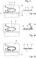
Fig. 1 schematische Draufsichten auf unterschiedliche Ausführungsformen von miteinander verbundenen Elementen einer erfindungsgemäßen Leiterplatte unter Verwendung des erfindungsgemäßen Verfahrens, wobei inFig. 1a ein Element einer Leiterplatte ein weiteres Element teilweise umgreift, bei der Ausführungsform gemäß -
Fig. 1b ein Element einer Leiterplatte vollständig von einem weiteren Element umgriffen ist, bei der Ausführungsform gemäßFig. 1c mehrere Leiterplattenelemente von einem gemeinsamen Element umgriffen bzw. umgeben sind und bei der Ausführungsform gemäßFig. 1d mehrere Leiterplattenelemente an einander gegenüberliegenden Rändern bzw. Kanten mit jeweils einem Rahmen- bzw. Trägerelement verbunden sind bzw. werden; -
Fig. 2 in vergrößertem Maßstab schematische Ansichten von unterschiedlichen Ausbildungen von Kopplungselementen zwischen miteinander zu verbindenden Elementen einer Leiterplatte; -
Fig. 3 schematisch den Verfahrensablauf einer Verbindung von miteinander zu verbindenden Elementen einer Leiterplatte, wobei inFig. 3a die Anordnung von miteinander zu verbindenden Elementen nebeneinander, inFig. 3b das Aufbringen eines Klebers zur Verbindung der miteinander zu verbindenden Elemente und inFig. 3c der Zustand dargestellt ist, nachdem der Kleber aufgetragen wurde; -
Fig. 4 in einer schematischen Draufsicht die relative Anordnung einer Mehrzahl von Elementen einer Leiterplatte zueinander unter Bezugnahme auf wenigstens ein Ausricht- bzw. Registrierelement; -
Fig. 5 eine schematische Draufsicht auf ein Trägerelement zur Anordnung einer Mehrzahl von miteinander zu verbindenden Elementen einer Leiterplatte, wobei zur provisorischen Festlegung ein Unterdruck bzw. Vakuum erzeugt bzw. angelegt wird; -
Fig. 6 eine schematische Darstellung einer abgewandelten Ausführungsform einer Anordnung einer Mehrzahl von Elementen auf einem Trägerelement, wobeiFig. 6a einen schematischen teilweisen Schnitt darstellt undFig. 6b eine schematische Draufsicht zeigt; -
Fig. 7 eine schematische Ansicht einer Ausbildung einer provisorischen Festlegung von zwei miteinander zu verbindenden Elementen unter Verwendung eines Klebestreifens; und -
Fig. 8 schematisch den Verfahrensablauf einer Verbindung und nachfolgenden Trennung von zwei Elementen beispielsweise zu Reparaturzwecken und für einen Ersatz von einem von derart miteinander verbundenen Elementen.
-
Fig. 1 schematic plan views of different embodiments of interconnected elements of a circuit board according to the invention using the method according to the invention, wherein inFig. 1a an element of a printed circuit board partially surrounds a further element, in the embodiment according to FIG -
Fig. 1b an element of a printed circuit board is completely encompassed by a further element, according to the embodiment according to FIGFig. 1c a plurality of circuit board elements are encompassed by a common element and in the embodiment according toFig. 1d a plurality of circuit board elements at opposite edges or edges are connected to a respective frame or support element or are; -
Fig. 2 on an enlarged scale schematic views of different configurations of coupling elements between elements to be connected to a circuit board; -
Fig. 3 schematically the process flow of a compound of interconnected elements of a printed circuit board, wherein inFig. 3a the arrangement of elements to be connected next to each other, inFig. 3b the application of an adhesive for connecting the elements to be joined together and inFig. 3c the condition is shown after the adhesive has been applied; -
Fig. 4 in a schematic plan view, the relative arrangement of a plurality of elements of a circuit board to each other with respect to at least one registration element; -
Fig. 5 a schematic plan view of a support member for arranging a plurality of interconnected elements of a printed circuit board, wherein for provisional determination, a vacuum or vacuum is created or applied; -
Fig. 6 a schematic representation of a modified embodiment of an arrangement of a plurality of elements on a support element, whereinFig. 6a represents a schematic partial section andFig. 6b shows a schematic plan view; -
Fig. 7 a schematic view of an embodiment of a provisional determination of two elements to be joined together using an adhesive strip; and -
Fig. 8 schematically the procedure of a compound and subsequent separation of two elements, for example, for repair purposes and for a replacement of one of such interconnected elements.
Zu den Figuren wird einleitend angemerkt, daß teilweise lediglich ein Teilbereich von Elementen einer herzustellenden Leiterplatte im Bereich einer Festlegung von aneinander festzulegenden bzw. miteinander zu verbindenden Elementen dargestellt ist. Weiters sind die gegenseitigen Abmessungen insbesondere im Hinblick auf einen zwischen den einzelnen Elementen vorzusehenden Abstand nicht maßstabsgemäß dargestellt. Darüber hinaus ist zur Vereinfachung der Darstellung auf den einzelnen Elementen einer herzustellenden Leiterplatte keinerlei Strukturierung angedeutet und es sind keinerlei gegebenenfalls festgelegte bzw. aufzunehmende Bauteile dargestellt.With regard to the figures, it will initially be noted that in some cases only a subarea of elements of a printed circuit board to be produced is shown in the region of a definition of elements to be fixed to one another or to be connected to one another. Furthermore, the mutual dimensions are not shown to scale, in particular with regard to a distance to be provided between the individual elements. In addition, to simplify the presentation on the individual elements of a printed circuit board to be produced no structuring is indicated and there are no optionally specified or male components shown.
In der Darstellung gemäß
Bei der Ausführungsform gemäß
Bei der Ausführungsform gemäß
Bei der Ausführungsform gemäß
Die in den
Bei der Ausführungsform gemäß
In
Während bei der Darstellung gemäß
Darüber hinaus sind die in
Ein Verbindungsvorgang von zwei miteinander zu verbindenden Elementen wird in größerem Detail anhand der Darstellung von
Bei dem in
Der Abstand 3 wird derart gewählt, daß er eine maximale Breite von 500 µm, günstigerweise 200 µm aufweist, so daß mit großen Produktionstoleranzen die miteinander zu verbindenden Elemente, welche gegebenenfalls zusätzliche Kopplungselemente 8 und 9 aufweisen, hergestellt werden können. Eine Einhaltung eines derartigen Abstands von beispielsweise maximal 200 µm erlaubt darüber hinaus, wie dies insbesondere unter Bezugnahme auf
Nach dem Anordnen der miteinander zu verbindenden Elemente in einer räumlichen Nahebeziehung zueinander, wie dies in
Wie aus der Darstellung gemäß
Nach dem Aufbringen des Klebers, wie dies in
Zur Vereinfachung weiterer Verfahrensschritte wird darüber hinaus auch eine Anpassung des Ausdehnungskoeffizienten des Klebers 12 an denjenigen der daran anschließenden Elemente 6 bzw. 10 vorgenommen.In order to simplify further method steps, an adaptation of the expansion coefficient of the adhesive 12 to that of the
Anstelle des in
Bei der Darstellung gemäß
Durch ein derartiges Verfahren wird es beispielsweise möglich, insbesondere unter Erhöhung bzw. Verbesserung der Festigkeit einer Verbindung zwischen benachbarten Elementen 6 und 10 durch Unterstützung der Kopplungselemente 8 und 9 eine Belastbarkeit von beispielsweise 2 kg zur Verfügung zu stellen, wobei dies für eine weitere Verwendung bzw. Bearbeitung derartiger Leiterplatten ausreichend ist. Darüber hinaus wird gewährleistet, daß auch beispielsweise in nachfolgenden Be- bzw. Verarbeitungsschritten, wie beispielsweise Reflow- bzw. Lötprozessen, beispielsweise zum Fixieren von Bauelementen keine Veränderungen an der hergestellten mechanischen Verbindung zwischen den miteinander zu verbindenden Elementen 6 und 10 auftreten.Such a method makes it possible, for example, to provide a load-bearing capacity of, for example, 2 kg, in particular by increasing or improving the strength of a connection between
In
Bei der schematischen Darstellung gemäß
Um einen Durchtritt eines Klebers im Bereich der Verbindung der miteinander zu verbindenden Elemente und somit ein Anhaften an dem Trägerelement 20 zu verhindern, ist darüber hinaus in
Bei der Ausführungsform gemäß
In dem wiederum mit 3 bezeichneten Spalt zwischen den Elementen 6 bzw. 10 wird, wie dies im Zusammenhang mit vorangehenden Ausführungsformen beschrieben wurde, wiederum ein Kleber zur Verbindung der Elemente 6 und 10 eingebracht.In the gap between the
Bei der Darstellung gemäß
Anstelle und/oder zusätzlich zu dem in
Darüber hinaus oder alternativ kann für eine Sicherung einer Positionierung der miteinander zu verbindenden Elemente 6 bzw. 10 die zu den miteinander zu verbindenden Elementen 6 bzw. 10 gerichtete Oberfläche des Trägerelements 20 bzw. 30 aus einem rutschfesten Material, wie beispielsweise Silikon, Gummi oder dgl. gebildet sein oder mit einem derartigen Material beschichtet sein. Derart kann insbesondere ohne zusätzliches Vorsehen eines Anlegens eines Unterdrucks, wie dies in
Bei der Darstellung gemäß
Aufgrund des vorgesehenen Abstands bzw. Spalts 3 zwischen miteinander zu verbindenden Elemente einer Leiterplatte, welcher nicht nur eine Vereinfachung der Herstellung sowie eine Automatisierung beim Zusammenfügen und Verbinden derselben ermöglicht, wird es auch möglich, beispielsweise schadhafte und gegebenenfalls mit kostspieligen Bauteilen bestückte Elemente einer Leiterplatte insbesondere entlang der Verbindungsstelle bzw. -linie voneinander zu trennen und insbesondere kostspielige Elemente einer Leiterplatte entsprechend zu ersetzen.Due to the provided distance or
In
Ausgehend von zwei Leiterplattenelementen I und II gemäß
Nach einer in
Es lassen sich somit einfach und mit großen Bearbeitungstoleranzen herzustellende Elemente einer Leiterplatte sicher und zuverlässig und bei verringertem Arbeitsaufwand und insbesondere mit der Möglichkeit einer Automatisierung des Anordnungs- und Verbindungsvorgangs miteinander verbinden.It can thus be easily and with great machining tolerances manufactured elements of a circuit board safely and reliably and with reduced workload and in particular with the possibility of automation of the arrangement and connection process together.
Claims (22)
- A method for connecting a plurality of elements of a printed circuit board, comprising the steps of- providing with mutually matching contours the elements to be connected (1, 2, 4, 5, 6, 10, 15, 16, I, II, III) of a printed circuit board,- arranging with mutually complementary contours in a close spatial relationship on at least one peripheral region (7, 11, 28, 29) the elements to be connected (1, 2, 4, 5, 6, 10, 15, 16, I, II, III), while keeping a distance (3) between the mutually facing peripheral regions (7, 11, 28, 29), and- mechanically connecting by gluing the mutually facing peripheral regions (7, 11, 28, 29) over at least portions thereof, for connecting the elements to be connected (1, 2, 4, 5, 6, 10, 15, 16, I, II, III) of the printed circuit board, wherein the printed circuit board elements to be connected (6, 10) are arranged or supported on a carrier element (20, 30) for carrying out the connecting procedure, the printed circuit board elements to be connected (6, 10) are kept secured to the carrier element (20, 30) during the connecting procedure by applying a vacuum, by clamping, by elevations or pins (31) projecting from the carrier element (30) entering complementary recesses (32) of the elements (6, 10), and/or the surface of the carrier element (20, 30) facing the elements (6, 10) to be supported is formed by, or coated with, an antiskid material, e.g. silicone, rubber or the like,characterized in that the distance (3) between the mutually facing peripheral regions to be connected (7, 11, 28, 29) is selected to be 500 µm at most and, in particular, 200 µm at most.
- A method according to claim 1, characterized in that elements to be connected (15, 16) are arranged and connected with reference to at least one aligning or registering element (17) provided on one of the elements to be connected.
- A method according to claim 1 or 2, characterized in that a thermally or chemically or UV or IR curable adhesive (12) is used for gluing.
- A method according to claim 3, characterized in that thermal curing of the adhesive (12) is carried out at temperatures between 80°C and 300°C.
- A method according to claim 4, characterized in that a high-viscosity adhesive (12) is used.
- A method according to any one of claims 1 to 5, characterized in that the adhesive (12) is applied by the aid of a dispensing device, template printing, screen printing or the like.
- A method according to any one of claims 3 to 6, characterized in that the adhesive (12) is merely introduced or arranged over a portion of the vertical extension of side edges of the peripheral regions to be connected (7, 11, 28, 29).
- A method according to any one of claims 1 to 7, characterized in that a temporary connection of peripheral regions to be connected (7, 11, 28, 29) is formed by using a removable adhesive tape or label (23).
- A method according to any one of claims 1 to 8, characterized in that a removable protective element (22), for instance a removable sheet of paper, is arranged below the peripheral regions to be connected, of the elements to be connected (6, 10).
- A method according to any one of claims 1 to 9, characterized in that connected elements (I, II, III) of a printed circuit board can be separated along the interconnected peripheral regions, e.g. for repair purposes, particularly by using a cutter or laser.
- A method according to any one of claims 1 to 10, characterized in that elements to be connected (6, 10), in a manner known per se, are each formed with at least one relatively complementary coupling element (8, 9) on peripheral regions to be connected (7, 11).
- A method according to claim 11, characterized in that the at least one coupling element (8) of an element (6) to be connected is formed by a profiled coupling element projecting from the peripheral region of said element and received in a complementary recess (9) of the element (10) to be connected therewith, while keeping said distance (3).
- A method according to claim 11 or 12, characterized in that a substantially rectangular element (6) of a printed circuit board, on respectively opposite peripheral regions, is each provided with at least one coupling element (8) each connected with a coupling element (9) of a frame or carrier element (10) cooperating therewith.
- A method according to claim 11, 12 or 13, characterized in that a plurality of elements (1, 2, 4, 5, 6, 10, 15, 16, I, II, III) of a printed circuit board are connected with one another in a spaced-apart relationship.
- A printed circuit board comprised of a plurality of interconnected elements, wherein at least two elements to be connected (1, 2, 4, 5, 6, 10, 15, 16, I, II, III) of the printed circuit board are mechanically connected by gluing with one another on at least one peripheral region (7, 11, 28, 29) thereof, while keeping a distance (3) and being supported on a carrier element,
characterized in that the distance (3) between the mutually facing peripheral regions to be connected (7, 11, 28, 29) is selected to be 500 µm at most and, in particular, 200 µm at most. - A printed circuit board according to claim 15, characterized in that elements to be connected (15, 16) are arranged, and connected with one another, with reference to at least one aligning or registering element (17) provided on one of the elements to be connected.
- A printed circuit board according to claim 15 or 16, characterized in that a thermally or chemically or UV or IR curable adhesive (12) is used for gluing.
- A printed circuit board according to claim 17, characterized in that the adhesive (12) is merely introduced or arranged over a portion of the vertical extension of side edges of the peripheral regions to be connected (7, 11, 28, 29).
- A printed circuit board according to any one of claims 15 to 18, characterized in that connected elements (I, II, III) of a printed circuit board are separable along the interconnected peripheral regions, e.g. for repair purposes, particularly by using a cutter or laser.
- A printed circuit board according to any one of claims 15 to 19, characterized in that elements to be connected (6, 10), in a manner known per se, are each formed with at least one relatively complementary coupling element (8, 9) on peripheral regions to be connected (7, 11).
- A printed circuit board according to claim 20, characterized in that the at least one coupling element (8) of an element to be connected (6) is formed by a profiled coupling element projecting from the peripheral region (7) of said element and received in a complementary recess (9) of the element (10) to be connected therewith, while keeping said distance.
- The use of the method according to any one of claims 1 to 14 for the production of a multi-part circuit board.
Applications Claiming Priority (2)
| Application Number | Priority Date | Filing Date | Title |
|---|---|---|---|
| AT0055209U AT12320U1 (en) | 2009-09-03 | 2009-09-03 | METHOD FOR CONNECTING A MULTIPLE OF ELEMENTS OF A CONDUCTOR PLATE, PCB, AND USE OF SUCH A METHOD |
| PCT/AT2010/000316 WO2011026165A1 (en) | 2009-09-03 | 2010-09-01 | Method for connecting a plurality of elements of a circuit board, circuit board, and use of such a method |
Publications (2)
| Publication Number | Publication Date |
|---|---|
| EP2474209A1 EP2474209A1 (en) | 2012-07-11 |
| EP2474209B1 true EP2474209B1 (en) | 2018-10-31 |
Family
ID=43064794
Family Applications (1)
| Application Number | Title | Priority Date | Filing Date |
|---|---|---|---|
| EP10755076.6A Active EP2474209B1 (en) | 2009-09-03 | 2010-09-01 | Method for connecting a plurality of elements of a circuit board, circuit board, and use of such a method |
Country Status (7)
| Country | Link |
|---|---|
| US (2) | US8863375B2 (en) |
| EP (1) | EP2474209B1 (en) |
| JP (1) | JP2013504182A (en) |
| CN (1) | CN102656954B (en) |
| AT (1) | AT12320U1 (en) |
| TW (1) | TW201125451A (en) |
| WO (1) | WO2011026165A1 (en) |
Families Citing this family (9)
| Publication number | Priority date | Publication date | Assignee | Title |
|---|---|---|---|---|
| JP2013197455A (en) * | 2012-03-22 | 2013-09-30 | Bosch Corp | Methods for manufacturing and repairing printed circuit board |
| TWI461127B (en) * | 2012-12-25 | 2014-11-11 | Univ Nat Taipei Technology | Electronic device and fabrication method thereof |
| US9084362B2 (en) * | 2013-01-08 | 2015-07-14 | Nvidia Corporation | Reducing impedance of a printed circuit board through a square wave pattern of plated-through holes |
| CN203151864U (en) | 2013-03-05 | 2013-08-21 | 奥特斯(中国)有限公司 | Printed circuit board |
| AT514074B1 (en) * | 2013-04-02 | 2014-10-15 | Austria Tech & System Tech | Method for producing a printed circuit board element |
| JP6051410B2 (en) * | 2013-09-24 | 2016-12-27 | パナソニックIpマネジメント株式会社 | Component mounting equipment |
| DE102014008148B4 (en) * | 2014-05-23 | 2020-06-04 | Continental Automotive Gmbh | Process for manufacturing a printed circuit board and printed circuit board |
| US11033048B2 (en) | 2015-04-01 | 2021-06-15 | Philip Morris Products S.A. | Homogenized tobacco material and method of production of homogenized tobacco material |
| US11189610B2 (en) * | 2018-06-27 | 2021-11-30 | Advanced Semiconductor Engineering, Inc. | Substrate structure and manufacturing process |
Citations (1)
| Publication number | Priority date | Publication date | Assignee | Title |
|---|---|---|---|---|
| US20020152609A1 (en) * | 1999-02-23 | 2002-10-24 | Samsung Electro-Mechanics Co., Ltd. | Method and device for coupling PCB sheet |
Family Cites Families (22)
| Publication number | Priority date | Publication date | Assignee | Title |
|---|---|---|---|---|
| US4255003A (en) * | 1975-11-13 | 1981-03-10 | Tektronix, Inc. | Electrical connector |
| US4293175A (en) * | 1978-06-08 | 1981-10-06 | Cutchaw John M | Connector for integrated circuit packages |
| JPS61265219A (en) | 1985-05-20 | 1986-11-25 | Hitachi Electronics Eng Co Ltd | Positioning method of substrate |
| US4689103A (en) | 1985-11-18 | 1987-08-25 | E. I. Du Pont De Nemours And Company | Method of manufacturing injection molded printed circuit boards in a common planar array |
| EP0360971A3 (en) * | 1988-08-31 | 1991-07-17 | Mitsui Mining & Smelting Co., Ltd. | Mounting substrate and its production method, and printed wiring board having connector function and its connection method |
| US5044615A (en) | 1991-02-08 | 1991-09-03 | International Business Machines Corporation | Dual purpose work board holder |
| DE19600928A1 (en) | 1996-01-12 | 1997-07-24 | Ibm | Handling device for number of circuit cards |
| TW492114B (en) * | 2000-06-19 | 2002-06-21 | Advantest Corp | Method and apparatus for edge connection between elements of an integrated circuit |
| EP1940208A3 (en) * | 2001-03-26 | 2009-08-05 | Ibiden Co., Ltd. | Multi-piece substrate and method of manufacturing the substrate |
| DE10131945A1 (en) | 2001-07-02 | 2003-01-30 | Siemens Dematic Ag | Process for joint processing of printed circuit boards |
| US6817527B2 (en) * | 2002-06-28 | 2004-11-16 | Nokia Corporation | Carriers for printed circuit board marking |
| WO2004023859A1 (en) * | 2002-09-03 | 2004-03-18 | Pcb Plus, Inc. | Apparatus and method for replacing defective pcb of pcb panel |
| JP3751938B2 (en) * | 2002-12-09 | 2006-03-08 | 日東電工株式会社 | TAB tape carrier and method for manufacturing the same |
| US7413481B2 (en) * | 2003-09-26 | 2008-08-19 | Redmond Iii Frank E | Systems for and methods of circuit construction |
| TWM257001U (en) * | 2003-11-27 | 2005-02-11 | Optimum Care Int Tech Inc | Improved memory module |
| JP2005322878A (en) * | 2004-04-09 | 2005-11-17 | Dainippon Printing Co Ltd | Assembly panel and mounting unit sheet for printed wiring board, rigid flexible board, and method for manufacturing them |
| US20080144299A1 (en) * | 2004-07-15 | 2008-06-19 | Redmond Frank E | Systems for and methods of circuit construction |
| FI20070910A0 (en) | 2007-11-27 | 2007-11-27 | Kimmo Olavi Paananen | A method for panel board paneling |
| US8698004B2 (en) * | 2008-10-27 | 2014-04-15 | Ibiden Co., Ltd. | Multi-piece board and fabrication method thereof |
| US8119454B2 (en) * | 2008-12-08 | 2012-02-21 | Stmicroelectronics Asia Pacific Pte Ltd. | Manufacturing fan-out wafer level packaging |
| CN101971719B (en) * | 2009-06-04 | 2013-01-16 | 揖斐电株式会社 | Method for manufacturing multi-piece substrate, and multi-piece substrate |
| US8547702B2 (en) * | 2009-10-26 | 2013-10-01 | Ibiden Co., Ltd. | Multi-piece board and method for manufacturing the same |
-
2009
- 2009-09-03 AT AT0055209U patent/AT12320U1/en not_active IP Right Cessation
-
2010
- 2010-09-01 WO PCT/AT2010/000316 patent/WO2011026165A1/en active Application Filing
- 2010-09-01 CN CN201080039334.XA patent/CN102656954B/en active Active
- 2010-09-01 EP EP10755076.6A patent/EP2474209B1/en active Active
- 2010-09-01 JP JP2012527154A patent/JP2013504182A/en active Pending
- 2010-09-01 US US13/393,697 patent/US8863375B2/en not_active Expired - Fee Related
- 2010-09-03 TW TW099129817A patent/TW201125451A/en unknown
-
2014
- 2014-09-19 US US14/490,840 patent/US20150014021A1/en not_active Abandoned
Patent Citations (1)
| Publication number | Priority date | Publication date | Assignee | Title |
|---|---|---|---|---|
| US20020152609A1 (en) * | 1999-02-23 | 2002-10-24 | Samsung Electro-Mechanics Co., Ltd. | Method and device for coupling PCB sheet |
Also Published As
| Publication number | Publication date |
|---|---|
| CN102656954B (en) | 2016-09-07 |
| EP2474209A1 (en) | 2012-07-11 |
| TW201125451A (en) | 2011-07-16 |
| CN102656954A (en) | 2012-09-05 |
| WO2011026165A1 (en) | 2011-03-10 |
| AT12320U1 (en) | 2012-03-15 |
| US8863375B2 (en) | 2014-10-21 |
| US20120160555A1 (en) | 2012-06-28 |
| US20150014021A1 (en) | 2015-01-15 |
| JP2013504182A (en) | 2013-02-04 |
Similar Documents
| Publication | Publication Date | Title |
|---|---|---|
| EP2474209B1 (en) | Method for connecting a plurality of elements of a circuit board, circuit board, and use of such a method | |
| EP2259311B1 (en) | Method for embedding at least one component into a circuit board element | |
| DE2920012B1 (en) | ID card with IC module and method for producing such an ID card | |
| EP2407014B1 (en) | Method and system for connecting a plurality of printed circuit boards to at least one frame or carrier element | |
| EP3026702B1 (en) | Method of producing a semiconductor element with substrate adapter and semiconductor element with substrate adapter | |
| WO2017125385A1 (en) | Method for attaching marking labels to a plurality of electrical devices which can be arranged on a support rail | |
| EP3940758A2 (en) | Method for connecting a substrate arrangement with an electronic component by sintering using a pre-fixing agent on a sintering contact material layer, corresponding substrate arrangement and method of manufacturing thereof | |
| EP1550358B1 (en) | Printed board comprising at least one stiff area and at least one flexible area, and method for the production of stiff-flexible printed boards | |
| DE10145749A1 (en) | Process for producing a structured metal layer on a carrier body and carrier body with a structured metal layer | |
| DE102010015408B4 (en) | Hot melt adhesive unit of a glue assembly | |
| EP2789214B1 (en) | Method for the production of a circuit board involving the removal of a subregion thereof, and use of such a method | |
| AT12738U1 (en) | METHOD AND SYSTEM FOR PROVIDING AN IN PARTICULAR A MULTIPLE OF LADDER PLATE ELEMENTS CONTAINING PLATE-SHAPED OBJECTS | |
| EP2982226B1 (en) | Method for producing a circuit board element | |
| DE20221189U1 (en) | Printed circuit board with at least one rigid area and at least one flexible area | |
| EP0126856A2 (en) | Method of making a circuit board having rigid and flexible areas | |
| EP2768290A1 (en) | Electronic component | |
| WO2016005146A1 (en) | Method for producing a substrate adapter, substrate adapter, and method for contacting a semiconductor element | |
| DE102005027276B3 (en) | Production process for a stack of at least two base materials comprising printed circuit boards photostructures the boards applies solder stacks and melts with lacquer separating the boards | |
| DE19819054B4 (en) | Method and device for mounting and adjusting components on a mounting base | |
| EP3120676A1 (en) | Electronic control module and method for producing the same | |
| EP2692215B1 (en) | Method for producing more particularly processing or populating, a circuit board element and carrier for use in such a method | |
| AT12722U1 (en) | PROCESS AND ASSOCIATION FOR EDITING OR BZW. TREATING A MULTIPLE OF PCBS AND USING HIEFÜR | |
| DE10258090B4 (en) | Method for producing rigid-flexible printed circuit boards and printed circuit boards with at least one rigid area and at least one flexible area | |
| EP3476574B1 (en) | Method for aligning and gluing two components using a two-component adhesive and device | |
| DE102018125645B3 (en) | Process for producing a tube lamp and corresponding tube lamp |
Legal Events
| Date | Code | Title | Description |
|---|---|---|---|
| PUAI | Public reference made under article 153(3) epc to a published international application that has entered the european phase |
Free format text: ORIGINAL CODE: 0009012 |
|
| 17P | Request for examination filed |
Effective date: 20120327 |
|
| AK | Designated contracting states |
Kind code of ref document: A1 Designated state(s): AL AT BE BG CH CY CZ DE DK EE ES FI FR GB GR HR HU IE IS IT LI LT LU LV MC MK MT NL NO PL PT RO SE SI SK SM TR |
|
| DAX | Request for extension of the european patent (deleted) | ||
| TPAC | Observations filed by third parties |
Free format text: ORIGINAL CODE: EPIDOSNTIPA |
|
| 17Q | First examination report despatched |
Effective date: 20141201 |
|
| GRAP | Despatch of communication of intention to grant a patent |
Free format text: ORIGINAL CODE: EPIDOSNIGR1 |
|
| STAA | Information on the status of an ep patent application or granted ep patent |
Free format text: STATUS: GRANT OF PATENT IS INTENDED |
|
| INTG | Intention to grant announced |
Effective date: 20180409 |
|
| GRAS | Grant fee paid |
Free format text: ORIGINAL CODE: EPIDOSNIGR3 |
|
| GRAJ | Information related to disapproval of communication of intention to grant by the applicant or resumption of examination proceedings by the epo deleted |
Free format text: ORIGINAL CODE: EPIDOSDIGR1 |
|
| GRAL | Information related to payment of fee for publishing/printing deleted |
Free format text: ORIGINAL CODE: EPIDOSDIGR3 |
|
| STAA | Information on the status of an ep patent application or granted ep patent |
Free format text: STATUS: EXAMINATION IS IN PROGRESS |
|
| GRAR | Information related to intention to grant a patent recorded |
Free format text: ORIGINAL CODE: EPIDOSNIGR71 |
|
| STAA | Information on the status of an ep patent application or granted ep patent |
Free format text: STATUS: GRANT OF PATENT IS INTENDED |
|
| INTC | Intention to grant announced (deleted) | ||
| GRAA | (expected) grant |
Free format text: ORIGINAL CODE: 0009210 |
|
| STAA | Information on the status of an ep patent application or granted ep patent |
Free format text: STATUS: THE PATENT HAS BEEN GRANTED |
|
| INTG | Intention to grant announced |
Effective date: 20180906 |
|
| AK | Designated contracting states |
Kind code of ref document: B1 Designated state(s): AL AT BE BG CH CY CZ DE DK EE ES FI FR GB GR HR HU IE IS IT LI LT LU LV MC MK MT NL NO PL PT RO SE SI SK SM TR |
|
| REG | Reference to a national code |
Ref country code: CH Ref legal event code: EP Ref country code: GB Ref legal event code: FG4D Free format text: NOT ENGLISH |
|
| REG | Reference to a national code |
Ref country code: AT Ref legal event code: REF Ref document number: 1060964 Country of ref document: AT Kind code of ref document: T Effective date: 20181115 |
|
| REG | Reference to a national code |
Ref country code: DE Ref legal event code: R096 Ref document number: 502010015522 Country of ref document: DE |
|
| REG | Reference to a national code |
Ref country code: IE Ref legal event code: FG4D Free format text: LANGUAGE OF EP DOCUMENT: GERMAN |
|
| REG | Reference to a national code |
Ref country code: NL Ref legal event code: MP Effective date: 20181031 |
|
| REG | Reference to a national code |
Ref country code: LT Ref legal event code: MG4D |
|
| PG25 | Lapsed in a contracting state [announced via postgrant information from national office to epo] |
Ref country code: HR Free format text: LAPSE BECAUSE OF FAILURE TO SUBMIT A TRANSLATION OF THE DESCRIPTION OR TO PAY THE FEE WITHIN THE PRESCRIBED TIME-LIMIT Effective date: 20181031 Ref country code: LT Free format text: LAPSE BECAUSE OF FAILURE TO SUBMIT A TRANSLATION OF THE DESCRIPTION OR TO PAY THE FEE WITHIN THE PRESCRIBED TIME-LIMIT Effective date: 20181031 Ref country code: IS Free format text: LAPSE BECAUSE OF FAILURE TO SUBMIT A TRANSLATION OF THE DESCRIPTION OR TO PAY THE FEE WITHIN THE PRESCRIBED TIME-LIMIT Effective date: 20190228 Ref country code: PL Free format text: LAPSE BECAUSE OF FAILURE TO SUBMIT A TRANSLATION OF THE DESCRIPTION OR TO PAY THE FEE WITHIN THE PRESCRIBED TIME-LIMIT Effective date: 20181031 Ref country code: BG Free format text: LAPSE BECAUSE OF FAILURE TO SUBMIT A TRANSLATION OF THE DESCRIPTION OR TO PAY THE FEE WITHIN THE PRESCRIBED TIME-LIMIT Effective date: 20190131 Ref country code: FI Free format text: LAPSE BECAUSE OF FAILURE TO SUBMIT A TRANSLATION OF THE DESCRIPTION OR TO PAY THE FEE WITHIN THE PRESCRIBED TIME-LIMIT Effective date: 20181031 Ref country code: LV Free format text: LAPSE BECAUSE OF FAILURE TO SUBMIT A TRANSLATION OF THE DESCRIPTION OR TO PAY THE FEE WITHIN THE PRESCRIBED TIME-LIMIT Effective date: 20181031 Ref country code: ES Free format text: LAPSE BECAUSE OF FAILURE TO SUBMIT A TRANSLATION OF THE DESCRIPTION OR TO PAY THE FEE WITHIN THE PRESCRIBED TIME-LIMIT Effective date: 20181031 Ref country code: NO Free format text: LAPSE BECAUSE OF FAILURE TO SUBMIT A TRANSLATION OF THE DESCRIPTION OR TO PAY THE FEE WITHIN THE PRESCRIBED TIME-LIMIT Effective date: 20190131 |
|
| PG25 | Lapsed in a contracting state [announced via postgrant information from national office to epo] |
Ref country code: PT Free format text: LAPSE BECAUSE OF FAILURE TO SUBMIT A TRANSLATION OF THE DESCRIPTION OR TO PAY THE FEE WITHIN THE PRESCRIBED TIME-LIMIT Effective date: 20190301 Ref country code: NL Free format text: LAPSE BECAUSE OF FAILURE TO SUBMIT A TRANSLATION OF THE DESCRIPTION OR TO PAY THE FEE WITHIN THE PRESCRIBED TIME-LIMIT Effective date: 20181031 Ref country code: AL Free format text: LAPSE BECAUSE OF FAILURE TO SUBMIT A TRANSLATION OF THE DESCRIPTION OR TO PAY THE FEE WITHIN THE PRESCRIBED TIME-LIMIT Effective date: 20181031 Ref country code: GR Free format text: LAPSE BECAUSE OF FAILURE TO SUBMIT A TRANSLATION OF THE DESCRIPTION OR TO PAY THE FEE WITHIN THE PRESCRIBED TIME-LIMIT Effective date: 20190201 Ref country code: SE Free format text: LAPSE BECAUSE OF FAILURE TO SUBMIT A TRANSLATION OF THE DESCRIPTION OR TO PAY THE FEE WITHIN THE PRESCRIBED TIME-LIMIT Effective date: 20181031 |
|
| PG25 | Lapsed in a contracting state [announced via postgrant information from national office to epo] |
Ref country code: DK Free format text: LAPSE BECAUSE OF FAILURE TO SUBMIT A TRANSLATION OF THE DESCRIPTION OR TO PAY THE FEE WITHIN THE PRESCRIBED TIME-LIMIT Effective date: 20181031 Ref country code: CZ Free format text: LAPSE BECAUSE OF FAILURE TO SUBMIT A TRANSLATION OF THE DESCRIPTION OR TO PAY THE FEE WITHIN THE PRESCRIBED TIME-LIMIT Effective date: 20181031 Ref country code: IT Free format text: LAPSE BECAUSE OF FAILURE TO SUBMIT A TRANSLATION OF THE DESCRIPTION OR TO PAY THE FEE WITHIN THE PRESCRIBED TIME-LIMIT Effective date: 20181031 |
|
| REG | Reference to a national code |
Ref country code: DE Ref legal event code: R097 Ref document number: 502010015522 Country of ref document: DE |
|
| PG25 | Lapsed in a contracting state [announced via postgrant information from national office to epo] |
Ref country code: SK Free format text: LAPSE BECAUSE OF FAILURE TO SUBMIT A TRANSLATION OF THE DESCRIPTION OR TO PAY THE FEE WITHIN THE PRESCRIBED TIME-LIMIT Effective date: 20181031 Ref country code: EE Free format text: LAPSE BECAUSE OF FAILURE TO SUBMIT A TRANSLATION OF THE DESCRIPTION OR TO PAY THE FEE WITHIN THE PRESCRIBED TIME-LIMIT Effective date: 20181031 Ref country code: SM Free format text: LAPSE BECAUSE OF FAILURE TO SUBMIT A TRANSLATION OF THE DESCRIPTION OR TO PAY THE FEE WITHIN THE PRESCRIBED TIME-LIMIT Effective date: 20181031 Ref country code: RO Free format text: LAPSE BECAUSE OF FAILURE TO SUBMIT A TRANSLATION OF THE DESCRIPTION OR TO PAY THE FEE WITHIN THE PRESCRIBED TIME-LIMIT Effective date: 20181031 |
|
| PLBE | No opposition filed within time limit |
Free format text: ORIGINAL CODE: 0009261 |
|
| STAA | Information on the status of an ep patent application or granted ep patent |
Free format text: STATUS: NO OPPOSITION FILED WITHIN TIME LIMIT |
|
| 26N | No opposition filed |
Effective date: 20190801 |
|
| PG25 | Lapsed in a contracting state [announced via postgrant information from national office to epo] |
Ref country code: SI Free format text: LAPSE BECAUSE OF FAILURE TO SUBMIT A TRANSLATION OF THE DESCRIPTION OR TO PAY THE FEE WITHIN THE PRESCRIBED TIME-LIMIT Effective date: 20181031 |
|
| PG25 | Lapsed in a contracting state [announced via postgrant information from national office to epo] |
Ref country code: TR Free format text: LAPSE BECAUSE OF FAILURE TO SUBMIT A TRANSLATION OF THE DESCRIPTION OR TO PAY THE FEE WITHIN THE PRESCRIBED TIME-LIMIT Effective date: 20181031 |
|
| PG25 | Lapsed in a contracting state [announced via postgrant information from national office to epo] |
Ref country code: MC Free format text: LAPSE BECAUSE OF FAILURE TO SUBMIT A TRANSLATION OF THE DESCRIPTION OR TO PAY THE FEE WITHIN THE PRESCRIBED TIME-LIMIT Effective date: 20181031 |
|
| REG | Reference to a national code |
Ref country code: CH Ref legal event code: PL |
|
| PG25 | Lapsed in a contracting state [announced via postgrant information from national office to epo] |
Ref country code: LU Free format text: LAPSE BECAUSE OF NON-PAYMENT OF DUE FEES Effective date: 20190901 Ref country code: LI Free format text: LAPSE BECAUSE OF NON-PAYMENT OF DUE FEES Effective date: 20190930 Ref country code: CH Free format text: LAPSE BECAUSE OF NON-PAYMENT OF DUE FEES Effective date: 20190930 Ref country code: IE Free format text: LAPSE BECAUSE OF NON-PAYMENT OF DUE FEES Effective date: 20190901 |
|
| REG | Reference to a national code |
Ref country code: BE Ref legal event code: MM Effective date: 20190930 |
|
| PG25 | Lapsed in a contracting state [announced via postgrant information from national office to epo] |
Ref country code: BE Free format text: LAPSE BECAUSE OF NON-PAYMENT OF DUE FEES Effective date: 20190930 |
|
| GBPC | Gb: european patent ceased through non-payment of renewal fee |
Effective date: 20190901 |
|
| PG25 | Lapsed in a contracting state [announced via postgrant information from national office to epo] |
Ref country code: GB Free format text: LAPSE BECAUSE OF NON-PAYMENT OF DUE FEES Effective date: 20190901 |
|
| REG | Reference to a national code |
Ref country code: AT Ref legal event code: MM01 Ref document number: 1060964 Country of ref document: AT Kind code of ref document: T Effective date: 20190901 |
|
| PG25 | Lapsed in a contracting state [announced via postgrant information from national office to epo] |
Ref country code: AT Free format text: LAPSE BECAUSE OF NON-PAYMENT OF DUE FEES Effective date: 20190901 |
|
| PG25 | Lapsed in a contracting state [announced via postgrant information from national office to epo] |
Ref country code: CY Free format text: LAPSE BECAUSE OF FAILURE TO SUBMIT A TRANSLATION OF THE DESCRIPTION OR TO PAY THE FEE WITHIN THE PRESCRIBED TIME-LIMIT Effective date: 20181031 |
|
| PG25 | Lapsed in a contracting state [announced via postgrant information from national office to epo] |
Ref country code: MT Free format text: LAPSE BECAUSE OF FAILURE TO SUBMIT A TRANSLATION OF THE DESCRIPTION OR TO PAY THE FEE WITHIN THE PRESCRIBED TIME-LIMIT Effective date: 20181031 Ref country code: HU Free format text: LAPSE BECAUSE OF FAILURE TO SUBMIT A TRANSLATION OF THE DESCRIPTION OR TO PAY THE FEE WITHIN THE PRESCRIBED TIME-LIMIT; INVALID AB INITIO Effective date: 20100901 |
|
| PG25 | Lapsed in a contracting state [announced via postgrant information from national office to epo] |
Ref country code: MK Free format text: LAPSE BECAUSE OF FAILURE TO SUBMIT A TRANSLATION OF THE DESCRIPTION OR TO PAY THE FEE WITHIN THE PRESCRIBED TIME-LIMIT Effective date: 20181031 |
|
| P01 | Opt-out of the competence of the unified patent court (upc) registered |
Effective date: 20230526 |
|
| PGFP | Annual fee paid to national office [announced via postgrant information from national office to epo] |
Ref country code: FR Payment date: 20230810 Year of fee payment: 14 Ref country code: DE Payment date: 20230816 Year of fee payment: 14 |