US11894193B2 - Multilayer electronic component - Google Patents
Multilayer electronic component Download PDFInfo
- Publication number
- US11894193B2 US11894193B2 US17/512,076 US202117512076A US11894193B2 US 11894193 B2 US11894193 B2 US 11894193B2 US 202117512076 A US202117512076 A US 202117512076A US 11894193 B2 US11894193 B2 US 11894193B2
- Authority
- US
- United States
- Prior art keywords
- dielectric
- electronic component
- internal electrodes
- multilayer electronic
- dielectric layer
- Prior art date
- Legal status (The legal status is an assumption and is not a legal conclusion. Google has not performed a legal analysis and makes no representation as to the accuracy of the status listed.)
- Active, expires
Links
- 239000000919 ceramic Substances 0.000 claims description 51
- 239000011230 binding agent Substances 0.000 claims description 41
- 239000000463 material Substances 0.000 claims description 29
- 239000003989 dielectric material Substances 0.000 claims description 26
- 238000000034 method Methods 0.000 claims description 22
- 239000000203 mixture Substances 0.000 claims description 22
- 238000003475 lamination Methods 0.000 claims description 12
- 238000010030 laminating Methods 0.000 claims description 10
- 238000004519 manufacturing process Methods 0.000 claims description 3
- 238000010586 diagram Methods 0.000 description 17
- PXHVJJICTQNCMI-UHFFFAOYSA-N Nickel Chemical compound [Ni] PXHVJJICTQNCMI-UHFFFAOYSA-N 0.000 description 16
- 238000005245 sintering Methods 0.000 description 15
- 229910002113 barium titanate Inorganic materials 0.000 description 13
- 239000000843 powder Substances 0.000 description 9
- 239000003985 ceramic capacitor Substances 0.000 description 8
- 229910052751 metal Inorganic materials 0.000 description 8
- 239000002184 metal Substances 0.000 description 8
- JRPBQTZRNDNNOP-UHFFFAOYSA-N barium titanate Chemical compound [Ba+2].[Ba+2].[O-][Ti]([O-])([O-])[O-] JRPBQTZRNDNNOP-UHFFFAOYSA-N 0.000 description 6
- 229910010293 ceramic material Inorganic materials 0.000 description 5
- 239000002131 composite material Substances 0.000 description 5
- 239000010949 copper Substances 0.000 description 5
- 229910052759 nickel Inorganic materials 0.000 description 5
- 238000007747 plating Methods 0.000 description 5
- 238000011049 filling Methods 0.000 description 4
- 239000011734 sodium Substances 0.000 description 4
- 239000000654 additive Substances 0.000 description 3
- 239000002270 dispersing agent Substances 0.000 description 3
- 239000003960 organic solvent Substances 0.000 description 3
- 238000007639 printing Methods 0.000 description 3
- 239000000047 product Substances 0.000 description 3
- 239000011347 resin Substances 0.000 description 3
- 229920005989 resin Polymers 0.000 description 3
- 238000000926 separation method Methods 0.000 description 3
- 239000002002 slurry Substances 0.000 description 3
- VEALVRVVWBQVSL-UHFFFAOYSA-N strontium titanate Chemical compound [Sr+2].[O-][Ti]([O-])=O VEALVRVVWBQVSL-UHFFFAOYSA-N 0.000 description 3
- RYGMFSIKBFXOCR-UHFFFAOYSA-N Copper Chemical compound [Cu] RYGMFSIKBFXOCR-UHFFFAOYSA-N 0.000 description 2
- DGAQECJNVWCQMB-PUAWFVPOSA-M Ilexoside XXIX Chemical compound C[C@@H]1CC[C@@]2(CC[C@@]3(C(=CC[C@H]4[C@]3(CC[C@@H]5[C@@]4(CC[C@@H](C5(C)C)OS(=O)(=O)[O-])C)C)[C@@H]2[C@]1(C)O)C)C(=O)O[C@H]6[C@@H]([C@H]([C@@H]([C@H](O6)CO)O)O)O.[Na+] DGAQECJNVWCQMB-PUAWFVPOSA-M 0.000 description 2
- WHXSMMKQMYFTQS-UHFFFAOYSA-N Lithium Chemical compound [Li] WHXSMMKQMYFTQS-UHFFFAOYSA-N 0.000 description 2
- ATJFFYVFTNAWJD-UHFFFAOYSA-N Tin Chemical compound [Sn] ATJFFYVFTNAWJD-UHFFFAOYSA-N 0.000 description 2
- 239000000956 alloy Substances 0.000 description 2
- 229910045601 alloy Inorganic materials 0.000 description 2
- 230000008901 benefit Effects 0.000 description 2
- 239000003990 capacitor Substances 0.000 description 2
- 230000015556 catabolic process Effects 0.000 description 2
- 229910052802 copper Inorganic materials 0.000 description 2
- 238000006731 degradation reaction Methods 0.000 description 2
- 230000000694 effects Effects 0.000 description 2
- 238000007646 gravure printing Methods 0.000 description 2
- 229910052744 lithium Inorganic materials 0.000 description 2
- 238000005259 measurement Methods 0.000 description 2
- 238000002156 mixing Methods 0.000 description 2
- 230000003287 optical effect Effects 0.000 description 2
- 239000002245 particle Substances 0.000 description 2
- 230000002093 peripheral effect Effects 0.000 description 2
- 239000011148 porous material Substances 0.000 description 2
- 239000002994 raw material Substances 0.000 description 2
- 238000007650 screen-printing Methods 0.000 description 2
- 229910052708 sodium Inorganic materials 0.000 description 2
- 239000000126 substance Substances 0.000 description 2
- 238000012935 Averaging Methods 0.000 description 1
- 229910018054 Ni-Cu Inorganic materials 0.000 description 1
- 229910018481 Ni—Cu Inorganic materials 0.000 description 1
- 230000015572 biosynthetic process Effects 0.000 description 1
- 239000011248 coating agent Substances 0.000 description 1
- 238000000576 coating method Methods 0.000 description 1
- 230000003247 decreasing effect Effects 0.000 description 1
- 230000007547 defect Effects 0.000 description 1
- 238000000280 densification Methods 0.000 description 1
- 230000002542 deteriorative effect Effects 0.000 description 1
- 238000007606 doctor blade method Methods 0.000 description 1
- 230000005611 electricity Effects 0.000 description 1
- 239000002003 electrode paste Substances 0.000 description 1
- 239000012467 final product Substances 0.000 description 1
- 239000011521 glass Substances 0.000 description 1
- 239000004973 liquid crystal related substance Substances 0.000 description 1
- 239000007769 metal material Substances 0.000 description 1
- 238000012986 modification Methods 0.000 description 1
- 230000004048 modification Effects 0.000 description 1
- 229910000510 noble metal Inorganic materials 0.000 description 1
- 230000000704 physical effect Effects 0.000 description 1
- 229920000642 polymer Polymers 0.000 description 1
- 239000002904 solvent Substances 0.000 description 1
Images


Classifications
-
- H—ELECTRICITY
- H01—ELECTRIC ELEMENTS
- H01G—CAPACITORS; CAPACITORS, RECTIFIERS, DETECTORS, SWITCHING DEVICES OR LIGHT-SENSITIVE DEVICES, OF THE ELECTROLYTIC TYPE
- H01G4/00—Fixed capacitors; Processes of their manufacture
- H01G4/002—Details
- H01G4/018—Dielectrics
- H01G4/06—Solid dielectrics
- H01G4/08—Inorganic dielectrics
- H01G4/12—Ceramic dielectrics
- H01G4/1209—Ceramic dielectrics characterised by the ceramic dielectric material
- H01G4/1218—Ceramic dielectrics characterised by the ceramic dielectric material based on titanium oxides or titanates
- H01G4/1227—Ceramic dielectrics characterised by the ceramic dielectric material based on titanium oxides or titanates based on alkaline earth titanates
-
- H—ELECTRICITY
- H01—ELECTRIC ELEMENTS
- H01G—CAPACITORS; CAPACITORS, RECTIFIERS, DETECTORS, SWITCHING DEVICES OR LIGHT-SENSITIVE DEVICES, OF THE ELECTROLYTIC TYPE
- H01G4/00—Fixed capacitors; Processes of their manufacture
- H01G4/002—Details
- H01G4/005—Electrodes
- H01G4/008—Selection of materials
- H01G4/0085—Fried electrodes
-
- H—ELECTRICITY
- H01—ELECTRIC ELEMENTS
- H01G—CAPACITORS; CAPACITORS, RECTIFIERS, DETECTORS, SWITCHING DEVICES OR LIGHT-SENSITIVE DEVICES, OF THE ELECTROLYTIC TYPE
- H01G4/00—Fixed capacitors; Processes of their manufacture
- H01G4/002—Details
- H01G4/018—Dielectrics
- H01G4/06—Solid dielectrics
- H01G4/08—Inorganic dielectrics
- H01G4/12—Ceramic dielectrics
- H01G4/1209—Ceramic dielectrics characterised by the ceramic dielectric material
-
- H—ELECTRICITY
- H01—ELECTRIC ELEMENTS
- H01G—CAPACITORS; CAPACITORS, RECTIFIERS, DETECTORS, SWITCHING DEVICES OR LIGHT-SENSITIVE DEVICES, OF THE ELECTROLYTIC TYPE
- H01G4/00—Fixed capacitors; Processes of their manufacture
- H01G4/002—Details
- H01G4/224—Housing; Encapsulation
-
- H—ELECTRICITY
- H01—ELECTRIC ELEMENTS
- H01G—CAPACITORS; CAPACITORS, RECTIFIERS, DETECTORS, SWITCHING DEVICES OR LIGHT-SENSITIVE DEVICES, OF THE ELECTROLYTIC TYPE
- H01G4/00—Fixed capacitors; Processes of their manufacture
- H01G4/30—Stacked capacitors
-
- H—ELECTRICITY
- H01—ELECTRIC ELEMENTS
- H01G—CAPACITORS; CAPACITORS, RECTIFIERS, DETECTORS, SWITCHING DEVICES OR LIGHT-SENSITIVE DEVICES, OF THE ELECTROLYTIC TYPE
- H01G4/00—Fixed capacitors; Processes of their manufacture
- H01G4/002—Details
- H01G4/005—Electrodes
- H01G4/012—Form of non-self-supporting electrodes
-
- H—ELECTRICITY
- H01—ELECTRIC ELEMENTS
- H01G—CAPACITORS; CAPACITORS, RECTIFIERS, DETECTORS, SWITCHING DEVICES OR LIGHT-SENSITIVE DEVICES, OF THE ELECTROLYTIC TYPE
- H01G4/00—Fixed capacitors; Processes of their manufacture
- H01G4/002—Details
- H01G4/228—Terminals
- H01G4/232—Terminals electrically connecting two or more layers of a stacked or rolled capacitor
Definitions
- the present disclosure relates to a multilayer electronic component.
- a multilayer ceramic capacitor (MLCC), a multilayer electronic component may be a chip-type condenser mounted on the printed circuit boards of various electronic products such as an image display device like a liquid crystal display (LCD) or a plasma display panel (PDP), a computer, smartphones, mobile phones and the like, and may charge or discharge electricity.
- an image display device like a liquid crystal display (LCD) or a plasma display panel (PDP)
- PDP plasma display panel
- Such a multilayer ceramic capacitor may be used as a component of various electronic devices as a multilayer ceramic capacitor may have a small size and high capacity, and may be easily mounted. As components of electronic devices have been designed to have a reduced size, demand for miniaturization and high capacity in a multilayer ceramic capacitor have increased.
- a method of configuring an internal electrode and a dielectric layer to have a reduced thickness and laminating the internal electrodes and the dielectric layers in multiple layers may be used.
- a mismatch between the elements may occur such that reliability of the multilayer ceramic capacitor may be deteriorated.
- a dielectric sheet may be present in a margin or a cover portion in which the internal electrode is not disposed, such that a difference may occur in reduction or expansion in burn-out and sintering. Accordingly, deformations such as distortion may occur between the core and the margin or between the core and the cover portion due to non-uniform stress, which may lead to product defects such as cracks or breakage due to reverse connection of the multilayer ceramic capacitor.
- An aspect of the present disclosure is to provide a multilayer electronic component which may secure reliability by reducing a difference in reduction rates between an active portion and a margin and between an active portion and a cover on which an internal electrode is disposed.
- a multilayer electronic component includes a body including a plurality of first dielectric layers, an active portion in which internal electrodes are alternately disposed, and a cover portion disposed on the active portion in a first direction of the body, a direction in which the plurality of first dielectric layers are laminated, and including a second dielectric layer; and an external electrode disposed externally on the body and connected to one of the internal electrodes.
- the body includes a margin portion covering a side surface of the one of the internal electrodes other than a side surface connected to the external electrode and including a dielectric pattern having a porosity higher than that of one of the plurality of first dielectric layers.
- a method of manufacturing a multilayer electronic component includes preparing a plurality of first ceramic green sheets on which a plurality of internal electrode patterns are respectively formed; forming a dielectric material at least partially in a region other than the internal electrode patterns with respect to the plurality of first ceramic green sheets; forming a laminate body by laminating the plurality of first ceramic green sheets such that adjacent internal electrodes of the internal electrode patterns intersect each other in a lamination direction in which the plurality of first ceramic green sheets are laminated, and laminating a second ceramic green sheet in the lamination direction on the plurality of first ceramic green sheets; and preparing a body including an active portion including a first dielectric layer made of one of the plurality of first ceramic green sheets, an internal electrode made of one of the internal electrode patterns, and a dielectric pattern made of the dielectric material, and a cover portion including a second dielectric layer made of the second ceramic green sheet, by baking the laminate body.
- the dielectric pattern has a porosity higher than that of the first dielectric layer
- a multilayer electronic component includes a body including first dielectric layers and internal electrodes alternately disposed, and a cover portion disposed on the active portion in a first direction of the body, a direction in which the first dielectric layers and the internal electrodes are laminated, the cover portion including a second dielectric layer; and an external electrode disposed externally on the body and connected to one of the internal electrodes.
- the body includes a margin portion covering a side surface of the one of the internal electrodes other than a side surface connected to the external electrode, the margin portion including a dielectric pattern.
- An average size of dielectric grains of one of the first dielectric layers disposed in a region overlapping the one of the internal electrodes in the active portion and an average size of dielectric grains disposed in the margin portion have a deviation of 50 nm or less therebetween.
- a multilayer electronic component includes a body including first dielectric layers and internal electrodes alternately disposed, and a cover portion disposed on the active portion in a first direction of the body, a direction in which the first dielectric layers and the internal electrodes are laminated, the cover portion including a second dielectric layer; and an external electrode disposed externally on the body and connected to one of the internal electrodes.
- the body includes a margin portion covering a side surface of the one of the internal electrodes other than a side surface connected to the external electrode, the margin portion including a dielectric pattern.
- a difference between an average size of dielectric grains of one of the first dielectric layers disposed in a region overlapping the one of the internal electrodes in the active portion and an average size of dielectric grains disposed in the margin portion, with respect to the average size of dielectric grains disposed in the margin portion, is 15.6% or less.
- FIG. 1 is a perspective diagram illustrating a multilayer electronic component according to an example embodiment of the present disclosure
- FIG. 2 is a cross-sectional diagram taken along line I-I′ in FIG. 1 ;
- FIG. 3 is a cross-sectional diagram taken along line II-II′ in FIG. 1 ;
- FIG. 4 is an exploded perspective diagram illustrating a body in which a dielectric layer and an internal electrode are laminated according to an example embodiment of the present disclosure
- FIG. 5 is a plan diagram illustrating a modified example of the body in FIG. 4 on an X-Z plane
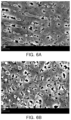
- FIGS. 6 A and 6 B are images of a boundary between an active portion and a margin portion of a multilayer electronic component according to an example embodiment of the present disclosure
- FIGS. 7 A and 7 B are images of a boundary between an active portion and a margin portion of a general multilayer electronic component
- FIG. 8 is an exploded perspective diagram illustrating a body in which a dielectric layer and an internal electrode are laminated according to an example embodiment of the present disclosure
- FIG. 9 is a cross-sectional diagram illustrating a modified example of a multilayer electronic component in FIG. 2 taken along line I-I′;
- FIG. 10 is a plan diagram illustrating a first internal electrode in FIG. 9 on an X-Y plane.
- X, Y, and Z in the drawings represent a length direction, a width direction, and a thickness direction of a multilayer electronic component, respectively.
- a length direction may be an X direction or a second direction
- a width direction may be a Y direction or a third direction
- the thickness direction may be a Z direction or a first direction.
- FIG. 1 is a perspective diagram illustrating a multilayer electronic component according to an example embodiment.
- FIG. 2 is a cross-sectional diagram taken along line I-I′ in FIG. 1 .
- FIG. 3 is a cross-sectional diagram taken along line II-II′ in FIG. 1 .
- FIG. 4 is an exploded perspective diagram illustrating a body in which a dielectric layer and an internal electrode are laminated according to an example embodiment.
- the multilayer electronic component 100 in an example embodiment may include a body 110 including a plurality of first dielectric layers 111 , and a plurality of internal electrodes 121 and 122 disposed with the first dielectric layer 111 interposed therebetween, and external electrodes 131 and 132 disposed externally on the body 110 and connected to the internal electrodes 121 and 122 .
- a shape of the body 110 is not limited to any particular shape, and may have a hexahedral shape or a shape similar to a hexahedron as illustrated in the diagram. Due to reduction of ceramic powder included in the body 110 during a baking process, the body 110 may have a substantially hexahedral shape.
- the body 110 may have first and second surfaces 1 and 2 opposing each other in the lamination direction (Z direction), third and fourth surfaces 3 and 4 connected to the first and second surfaces 1 and 2 and opposing each other in the length direction (X direction), and fifth and sixth surfaces 5 and 6 connected to the first to fourth surfaces 1 , 2 , 3 , and 4 and opposing each other in the width direction (Y direction).
- the body 110 may include an active portion in which the plurality of first dielectric layers 111 and the internal electrodes 121 and 122 are alternately disposed, and cover portions 112 and 113 disposed on both ends of the active portion in the first direction, the direction in which the first dielectric layers 111 are laminated, and including the second dielectric layer 116 .
- the active portion may contribute to formation of capacity of the capacitor, and may be formed by alternately disposing the plurality of internal electrodes 121 and 122 with the first dielectric layer 111 interposed therebetween.
- the plurality of first dielectric layers 111 included in the active portion may be in a baked state, and boundaries between the adjacent first dielectric layers 111 may be integrated such that it may be difficult to identify the boundaries without using a scanning electron microscope (SEM).
- SEM scanning electron microscope
- a raw material for forming the first dielectric layer 111 is not limited to any particular material as long as sufficient capacitance may be obtained.
- a barium titanate material, a lead composite perovskite material, a strontium titanate material, or the like may be used.
- a material for forming the first dielectric layers 111 may further include various ceramic additives, organic solvents, binders, and dispersants in addition to powder such as barium titanate (BaTiO 3 ).
- the cover portions 112 and 113 may include an upper cover portion 112 and a lower cover portion 113 , and may prevent damage to the internal electrodes caused by physical or chemical stress.
- the cover portions 112 and 113 may not include the internal electrodes.
- the cover portions 112 and 113 may be formed by laminating the second dielectric layers 116 above and below the active portion in the thickness direction.
- the plurality of second dielectric layers 116 included in the cover portions 112 and 113 may be in a baked state, and boundaries between the second dielectric layers 116 adjacent to each other may be integrated such that it may be difficult to identify the boundaries without using a scanning electron microscope (SEM).
- SEM scanning electron microscope
- a raw material for forming the second dielectric layer 116 is not limited to any particular material as long as sufficient capacitance may be obtained.
- a barium titanate material, a lead composite perovskite material, a strontium titanate material, or the like may be used.
- a material for forming the second dielectric layers 116 may further include various ceramic additives, organic solvents, binders, and dispersants in addition to powder such as barium titanate (BaTiO 3 ).
- the first dielectric layer 111 included in the active portion and the second dielectric layer 116 included in the cover portions 112 and 113 may have different dielectric compositions.
- the first dielectric layer 111 and the second dielectric layer 116 may be formed of different types of ceramic materials, or may include subcomponents such as lithium (Li) and sodium (Na) in different compositions.
- the first dielectric layer 111 included in the active portion and the second dielectric layer 116 included in the cover portions 112 and 113 may have the same dielectric composition. In this case, even though the dielectric compositions are the same, sizes of ceramic particles included in the first dielectric layer 111 and the second dielectric layer 116 may be different.
- a porosity of the first dielectric layer 111 included in the active portion may be different from a porosity of the second dielectric layer 116 included in the cover portions 112 and 113 . Accordingly, an average porosity of the first dielectric layer 111 and an average porosity of the cover portions 112 and 113 , included in the active portion, may be different from each other in the final product.
- the plurality of internal electrodes 121 and 122 may be alternately disposed with the plurality of first dielectric layers 111 interposed therebetween.
- the external electrodes 131 and 132 may be formed on both end surfaces of the body 110 in the second direction (X direction), and the plurality of internal electrodes 121 and 122 may include the first and second internal electrodes 121 and 122 connected to the external electrodes 131 and 132 , respectively.
- the first and second internal electrodes 121 and 122 may be alternately disposed to oppose each other with the first dielectric layer 111 forming the active portion of the body 110 interposed therebetween, and may be exposed to the fourth surfaces 3 and 4 of the body 110 , respectively.
- the first internal electrode 121 may be spaced apart from the fourth, fifth and sixth surfaces 4 , 5 , and 6 and may be exposed through the third surface 3
- the second internal electrode 122 may be spaced apart from the third, fifth, and sixth surfaces 3 , 5 , and 6 and may be exposed through the fourth surface 4 .
- the first external electrode 131 may be disposed on the third surface 3 of the body 110 and may be connected to the first internal electrode 121
- the second external electrode 132 may be disposed on the fourth surface 4 of the body and may be connected to the second internal electrode 122 .
- first external electrode 131 and the second internal electrode 122 may be spaced apart from each other in the second direction (X direction), the second external electrode 132 and the first internal electrode 121 may be spaced apart from each other in the second direction (X direction), and shortest spacings therebetween may be the same.
- the body 110 may be formed by alternately laminating the first dielectric layer 111 on which the first internal electrode 121 is printed and the first dielectric layer 111 on which the second internal electrode 122 is printed in the thickness direction (Z direction), and baking the dielectric layers.
- first and second internal electrodes 121 and 122 may be electrically separated from each other by the first dielectric layer 111 interposed therebetween.
- a material for forming the first and second internal electrodes 121 and 122 is not limited to any particular material, and may be formed using a conductive paste formed of at least one of a noble metal material or nickel (Ni) and copper (Cu).
- a screen-printing method or a gravure printing method may be used, and an example embodiment thereof is not limited thereto.
- a margin portion may be disposed on a side surface of the active portion of the body 110 .
- the margin portion may prevent damages to the internal electrode caused by physical or chemical stress.
- the margin portion may cover a side surface of the internal electrodes 121 and 122 other than a side surface connected to the external electrodes 131 and 132 .
- the margin portion may be formed by forming the internal electrode by applying a conductive paste on a region of the ceramic green sheet other than a portion in which the margin portion is formed.
- the internal electrodes 121 and 122 may include the first internal electrode 121 connected to the third surface 3 of the body 110 and spaced apart from the fourth, fifth and sixth surfaces 4 , 5 , and 6 , and the second internal electrode 122 connected to the fourth surface 4 of the body 110 and spaced apart from the third, fifth and sixth surfaces 3 , 5 and 6 .
- the internal electrodes may be connected to the external electrodes 131 and 132 through the third and fourth surfaces 3 and 4 , respectively.
- the margin portion may be disposed to cover the side surface adjacent to the fourth, fifth and sixth sides 4 , 5 , and 6 surfaces of the body 110 and the side surface adjacent to the third, fifth and sixth surfaces 3 , 5 , and 6 in the internal electrodes 121 and 122 .
- the margin portion may include the margin portion 114 disposed on the sixth surface 6 of the body 110 and the margin portion 115 disposed on the fifth surface 5 .
- the margin portion may include the margin portions 114 and 115 disposed on both side surfaces of the ceramic body 110 in the width direction.
- the margin portion may include dielectric patterns 141 and 142 .
- the internal electrodes 121 and 122 are disposed on the plurality of first dielectric layers 111 , respectively, and the margin portion may be formed in a region in which the internal electrodes 121 and 122 are not disposed, and the dielectric patterns 141 and 142 may be disposed in the margin portions, respectively.
- the dielectric patterns 141 and 142 may be disposed to fill a tolerance formed between the first dielectric layers 111 as the first and second internal electrodes 121 and 122 are alternately disposed, such that the dielectric patterns 141 and 142 may prevent cracks of or damages to the multilayer electronic component 100 .
- the dielectric patterns 141 and 142 may be disposed to fill a tolerance formed on the marginal portions 114 and 115 on both ends in the third direction (Y direction) in the active portion of the body 110 as illustrated in FIG. 3 , and accordingly, breakage caused by non-uniform reduction or expansion between the active portion and the margin portion in sintering the multilayer electronic component 100 may be prevented.
- the dielectric patterns 141 and 142 may include the first dielectric pattern 141 spaced apart from the fourth, fifth and sixth surfaces 4 , 5 , and 6 of the body 110 and disposed around the first internal electrode 121 , and the second dielectric pattern 142 spaced apart from the third, fifth and sixth surfaces 3 , 5 , and 6 of the body 110 and disposed around the second internal electrode 122 .
- the first dielectric pattern 141 may be disposed to fill a region of the first dielectric layer 111 in which the first internal electrode 121 is not formed
- the second dielectric pattern 142 may be disposed to fill a region of the first dielectric layer 111 in which the second internal electrode 122 is not formed.
- the dielectric patterns 141 and 142 may be formed of a dielectric material.
- the dielectric material for forming the dielectric patterns 141 and 142 is not limited to any particular material as long as sufficient capacitance may be obtained.
- a barium titanate material, a lead composite perovskite material, a strontium titanate material, or the like may be used.
- the material for forming the dielectric patterns 141 and 142 may further include various ceramic additives, organic solvents, binders, and dispersants in addition to powder such as barium titanate (BaTiO 3 ).
- the dielectric patterns 141 and 142 and the first dielectric layer 111 may have different porosities.
- a porosity of the dielectric patterns 141 and 142 may be higher than a porosity of the first dielectric layer 111 .
- a porosity of the dielectric patterns 141 and 142 and a porosity of the first dielectric layer 111 may be varied according to a difference in content of a binder included in each of the dielectric material and the ceramic green sheet applied in the process of forming the dielectric patterns 141 and 142 and the first dielectric layer 111 .
- the dielectric patterns 141 and 142 may have a relatively high porosity, and the first dielectric layer 111 may have a relatively low porosity.
- a greater amount of binder may be included in the dielectric material for forming the dielectric patterns 141 and 142 , such that the dielectric patterns 141 and 142 may have a reduction rate higher than that of the dielectric layer 111 .
- the reduction rate of the internal electrode may be generally lower than that of the dielectric layer, such that a deviation in the reduction rate may occur in the process of sintering the electronic component. Accordingly, deformation such as reverse connection may occur in the electronic component due to non-uniform reduction, which may be a factor deteriorating reliability.
- the dielectric patterns 141 and 142 in the example embodiment may have a reduction rate corresponding to a value between the reduction rate of the first dielectric layer 111 and the reduction rate of the internal electrodes 121 and 122 , such that degradation in reliability of the first dielectric layer 111 and the internal electrodes 121 and 122 caused by the deviation in the reduction rate may be prevented.
- the first dielectric layer 111 and the dielectric patterns 141 and 142 included in the active portion may have different dielectric compositions.
- the first dielectric layer 111 and the dielectric patterns 141 and 142 may be formed of different types of ceramic materials, or may include subcomponents such as lithium (Li) and sodium (Na) in different compositions.
- the first dielectric layer 111 and the dielectric patterns 141 and 142 may have the same dielectric composition other than the content of the binder before sintering.
- the dielectric compositions are the same, the sizes of ceramic particles included in the first dielectric layer 111 and the dielectric patterns 141 and 142 may be different.
- the dielectric composition of the dielectric patterns 141 and 142 and the dielectric composition of the second dielectric layer 116 may be the same.
- the dielectric patterns 141 and 142 formed in the margin portions and the cover portions 112 and 113 of the body 110 formed by the second dielectric layer 116 may have the same dielectric composition.
- the dielectric patterns 141 and 142 and the second dielectric layer 116 may have the same average porosity.
- the content of a binder included in the dielectric material forming the dielectric patterns 141 and 142 and the ceramic green sheet forming the second dielectric layer 116 may be the same. Accordingly, the reduction rates of the dielectric patterns 141 and 142 and the second dielectric layer 116 may be almost the same during sintering.
- the cover portions 112 and 113 may be configured to have the reduction rate similar to an average reduction rate of the active portion.
- the cover portions 112 and 113 may be configured to have a reduction rate similar to the average value of the reduction rate of the first dielectric layer 111 , the internal electrodes 121 and 122 , and the dielectric patterns 141 and 142 , included in the active portion, a deviation in reduction rates between the active portion and the cover portions 112 and 113 may be reduced.
- the external electrodes 131 and 132 may be disposed on the body 110 and may be connected to the internal electrodes 121 and 122 .
- the external electrodes 131 and 132 may include first and second external electrodes 131 and 132 disposed on the third and fourth surfaces 3 and 4 of the body 110 , respectively, and connected to the first and second internal electrodes 121 and 122 , respectively.
- the multilayer electronic component 100 has two external electrodes 131 and 132 is described, but the number or the shape of the external electrodes 131 and 132 may be varied depending on the shape of the internal electrodes 121 and 122 and other purposes.
- the external electrodes 131 and 132 may be formed using various materials having electrical conductivity such as metal, and a specific material may be determined in consideration of electrical properties and structural stability.
- the external electrodes 131 and 132 may be baked electrodes including conductive metal and glass, or resin electrodes including conductive metal and resin.
- the external electrodes 131 and 132 may have a shape in which a baked electrode and a resin electrode are formed in order on the body 110 . Also, the external electrodes 131 and 132 may be formed by transferring a sheet including a conductive metal to the body 110 or by transferring a sheet including a conductive metal to the sintered electrode.
- a material having excellent electrical conductivity may be used as the conductive metal included in the external electrodes 131 and 132 , and the material is not limited to any particular material.
- the conductive metal may be one or more of nickel (Ni), copper (Cu), and alloys thereof.
- first and second external electrodes 131 and 132 may further include a plating layer.
- the plating layer may include first and second nickel (Ni) plating layers, and first and second tin (Sn) plating layers covering the first and second nickel plating layers, respectively.
- FIG. 5 is a plan diagram illustrating a modified example of the body in FIG. 4 on an X-Z plane.
- a body 110 - 1 according to the modified example may include dielectric patterns 141 and 142 having a limited height.
- the first dielectric layer 111 and the internal electrodes 121 and 122 may be alternately disposed to form an active portion, similarly to the body 110 illustrated in FIG. 4 .
- the second dielectric layers 116 may be laminated on both ends in the lamination direction (first direction) to form the cover portions 112 and 113 .
- the dielectric patterns 141 and 142 may have a filling rate of 30% to 90% with respect to the margin portion.
- t 1 an average height of the dielectric patterns 141 and 142 in the first direction
- t 2 an average height of the internal electrodes 121 and 122 in the first direction
- t 1 may satisfy 0.3t 2 ⁇ t 1 ⁇ 0.9t 2 .
- the dielectric patterns 141 and 142 may be formed to have the same height as that of the internal electrodes 121 and 122 , and in this case, reverse connection or disconnection may occur due to reduction or expansion in sintering the multilayer electronic component. Therefore, preferably, the dielectric patterns 141 and 142 may be formed to have a height of 90% or less of the entire height of the margin portion in the first direction. In other words, an average height t 1 of the dielectric patterns 141 and 142 in the first direction may satisfy t 1 ⁇ 0.9t 2 .
- the filling rate of the margin portion may be low, such that the effect of filling the tolerance formed between the first dielectric layers 111 may not be properly obtained. Accordingly, non-uniform deformation such as reverse connection of the multilayer electronic component 100 may not be effectively prevented.
- the filling rate of the margin portion has a low value, less than 30%, withstand voltage properties (BDV) of the multilayer electronic component 100 may not reach a required value.
- the dielectric patterns 141 and 142 may be formed to have a height of 30% or more of the entire height of the margin portion in the first direction. Accordingly, the average height t 1 of the dielectric patterns 141 and 142 in the first direction may satisfy 0.3t 2 ⁇ t 1 .
- the average heights t 11 and t 12 of the second dielectric layer 116 forming the cover portion in the first direction are not limited to any particular example. As an example, as illustrated in FIG. 5 , the average heights t 11 and t 12 of the second dielectric layer 116 in the first direction may be the same as the average height t 1 of the dielectric patterns 141 and 142 in the first direction.
- the average height t 3 of the first dielectric layer 111 in the first direction is not limited to any particular example. As an example, as illustrated in FIG. 5 , the average height t 3 of the first dielectric layer 111 in the first direction may be greater than the average height t 1 of the dielectric patterns 141 and 142 in the first direction. Also, the average height t 3 of the first dielectric layer 111 in the first direction may be the same as the average height t 2 of the internal electrodes 121 and 122 in the first direction.
- the heights of the dielectric layers 111 and 116 in the first direction may be varied if desired.
- An average height of each element is an average value of the heights of the elements in the first direction from a plurality of cross-sectional surfaces (e.g., ten cross-sectional surfaces with the same spacing) of the multilayer electronic component in parallel to an X-Z plane or a Y-Z plane.
- an average height of each element is an average value of the heights of the element in the first direction measured at locations with the same spacing in the X direction of a cross-sectional surface of the multilayer electronic component in parallel to an X-Z plane, or is an average value of the heights of the element measured at locations with the same spacing at locations at the same spacing in the Y direction of a cross-sectional surface of the multilayer electronic component in parallel to a Y-Z plane.
- the measurement may be performed by an optical microscope or a scanning electron microscope (SEM), although the present disclosure is not limited thereto. Other parameters may be measured in a similar manner. Other methods and/or tools appreciated by one of ordinary skill in the art, even if not described in the present disclosure, may also be used.
- SEM scanning electron microscope
- the heights of the elements in the first direction with respect to the different cross-sectional surfaces thereof may be different.
- the dielectric patterns 141 and 142 , the first dielectric layers 111 , the second dielectric layers 116 , and the internal electrodes 121 and 122 may not have a constant height, and may be formed in a shape protruding or being recessed in partial regions.
- a plurality of first ceramic green sheets may be prepared.
- the first ceramic green sheet may be provided to form the first dielectric layer 111 of the body 110 , and may be formed by forming slurry by mixing ceramic powder, a polymer, and a solvent and forming the slurry in a sheet shape through method such as a doctor blade method.
- the ceramic powder included in the slurry forming the first dielectric layer may include BaTiO 3 as a main component.
- internal electrodes 121 and 122 may be formed by printing a conductive paste for internal electrodes on at least one surface of each of the first ceramic green sheets.
- the conductive paste for internal electrodes may be formed by mixing Ni powder and Cu powder or including Ni—Cu alloy powder, for example.
- a screen printing method or a gravure printing method may be used as the method of printing the conductive paste for internal electrodes.
- a dielectric material may be arranged in at least a portion of a region other than the first and second internal electrode patterns with respect to each of the plurality of first ceramic green sheets.
- the dielectric material may correspond to a material forming the dielectric patterns 141 and 142 , and the dielectric patterns 141 and 142 may have a porosity higher than that of the first dielectric layer 111 .
- a volume fraction of a binder included in the first ceramic green sheet is A
- a volume fraction of a binder included in the first and second internal electrode patterns is B
- a volume fraction of a binder included in the dielectric material is defined as C
- A, B, and C may satisfy A>C ⁇ B.
- a content of the binder of the dielectric material forming the dielectric patterns 141 and 142 may correspond to a value between the contents of the binders included in the first ceramic green sheet and the internal electrode pattern, or may be equal to the content of the binder of the internal electrode pattern.
- the reduction rate in sintering of the dielectric patterns 141 and 142 may correspond to a value between the reduction rates of the first dielectric layer 111 and the internal electrodes 121 and 122 , or may be almost the same as the reduction rate of the internal electrodes 121 and 122 . Accordingly, a porosity of the dielectric patterns 141 and 142 included in the margin portion may be higher than a porosity of the first dielectric layer 111 included in the active portion.
- the plurality of first ceramic green sheets may be alternately laminated such that the first internal electrode pattern and the second internal electrode pattern may intersect, and the plurality of first ceramic green sheets may be pressured in the lamination direction, such that the plurality of laminated first ceramic green sheets and the internal electrodes formed on the first ceramic green sheets may be compressed, thereby forming a laminate body.
- cover portions 112 and 113 may be formed by laminating at least one or more second ceramic green sheets above and below the laminate body.
- the cover portions 112 and 113 may have the same composition as that of the first dielectric layer 111 disposed in the laminate body, and may be different from the first dielectric layer 111 in that the cover portions 112 and 113 do not include the internal electrodes.
- the second ceramic green sheet may form a second dielectric layer 116 , and a dielectric composition of the second ceramic green sheet may be the same as the composition of the dielectric material forming the dielectric patterns 141 and 142 .
- the first ceramic green sheet and the second ceramic green sheet may include different contents of binders. Accordingly, a porosity of the first dielectric layer 111 included in the active portion may be different from a porosity of the cover portions 112 and 113 .
- the laminate body may be cut into chips for each region corresponding to a single capacitor, and may be baked at a high temperature, such that the body 110 including the active portion including the first dielectric layer 111 , the internal electrodes 121 and 122 , and the dielectric patterns 141 and 142 and the cover portions 112 and 113 including the second dielectric layer 116 may be manufactured.
- the first and second internal electrodes 121 and 122 may be formed to be electrically connected to the first and second internal electrodes 121 and 122 by covering the exposed portions of the first and second internal electrodes 121 and 122 , exposed to both side surfaces of the body 110 .
- surfaces of the first and second external electrodes 131 and 132 may be plated with nickel (Ni) or tin (Sn), if desired.
- FIGS. 6 A and 6 B are images of a boundary between an active portion and a margin portion of a multilayer electronic component according to an example embodiment.
- FIGS. 7 A and 7 B are images of a boundary between an active portion and a margin portion of a general multilayer electronic component.
- the left side is an active portion including an internal electrode
- the right side is a margin portion without an internal electrode
- the intermediate side is the end of the internal electrode, the boundary between the active portion and the margin portion.
- FIGS. 6 A to 7 B differently from the general multilayer electronic component illustrated in FIGS. 7 A and 7 B , a greater number of pores were observed in the image of the multilayer electronic component in the example embodiment illustrated in FIGS. 6 A and 6 B . Also, in FIGS. 6 A and 6 B , a greater number of pores were observed in the margin portion on the right side than in the active portion on the left side.
- the porosity appeared as above because a large amount of binder was included in the dielectric material forming the dielectric patterns 141 and 142 included in the margin portion in the forming the body 110 in the example embodiment.
- the dielectric patterns 141 and 142 of the margin portion and the first dielectric layer 111 of the active portion may have different porosities depending on the content of binders included in the dielectric material and the ceramic green sheet applied in the process of forming the dielectric patterns 141 and 142 of the margin portion and the first dielectric layer 111 of the active portion.
- a greater amount of binder may be included in the dielectric material forming the dielectric patterns 141 and 142 , such that the dielectric patterns 141 and 142 may have a relatively high porosity, and the first dielectric layer 111 may have a relatively low porosity.
- the multilayer electronic component 100 in the example embodiment may include a greater amount of binder in the dielectric material forming the dielectric patterns 141 and 142 , such that the dielectric patterns 141 and 142 may be configured to have a reduction rate higher than that of the dielectric layer 111 . Also, by reducing the deviation in the reduction rate occurring in the sintering the electronic component, reliability of the multilayer electronic component 100 may be secured.
- Table 1 below lists the reduction rates depending on the content of binder of the material for forming each element when the multilayer electronic component 100 in an example embodiment illustrated in FIG. 6 is manufactured.
- the reduction rates in Table 1 were obtained by calculating a value of a theoretical linear reduction rate.
- the theoretical linear reduction rate may refer to a reduction rate of when an object having a porosity a is isotropic-reduced in the X, Y, and Z directions and reaches full densification. Therefore, the theoretical linear reduction rate may refer to a linear reduction in one of the X, Y, and Z directions.
- a content of the binder included in the first dielectric layer represents a ratio of a volume of the binder to an entire volume of the first ceramic green sheet forming the first dielectric layer including the ceramic material such as BaTiO 3 before sintering.
- the content of the binder included in the internal electrode represents a ratio of a volume of the binder to an entire volume of the internal electrode paste forming the internal electrode pattern including a conductive metal such as Ni before sintering.
- the content of the binder included in the second dielectric layer represents a ratio of a volume of the binder to an entire volume of the second ceramic green sheet forming the second dielectric layer including a ceramic material such as BaTiO 3 before sintering.
- the content of the binder included in the dielectric pattern represents a ratio of a volume of the binder to an entire volume of the dielectric material forming the dielectric pattern including ceramic material such as BaTiO 3 before sintering.
- the content of the binder of the dielectric patterns 141 and 142 was determined to be a value between the contents of the binders of the first dielectric layer 111 and the internal electrodes 121 and 122 , thereby reducing the deviation in reduction rate between the first dielectric layer 111 and the internal electrodes 121 and 122 . Accordingly, the deviation in reduction rate between the active portion and the margin portion was decreased, and degradation of reliability caused by deformation or reverse connection of the multilayer electronic component 100 may be prevented.
- the reduction rates of the first dielectric layer 111 and the internal electrodes 121 and 122 may be almost the same, such that the same effect as in the above experimental example may be obtained.
- the volume fraction of the binder included in the first ceramic green sheet is defined as A
- the volume fraction of the binder included in the internal electrode pattern is defined as B
- the volume fraction of the binder included in the dielectric material is defined as C
- A, B, and C may satisfy A>C ⁇ B.
- the content of the binder of the second dielectric layer 116 forming the cover portions 112 and 113 may be determined to be a value between the contents of the binders of the first dielectric layer 111 and the internal electrodes 121 and 122 , the deviation in reduction rates between the active portion and the cover portions 112 and 113 may be reduced. Accordingly, separation of and damages to the cover portions 112 and 113 caused by non-uniform deformation of the multilayer electronic component 100 may be prevented.
- a deviation between an average size of dielectric grains included in the active portion and an average size of dielectric grains included in the margin portion may be relative low.
- a deviation between an average size of dielectric grains included in the active portion and an average size of dielectric grains included in the margin portion may be relative high.
- the average size of dielectric grains may be determined within a region selected by one of ordinary skill in the art and calculated by averaging the measured sizes of the dielectric grains within the selected region. The measurement may be performed by an optical microscope or a scanning electron microscope (SEM), although the present disclosure is not limited thereto. Other methods and/or tools appreciated by one of ordinary skill in the art, even if not described in the present disclosure, may also be used.
- the average size of the dielectric grains of the dielectric layer included in the active portion in FIG. 7 A was 0.28 ⁇ m, and the average size of the dielectric grains disposed in the margin portion was 0.42 ⁇ m.
- the average size of the dielectric grains of the dielectric layer included in the active portion was 0.32 ⁇ m, and the average size of the dielectric grains disposed in the margin portion was 0.42 ⁇ m.
- the average size of the dielectric layer included in the active portion and the dielectric grains of the margin portion were different from each other by 100 nm to 140 nm.
- the average size of dielectric grains of the first dielectric layer included in the active portion was 0.27 ⁇ m, and the average size of the dielectric grains disposed in the margin portion was 0.32 ⁇ m.
- the average size of dielectric grains of the first dielectric layer included in the active portion was 0.31 ⁇ m, and the average size of the dielectric grains disposed in the margin portion was 0.32 ⁇ m.
- a difference between the average size of the dielectric grains disposed in the margin portion and the average size of dielectric grains of the first dielectric layer included in the active portion, with respect to the average size of the dielectric grains disposed in the margin portion may be 15.6% or less.
- the average size of the dielectric grains of the first dielectric layer 111 disposed in the region overlapping the internal electrodes 121 and 122 in the active portion and the average size of the dielectric grains disposed in the margin portion may have a deviation of 50 nm or less therebetween.
- FIG. 8 is an exploded perspective diagram illustrating a body in which a dielectric layer and an internal electrode are laminated according to an example embodiment.
- a body 110 - 2 in the example embodiment may include an active portion including a plurality of first dielectric layers 111 , and a plurality of internal electrodes 121 and 122 alternately disposed with the first dielectric layer 111 interposed therebetween, and cover portions 112 ′ and 113 ′ disposed on both ends in the lamination direction.
- dielectric patterns 141 and 142 may be formed on the first dielectric layers 111 on which the first and second internal electrodes 121 and 122 are disposed, respectively.
- the cover portions 112 ′ and 113 ′ in the example embodiment may be formed by alternately disposing the first dielectric layer 111 and the second dielectric layer 116 a .
- the cover portions 112 ′ and 113 ′ may be formed by alternately laminating the first dielectric layer 111 and the second dielectric layer 116 a , or may be formed by coating the first dielectric layers 111 with the second dielectric layer 116 a and laminating the dielectric layers.
- the first dielectric layer 111 may be the same as the first dielectric layer 111 included in the active portion in which the internal electrodes 121 and 122 are formed.
- the second dielectric layer 116 a included in the cover portions 112 ′ and 113 ′ in the example embodiment may have the same dielectric composition as that of the dielectric patterns 141 and 142 as described above, or may have a different dielectric composition. Also, the second dielectric layer 116 a and the dielectric patterns 141 and 142 may have the same porosity or different porosities.
- the second dielectric layer 116 a may have a porosity or a reduction rate the same as those of the internal electrodes 121 and 122 , such that the second dielectric layer 116 a may have properties the same as those of a portion of the internal electrodes 121 and 122 or the entire internal electrodes 121 and 122 .
- first and second dielectric layers 111 and 116 a may be alternately laminated. Accordingly, as the cover portions 112 and 113 and the active portion include first dielectric layer 111 in common, the deviation in the average size of dielectric grains may be reduced. Also, the deviation in reduction rate between the cover portions 112 and 113 and the active portion may also be reduced.
- FIG. 9 is a cross-sectional diagram illustrating a modified example of a multilayer electronic component in FIG. 2 taken along line I-I′.
- FIG. 10 is a plan diagram illustrating a first internal electrode in FIG. 9 on an X-Z plane.
- a multilayer electronic component 101 in the modified example may include a body 110 - 3 including a plurality of first dielectric layers 111 , and a plurality of internal electrodes 121 and 122 alternately disposed with the first dielectric layer 111 interposed therebetween, and external electrodes 131 and 132 disposed externally on the body 110 - 3 and connected to the internal electrodes 121 and 122 .
- Dielectric patterns 141 a , 141 b , 142 a , and 142 b may be formed in a margin portion in which the plurality of internal electrodes 121 and 122 are not formed.
- the dielectric patterns 141 a , 141 b , 142 a , and 142 b in the modified example may include the first dielectric patterns 141 a and 141 b formed on the same layer on which the first internal electrode 121 is formed, and the second dielectric patterns 142 a and 142 b formed on the same layer on which the second internal electrode 122 is formed.
- the first dielectric patterns 141 a and 141 b may include a peripheral portion 141 a which does not overlap the first internal electrode 121 and an overlap portion overlapping the first internal electrode 121 . Accordingly, at least a partial region of the first dielectric patterns 141 a and 141 b may overlap the first internal electrode 121 in the lamination direction (first direction).
- the second dielectric patterns 142 a and 142 b may include a peripheral portion 142 a which does not overlap the second internal electrode 122 and an overlap portion 142 b overlapping the second internal electrode 122 . Accordingly, at least a partial region of the second dielectric patterns 142 a and 142 b may overlap the second internal electrode 122 in the lamination direction (first direction).
- the dielectric patterns 141 a , 141 b , 142 a , and 142 b in the modified example overlap the internal electrodes 121 and 122 in a partial region, the dielectric material forming the dielectric patterns 141 a , 141 b , 142 a , and 142 b may be easily printed.
- adhesion between the dielectric patterns 141 a , 141 b , 142 a , and 142 b and the internal electrodes 121 and 122 may improve. Accordingly, since the bonding force between the margin portion and the active portion of the body 110 - 3 is strengthened, durability and reliability of the multilayer electronic component 101 may be secured. Thus, in spite of the deformation caused by sintering, reverse connection or separation between the margin portion and the active portion may be prevented.
- the difference in reduction rates between the active portion having the composite structure in which the internal electrodes and the dielectric layers are disposed and the dielectric layer disposed on the margin portion on the side surface may be reduced, such that non-uniform deformation or reverse connection of the margin portion on the side surface may be prevented.
- a difference in reduction rates between the active portion having the composite structure in which the internal electrode and the dielectric layer are disposed and the cover portion disposed above and below the active portion may be reduced, such that that cracks at the boundary between the active portion and the cover may be prevented and reliability may be secured.
Applications Claiming Priority (2)
| Application Number | Priority Date | Filing Date | Title |
|---|---|---|---|
| KR10-2021-0000511 | 2021-01-04 | ||
| KR1020210000511A KR20220098620A (ko) | 2021-01-04 | 2021-01-04 | 적층형 전자 부품 |
Publications (2)
| Publication Number | Publication Date |
|---|---|
| US20220216008A1 US20220216008A1 (en) | 2022-07-07 |
| US11894193B2 true US11894193B2 (en) | 2024-02-06 |
Family
ID=82218961
Family Applications (1)
| Application Number | Title | Priority Date | Filing Date |
|---|---|---|---|
| US17/512,076 Active 2042-02-23 US11894193B2 (en) | 2021-01-04 | 2021-10-27 | Multilayer electronic component |
Country Status (4)
| Country | Link |
|---|---|
| US (1) | US11894193B2 (ko) |
| JP (1) | JP2022105470A (ko) |
| KR (1) | KR20220098620A (ko) |
| CN (1) | CN114724850A (ko) |
Families Citing this family (2)
| Publication number | Priority date | Publication date | Assignee | Title |
|---|---|---|---|---|
| KR20220098620A (ko) * | 2021-01-04 | 2022-07-12 | 삼성전기주식회사 | 적층형 전자 부품 |
| JP2023009743A (ja) * | 2021-07-08 | 2023-01-20 | 株式会社村田製作所 | 積層セラミックコンデンサ |
Citations (38)
| Publication number | Priority date | Publication date | Assignee | Title |
|---|---|---|---|---|
| JPH09219339A (ja) | 1996-02-09 | 1997-08-19 | Murata Mfg Co Ltd | 積層型セラミック電子部品の製造方法および製造装置 |
| JP2002289456A (ja) | 2001-03-27 | 2002-10-04 | Kyocera Corp | セラミック積層体およびその製法 |
| JP2004296884A (ja) | 2003-03-27 | 2004-10-21 | Tdk Corp | 積層部品製造用シートおよび積層部品の製造方法 |
| JP2005072453A (ja) | 2003-08-27 | 2005-03-17 | Kyocera Corp | セラミック積層体の製法 |
| KR20110065623A (ko) * | 2009-12-10 | 2011-06-16 | 삼성전기주식회사 | 적층 세라믹 커패시터 |
| US20110141660A1 (en) * | 2009-12-10 | 2011-06-16 | Samsung Electro-Mechanics Co., Ltd. | Multilayer ceramic capacitor |
| US20120262840A1 (en) * | 2011-04-18 | 2012-10-18 | Taiyo Yuden Co., Ltd. | Laminated ceramic capacitor |
| US20130076203A1 (en) * | 2010-05-21 | 2013-03-28 | Murata Manufacturing Co., Ltd. | Ceramic body and method for producing the same |
| US20130100578A1 (en) | 2011-10-21 | 2013-04-25 | Samsung Electro-Mechanics Co., Ltd. | Multilayer ceramic electronic part |
| US20130114182A1 (en) * | 2011-11-04 | 2013-05-09 | Samsung Electro-Mechanics Co., Ltd. | Multilayer ceramic capacitor |
| US20140301015A1 (en) * | 2013-04-08 | 2014-10-09 | Samsung Electro-Mechanics Co., Ltd. | Multilayer ceramic capacitor and method of manufacturing the same |
| KR20150005975A (ko) | 2012-05-18 | 2015-01-15 | 가부시키가이샤 무라타 세이사쿠쇼 | 잉크젯용 잉크, 인쇄방법 및 세라믹 전자부품 |
| JP2015159140A (ja) | 2014-02-21 | 2015-09-03 | 京セラ株式会社 | コンデンサ |
| US20150332852A1 (en) | 2014-05-19 | 2015-11-19 | Samsung Electro-Mechanics Co., Ltd. | Multilayer ceramic electronic component and board for mounting thereof |
| US20150348712A1 (en) * | 2014-05-28 | 2015-12-03 | Samsung Electro-Mechanics Co., Ltd. | Multilayer ceramic capacitor, method of manufacturing the same, and board having the same |
| US20160196918A1 (en) * | 2015-01-06 | 2016-07-07 | Samsung Electro-Mechanics Co., Ltd. | Multilayer ceramic capacitor and board having the same |
| US20170018363A1 (en) * | 2015-07-17 | 2017-01-19 | Murata Manufacturing Co., Ltd. | Multilayer ceramic capacitor |
| US20170169952A1 (en) * | 2015-12-15 | 2017-06-15 | Taiyo Yuden Co., Ltd. | Multi-Layer Ceramic Capacitor and Method of Producing the Same |
| US20170243697A1 (en) * | 2016-02-18 | 2017-08-24 | Taiyo Yuden Co., Ltd. | Multi-Layer Ceramic Capacitor and Method of Producing the Same |
| US20180012702A1 (en) * | 2015-01-29 | 2018-01-11 | Kyocera Corporation | Capacitor and module |
| US20180182555A1 (en) * | 2016-12-26 | 2018-06-28 | Taiyo Yuden Co., Ltd. | Multi-Layer Ceramic Capacitor and Method of Producing the Same |
| JP2018139253A (ja) * | 2017-02-24 | 2018-09-06 | 太陽誘電株式会社 | 積層セラミックコンデンサおよびその製造方法 |
| US20180261389A1 (en) * | 2017-03-08 | 2018-09-13 | Taiyo Yuden Co., Ltd. | Multi-layer ceramic capacitor and method of producing the same |
| US20180301281A1 (en) * | 2017-04-13 | 2018-10-18 | Samsung Electro-Mechanics Co., Ltd. | Multilayer ceramic capacitor and board having the same |
| US20180301282A1 (en) * | 2017-04-17 | 2018-10-18 | Taiyo Yuden Co., Ltd. | Multilayer ceramic capacitor and manufacturing method thereof |
| US20190180935A1 (en) * | 2017-12-11 | 2019-06-13 | Taiyo Yuden Co., Ltd. | Multi-Layer Ceramic Electronic Component and Method of Producing the Same |
| KR102004767B1 (ko) | 2013-08-13 | 2019-07-29 | 삼성전기주식회사 | 기판 내장용 적층 세라믹 전자부품 및 적층 세라믹 전자부품 내장형 인쇄회로기판 |
| US20190252120A1 (en) * | 2018-02-09 | 2019-08-15 | Taiyo Yuden Co., Ltd. | Multi-layer ceramic electronic component and method of producing the same |
| KR20190121225A (ko) | 2018-11-23 | 2019-10-25 | 삼성전기주식회사 | 커패시터 부품 |
| US20190355519A1 (en) * | 2018-05-17 | 2019-11-21 | Taiyo Yuden Co., Ltd. | Multilayer ceramic capacitor and manufacturing method of multilayer ceramic capacitor |
| US20200098519A1 (en) * | 2018-09-26 | 2020-03-26 | Taiyo Yuden Co., Ltd. | Multi-layer ceramic electronic component |
| KR102149798B1 (ko) | 2015-01-27 | 2020-09-01 | 삼성전기주식회사 | 적층 세라믹 전자 제품 및 그 제조 방법 |
| US20210005382A1 (en) * | 2019-07-01 | 2021-01-07 | Samsung Electro-Mechanics Co., Ltd. | Multilayer ceramic capacitor and method of manufacturing the same |
| US20210057157A1 (en) * | 2019-08-23 | 2021-02-25 | Samsung Electro-Mechanics Co., Ltd. | Multi-layered ceramic capacitor and method of manufacturing the same |
| US20210074479A1 (en) * | 2019-09-10 | 2021-03-11 | Samsung Electro-Mechanics Co., Ltd. | Multilayer ceramic capacitor and method of manufacturing the same |
| US20210166881A1 (en) * | 2019-11-29 | 2021-06-03 | Samsung Electro-Mechanics Co., Ltd. | Multilayer ceramic capacitor and method of manufacturing the same |
| US20220208452A1 (en) * | 2020-12-31 | 2022-06-30 | Samsung Electro-Mechanics Co., Ltd. | Multilayer electronic component |
| US20220216008A1 (en) * | 2021-01-04 | 2022-07-07 | Samsung Electro-Mechanics Co., Ltd. | Multilayer electronic component |
-
2021
- 2021-01-04 KR KR1020210000511A patent/KR20220098620A/ko unknown
- 2021-10-22 JP JP2021173139A patent/JP2022105470A/ja active Pending
- 2021-10-27 US US17/512,076 patent/US11894193B2/en active Active
-
2022
- 2022-01-04 CN CN202210001538.9A patent/CN114724850A/zh active Pending
Patent Citations (47)
| Publication number | Priority date | Publication date | Assignee | Title |
|---|---|---|---|---|
| JPH09219339A (ja) | 1996-02-09 | 1997-08-19 | Murata Mfg Co Ltd | 積層型セラミック電子部品の製造方法および製造装置 |
| JP2002289456A (ja) | 2001-03-27 | 2002-10-04 | Kyocera Corp | セラミック積層体およびその製法 |
| JP2004296884A (ja) | 2003-03-27 | 2004-10-21 | Tdk Corp | 積層部品製造用シートおよび積層部品の製造方法 |
| JP2005072453A (ja) | 2003-08-27 | 2005-03-17 | Kyocera Corp | セラミック積層体の製法 |
| KR20110065623A (ko) * | 2009-12-10 | 2011-06-16 | 삼성전기주식회사 | 적층 세라믹 커패시터 |
| US20110141660A1 (en) * | 2009-12-10 | 2011-06-16 | Samsung Electro-Mechanics Co., Ltd. | Multilayer ceramic capacitor |
| US20130076203A1 (en) * | 2010-05-21 | 2013-03-28 | Murata Manufacturing Co., Ltd. | Ceramic body and method for producing the same |
| US20120262840A1 (en) * | 2011-04-18 | 2012-10-18 | Taiyo Yuden Co., Ltd. | Laminated ceramic capacitor |
| JP2013089946A (ja) | 2011-10-21 | 2013-05-13 | Samsung Electro-Mechanics Co Ltd | 積層セラミック電子部品 |
| US20130100578A1 (en) | 2011-10-21 | 2013-04-25 | Samsung Electro-Mechanics Co., Ltd. | Multilayer ceramic electronic part |
| US20130114182A1 (en) * | 2011-11-04 | 2013-05-09 | Samsung Electro-Mechanics Co., Ltd. | Multilayer ceramic capacitor |
| KR20150005975A (ko) | 2012-05-18 | 2015-01-15 | 가부시키가이샤 무라타 세이사쿠쇼 | 잉크젯용 잉크, 인쇄방법 및 세라믹 전자부품 |
| US20150070818A1 (en) | 2012-05-18 | 2015-03-12 | Murata Manufacturing Co., Ltd. | Inkjet ink, printing method, and ceramic electronic component |
| US20140301015A1 (en) * | 2013-04-08 | 2014-10-09 | Samsung Electro-Mechanics Co., Ltd. | Multilayer ceramic capacitor and method of manufacturing the same |
| KR102004767B1 (ko) | 2013-08-13 | 2019-07-29 | 삼성전기주식회사 | 기판 내장용 적층 세라믹 전자부품 및 적층 세라믹 전자부품 내장형 인쇄회로기판 |
| JP2015159140A (ja) | 2014-02-21 | 2015-09-03 | 京セラ株式会社 | コンデンサ |
| US20150332852A1 (en) | 2014-05-19 | 2015-11-19 | Samsung Electro-Mechanics Co., Ltd. | Multilayer ceramic electronic component and board for mounting thereof |
| KR102089699B1 (ko) | 2014-05-19 | 2020-03-16 | 삼성전기주식회사 | 적층 세라믹 전자부품 및 그 실장 기판 |
| US9812259B2 (en) * | 2014-05-28 | 2017-11-07 | Samsung Electro-Mechanics Co., Ltd. | Multilayer ceramic capacitor, method of manufacturing the same, and board having the same |
| US20150348712A1 (en) * | 2014-05-28 | 2015-12-03 | Samsung Electro-Mechanics Co., Ltd. | Multilayer ceramic capacitor, method of manufacturing the same, and board having the same |
| US9859058B2 (en) * | 2015-01-06 | 2018-01-02 | Samsung Electro-Mechanics Co., Ltd. | Multilayer ceramic capacitor and board having the same |
| US20160196918A1 (en) * | 2015-01-06 | 2016-07-07 | Samsung Electro-Mechanics Co., Ltd. | Multilayer ceramic capacitor and board having the same |
| KR102149798B1 (ko) | 2015-01-27 | 2020-09-01 | 삼성전기주식회사 | 적층 세라믹 전자 제품 및 그 제조 방법 |
| US20180012702A1 (en) * | 2015-01-29 | 2018-01-11 | Kyocera Corporation | Capacitor and module |
| US20170018363A1 (en) * | 2015-07-17 | 2017-01-19 | Murata Manufacturing Co., Ltd. | Multilayer ceramic capacitor |
| US20170169952A1 (en) * | 2015-12-15 | 2017-06-15 | Taiyo Yuden Co., Ltd. | Multi-Layer Ceramic Capacitor and Method of Producing the Same |
| US20170243697A1 (en) * | 2016-02-18 | 2017-08-24 | Taiyo Yuden Co., Ltd. | Multi-Layer Ceramic Capacitor and Method of Producing the Same |
| US20180182555A1 (en) * | 2016-12-26 | 2018-06-28 | Taiyo Yuden Co., Ltd. | Multi-Layer Ceramic Capacitor and Method of Producing the Same |
| JP2018139253A (ja) * | 2017-02-24 | 2018-09-06 | 太陽誘電株式会社 | 積層セラミックコンデンサおよびその製造方法 |
| US20180261389A1 (en) * | 2017-03-08 | 2018-09-13 | Taiyo Yuden Co., Ltd. | Multi-layer ceramic capacitor and method of producing the same |
| US20180301281A1 (en) * | 2017-04-13 | 2018-10-18 | Samsung Electro-Mechanics Co., Ltd. | Multilayer ceramic capacitor and board having the same |
| KR20180115595A (ko) | 2017-04-13 | 2018-10-23 | 삼성전기주식회사 | 적층 세라믹 커패시터 및 그의 실장 기판 |
| KR20190015453A (ko) | 2017-04-13 | 2019-02-13 | 삼성전기주식회사 | 적층 세라믹 커패시터 및 그의 실장 기판 |
| US20180301282A1 (en) * | 2017-04-17 | 2018-10-18 | Taiyo Yuden Co., Ltd. | Multilayer ceramic capacitor and manufacturing method thereof |
| US20190180935A1 (en) * | 2017-12-11 | 2019-06-13 | Taiyo Yuden Co., Ltd. | Multi-Layer Ceramic Electronic Component and Method of Producing the Same |
| US20190252120A1 (en) * | 2018-02-09 | 2019-08-15 | Taiyo Yuden Co., Ltd. | Multi-layer ceramic electronic component and method of producing the same |
| US20190355519A1 (en) * | 2018-05-17 | 2019-11-21 | Taiyo Yuden Co., Ltd. | Multilayer ceramic capacitor and manufacturing method of multilayer ceramic capacitor |
| US20200098519A1 (en) * | 2018-09-26 | 2020-03-26 | Taiyo Yuden Co., Ltd. | Multi-layer ceramic electronic component |
| US20200168401A1 (en) | 2018-11-23 | 2020-05-28 | Samsung Electro-Mechanics Co., Ltd. | Capacitor component |
| KR20190121225A (ko) | 2018-11-23 | 2019-10-25 | 삼성전기주식회사 | 커패시터 부품 |
| US20210005382A1 (en) * | 2019-07-01 | 2021-01-07 | Samsung Electro-Mechanics Co., Ltd. | Multilayer ceramic capacitor and method of manufacturing the same |
| US20210057157A1 (en) * | 2019-08-23 | 2021-02-25 | Samsung Electro-Mechanics Co., Ltd. | Multi-layered ceramic capacitor and method of manufacturing the same |
| US11387044B2 (en) * | 2019-08-23 | 2022-07-12 | Samsung Electro-Mechanics Co., Ltd. | Multi-layered ceramic capacitor and method of manufacturing the same |
| US20210074479A1 (en) * | 2019-09-10 | 2021-03-11 | Samsung Electro-Mechanics Co., Ltd. | Multilayer ceramic capacitor and method of manufacturing the same |
| US20210166881A1 (en) * | 2019-11-29 | 2021-06-03 | Samsung Electro-Mechanics Co., Ltd. | Multilayer ceramic capacitor and method of manufacturing the same |
| US20220208452A1 (en) * | 2020-12-31 | 2022-06-30 | Samsung Electro-Mechanics Co., Ltd. | Multilayer electronic component |
| US20220216008A1 (en) * | 2021-01-04 | 2022-07-07 | Samsung Electro-Mechanics Co., Ltd. | Multilayer electronic component |
Also Published As
| Publication number | Publication date |
|---|---|
| CN114724850A (zh) | 2022-07-08 |
| KR20220098620A (ko) | 2022-07-12 |
| JP2022105470A (ja) | 2022-07-14 |
| US20220216008A1 (en) | 2022-07-07 |
Similar Documents
| Publication | Publication Date | Title |
|---|---|---|
| US10354802B1 (en) | Ceramic electronic component | |
| US9245687B2 (en) | Multilayer ceramic capacitor and manufacturing method thereof | |
| US9240280B2 (en) | Multilayer ceramic capacitor and method of manufacturing the same | |
| US9087647B2 (en) | Multilayer ceramic capacitor and method of manufacturing the same | |
| US20200058444A1 (en) | Multilayer ceramic electronic component | |
| US11894193B2 (en) | Multilayer electronic component | |
| KR101412900B1 (ko) | 적층 세라믹 커패시터 및 그 제조 방법 | |
| US11682521B2 (en) | Multilayer electronic component | |
| KR20220084656A (ko) | 적층형 전자 부품 | |
| US9362054B2 (en) | Multilayer ceramic capacitor | |
| US9336950B2 (en) | Multilayer ceramic capacitor having electrode lead outs that are overlapped and have curved surfaces, and method of manufacturing the same | |
| US8913367B2 (en) | Multilayered ceramic capacitor and method of manufacturing the same | |
| KR102029598B1 (ko) | 세라믹 전자 부품 | |
| KR20190121225A (ko) | 커패시터 부품 | |
| KR20190121213A (ko) | 세라믹 전자 부품 | |
| KR20190121182A (ko) | 세라믹 전자 부품 | |
| US10847319B2 (en) | Capacitor component | |
| US11355286B2 (en) | Method of manufacturing capacitor component | |
| US11410814B2 (en) | Multilayer electronic component | |
| US11017944B2 (en) | Multilayer ceramic electronic component | |
| KR102449365B1 (ko) | 세라믹 전자 부품 | |
| US20220208466A1 (en) | Multilayer electronic component | |
| US11605502B2 (en) | Multilayer electronic component | |
| KR20150105690A (ko) | 적층 세라믹 전자 부품 | |
| KR20210015573A (ko) | 적층형 전자 부품 |
Legal Events
| Date | Code | Title | Description |
|---|---|---|---|
| AS | Assignment |
Owner name: SAMSUNG ELECTRO-MECHANICS CO., LTD., KOREA, REPUBLIC OF Free format text: ASSIGNMENT OF ASSIGNORS INTEREST;ASSIGNORS:KIM, TAE HYEONG;PARK, MOON SOO;YU, JI HYUN;AND OTHERS;REEL/FRAME:057937/0635 Effective date: 20210419 |
|
| FEPP | Fee payment procedure |
Free format text: ENTITY STATUS SET TO UNDISCOUNTED (ORIGINAL EVENT CODE: BIG.); ENTITY STATUS OF PATENT OWNER: LARGE ENTITY |
|
| STPP | Information on status: patent application and granting procedure in general |
Free format text: DOCKETED NEW CASE - READY FOR EXAMINATION |
|
| STPP | Information on status: patent application and granting procedure in general |
Free format text: NON FINAL ACTION MAILED |
|
| STPP | Information on status: patent application and granting procedure in general |
Free format text: RESPONSE TO NON-FINAL OFFICE ACTION ENTERED AND FORWARDED TO EXAMINER |
|
| STPP | Information on status: patent application and granting procedure in general |
Free format text: NOTICE OF ALLOWANCE MAILED -- APPLICATION RECEIVED IN OFFICE OF PUBLICATIONS |
|
| STPP | Information on status: patent application and granting procedure in general |
Free format text: PUBLICATIONS -- ISSUE FEE PAYMENT VERIFIED |
|
| STCF | Information on status: patent grant |
Free format text: PATENTED CASE |