US11476360B2 - Semiconductor device and method for manufacturing the same - Google Patents
Semiconductor device and method for manufacturing the same Download PDFInfo
- Publication number
- US11476360B2 US11476360B2 US17/025,213 US202017025213A US11476360B2 US 11476360 B2 US11476360 B2 US 11476360B2 US 202017025213 A US202017025213 A US 202017025213A US 11476360 B2 US11476360 B2 US 11476360B2
- Authority
- US
- United States
- Prior art keywords
- conductivity type
- layer
- jfet portion
- type
- forming
- Prior art date
- Legal status (The legal status is an assumption and is not a legal conclusion. Google has not performed a legal analysis and makes no representation as to the accuracy of the status listed.)
- Active, expires
Links
Images


Classifications
-
- H01L29/7803—
-
- H—ELECTRICITY
- H10—SEMICONDUCTOR DEVICES; ELECTRIC SOLID-STATE DEVICES NOT OTHERWISE PROVIDED FOR
- H10D—INORGANIC ELECTRIC SEMICONDUCTOR DEVICES
- H10D84/00—Integrated devices formed in or on semiconductor substrates that comprise only semiconducting layers, e.g. on Si wafers or on GaAs-on-Si wafers
- H10D84/101—Integrated devices comprising main components and built-in components, e.g. IGBT having built-in freewheel diode
- H10D84/141—VDMOS having built-in components
-
- H01L29/0878—
-
- H01L29/0886—
-
- H01L29/1095—
-
- H01L29/1608—
-
- H01L29/66068—
-
- H01L29/7813—
-
- H—ELECTRICITY
- H10—SEMICONDUCTOR DEVICES; ELECTRIC SOLID-STATE DEVICES NOT OTHERWISE PROVIDED FOR
- H10D—INORGANIC ELECTRIC SEMICONDUCTOR DEVICES
- H10D12/00—Bipolar devices controlled by the field effect, e.g. insulated-gate bipolar transistors [IGBT]
- H10D12/01—Manufacture or treatment
- H10D12/031—Manufacture or treatment of IGBTs
- H10D12/032—Manufacture or treatment of IGBTs of vertical IGBTs
- H10D12/038—Manufacture or treatment of IGBTs of vertical IGBTs having a recessed gate, e.g. trench-gate IGBTs
-
- H—ELECTRICITY
- H10—SEMICONDUCTOR DEVICES; ELECTRIC SOLID-STATE DEVICES NOT OTHERWISE PROVIDED FOR
- H10D—INORGANIC ELECTRIC SEMICONDUCTOR DEVICES
- H10D30/00—Field-effect transistors [FET]
- H10D30/01—Manufacture or treatment
- H10D30/021—Manufacture or treatment of FETs having insulated gates [IGFET]
- H10D30/028—Manufacture or treatment of FETs having insulated gates [IGFET] of double-diffused metal oxide semiconductor [DMOS] FETs
- H10D30/0291—Manufacture or treatment of FETs having insulated gates [IGFET] of double-diffused metal oxide semiconductor [DMOS] FETs of vertical DMOS [VDMOS] FETs
- H10D30/0297—Manufacture or treatment of FETs having insulated gates [IGFET] of double-diffused metal oxide semiconductor [DMOS] FETs of vertical DMOS [VDMOS] FETs using recessing of the gate electrodes, e.g. to form trench gate electrodes
-
- H—ELECTRICITY
- H10—SEMICONDUCTOR DEVICES; ELECTRIC SOLID-STATE DEVICES NOT OTHERWISE PROVIDED FOR
- H10D—INORGANIC ELECTRIC SEMICONDUCTOR DEVICES
- H10D30/00—Field-effect transistors [FET]
- H10D30/60—Insulated-gate field-effect transistors [IGFET]
- H10D30/64—Double-diffused metal-oxide semiconductor [DMOS] FETs
- H10D30/66—Vertical DMOS [VDMOS] FETs
- H10D30/662—Vertical DMOS [VDMOS] FETs having a drift region having a doping concentration that is higher between adjacent body regions relative to other parts of the drift region
-
- H—ELECTRICITY
- H10—SEMICONDUCTOR DEVICES; ELECTRIC SOLID-STATE DEVICES NOT OTHERWISE PROVIDED FOR
- H10D—INORGANIC ELECTRIC SEMICONDUCTOR DEVICES
- H10D30/00—Field-effect transistors [FET]
- H10D30/60—Insulated-gate field-effect transistors [IGFET]
- H10D30/64—Double-diffused metal-oxide semiconductor [DMOS] FETs
- H10D30/66—Vertical DMOS [VDMOS] FETs
- H10D30/668—Vertical DMOS [VDMOS] FETs having trench gate electrodes, e.g. UMOS transistors
-
- H—ELECTRICITY
- H10—SEMICONDUCTOR DEVICES; ELECTRIC SOLID-STATE DEVICES NOT OTHERWISE PROVIDED FOR
- H10D—INORGANIC ELECTRIC SEMICONDUCTOR DEVICES
- H10D62/00—Semiconductor bodies, or regions thereof, of devices having potential barriers
- H10D62/10—Shapes, relative sizes or dispositions of the regions of the semiconductor bodies; Shapes of the semiconductor bodies
- H10D62/102—Constructional design considerations for preventing surface leakage or controlling electric field concentration
- H10D62/103—Constructional design considerations for preventing surface leakage or controlling electric field concentration for increasing or controlling the breakdown voltage of reverse-biased devices
- H10D62/104—Constructional design considerations for preventing surface leakage or controlling electric field concentration for increasing or controlling the breakdown voltage of reverse-biased devices having particular shapes of the bodies at or near reverse-biased junctions, e.g. having bevels or moats
-
- H—ELECTRICITY
- H10—SEMICONDUCTOR DEVICES; ELECTRIC SOLID-STATE DEVICES NOT OTHERWISE PROVIDED FOR
- H10D—INORGANIC ELECTRIC SEMICONDUCTOR DEVICES
- H10D62/00—Semiconductor bodies, or regions thereof, of devices having potential barriers
- H10D62/10—Shapes, relative sizes or dispositions of the regions of the semiconductor bodies; Shapes of the semiconductor bodies
- H10D62/102—Constructional design considerations for preventing surface leakage or controlling electric field concentration
- H10D62/103—Constructional design considerations for preventing surface leakage or controlling electric field concentration for increasing or controlling the breakdown voltage of reverse-biased devices
- H10D62/105—Constructional design considerations for preventing surface leakage or controlling electric field concentration for increasing or controlling the breakdown voltage of reverse-biased devices by having particular doping profiles, shapes or arrangements of PN junctions; by having supplementary regions, e.g. junction termination extension [JTE]
- H10D62/106—Constructional design considerations for preventing surface leakage or controlling electric field concentration for increasing or controlling the breakdown voltage of reverse-biased devices by having particular doping profiles, shapes or arrangements of PN junctions; by having supplementary regions, e.g. junction termination extension [JTE] having supplementary regions doped oppositely to or in rectifying contact with regions of the semiconductor bodies, e.g. guard rings with PN or Schottky junctions
- H10D62/107—Buried supplementary regions, e.g. buried guard rings
-
- H—ELECTRICITY
- H10—SEMICONDUCTOR DEVICES; ELECTRIC SOLID-STATE DEVICES NOT OTHERWISE PROVIDED FOR
- H10D—INORGANIC ELECTRIC SEMICONDUCTOR DEVICES
- H10D62/00—Semiconductor bodies, or regions thereof, of devices having potential barriers
- H10D62/10—Shapes, relative sizes or dispositions of the regions of the semiconductor bodies; Shapes of the semiconductor bodies
- H10D62/102—Constructional design considerations for preventing surface leakage or controlling electric field concentration
- H10D62/103—Constructional design considerations for preventing surface leakage or controlling electric field concentration for increasing or controlling the breakdown voltage of reverse-biased devices
- H10D62/105—Constructional design considerations for preventing surface leakage or controlling electric field concentration for increasing or controlling the breakdown voltage of reverse-biased devices by having particular doping profiles, shapes or arrangements of PN junctions; by having supplementary regions, e.g. junction termination extension [JTE]
- H10D62/109—Reduced surface field [RESURF] PN junction structures
- H10D62/111—Multiple RESURF structures, e.g. double RESURF or 3D-RESURF structures
-
- H—ELECTRICITY
- H10—SEMICONDUCTOR DEVICES; ELECTRIC SOLID-STATE DEVICES NOT OTHERWISE PROVIDED FOR
- H10D—INORGANIC ELECTRIC SEMICONDUCTOR DEVICES
- H10D62/00—Semiconductor bodies, or regions thereof, of devices having potential barriers
- H10D62/10—Shapes, relative sizes or dispositions of the regions of the semiconductor bodies; Shapes of the semiconductor bodies
- H10D62/13—Semiconductor regions connected to electrodes carrying current to be rectified, amplified or switched, e.g. source or drain regions
- H10D62/149—Source or drain regions of field-effect devices
- H10D62/151—Source or drain regions of field-effect devices of IGFETs
- H10D62/156—Drain regions of DMOS transistors
- H10D62/157—Impurity concentrations or distributions
-
- H—ELECTRICITY
- H10—SEMICONDUCTOR DEVICES; ELECTRIC SOLID-STATE DEVICES NOT OTHERWISE PROVIDED FOR
- H10D—INORGANIC ELECTRIC SEMICONDUCTOR DEVICES
- H10D62/00—Semiconductor bodies, or regions thereof, of devices having potential barriers
- H10D62/10—Shapes, relative sizes or dispositions of the regions of the semiconductor bodies; Shapes of the semiconductor bodies
- H10D62/13—Semiconductor regions connected to electrodes carrying current to be rectified, amplified or switched, e.g. source or drain regions
- H10D62/149—Source or drain regions of field-effect devices
- H10D62/151—Source or drain regions of field-effect devices of IGFETs
- H10D62/156—Drain regions of DMOS transistors
- H10D62/159—Shapes
-
- H—ELECTRICITY
- H10—SEMICONDUCTOR DEVICES; ELECTRIC SOLID-STATE DEVICES NOT OTHERWISE PROVIDED FOR
- H10D—INORGANIC ELECTRIC SEMICONDUCTOR DEVICES
- H10D62/00—Semiconductor bodies, or regions thereof, of devices having potential barriers
- H10D62/10—Shapes, relative sizes or dispositions of the regions of the semiconductor bodies; Shapes of the semiconductor bodies
- H10D62/17—Semiconductor regions connected to electrodes not carrying current to be rectified, amplified or switched, e.g. channel regions
- H10D62/393—Body regions of DMOS transistors or IGBTs
-
- H—ELECTRICITY
- H10—SEMICONDUCTOR DEVICES; ELECTRIC SOLID-STATE DEVICES NOT OTHERWISE PROVIDED FOR
- H10D—INORGANIC ELECTRIC SEMICONDUCTOR DEVICES
- H10D62/00—Semiconductor bodies, or regions thereof, of devices having potential barriers
- H10D62/80—Semiconductor bodies, or regions thereof, of devices having potential barriers characterised by the materials
- H10D62/83—Semiconductor bodies, or regions thereof, of devices having potential barriers characterised by the materials being Group IV materials, e.g. B-doped Si or undoped Ge
- H10D62/832—Semiconductor bodies, or regions thereof, of devices having potential barriers characterised by the materials being Group IV materials, e.g. B-doped Si or undoped Ge being Group IV materials comprising two or more elements, e.g. SiGe
- H10D62/8325—Silicon carbide
-
- H01L21/02529—
-
- H01L21/0262—
-
- H01L21/02639—
-
- H01L29/42376—
-
- H01L29/7811—
-
- H—ELECTRICITY
- H10—SEMICONDUCTOR DEVICES; ELECTRIC SOLID-STATE DEVICES NOT OTHERWISE PROVIDED FOR
- H10D—INORGANIC ELECTRIC SEMICONDUCTOR DEVICES
- H10D12/00—Bipolar devices controlled by the field effect, e.g. insulated-gate bipolar transistors [IGBT]
- H10D12/01—Manufacture or treatment
- H10D12/031—Manufacture or treatment of IGBTs
- H10D12/032—Manufacture or treatment of IGBTs of vertical IGBTs
- H10D12/035—Etching a recess in the emitter region
-
- H—ELECTRICITY
- H10—SEMICONDUCTOR DEVICES; ELECTRIC SOLID-STATE DEVICES NOT OTHERWISE PROVIDED FOR
- H10D—INORGANIC ELECTRIC SEMICONDUCTOR DEVICES
- H10D12/00—Bipolar devices controlled by the field effect, e.g. insulated-gate bipolar transistors [IGBT]
- H10D12/411—Insulated-gate bipolar transistors [IGBT]
- H10D12/441—Vertical IGBTs
- H10D12/461—Vertical IGBTs having non-planar surfaces, e.g. having trenches, recesses or pillars in the surfaces of the emitter, base or collector regions
- H10D12/481—Vertical IGBTs having non-planar surfaces, e.g. having trenches, recesses or pillars in the surfaces of the emitter, base or collector regions having gate structures on slanted surfaces, on vertical surfaces, or in grooves, e.g. trench gate IGBTs
-
- H—ELECTRICITY
- H10—SEMICONDUCTOR DEVICES; ELECTRIC SOLID-STATE DEVICES NOT OTHERWISE PROVIDED FOR
- H10D—INORGANIC ELECTRIC SEMICONDUCTOR DEVICES
- H10D30/00—Field-effect transistors [FET]
- H10D30/01—Manufacture or treatment
- H10D30/021—Manufacture or treatment of FETs having insulated gates [IGFET]
- H10D30/028—Manufacture or treatment of FETs having insulated gates [IGFET] of double-diffused metal oxide semiconductor [DMOS] FETs
- H10D30/0291—Manufacture or treatment of FETs having insulated gates [IGFET] of double-diffused metal oxide semiconductor [DMOS] FETs of vertical DMOS [VDMOS] FETs
- H10D30/0295—Manufacture or treatment of FETs having insulated gates [IGFET] of double-diffused metal oxide semiconductor [DMOS] FETs of vertical DMOS [VDMOS] FETs using recessing of the source electrodes
-
- H—ELECTRICITY
- H10—SEMICONDUCTOR DEVICES; ELECTRIC SOLID-STATE DEVICES NOT OTHERWISE PROVIDED FOR
- H10D—INORGANIC ELECTRIC SEMICONDUCTOR DEVICES
- H10D30/00—Field-effect transistors [FET]
- H10D30/60—Insulated-gate field-effect transistors [IGFET]
- H10D30/64—Double-diffused metal-oxide semiconductor [DMOS] FETs
- H10D30/66—Vertical DMOS [VDMOS] FETs
- H10D30/665—Vertical DMOS [VDMOS] FETs having edge termination structures
-
- H—ELECTRICITY
- H10—SEMICONDUCTOR DEVICES; ELECTRIC SOLID-STATE DEVICES NOT OTHERWISE PROVIDED FOR
- H10D—INORGANIC ELECTRIC SEMICONDUCTOR DEVICES
- H10D62/00—Semiconductor bodies, or regions thereof, of devices having potential barriers
- H10D62/01—Manufacture or treatment
- H10D62/051—Forming charge compensation regions, e.g. superjunctions
- H10D62/058—Forming charge compensation regions, e.g. superjunctions by using trenches, e.g. implanting into sidewalls of trenches or refilling trenches
-
- H—ELECTRICITY
- H10—SEMICONDUCTOR DEVICES; ELECTRIC SOLID-STATE DEVICES NOT OTHERWISE PROVIDED FOR
- H10D—INORGANIC ELECTRIC SEMICONDUCTOR DEVICES
- H10D62/00—Semiconductor bodies, or regions thereof, of devices having potential barriers
- H10D62/10—Shapes, relative sizes or dispositions of the regions of the semiconductor bodies; Shapes of the semiconductor bodies
- H10D62/124—Shapes, relative sizes or dispositions of the regions of semiconductor bodies or of junctions between the regions
- H10D62/126—Top-view geometrical layouts of the regions or the junctions
- H10D62/127—Top-view geometrical layouts of the regions or the junctions of cellular field-effect devices, e.g. multicellular DMOS transistors or IGBTs
-
- H—ELECTRICITY
- H10—SEMICONDUCTOR DEVICES; ELECTRIC SOLID-STATE DEVICES NOT OTHERWISE PROVIDED FOR
- H10D—INORGANIC ELECTRIC SEMICONDUCTOR DEVICES
- H10D64/00—Electrodes of devices having potential barriers
- H10D64/20—Electrodes characterised by their shapes, relative sizes or dispositions
- H10D64/27—Electrodes not carrying the current to be rectified, amplified, oscillated or switched, e.g. gates
- H10D64/311—Gate electrodes for field-effect devices
- H10D64/411—Gate electrodes for field-effect devices for FETs
- H10D64/511—Gate electrodes for field-effect devices for FETs for IGFETs
- H10D64/517—Gate electrodes for field-effect devices for FETs for IGFETs characterised by the conducting layers
- H10D64/518—Gate electrodes for field-effect devices for FETs for IGFETs characterised by the conducting layers characterised by their lengths or sectional shapes
-
- H—ELECTRICITY
- H10—SEMICONDUCTOR DEVICES; ELECTRIC SOLID-STATE DEVICES NOT OTHERWISE PROVIDED FOR
- H10P—GENERIC PROCESSES OR APPARATUS FOR THE MANUFACTURE OR TREATMENT OF DEVICES COVERED BY CLASS H10
- H10P14/00—Formation of materials, e.g. in the shape of layers or pillars
- H10P14/20—Formation of materials, e.g. in the shape of layers or pillars of semiconductor materials
- H10P14/24—Formation of materials, e.g. in the shape of layers or pillars of semiconductor materials using chemical vapour deposition [CVD]
-
- H—ELECTRICITY
- H10—SEMICONDUCTOR DEVICES; ELECTRIC SOLID-STATE DEVICES NOT OTHERWISE PROVIDED FOR
- H10P—GENERIC PROCESSES OR APPARATUS FOR THE MANUFACTURE OR TREATMENT OF DEVICES COVERED BY CLASS H10
- H10P14/00—Formation of materials, e.g. in the shape of layers or pillars
- H10P14/20—Formation of materials, e.g. in the shape of layers or pillars of semiconductor materials
- H10P14/27—Formation of materials, e.g. in the shape of layers or pillars of semiconductor materials using selective deposition, e.g. simultaneous growth of monocrystalline and non-monocrystalline semiconductor materials
- H10P14/271—Formation of materials, e.g. in the shape of layers or pillars of semiconductor materials using selective deposition, e.g. simultaneous growth of monocrystalline and non-monocrystalline semiconductor materials characterised by the preparation of substrate for selective deposition
-
- H—ELECTRICITY
- H10—SEMICONDUCTOR DEVICES; ELECTRIC SOLID-STATE DEVICES NOT OTHERWISE PROVIDED FOR
- H10P—GENERIC PROCESSES OR APPARATUS FOR THE MANUFACTURE OR TREATMENT OF DEVICES COVERED BY CLASS H10
- H10P14/00—Formation of materials, e.g. in the shape of layers or pillars
- H10P14/20—Formation of materials, e.g. in the shape of layers or pillars of semiconductor materials
- H10P14/34—Deposited materials, e.g. layers
- H10P14/3402—Deposited materials, e.g. layers characterised by the chemical composition
- H10P14/3404—Deposited materials, e.g. layers characterised by the chemical composition being Group IVA materials
- H10P14/3408—Silicon carbide
Definitions
- the present disclosure relates to a semiconductor device and a method for manufacturing the same, and is particularly suitable when applied to a semiconductor element using a wide band gap semiconductor such as silicon carbide (hereinafter referred to as SiC) and a manufacturing method for the same.
- SiC silicon carbide
- a semiconductor device includes: an inversion type semiconductor element that includes: a substrate having a first conductivity type or a second conductivity type; a first conductivity type layer formed on the substrate; a second conductivity type region that is formed on the first conductivity type layer; a JFET portion that is formed on the first conductivity type layer, is sandwiched by the second conductivity type region to be placed; a source region that is formed on the second conductivity region; a gate insulation film formed on a channel region that is a part of the second conductivity type region; a gate electrode formed on the gate insulation film; an interlayer insulation film covering the gate electrode and the gate insulation film, and including a contact hole; a source electrode electrically connected to the source region through the contact hole; and a drain electrode formed on a back side of the substrate.
- FIG. 1 is a cross-sectional view of a SiC semiconductor device according to a first embodiment.
- FIG. 2 is a cross-sectional view showing a situation at a normal operation of the SiC semiconductor device shown in FIG. 1 .
- FIG. 3 is a Vd-Id characteristic diagram of a first embodiment structure and a comparative structure.
- FIG. 4 is a diagram showing a result of comparison of a Vd-Cgd characteristic of a gate-drain capacitance Cgd with respect to a drain voltage Vd for the first embodiment structure and a comparative example structure.
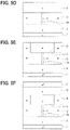
- FIG. 5A is a cross-sectional view showing a manufacturing process of the SiC semiconductor device shown in FIG. 1 .
- FIG. 5B is a cross-sectional view showing a manufacturing process of the SiC semiconductor device continued from FIG. 5A .
- FIG. 5C is a cross-sectional view showing a manufacturing process of the SiC semiconductor device continued from FIG. 5B .
- FIG. 5D is a cross-sectional view showing a manufacturing process of the SiC semiconductor device continued from FIG. 5C .
- FIG. 5E is a cross-sectional view showing a manufacturing process of the SiC semiconductor device continued from FIG. 5D .
- FIG. 5F is a cross-sectional view showing a manufacturing process of the SiC semiconductor device continued from FIG. 5E .
- FIG. 5G is a cross-sectional view showing a manufacturing process of the SiC semiconductor device continued from FIG. 5F .
- FIG. 5H is a cross-sectional view showing a manufacturing process of the SiC semiconductor device continued from FIG. 5G .
- FIG. 5I is a cross-sectional view showing a manufacturing process of the SiC semiconductor device continued from FIG. 5H .
- FIG. 5J is a cross-sectional view showing a manufacturing process of the SiC semiconductor device continued from FIG. 5I .
- FIG. 6 is a cross-sectional view of a SiC semiconductor device according to a second embodiment.
- FIG. 7A is a cross-sectional view of a SiC semiconductor device described according to a modification of the first embodiment and the second embodiment.
- FIG. 7B is a cross-sectional view of a SiC semiconductor device described according to a modification of the first embodiment and the second embodiment.
- FIG. 8 is a cross-sectional view of a SiC semiconductor device according to a third embodiment.
- FIG. 9 is a cross-sectional view of a SiC semiconductor device according to a fourth embodiment.
- FIG. 10 is an upper surface layout view showing a SiC semiconductor device according to a fifth embodiment.
- FIG. 11 is an upper surface layout view showing a SiC semiconductor device described according to a modification of the fifth embodiment.
- FIG. 12 is a cross-sectional view of a SiC semiconductor device according to a sixth embodiment.
- FIG. 13A is a cross-sectional view showing a method for manufacturing a SiC semiconductor device according to a seventh embodiment.
- FIG. 13B is a cross-sectional view showing a method for manufacturing the SiC semiconductor device continued from FIG. 13A .
- FIG. 13C is a cross-sectional view showing a method for manufacturing the SiC semiconductor device continued from FIG. 13B .
- FIG. 14A is a cross-sectional view showing a method for manufacturing a SiC semiconductor device according to an eighth embodiment.
- FIG. 14B is a cross-sectional view showing a method for manufacturing the SiC semiconductor device continued from FIG. 14A .
- FIG. 14C is a cross-sectional view showing a method for manufacturing the SiC semiconductor device continued from FIG. 14B .
- FIG. 15 is a time chart showing a growth profile of an n type impurity layer that forms a JFET portion described as an example in a ninth embodiment.
- FIG. 16 is a diagram showing a relation between a depth of the JFET portion and the n type impurity concentration.
- FIG. 17 is a time chart showing a growth profile of an n type impurity layer that forms a JFET portion described as a preferable example in the ninth embodiment.
- FIG. 18A is a cross-sectional view showing a manufacturing process of a SiC semiconductor device described in a tenth embodiment when a trench having a narrow width is formed.
- FIG. 18B is a cross-sectional view showing a manufacturing process of the SiC semiconductor device continued from FIG. 18A .
- FIG. 18C is a cross-sectional view showing a manufacturing process of the SiC semiconductor device continued from FIG. 18B .
- FIG. 18D is a cross-sectional view showing a manufacturing process of the SiC semiconductor device continued from FIG. 18C .
- FIG. 18E is a cross-sectional view showing a manufacturing process of the SiC semiconductor device continued from FIG. 18D .
- FIG. 18F is a cross-sectional view showing a manufacturing process of the SiC semiconductor device continued from FIG. 18E .
- FIG. 18G is a cross-sectional view showing a manufacturing process of the SiC semiconductor device continued from FIG. 18F .
- FIG. 19A is a cross-sectional view showing a manufacturing process of a SiC semiconductor device according to an eleventh embodiment.
- FIG. 19B is a cross-sectional view showing a manufacturing process of the SiC semiconductor device continued from FIG. 19A .
- FIG. 19C is a cross-sectional view showing a manufacturing process of the SiC semiconductor device continued from FIG. 19B .
- FIG. 19D is a cross-sectional view showing a manufacturing process of the SiC semiconductor device continued from FIG. 19C .
- FIG. 19E is a cross-sectional view showing a manufacturing process of the SiC semiconductor device continued from FIG. 19D .
- FIG. 19F is a cross-sectional view showing a manufacturing process of the SiC semiconductor device continued from FIG. 19E .
- FIG. 19G is a cross-sectional view showing a manufacturing process of the SiC semiconductor device continued from FIG. 19F .
- FIG. 19H is a cross-sectional view showing a manufacturing process of the SiC semiconductor device continued from FIG. 19G .
- FIG. 19I is a cross-sectional view showing a manufacturing process of the SiC semiconductor device continued from FIG. 19H .
- an impurity concentration of a portion of a p type base region in vicinity of a channel is different from that of a JFET portion.
- the impurity concentration of the p type base region is made to have a gradient in the depth direction so that the impurity concentration is low near the channel and becomes higher in a direction toward the bottom.
- the impurity concentration of the p type base region is low near the channel, it is possible to implement the low on-resistance.
- the JFET portion of the p type base region is provided with a desired impurity concentration so as to pinch off the n type drift layer between the adjacent p type base regions, so that a low saturation current can be implemented. Accordingly, it may be possible to achieve both low on-resistance value and low saturation current.
- the JFET resistance increases when the impurity concentration of the JFET portion of the p type base region is increased or an interval of adjacent p type base regions at the JFET portion is decreased so that a higher withstand current is obtained as a lower saturation current. Therefore, it is impossible to achieve both low on-resistance value and low saturation current.
- One example of the present disclosure provides a semiconductor device capable of achieving both low on-resistance value and low saturation current, and a method for manufacturing the same.
- a semiconductor device includes: an inversion type semiconductor element that includes: a substrate having a first conductivity type or a second conductivity type and made of semiconductor; a first conductivity type layer formed on the substrate and made of a semiconductor having the first conductivity type with an impurity concentration lower than an impurity concentration of the substrate; a second conductivity type region that is formed on the first conductivity type layer, and is made of a semiconductor having the second conductivity type; a JFET portion that is formed on the first conductivity type layer, is sandwiched by the second conductivity type region to be placed, and has, at least, a striped shape when the JFET portion is viewed from a normal direction of the substrate; a source region that is formed on the second conductivity region, and is made of a semiconductor having the first conductivity type and a concentration higher than a concentration of the first conductivity type layer; a gate insulation film formed on a channel region that is a part of the second conductivity type region; a gate electrode formed on the gate insulation film;
- the JFET portion when the voltage at the normal operation is applied as the drain voltage, the JFET portion causes the current to flow while suppressing an extension amount of a depletion layer extending from the second conductivity type region.
- the JFET portion is pinched off by the depletion layer.
- a width at the linear portion in the JFET portion is defined as W
- a first conductivity type impurity concentration is defined as Nd
- a second type impurity concentration of a portion sandwiching the JFET portion in the second conductivity type region is defined as Na
- an elementary charge is defined as q
- a dielectric constant of the semiconductor is defined as ⁇
- a vertical MOSFET is formed as a semiconductor element.
- the vertical MOSFET is formed in a cell region of the SiC semiconductor device, and the SiC semiconductor device is configured by forming an outer peripheral withstand voltage structure so as to surround the cell region.
- the vertical MOSFET is illustrated here.
- a horizontal direction in FIG. 1 is taken as a width direction
- a vertical direction is taken as a thickness direction or a depth direction.
- an n + type substrate 1 made of SiC is used as a semiconductor substrate.
- An n ⁇ type low concentration layer 2 made of SiC is formed on a main surface of the n + type substrate 1 .
- a JFET portion 2 a made of n type SiC and a p type deep layer 3 made of p type SiC are formed on the n ⁇ type low concentration layer 2 .
- the n ⁇ type low concentration layer 2 corresponds to a first conductivity type layer, and is connected to the JFET portion 2 a at a position apart from the n + type substrate 1 , that is, on the opposite side to the n + type substrate 1 .
- the p type deep layer 3 made of SiC is formed on both sides of this JFET portion 2 a .
- the JFET portion 2 a has a strip shape extending along the longitudinal direction of a trench gate structure described later, that is, a linear shape.
- the p type deep layer 3 is formed around the JFET portion 2 a , and thereby the p type deep layer 3 also has the strip shape.
- the n + type substrate 1 has the (0001) Si plane at its surface and has, for example, an n type impurity concentration of 5.9 ⁇ 10 18 /cm 3, and a thickness of 100 ⁇ m.
- the n ⁇ type low concentration layer 2 has an n type impurity concentration of 6.0 ⁇ 10 15 to 2.0 ⁇ 10 16 /cm 3 , here, has the n type impurity concentration of 1.0 ⁇ 10 16 /cm 3 .
- the n ⁇ type low concentration layer 2 has a thickness of 6 to 13 ⁇ m, for example, 8.0 ⁇ m here.
- the JFET portion 2 a has an n type impurity concentration of 3.0 ⁇ 10 17 to 3.0 ⁇ 10 18 /cm 3 , and, here, has the n type impurity concentration of 1.3 ⁇ 10 18 to 1.4 ⁇ 10 18 /cm 3 .
- the JFET portion 2 a has a width of 0.3 ⁇ m or less, and, here, has the width of 0.1 ⁇ m.
- the p type deep layer 3 has a p type impurity concentration of 5.0 ⁇ 10 17 to 2.0 ⁇ 10 18 /cm 3 , and, here, has the p type impurity concentration of 1.1 ⁇ 10 18 to 1.2 ⁇ 10 18 /cm 3 .
- the p type deep layer 3 has a thickness of 1.0 ⁇ m, for example.
- An n type current dispersion layer 4 made of SiC is formed on the JFET portion 2 a and the p type deep layer 3 , is connected to the JFET portion 2 a , and has a width wider than that of the JFET portion 2 a .
- a p type connection layer 5 made of SiC is formed on the p type deep layer 3 , and has a width narrower than that of the p type deep layer 3 .
- the n type current dispersion layer 4 is a layer that causes the current flowing through the channel region as described layer to be distributed in a width direction.
- the n type current dispersion layer 4 has a concentration higher than that of the JFET portion 2 a , and has, for example, an n type impurity concentration of 3 ⁇ 10 17 /cm 3 and a width of 0.6 ⁇ m.
- the concentration of the p type connection layer 5 may be same as the concentration of the p type deep layer 3 . However, in the present embodiment, the concentration of the p type deep layer 3 is higher than the concentration of the p type connection layer 5 .
- the p type connection layer 5 has a p type impurity concentration of 3 ⁇ 10 17 /cm 3 , and a width of 0.6 ⁇ m.
- n ⁇ type low concentration layer 2 the JFET portion 2 a , and the n type current dispersion layer 4 are described as different configurations. However, each of these n type layer functions as a drift layer.
- the p type base region 6 made of SiC is formed on the n type current dispersion layer 4 and the p type connection layer 5 , and is connected to the p type deep layer 3 via the p type connection layer 5 .
- An n + type source region 7 made of SiC and an p + type contact region 8 made of SiC are formed on the p type base region 6 .
- the n + type source region 7 is formed on a portion corresponding to the n type current dispersion layer 4 in the p type base region 6 .
- the p + type contact region 8 is formed on a portion corresponding to the p type connection layer 5 in the p type base region 6 .
- the p type base region 6 is electrically connected a source electrode 13 described later through the p + type contact region 8 .
- the p type base region 6 has a thickness thinner than that of the p type deep layer 3 , and has a p type impurity concentration lower than that of the p type deep layer 3 , and has, for example, the p type impurity concentration of 3 ⁇ 10 17 /cm 3 and the thickness of 0.3 ⁇ m.
- the n type impurity concentration of the n + type source region 7 is higher than the concentration of the n type current dispersion layer 4 .
- the p type impurity concentration of the p + type contact region 8 is higher than that of the p type base region 6 .
- a gate trench 9 has, for example, a width of 0.8 ⁇ m and a depth that is deeper than a depth obtained by adding a total film thickness of the p type base region 6 and the n + type source region 7 to a depth of 0.2 to 0.4 ⁇ m so as to penetrate the p type base region 6 and the n + type source region 7 and reach the n type current dispersion layer 4 .
- the p type base region 6 and the n + type source region 7 are placed so as to be in contact with side surfaces of this gate trench 9 .
- the gate trench 9 is provided in a linear layout with a right and left direction of the paper of FIG. 1 as the width direction, a normal direction of the paper as the longitudinal direction, and an upper and lower direction of the paper as the depth direction.
- the gate trench 9 has an arbitrary width, it is preferable that the width of the JFET portion 2 a is smaller than the width of the gate trench 9 .
- multiple gate trenches 9 are disposed at regular intervals in the left and right direction of the paper so as to be sandwiched between the p type deep layers 3 , and formed in a stripe shape.
- a pitch of the gate trench 9 that is, an arrangement interval between the adjacent gate trenches 9 is set to a cell pitch that is a pitch of one cell of the vertical MOSFET.
- a half cell pitch is half the cell pitch and is set to 1.55 ⁇ m.
- the gate trench 9 has the arbitrary width, here, the width of the gate trench 9 is smaller than the half cell pitch.
- a gate insulation film 10 is formed on an inner wall surface of the gate trench 9 including a channel region.
- the channel region is a portion of the p type base region 6 located on a side surface of the gate trench 9 and, is a channel region connecting the n + type source region 7 and the n type current dispersion layer 4 when the vertical MOSFET is operated.
- a gate electrode 11 made of doped Poly-Si is formed on the surface of the gate insulation film 10 , and the inside of the gate trench 9 is filled with the gate insulation film 10 and the gate electrode 11 .
- a source electrode 13 or the like is formed via an interlayer insulation film 12 .
- the source electrode 13 is made of multiple metals, for example, Ni/Al or the like.
- a portion contacting to the gate electrode 11 is made of a metal capable of ohmic contact with the n type SiC.
- At least a portion contacting with, among the multiple metals, at least the p type SiC, specifically, a portion contacting with the p + type contact region 8 is made of a metal capable of ohmic contact with the p type SiC.
- the source electrode 13 is electrically insulated by being formed on the interlayer insulation film 12 .
- the source electrode 13 is electrically connected to the n + type source region 7 and the p + type contact region 8 through contact holes formed in the interlayer insulation film 12 .
- a drain electrode 14 electrically connected to the n + type substrate 1 is formed on the back side of the n + type substrate 1 .
- the n channel type vertical MOSFET having an inversion type trench gate structure is formed.
- the cell region is provided by arranging such vertical MOSFETs for multiple cells.
- the SiC semiconductor device is provided by forming the outer peripheral voltage withstand structure such as a guard ring (not shown) or the like so as to surround the cell region in which such vertical MOSFETs are formed.
- the SiC semiconductor device including the vertical MOSFET configured as described above is operated by, for example, applying a gate voltage Vg of 20 V to the gate electrode 11 in a state where the source voltage Vs is 0 V and the drain voltage Vd is, for example, 1 to 1.5 V. That is, when the gate voltage is applied, the vertical MOSFET performs an operation in which a channel region is formed in a portion of the p type base region 6 that contacts with the gate trench 9 and a current flows between the drain and the source.
- the concentration of the JFET portion 2 a is high and the JFET portion 2 a is sandwiched by the p type deep layers 3 , that is, a configuration having a narrow width is formed. Therefore, this JFET portion 2 a functions as a depletion layer adjustment layer, and thereby the following operation is performed.
- a depletion layer extends from a side of the p type deep layer 3 to the JFET portion 2 and an extending width of the depletion layer is smaller than the width of the JFET portion 2 a . That is, the JFET portion 2 a functions as a layer that stops the extension of the depletion layer. Therefore, it is possible to suppress the extension of the depletion layer into the JFET portion 2 a and to suppress the current path from becoming narrow, and therefore, it becomes possible to achieve the low on-resistance.
- the JFET portion 2 a Since the JFET portion 2 a has a high n type impurity concentration and a low resistance, the JFET portion 2 a functions as a current path, and therefore, it is possible to further reduce the on-resistance.
- the width of the JFET portion 2 a and the impurity concentrations of the JFET portion 2 a and the p type deep layer 3 are set so that the JFET portion 2 a is pinched off when the drain voltage Vd is slightly higher than the drain voltage Vd at the normal operation. Thereby, the JFET portion 2 a can be pinched off even at the low drain voltage Vd. In this way, when the drain voltage Vd becomes higher than the voltage at the normal operation, the JFET portion 2 a is immediately pinched off, so that a low saturation current can be maintained. It becomes possible to improve the tolerance of the SiC semiconductor device due to the load short circuit or the like.
- the SiC semiconductor device capable of achieving both low on-resistance value and low saturation current.
- the p type deep layer 3 is projected toward a center line of the gate electrode 11 as compared with the p type base region 6 , and thereby the width of the JFET portion 2 a is narrowed Therefore, even when the drain voltage Vd becomes a high voltage, the extension of the depletion layer extending from the bottom to the n ⁇ type low concentration layer 2 is suppressed by the p type deep layer 3 . Thereby, it may be possible to prevent the depletion layer from extending into the trench gate structure. Accordingly, it may be possible to reduce the electric field to the gate insulation film 10 , and provide a highly reliable element.
- the SiC semiconductor device in the present embodiment includes the semiconductor element of a normally-off type in which no current flows between the drain and the source when the gate voltage Vg is not applied, since the channel region is not formed.
- the JFET portion 2 a is a normally-on type since it pinches off only when the drain voltage Vd is higher than the voltage at the normal operation, even in the case where the gate voltage Vg is not applied.
- Vd-Id characteristics of a present embodiment structure having the narrowed width of the JFET portion 2 a and the high n type impurity concentration and a comparative example structure are compared.
- the Vd-Id characteristics are characteristics of a drain current Id with respect to the drain voltage Vd.
- the comparative example structure is a structure that does not include the p type deep layer 3 .
- the p type connection layer 5 is formed so as to reach a depth same as that of the p type deep layer 3 , and the n type impurity concentration of the JFET portion 2 a is lower than that of the present embodiment.
- FIG. 3 shows a comparison result obtained by the simulation, and shows characteristics when the gate voltage is 20 [V], the source voltage Vs is 0 [V], and the drain voltage Vd is changed.
- the on-resistance could be a low value of 3.3 [m ⁇ cm 2 ].
- the SiC semiconductor device of the present embodiment even when the drain voltage Vd becomes the high voltage, the drain current Id can be reduced. Therefore, it may be possible to achieve the low saturation current.
- FIG. 4 shows a comparison result of Vd-Cgd characteristics of the present embodiment structure and the comparative example structure.
- the Vd-Cgd characteristics are characteristics of the gate-drain capacitance Cgd with respect to the drain voltage Vd.
- the gate-drain capacitance Cgd was about 30 [pF].
- the gate-drain capacitance Cgd is 30 [fF], that is, reduced by four digits. Thereby, in the present embodiment structure, it may be possible to reduce the gate-drain capacitance Cgd, and improve the switching speed.
- the SiC semiconductor device capable of achieving both low on-resistance value and low saturation current. Further, it may be possible to provide the SiC semiconductor device capable of improving the switching speed.
- the impurity concentrations and the dimensions of the JFET portion 2 a and the p type deep layer 3 or the like are shown, these are merely examples.
- the impurity concentrations and the dimensions of the JFET portion 2 a and the P type deep layer 3 are set so as to satisfy desired pinch-off conditions.
- the impurity concentrations and the dimensions of the JFET portion 2 a and the p type deep layer 3 are set so that the JFET portion 2 a is pinched off earlier than the vertical MOSFET. That is, when the width of the JFET portion 2 a is defined as W, the n type impurity concentration is defined as Nd, the p type impurity concentration of the p type deep layer 3 is defined as Na, an elementary charge is defined as q, a dielectric of SiC is defined as ⁇ , the following expression is established. 90[V]>( q ⁇ Nd ⁇ ( Na+Nd ) ⁇ W 2 )/2 ⁇ Na (Mathematical expression)
- This mathematical expression is set as a condition capable of achieving both low on-resistance and low saturation current.
- the maximum value indicates the voltage value set as the pinch-off condition, and defines the drain voltage at which the JFET portion 2 a surly pinches off even when an activation rate of a process or an ionization rate is taken into consideration.
- the n + type substrate 1 is prepared as the semiconductor substrate.
- the n ⁇ type low concentration layer 2 made of SiC is formed on the main surface of the n + type substrate 1 .
- the p type deep layer 3 made of SiC is formed.
- the p type deep layer 3 is formed by ion implantation of the p type impurities into a surface layer of the n ⁇ type low concentration layer 2 or the epitaxial growth on the n ⁇ type low concentration layer 2 .
- a mask (not shown) that opens a position corresponding to JFET portion 2 a is formed on the p type deep layer 3 .
- the p type deep layer 3 is removed, and a trench 3 a is formed.
- the n ⁇ type low concentration layer 2 is exposed at the bottom of the trench 3 a.
- the JFET portion 2 a is formed by selectively performing embedded epitaxial growth in a state where a surface of the p type deep layer 3 other than the trench 3 a is covered by the mask. Thereby, the JFET portion 2 a is formed so as to fill the trench 3 a . Thereafter, the mask (not shown) is removed. The surface of the p type deep layer 3 , a high concentration n type layer 20 , or the JFET portion 2 a are flattened as needed.
- the n type current dispersion layer 4 is epitaxially grown on the surface of the p type deep layer 3 or the JFET portion 2 a.
- the p type connection layer 5 is formed by ion-implanting the p type impurity at a position apart from the JFET portion 2 a in the n type current dispersion layer 4 .
- the p type base region 6 and the n + type source region 7 are epitaxially grown on the n type current dispersion layer 4 and the p type connection layer 5 .
- the p + type contact region 8 is formed by ion-implanting the p type impurity into a part of the n + type source region 7 .
- the gate trench 9 is formed by performing anisotropic etching such as RIE (Reactive Ion Etching) or the like.
- the gate insulation film 10 covers an inner wall surface of the gate trench 9 and the surface of the n + type source region 7 .
- a Poly-Si doped with the p type impurity or the n type impurity is deposited, and then etched back to leave at least the Poly-Si in the gate trenches 9 , thereby the gate electrode 11 is formed.
- the interlayer insulation film 12 made of, for example, an oxide film is formed so as to cover the surfaces of the gate electrode 11 and the gate insulation film 10 .
- the mask (not shown) has been formed on a surface of the interlayer insulation film 12 , the mask is opened at portions located between the gate electrodes 11 , that is, the portions corresponding to the p + type contact region 8 and the vicinity of the p type contact region 8 .
- the interlayer insulation film 12 is patterned by using the mask to form contact holes exposing the p + type contact region 8 and the n + type source region 7 .
- the electrode material provided by, for example, a laminated structure of multiple metals is formed on the surface of the interlayer insulation film 12
- the source electrode 13 is formed by patterning the electrode material.
- the drain electrode 14 is formed on the back side of the n + type substrate 1 . Thereby, the SiC semiconductor device according to the present embodiment is completed.
- the SiC semiconductor device of the present embodiment has a narrow structure in which the JFET portion 2 a has the high concentration and the JFET portion 2 a is sandwiched by the p type deep layers 3 protruding from both sides. Therefore, at the normal operation, it may be possible to suppress the extension of the depletion layer into the JFET portion 2 a and suppress the current path from becoming narrow, and therefore, it becomes possible to achieve the low on-resistance.
- the JFET portion 2 a Since the JFET portion 2 a has the high n type impurity concentration and the low resistance, the JFET portion 2 a functions as the current path, and therefore, it is possible to further reduce the on-resistance.
- the width of the JFET portion 2 a and the impurity concentrations of the JFET portion 2 a and the p type deep layer 3 are set so that the JFET portion 2 a is pinched off when the voltage is slightly higher than the drain voltage Vd at the normal operation. Thereby, the JFET portion 2 a can be pinched off even at the low drain voltage Vd. In such a manner, when the drain voltage Vd becomes higher than the voltage at the normal operation, the JFET portion 2 a is immediately pinched off, so that a low saturation current can be maintained. It becomes possible to improve the tolerance of the SiC semiconductor device due to the load short circuit or the like.
- the SiC semiconductor device capable of achieving both low on-resistance value and low saturation current.
- a second embodiment will be described.
- the configuration between the JFET portion 2 a and the n ⁇ type low concentration layer 2 and the configuration between the p type deep layer 3 and the n ⁇ type low concentration layer 2 are modified with respect to the first embodiment, and the other configurations are similar to the first embodiment. Only features different from the first embodiment will be described.
- the SiC semiconductor device of the first embodiment has a structure that additionally includes a high concentration n type layer 20 at a boundary position between the JFET portion 2 a and the n ⁇ type low concentration layer 2 and between the p type deep layer 3 and the n ⁇ type low concentration layer 2 .
- the concentration of the high concentration n type layer 20 is higher than the concentration of the n ⁇ type low concentration layer 2 .
- the impurity concentration of the high concentration n type layer 20 is same as the impurity concentration of the JFET portion 2 a .
- the impurity concentration of the high concentration n type layer 20 may be different from the impurity concentration of the JFET portion 2 a .
- a thickness of the high concentration n type layer 20 is, for example, 0.07 ⁇ m.
- the high concentration n type layer 20 when the high concentration n type layer 20 is arranged be the JFET portion 2 a and the p type deep layer 3 , it is possible to further reduce the on-resistance in accordance with the high concentration n type layer 20 .
- the extension of the depletion layer extending from the p type deep layer 3 towards the n ⁇ type low concentration layer 2 may become larger as compared with the case where the high concentration n type layer 20 is included.
- the current path of the n ⁇ type low concentration layer 2 in vicinity of the JFET portion 2 a may be narrowed.
- the high concentration n type layer 20 is included as shown in the present embodiment, and thereby it may be possible to suppress the current path of the n ⁇ type low concentration layer 2 in the vicinity of the JFET portion 2 a , and may be possible to more achieve the low on-resistance.
- the method for manufacturing the SiC semiconductor device of the present embodiment is almost the same as the first embodiment. That is, after the n ⁇ type low concentration layer 2 is formed as described in the first embodiment, next, the high concentration n type layer 20 is forming by increasing the introduction amount of gas that becomes the n type impurity or the like. Thereafter, by performing each of the process of FIG. 5B and subsequent processes, the SiC semiconductor device of the present embodiment can be manufactured.
- the structures described in the first embodiment and the second embodiment described above may be structures, as shown in FIG. 7A and FIG. 7B , in which the JFET portion 2 a protrudes to a position lower than the p type deep layer 3 , more specifically, the n ⁇ type low concentration layer 2 .
- a third embodiment will be described.
- the present embodiment is the similar to the first and second embodiments except that a super junction structure is applied to the first and second embodiments. Only the differences from the first and second embodiments will be described.
- the super junction structure is applied to the vertical MOSFET of the structure of the first embodiment.
- the super junction structure can be applied to the vertical MOSFET having the high concentration n type layer 20 as shown in the second embodiment.
- a p type column layer 40 extending toward the n type low concentration layer 2 at a position lower than the p type deep layer 3 is included.
- the p type column layer 40 is in contact with the n + type substrate 1 .
- the p type column layer 40 may be separated from the n + type substrate 1 .
- the PN junction super junction structure in which the n ⁇ type low concentration layer 2 is the n type column layer is formed.
- the JFET portion 2 a and the P type deep layer 3 are formed as in the first embodiment, so that it may be possible to obtain the similar effects to the first embodiment.
- the SiC semiconductor device of the present embodiment structure can be basically manufactured by the similar manufacturing method to that of the first embodiment.
- the p type column layer 40 can be formed by forming the trench in the n ⁇ type low concentration layer 2 , performing the embedded epitaxial growth, and further etching back to flatten the surface of the p type column layer 40 . Except for this, the SiC semiconductor device can be manufactured by the similar method to that of the first embodiment.
- a fourth embodiment will be described.
- the present embodiment is obtained by changing the contact structure of the source electrode 13 in the first to third embodiments, and the other configuration is the similar to the first to third embodiments, and therefore only the portions different from the first to third embodiments will be described.
- the change of the contact structure of the source electrode 13 is applied to the vertical MOSFET in the first embodiment.
- the change may be applied to the vertical MOSFETs in the second and third embodiments.
- contact trench 50 is formed on the opposite side of the trench gate structure and sandwiches the n + type source region 7 .
- the p + type contact region 8 is formed at the surface layer portion of the p type base region 6 .
- Such a structure can be implemented by forming the n + type source region 7 , then forming the contact trench 50 by the etching, and thereafter per the ion-implantation for forming the p + type contact region 8 .
- the contact between the source electrode 13 and the p type base region 6 may be achieved by the contact trench 50 formed by removing a part of the n + type source region 7 .
- a fifth embodiment will be described.
- the present embodiment is obtained by changing an upper surface layout of the JFET portion 2 a in the first to fourth embodiments, and the other configuration is the similar to the first to fourth embodiments, and therefore only the portions different from the first to fourth embodiments will be described.
- the change of the layout configuration is applied to the vertical MOSFET having the structure in the first embodiment.
- the change may be applied to the vertical MOSFETs in the second to fourth embodiments.
- the JFET portion 2 a is formed in the strip shape along a longitudinal direction of the trench gate structure.
- the JFET portion 2 a is laid out so as to intersect with the longitudinal direction of the trench gate structure, here, at the right angle. Thereby, the trench gate structure and the JFET portion 2 a are laid out in a lattice shape.
- the width of the JFET portion 2 a indicates a width of each linear shaped portion forming the lattice shape.
- the layout is not limited to the layout in which the trench gate structure and the JFET portion 2 a are formed in the lattice shape, and may be a different layout.
- the JFET portion 2 a may be formed in a frame shape such as a quadrangle, and each JFET portion 2 a may be arranged in the lattice shape.
- the width of the JFET portion 2 a indicates a width of a linear shaped portion of the frame shape.
- a sixth embodiment will be described.
- a vertical MOSFET having a planar structure is employed and the other features are similar to the first to fifth embodiments. Only differences from the first to fifth embodiments will be described.
- the planar structure is applied to the vertical MOSFET having the structure in the second embodiment.
- the planar structure can be applied to the vertical MOSFETs having the structure in the first embodiment and the third to fifth embodiments.
- the structure having the JFET portion 2 a with the high concentration can be applied to the SiC semiconductor device having the vertical MOSFET of the planar structure as shown in FIG. 12 .
- the high concentration n type layer 20 or the p type base region 6 is formed on the n ⁇ type low concentration layer 2
- the n + type source region 7 is formed on a surface portion of the p type base region 6 .
- the JFET portion 2 a is formed so as to be sandwiched by the P type base regions 6 .
- a surface side of a portion between the n + type source region 7 and the JFET portion 2 a in the p type base region 6 is formed as the channel region.
- the gate electrode 11 is formed on the channel region through the gate insulation film 10 .
- the high concentration n type layer 20 is formed on the upper surface of the n ⁇ type low concentration layer 2 . Therefore, the amount of the extension of the depletion layer extending from the p type base region 6 to the side of the n ⁇ type low concentration layer 2 is also suppressed. It may be possible to more reduce the on-resistance.
- a seventh embodiment will be described.
- the present embodiment is obtained by changing a formation method of the JFET portion 2 a in the first to sixth embodiments, and the other configuration is the similar to the first to sixth embodiments, and therefore only the portions different from the first to sixth embodiments will be described.
- the manufacturing method in the present embodiment is applied to the vertical MOSFET having the structure in the first embodiment.
- the planar structure can be applied to the vertical MOSFETs having the structure in each of the second to sixth embodiments.
- the JFET portion 2 a is formed by a different way.
- the n ⁇ type low concentration layer 2 and the p type deep layer 3 are epitaxially grown on the n + type substrate 1 .
- a mask 30 having an opening at a predetermined region, that is, a region where the JFET portion 2 a is to be formed is formed on the p type deep layer 3 .
- the JFET portion 2 a is formed by ion-implanting the n type impurities from the above of the mask 30 and performing activation annealing. Thereafter, after the mask 30 is removed, the similar processes to FIGS. 5D to 5J are performed. Thereby, the SiC semiconductor device having the vertical MOSFET similar to that of FIG. 1 can be manufactured.
- the JFET portion 2 a can be also formed by the ion-implantation. Even when the SiC semiconductor device is manufactured by such a manufacturing method, it may be possible to provide the similar effect to the first embodiment.
- the present embodiment is obtained by changing a formation method of the p type connection layer 5 and the p + type contact region 8 in the first to seventh embodiments, and the other configuration is the similar to the first to seventh embodiments, and therefore only the portions different from the first to seventh embodiments will be described.
- the manufacturing method in the present embodiment is applied to the vertical MOSFET having the structure in the first embodiment.
- the planar structure can be applied to the vertical MOSFETs having the structure in the second to seventh embodiments.
- FIGS. 5A to 5D described in the first embodiment are performed.
- the p type connection layer 5 is not formed at the n type current dispersion layer 4 , and the p type base region 6 and the n + type source region 7 are formed.
- the trench gate structure is formed.
- a trench 60 is formed at a position apart from the trench gate structure, penetrates the n + type source region 7 or the p type base region 6 and the n type current dispersion layer 4 , and reaches the p type deep layer 3 .
- a p type layer 61 is formed by the embedded epitaxial growth, and functions as the p type connection layer 5 and the p + type contact region 8 .
- the p type layer 61 functioning as the p type connection layer 5 and the p + type contact region 8 may be formed by the epitaxial growth.
- a ninth embodiment will be described.
- the present embodiment provides a more preferable manufacturing process of the JFET portion 2 a in the first to sixth embodiments and the eighth embodiment, and the other is the similar to the first embodiment, and therefore only the portions different from the method will be described.
- the p type deep layer 3 is removed, the trench 3 a is formed, the epitaxial growth filling this trench 3 a is performed, and thereby the JFET portion 2 a is formed.
- the trench 3 a having a narrow width of 0.1 ⁇ m or less is filled by the epitaxial growth, it was confirmed that the n type impurity concentration of the JFET portion 2 a at the bottom of the trench 3 a is higher than that at the shallower position.
- a growth profile shown in FIG. 15 can be applied.
- a sample is placed in an epitaxial growth device. After a temperature rising period, the sample is heated at a predetermined temperature. For example, in the temperature rising period, while H 2 (hydrogen) that becomes carrier gas is introduced in the epitaxial growth device, heating is performed for about 40 minutes, and the temperature of the sample is raised up to 1650° C. While the constant temperature is kept, N 2 (nitrogen) that becomes the n type dopant, SiH 4 (silane) that becomes SiC source gas, and C 3 H 3 (propane) are simultaneously supplied.
- H 2 hydrogen
- SiH 4 silane
- C 3 H 3 propane
- the JFET portion 2 a can be formed.
- the n type impurity concentration at the bottom of the trench 3 a shown in FIG. 16 is higher than that at the shallower portion. Therefore, for example, the n type impurity concentration of the JFET portion 2 a at the bottom of the trench 3 a is higher than the target value, and the n type impurity concentration at the shallower portion is lower than the target value.
- the n type impurity concentration at the higher portion is about 4 ⁇ 10 18 cm ⁇ 3
- the n type impurity concentration at the lower portion is about 1.0 ⁇ 10 17 cm ⁇ 3 . There is a difference of one digit or more.
- the JFET portion 2 a is formed according to the growth profile shown in FIG. 17 so that the n type impurity concentration of the JFET portion 2 a more approaches the target value.
- the JFET portion 2 a is formed according to the similar profile to the above described profile of FIG. 15 , the N 2 that becomes the n type dopant is not supplied at an initial stage of the growth when the JFET portion 2 a is epitaxially grown after the temperature rising period. That is, at the initial stage of the growth, a undoped period in which only SiH 4 and C 3 H 8 that become the SiC source gases are introduced, and the N2 that becomes the n type dopant is not introduced is provided.
- the JFET portion 2 a is embedded in the trench 3 a having the width of 0.1 ⁇ m, the JFET portion 2 a can be embedded by performing the epitaxial growth for about two minutes.
- the undoped period is set to 5 to 60 seconds, for example, 10 seconds. After the initial stage of the growth, the undoped period elapses. Thereafter, the supply of N 2 that becomes n type dopant as a delay dope starts.
- the n type impurity concentration at the bottom of the trench 3 a is prevented from becoming high, and the n type impurity concentration in the entire of the JFET portion 2 a can be mostly uniformized at the target value.
- the n type impurity concentration of the JFET portion 2 a may be suppressed from becoming uneven by providing the undoped period when the JFET portion 2 a is epitaxially grown. Therefore, the n type impurity concentration of the JFET portion 2 a can be brought closer to the target value, and the SiC semiconductor device can have better characteristics.
- the JFET portion 2 a is formed by selectively performing the embedded epitaxial growth in a state where the surface of the p type deep layer 3 other than the trench 3 a is covered by the mask.
- the mask may be omitted, and the JFET portion 2 a may be formed.
- the n type SiC for forming the JFET portion 2 a is formed outside the trench 3 a .
- it may be sufficient to etch back the portion formed outside the trench 3 a in the n type SiC to remove the formed portion.
- the H 2 when the H 2 is used as the carrier gas, the H 2 can be used as the etching gas.
- the formation of the JFET portion 2 a is completed and the supply of the N 2 that becomes the n type dopant or the SiH 4 and C 3 H 8 that become the SiC source gas is stopped, it may be possible to etch back the unnecessary portion of the n type SiC formed at the time of forming the JFET portion 2 a by continuing the supply of the H 2 . Further, since the unnecessary portion of the n type SiC can be etched back in such a manner, the epitaxial growth of the n type current dispersion layer 4 can be continuously performed by keeping the use of the same epitaxial growth device without lowering the temperature while maintaining the temperature.
- the p type base region 6 and the n + type source region 7 can be epitaxially grown without lowering the temperature, and the trench 60 shown in FIG. 14B can be formed. In such a manner, it may be possible to simplify the manufacturing process, and reduce the manufacturing cost.
- a tenth embodiment will be described.
- the present embodiment provides a more preferable formation process of the trench 3 a in which the JFET portion 2 a is embedded, the formation process being described in the first embodiment.
- the other is the similar to the first embodiment, and therefore only the portions different from the first embodiment will be described.
- This method can be applied to not only the first embodiment but also the second to sixth, eighth, and ninth embodiments.
- the process shown in FIG. 5B is described above.
- the mask opening the position corresponding to the JFET portion 2 a is formed on the p type deep layer 3 and the etching using the mask is performed.
- the trench 3 a can be formed by performing the process.
- a minimum formation line width may be lower than, for example, 0.3 ⁇ m.
- the better formation of the narrow width of the trench 3 a may not be performed. Therefore, as the formation process of the trench 3 a , it is preferable to perform the processes shown in FIGS. 18A to 18G .
- the process other than the formation process of the trench 3 a is similar to that of the first embodiment. Only the formation process of the trench 3 a will be described.
- the n ⁇ type low concentration layer 2 and the p type deep layer 3 are formed on the n + type substrate 1 .
- a first mask film 70 made of, for example, a TEOS (Tetra Ethyl Ortho Silicate) film is formed on the p type deep layer 3 .
- the resist 71 is exposed by using an exposure mask (not shown) and further developed to form the resist mask. Then, an opening 71 a having a width wider than that of the trench 3 a is formed at a position corresponding to a position in which the trench 3 a is to be formed.
- the width of the opening 71 a is arbitrary. However, when the width of the trench 3 a is, for example, 0.1 ⁇ m, the width of the opening 71 a is about 0.3 ⁇ m.
- the first mask film 70 is etched by using the resist 71 as the mask. Thereby, an opening 70 a having the same width as the opening 71 a of the resist 71 is formed in the first mask film 70 .
- the resist 71 is peeled, and the first mask film 70 is exposed.
- a second mask film 72 is formed on a side surface of the first mask film 70 in the opening 71 a , a surface of the p type deep layer 3 , and a surface of the first mask film 70 . Then, a film thickness of the second mask film 72 is half the value obtained by subtracting the target width of the trench 3 a from the width of the opening 70 a . For example, when the width of the opening 70 a is 0.3 ⁇ m and the target width of the trench 3 a is 0.1 ⁇ m, the film thickness of the second mask film 72 is 0.1 ⁇ m.
- the second mask film 72 is removed by anisotropic etching. Thereby, the second mask film 72 on the surface of the first mask film 70 and the second mask film 72 on the surface of the p type deep layer 3 in the opening 70 a are removed, and the second mask film 72 only on the side surface of the first mask film 70 in the opening 70 a remains. Therefore, an opening 72 a is formed by the second mask film 72 .
- a width of the opening 72 a is equal to the target width of the trench 3 a .
- the opening 72 a having a line width narrower than that of the opening 70 a can be formed.
- the first mask film 70 and the second mask film 72 as the mask, a portion exposed from the opening 72 a in the p type deep layer 3 is etched. Thereby, it may be possible to satisfactorily form the trench 3 a having the target width of, for example, 0.1 ⁇ m.
- the second mask film 72 is placed in the opening 70 a formed in the first mask film 70 .
- the opening 72 a having the narrower line width is obtained.
- the trench 3 a having the dimension exceeding a resolution of the i-line exposure machine, that is, the width narrower than the minimum formation line width can be satisfactorily formed.
- Such a trench formation process is not limited to a case of forming the JFET portion 2 a , and may be applied to a case of forming a trench for different purposes.
- the n + type substrate 1 is prepared as the semiconductor substrate
- the n ⁇ type low concentration layer 2 is formed on the main surface of the n + type substrate 1 .
- a lower layer 81 a of a p type RESURF layer 81 and a p type guard ring layer 82 are formed.
- the trench 3 a and the JFET portion 2 a are formed in the cell region as in the processes shown in FIG. 5B and FIG. 5C .
- the n type current dispersion layer 4 is epitaxially grown also in the outer peripheral region.
- an upper layer portion 81 b of the p type RESURF layer 81 is simultaneously formed.
- the outer peripheral withstand voltage structure can be also simultaneously formed in the outer peripheral region. Therefore, it may be possible to simplify the manufacturing process of the SiC semiconductor device.
- the above embodiments are not independent of each other, and can be appropriately combined together except when the combination is obviously impossible.
- the width of the JFET portion 2 a does not need to be constant in the entire region in the depth direction, and may have, for example, a tapered cross-section such that the width gradually decreases toward the drain electrode 14 .
- the layout of the JFET portion 2 a includes, at least, the linear portion when viewed from the normal direction of the n+ type substrate 1 . It may be sufficient that the width at the linear portion satisfies the pinch-off condition.
- the impurity concentration of each portion may not be constant.
- the structure may be a structure having an impurity concentration gradient in which, the p type impurity concentration decreases as the p type deep layer 3 approaches the drain electrode 14 , and the p type impurity concentration increases as the p type deep layer 3 approaches the source electrode 13 .
- the dimension and the impurity concentration of each portion configuring the SiC semiconductor device described in each of the embodiments described above, are merely examples.
- the dimension and the impurity concentration of each portion may be appropriately set based on the pinch-off condition of the JFET portion 2 a or the like.
- the half cell pitch can be set to be wider or the like, that is, the half cell pitch can be changed.
- the half cell pitch can be set to 3 ⁇ m.
- the thickness of the n type current dispersion layer 4 or the p type connection layer 5 can be thin, and the impurity concentration can be high.
- the thickness is 0.4 ⁇ m.
- the n type impurity concentration or the p type impurity concentration of each of the n type current dispersion layer 4 or the p type connection layer 5 can be 6.0 ⁇ 10 17 /cm 3 .
- the thickness of the p type deep layer 3 can be thin, and the impurity concentration can be high.
- the thickness is 0.6 ⁇ m.
- the p type impurity concentration can be 2.0 ⁇ 10 18 /cm 3 .
- these described here are also examples, and other dimensions and impurity concentrations may be used.
- the p type layer 61 is formed by embedding the trench 60 .
- the similar structure can be formed by the ion-implantation. That is, after the epitaxial growth of the n type current dispersion layer 4 , the p type base region 6 , and the n+ type source region 7 are continuously performed, the mask opening the region in which the p type layer 61 is to be formed is placed on the n+ type source region 7 . With use of the mask, the p type impurities are ion-implanted. In such a manner, the p type layer 61 functioning as the p type connection layer 5 and the p + type contact region 8 can be simultaneously formed by using the same mask. Therefore, it may be possible to simplify the manufacturing process, and reduce the manufacturing cost.
- the n channel vertical MOSFET in which the first conductivity type is n type and the second conductivity type is p type is described as an example.
- a p channel type vertical MOSFET in which the conductivity types of respective constituent are inverted may be used.
- the vertical MOSFET has been described as an example of the semiconductor element.
- the present disclosure is applicable to an IGBT which has a similar structure. In the IGBT, only the conductivity type of the n + type substrate 1 is changed from the n type to the p type with respect to each of the above embodiments, and other structures and manufacturing methods are the same as those of the above embodiments.
- the SiC semiconductor device has been described as an example in the embodiments described above, the present disclosure can be applied to a semiconductor device using Si. Specifically, each of the above embodiments can be applied to a wide band gap semiconductor device, for example, a semiconductor device using GaN, diamond, AlN, or the like.
Landscapes
- Junction Field-Effect Transistors (AREA)
- Semiconductor Integrated Circuits (AREA)
- Metal-Oxide And Bipolar Metal-Oxide Semiconductor Integrated Circuits (AREA)
Abstract
Description
90[V]>(q×Nd×(Na+Nd)×W 2)/2εNa (Mathematical expression)
Claims (16)
Applications Claiming Priority (7)
| Application Number | Priority Date | Filing Date | Title |
|---|---|---|---|
| JP2018-053155 | 2018-03-20 | ||
| JPJP2018-053155 | 2018-03-20 | ||
| JP2018053155 | 2018-03-20 | ||
| JPJP2019-041851 | 2019-03-07 | ||
| JP2019041851A JP7099369B2 (en) | 2018-03-20 | 2019-03-07 | Semiconductor devices and their manufacturing methods |
| JP2019-041851 | 2019-03-07 | ||
| PCT/JP2019/011537 WO2019181962A1 (en) | 2018-03-20 | 2019-03-19 | Semiconductor device, and production method for same |
Related Parent Applications (1)
| Application Number | Title | Priority Date | Filing Date |
|---|---|---|---|
| PCT/JP2019/011537 Continuation WO2019181962A1 (en) | 2018-03-20 | 2019-03-19 | Semiconductor device, and production method for same |
Publications (2)
| Publication Number | Publication Date |
|---|---|
| US20210005744A1 US20210005744A1 (en) | 2021-01-07 |
| US11476360B2 true US11476360B2 (en) | 2022-10-18 |
Family
ID=68066269
Family Applications (1)
| Application Number | Title | Priority Date | Filing Date |
|---|---|---|---|
| US17/025,213 Active 2039-06-04 US11476360B2 (en) | 2018-03-20 | 2020-09-18 | Semiconductor device and method for manufacturing the same |
Country Status (3)
| Country | Link |
|---|---|
| US (1) | US11476360B2 (en) |
| JP (1) | JP7099369B2 (en) |
| CN (1) | CN112262478B (en) |
Cited By (2)
| Publication number | Priority date | Publication date | Assignee | Title |
|---|---|---|---|---|
| US20240290881A1 (en) * | 2018-01-29 | 2024-08-29 | Renesas Electronics Corporation | Semiconductor device and manufacturing method thereof |
| EP4521882A1 (en) * | 2023-09-08 | 2025-03-12 | LX Semicon Co., Ltd. | Power semiconductor device and power converter including the same |
Families Citing this family (18)
| Publication number | Priority date | Publication date | Assignee | Title |
|---|---|---|---|---|
| JP2021057552A (en) * | 2019-10-02 | 2021-04-08 | ルネサスエレクトロニクス株式会社 | Semiconductor device and manufacturing method for the same |
| JP7472477B2 (en) * | 2019-12-02 | 2024-04-23 | 富士電機株式会社 | METHOD FOR MANUFACTURING SILICON CARBIDE SEMICONDUCTOR DEVICE AND METHOD FOR MANUFACTURING SILICON CARBIDE SUBSTRATE |
| CN110957351B (en) * | 2019-12-17 | 2025-04-04 | 华羿微电子股份有限公司 | A super junction MOSFET device and preparation method thereof |
| CN111048584B (en) * | 2019-12-23 | 2021-05-11 | 复旦大学 | A kind of high linearity gallium nitride HBT radio frequency power device and preparation method thereof |
| US20210399128A1 (en) * | 2020-06-19 | 2021-12-23 | Cree, Inc. | Power devices with a hybrid gate structure |
| JP7458257B2 (en) | 2020-07-09 | 2024-03-29 | 株式会社東芝 | Semiconductor devices, inverter circuits, drive devices, vehicles, and elevators |
| JP2022021181A (en) * | 2020-07-21 | 2022-02-02 | 株式会社デンソー | Semiconductor device |
| JP7521401B2 (en) * | 2020-12-11 | 2024-07-24 | 株式会社デンソー | Silicon carbide semiconductor device and manufacturing method thereof |
| CN112928166A (en) * | 2021-03-31 | 2021-06-08 | 厦门芯一代集成电路有限公司 | Novel groove grid type MOS device and preparation method thereof |
| WO2022224883A1 (en) * | 2021-04-20 | 2022-10-27 | 富士電機株式会社 | Semiconductor device |
| CN113241381B (en) * | 2021-05-24 | 2024-05-14 | 厦门芯一代集成电路有限公司 | High-voltage trench gate MOS device and preparation method thereof |
| CN113488522A (en) * | 2021-06-07 | 2021-10-08 | 西安电子科技大学 | Semi-super-junction MOSFET device with channel buffer layer and preparation method thereof |
| JP7698787B2 (en) * | 2021-11-17 | 2025-06-25 | 湖北九峰山実験室 | SILICON CARBIDE SEMICONDUCTOR DEVICE AND MANUFACTURING METHOD THEREOFThis application claims priority to a Chinese patent application, filed on November 17, 2021 with the China Patent Office, application number 202111363503.1, and entitled "SILICON CARBIDE SEMICONDUCTOR DEVICE AND MANUFACTURING METHOD THEREOF", the entire contents of which are incorporated herein by reference.This application claims priority to a Chinese patent application, filed on November 17, 2021 with the China Patent Office, application number 202122827400.8, and entitled "SILICON CARBIDE SEMICONDUCTOR DEVICE", the entire contents of which are incorporated herein by reference. |
| US20240282810A1 (en) * | 2022-01-04 | 2024-08-22 | Hubei Jiufengshan Laboratory | Silicon carbide mosfet device and manufacturing method therefore |
| JP7765318B2 (en) | 2022-03-17 | 2025-11-06 | 株式会社東芝 | Semiconductor Devices |
| WO2025183975A1 (en) * | 2024-03-01 | 2025-09-04 | Semiconductor Components Industries, Llc | Electronic device including a power transistor including a buried shield and a gap region and a process of making the same |
| CN118156311A (en) * | 2024-03-21 | 2024-06-07 | 南京第三代半导体技术创新中心有限公司 | Multi-groove silicon carbide trench gate MOSFET power device and manufacturing method thereof |
| CN118352380B (en) * | 2024-06-18 | 2024-08-09 | 南京第三代半导体技术创新中心有限公司 | A super junction structure and a method for manufacturing the same |
Citations (14)
| Publication number | Priority date | Publication date | Assignee | Title |
|---|---|---|---|---|
| US7112519B2 (en) * | 2001-10-16 | 2006-09-26 | Denso Corporation | Semiconductor device manufacturing method |
| US20080173876A1 (en) | 2007-01-18 | 2008-07-24 | Fuji Electric Device Technology Co., Ltd. | Insulated gate silicon carbide semiconductor device |
| US20080230787A1 (en) * | 2007-03-20 | 2008-09-25 | Denso Corporation | Silicon carbide semiconductor device, and method of manufacturing the same |
| JP2012069797A (en) | 2010-09-24 | 2012-04-05 | Toyota Motor Corp | Insulated gate transistor |
| US20140103364A1 (en) | 2012-06-15 | 2014-04-17 | Rohm Co., Ltd. | Switching device |
| JP2014183105A (en) | 2013-03-18 | 2014-09-29 | Mitsubishi Electric Corp | Semiconductor device |
| US20150076521A1 (en) | 2012-04-24 | 2015-03-19 | Fuji Electric Co., Ltd. | Vertical high-voltage semiconductor device and fabrication method thereof |
| US20150108501A1 (en) | 2012-04-27 | 2015-04-23 | Fuji Electric Co., Ltd. | Semiconductor device |
| JP2015095578A (en) | 2013-11-13 | 2015-05-18 | 三菱電機株式会社 | Semiconductor device and manufacturing method thereof |
| JP5736683B2 (en) | 2010-07-30 | 2015-06-17 | 三菱電機株式会社 | Power semiconductor device |
| JP2015222743A (en) | 2014-05-22 | 2015-12-10 | 三菱電機株式会社 | Semiconductor device |
| JP2015228496A (en) | 2014-05-08 | 2015-12-17 | 三菱電機株式会社 | Semiconductor device |
| US20160027878A1 (en) | 2014-07-24 | 2016-01-28 | Sumitomo Electric Industries, Ltd. | Silicon carbide semiconductor device |
| US20170054017A1 (en) | 2014-06-27 | 2017-02-23 | Mitsubishi Electric Corporation | Silicon carbide semiconductor device |
Family Cites Families (7)
| Publication number | Priority date | Publication date | Assignee | Title |
|---|---|---|---|---|
| JP2002353445A (en) * | 2001-05-30 | 2002-12-06 | Sony Corp | Manufacturing method of trench gate type field effect transistor |
| JP5423018B2 (en) * | 2009-02-02 | 2014-02-19 | 三菱電機株式会社 | Semiconductor device |
| JP2014063949A (en) * | 2012-09-24 | 2014-04-10 | Sumitomo Electric Ind Ltd | Silicon carbide semiconductor device and method of manufacturing the same |
| JP5995701B2 (en) * | 2012-12-18 | 2016-09-21 | 三菱電機株式会社 | Silicon carbide semiconductor device and manufacturing method thereof |
| JP6048317B2 (en) * | 2013-06-05 | 2016-12-21 | 株式会社デンソー | Silicon carbide semiconductor device |
| WO2016042738A1 (en) * | 2014-09-16 | 2016-03-24 | 株式会社デンソー | Silicon carbide semiconductor device and method for manufacturing same |
| JP6561874B2 (en) | 2015-09-24 | 2019-08-21 | 豊田合成株式会社 | Vertical transistor and power converter |
-
2019
- 2019-03-07 JP JP2019041851A patent/JP7099369B2/en active Active
- 2019-03-19 CN CN201980020140.6A patent/CN112262478B/en active Active
-
2020
- 2020-09-18 US US17/025,213 patent/US11476360B2/en active Active
Patent Citations (19)
| Publication number | Priority date | Publication date | Assignee | Title |
|---|---|---|---|---|
| US7112519B2 (en) * | 2001-10-16 | 2006-09-26 | Denso Corporation | Semiconductor device manufacturing method |
| US20080173876A1 (en) | 2007-01-18 | 2008-07-24 | Fuji Electric Device Technology Co., Ltd. | Insulated gate silicon carbide semiconductor device |
| US20080230787A1 (en) * | 2007-03-20 | 2008-09-25 | Denso Corporation | Silicon carbide semiconductor device, and method of manufacturing the same |
| JP5736683B2 (en) | 2010-07-30 | 2015-06-17 | 三菱電機株式会社 | Power semiconductor device |
| JP2012069797A (en) | 2010-09-24 | 2012-04-05 | Toyota Motor Corp | Insulated gate transistor |
| US20150076521A1 (en) | 2012-04-24 | 2015-03-19 | Fuji Electric Co., Ltd. | Vertical high-voltage semiconductor device and fabrication method thereof |
| US20150108501A1 (en) | 2012-04-27 | 2015-04-23 | Fuji Electric Co., Ltd. | Semiconductor device |
| US20140103364A1 (en) | 2012-06-15 | 2014-04-17 | Rohm Co., Ltd. | Switching device |
| US20160344303A1 (en) | 2012-06-15 | 2016-11-24 | Rohm Co., Ltd. | Switching device |
| US20150325571A1 (en) | 2012-06-15 | 2015-11-12 | Rohm Co., Ltd. | Switching device |
| US20200212820A1 (en) | 2012-06-15 | 2020-07-02 | Rohm Co., Ltd. | Switching device |
| US20190260305A1 (en) | 2012-06-15 | 2019-08-22 | Rohm Co., Ltd. | Switching device |
| US20180138824A1 (en) | 2012-06-15 | 2018-05-17 | Rohm Co., Ltd. | Switching device |
| JP2014183105A (en) | 2013-03-18 | 2014-09-29 | Mitsubishi Electric Corp | Semiconductor device |
| JP2015095578A (en) | 2013-11-13 | 2015-05-18 | 三菱電機株式会社 | Semiconductor device and manufacturing method thereof |
| JP2015228496A (en) | 2014-05-08 | 2015-12-17 | 三菱電機株式会社 | Semiconductor device |
| JP2015222743A (en) | 2014-05-22 | 2015-12-10 | 三菱電機株式会社 | Semiconductor device |
| US20170054017A1 (en) | 2014-06-27 | 2017-02-23 | Mitsubishi Electric Corporation | Silicon carbide semiconductor device |
| US20160027878A1 (en) | 2014-07-24 | 2016-01-28 | Sumitomo Electric Industries, Ltd. | Silicon carbide semiconductor device |
Cited By (2)
| Publication number | Priority date | Publication date | Assignee | Title |
|---|---|---|---|---|
| US20240290881A1 (en) * | 2018-01-29 | 2024-08-29 | Renesas Electronics Corporation | Semiconductor device and manufacturing method thereof |
| EP4521882A1 (en) * | 2023-09-08 | 2025-03-12 | LX Semicon Co., Ltd. | Power semiconductor device and power converter including the same |
Also Published As
| Publication number | Publication date |
|---|---|
| JP7099369B2 (en) | 2022-07-12 |
| CN112262478A (en) | 2021-01-22 |
| JP2019165217A (en) | 2019-09-26 |
| CN112262478B (en) | 2024-04-09 |
| US20210005744A1 (en) | 2021-01-07 |
Similar Documents
| Publication | Publication Date | Title |
|---|---|---|
| US11476360B2 (en) | Semiconductor device and method for manufacturing the same | |
| US11107911B2 (en) | Semiconductor device and method for manufacturing same | |
| US11637198B2 (en) | Manufacturing method of semiconductor device including semiconductor element of inversion type | |
| JP6367760B2 (en) | Insulated gate type switching device and manufacturing method thereof | |
| CN101401212B (en) | Insulated gate type semiconductor device and method of manufacturing the same | |
| JP6801323B2 (en) | Semiconductor devices and methods for manufacturing semiconductor devices | |
| JP4744958B2 (en) | Semiconductor device and manufacturing method thereof | |
| US20170373154A1 (en) | Semiconductor device and method of manufacturing the same | |
| JP6848316B2 (en) | Semiconductor devices and methods for manufacturing semiconductor devices | |
| JP6683083B2 (en) | Semiconductor device and manufacturing method thereof | |
| KR102056356B1 (en) | Fabricating method for power semiconductor device and power semiconductor device thereof | |
| WO2019009091A1 (en) | Semiconductor device and method for manufacturing same | |
| JP2018056463A (en) | Semiconductor device and manufacturing method of the same | |
| JP2023070568A (en) | Semiconductor device and manufacturing method thereof | |
| JP7206919B2 (en) | semiconductor equipment | |
| US11967634B2 (en) | Semiconductor device and method of manufacturing the same | |
| JP7127315B2 (en) | Silicon carbide semiconductor device and manufacturing method thereof | |
| JP7167717B2 (en) | semiconductor equipment | |
| JP5037103B2 (en) | Silicon carbide semiconductor device | |
| WO2019181962A1 (en) | Semiconductor device, and production method for same | |
| KR102251761B1 (en) | Power semiconductor device | |
| KR20190071333A (en) | Semiconductor device and method manufacturing the same | |
| WO2013051343A1 (en) | Silicon carbide semiconductor device and method for producing same |
Legal Events
| Date | Code | Title | Description |
|---|---|---|---|
| FEPP | Fee payment procedure |
Free format text: ENTITY STATUS SET TO UNDISCOUNTED (ORIGINAL EVENT CODE: BIG.); ENTITY STATUS OF PATENT OWNER: LARGE ENTITY |
|
| STPP | Information on status: patent application and granting procedure in general |
Free format text: APPLICATION DISPATCHED FROM PREEXAM, NOT YET DOCKETED |
|
| AS | Assignment |
Owner name: DENSO CORPORATION, JAPAN Free format text: ASSIGNMENT OF ASSIGNORS INTEREST;ASSIGNORS:TAKEUCHI, YUICHI;TAKAYA, HIDEFUMI;WATANABE, YUKIHIRO;SIGNING DATES FROM 20200922 TO 20201215;REEL/FRAME:054748/0318 |
|
| STPP | Information on status: patent application and granting procedure in general |
Free format text: DOCKETED NEW CASE - READY FOR EXAMINATION |
|
| STPP | Information on status: patent application and granting procedure in general |
Free format text: NON FINAL ACTION MAILED |
|
| STPP | Information on status: patent application and granting procedure in general |
Free format text: RESPONSE TO NON-FINAL OFFICE ACTION ENTERED AND FORWARDED TO EXAMINER |
|
| STPP | Information on status: patent application and granting procedure in general |
Free format text: NOTICE OF ALLOWANCE MAILED -- APPLICATION RECEIVED IN OFFICE OF PUBLICATIONS |
|
| STPP | Information on status: patent application and granting procedure in general |
Free format text: PUBLICATIONS -- ISSUE FEE PAYMENT VERIFIED |
|
| STCF | Information on status: patent grant |
Free format text: PATENTED CASE |
|
| MAFP | Maintenance fee payment |
Free format text: PAYMENT OF MAINTENANCE FEE, 4TH YEAR, LARGE ENTITY (ORIGINAL EVENT CODE: M1551); ENTITY STATUS OF PATENT OWNER: LARGE ENTITY Year of fee payment: 4 |