US11474128B2 - Metal probe structure and method for fabricating the same - Google Patents
Metal probe structure and method for fabricating the same Download PDFInfo
- Publication number
- US11474128B2 US11474128B2 US16/747,557 US202016747557A US11474128B2 US 11474128 B2 US11474128 B2 US 11474128B2 US 202016747557 A US202016747557 A US 202016747557A US 11474128 B2 US11474128 B2 US 11474128B2
- Authority
- US
- United States
- Prior art keywords
- metal
- flexible dielectric
- layer
- dielectric layer
- metal components
- Prior art date
- Legal status (The legal status is an assumption and is not a legal conclusion. Google has not performed a legal analysis and makes no representation as to the accuracy of the status listed.)
- Active, expires
Links
Images


Classifications
-
- G—PHYSICS
- G01—MEASURING; TESTING
- G01R—MEASURING ELECTRIC VARIABLES; MEASURING MAGNETIC VARIABLES
- G01R1/00—Details of instruments or arrangements of the types included in groups G01R5/00 - G01R13/00 and G01R31/00
- G01R1/02—General constructional details
- G01R1/06—Measuring leads; Measuring probes
- G01R1/067—Measuring probes
- G01R1/073—Multiple probes
- G01R1/07307—Multiple probes with individual probe elements, e.g. needles, cantilever beams or bump contacts, fixed in relation to each other, e.g. bed of nails fixture or probe card
-
- G—PHYSICS
- G01—MEASURING; TESTING
- G01R—MEASURING ELECTRIC VARIABLES; MEASURING MAGNETIC VARIABLES
- G01R1/00—Details of instruments or arrangements of the types included in groups G01R5/00 - G01R13/00 and G01R31/00
- G01R1/02—General constructional details
- G01R1/06—Measuring leads; Measuring probes
- G01R1/067—Measuring probes
- G01R1/06711—Probe needles; Cantilever beams; "Bump" contacts; Replaceable probe pins
- G01R1/06755—Material aspects
- G01R1/06761—Material aspects related to layers
-
- G—PHYSICS
- G01—MEASURING; TESTING
- G01R—MEASURING ELECTRIC VARIABLES; MEASURING MAGNETIC VARIABLES
- G01R1/00—Details of instruments or arrangements of the types included in groups G01R5/00 - G01R13/00 and G01R31/00
- G01R1/02—General constructional details
- G01R1/06—Measuring leads; Measuring probes
- G01R1/067—Measuring probes
- G01R1/06711—Probe needles; Cantilever beams; "Bump" contacts; Replaceable probe pins
- G01R1/06716—Elastic
-
- G—PHYSICS
- G01—MEASURING; TESTING
- G01R—MEASURING ELECTRIC VARIABLES; MEASURING MAGNETIC VARIABLES
- G01R1/00—Details of instruments or arrangements of the types included in groups G01R5/00 - G01R13/00 and G01R31/00
- G01R1/02—General constructional details
- G01R1/06—Measuring leads; Measuring probes
- G01R1/067—Measuring probes
- G01R1/06711—Probe needles; Cantilever beams; "Bump" contacts; Replaceable probe pins
- G01R1/06733—Geometry aspects
-
- G—PHYSICS
- G01—MEASURING; TESTING
- G01R—MEASURING ELECTRIC VARIABLES; MEASURING MAGNETIC VARIABLES
- G01R3/00—Apparatus or processes specially adapted for the manufacture or maintenance of measuring instruments, e.g. of probe tips
-
- G—PHYSICS
- G01—MEASURING; TESTING
- G01R—MEASURING ELECTRIC VARIABLES; MEASURING MAGNETIC VARIABLES
- G01R31/00—Arrangements for testing electric properties; Arrangements for locating electric faults; Arrangements for electrical testing characterised by what is being tested not provided for elsewhere
- G01R31/28—Testing of electronic circuits, e.g. by signal tracer
- G01R31/2851—Testing of integrated circuits [IC]
- G01R31/2886—Features relating to contacting the IC under test, e.g. probe heads; chucks
-
- G—PHYSICS
- G03—PHOTOGRAPHY; CINEMATOGRAPHY; ANALOGOUS TECHNIQUES USING WAVES OTHER THAN OPTICAL WAVES; ELECTROGRAPHY; HOLOGRAPHY
- G03F—PHOTOMECHANICAL PRODUCTION OF TEXTURED OR PATTERNED SURFACES, e.g. FOR PRINTING, FOR PROCESSING OF SEMICONDUCTOR DEVICES; MATERIALS THEREFOR; ORIGINALS THEREFOR; APPARATUS SPECIALLY ADAPTED THEREFOR
- G03F7/00—Photomechanical, e.g. photolithographic, production of textured or patterned surfaces, e.g. printing surfaces; Materials therefor, e.g. comprising photoresists; Apparatus specially adapted therefor
- G03F7/26—Processing photosensitive materials; Apparatus therefor
- G03F7/42—Stripping or agents therefor
- G03F7/422—Stripping or agents therefor using liquids only
-
- H—ELECTRICITY
- H05—ELECTRIC TECHNIQUES NOT OTHERWISE PROVIDED FOR
- H05K—PRINTED CIRCUITS; CASINGS OR CONSTRUCTIONAL DETAILS OF ELECTRIC APPARATUS; MANUFACTURE OF ASSEMBLAGES OF ELECTRICAL COMPONENTS
- H05K1/00—Printed circuits
- H05K1/02—Details
- H05K1/03—Use of materials for the substrate
- H05K1/0393—Flexible materials
-
- H—ELECTRICITY
- H05—ELECTRIC TECHNIQUES NOT OTHERWISE PROVIDED FOR
- H05K—PRINTED CIRCUITS; CASINGS OR CONSTRUCTIONAL DETAILS OF ELECTRIC APPARATUS; MANUFACTURE OF ASSEMBLAGES OF ELECTRICAL COMPONENTS
- H05K3/00—Apparatus or processes for manufacturing printed circuits
- H05K3/46—Manufacturing multilayer circuits
Definitions
- the present invention relates to an integrated circuit (IC) testing device, and more particularly to a metal probe structure for a probe card used in IC testing and a method for fabricating the same.
- IC integrated circuit
- testing probes when conventional testing probes are used for wafer testing, there are demands, such as compliance and amount of displacement that the testing probes can withstand, so that the testing probes should have elasticity, that is, the ability to deform itself to adapt to height differences between various points to be measured. Due to the above demands, the testing probes must have a fine diameter. As a result, the ability of the testing probes to withstand current is bound to be limited. This ability to withstand large currents is a key factor when applied to test high frequency products such as 5 G high frequency chips. Since the testing probes are formed with a large number, short-circuiting of the testing probes may be caused during operation, which may affect the measurement or even damage the circuit function, thereby adversely affecting the function of the probe card and the test results.
- testing probes with its own deformability encounter problems such as a pitch that cannot be further reduced and rising costs under the trend that the contact points over the dies fabricated by modern semiconductor process become more and more, and a distance between the contact points is getting less and less.
- the present invention provides a metal probe structure and a method for fabricating the same to provide.
- a probe structure for a probe card having better reliability, current resistance, heat dissipation and/or mechanical strength can be provided.
- the compliance can be achieved, and the metal probe with high rigidity and high current resistance can be adapted to the height difference of the points to be tests.
- a metal probe structure comprises a multi-layer substrate, a first flexible dielectric layer, a second flexible dielectric layer, and a plurality of first metal components.
- the first flexible dielectric layer is disposed over the multi-layer substrate and has a conductive layer formed thereover.
- the second flexible dielectric layer is disposed over the first flexible dielectric layer to cover the conductive layer.
- the plurality of first metal components is disposed over the conductive layer and partially in the second flexible dielectric layer to serve as a metal probe.
- a metal probe structure comprises a multi-layer substrate, a first flexible dielectric layer, a second flexible dielectric layer, and a plurality of metal stacks.
- the first flexible dielectric layer is disposed over the multi-layer substrate, and has a conductive layer formed thereover.
- the second flexible dielectric layer is disposed over the first flexible dielectric layer to cover the conductive layer.
- the plurality of metal stacks are respectively disposed over the conductive layer and partially located in the second flexible insulating layer, wherein the metal stacks respectively comprise a plurality of first metal components and a plurality of second metal components that are interleaved with each other from bottom to top.
- a method for fabricating a metal probe structure comprises the following steps of: providing a multi-layer substrate having a first flexible dielectric layer and a conductive layer sequentially formed thereover; forming a second flexible dielectric layer over the first flexible dielectric layer, covering the conductive layer; forming a plurality of first openings in the second flexible dielectric layer, wherein the first openings respectively exposing a portion of the conductive layer; forming a patterned photoresist layer over the second flexible dielectric layer, wherein the patterned photoresist layer has a plurality of second openings respectively located over the first openings, and the second openings respectively expose the first openings and the portion of the conductive layer exposed during formation of the first openings; forming a first metal component in each of the first openings, wherein the first metal component respectively fills the first openings and physically contacts the conductive layer; removing the patterned photoresist layer; and performing an etching process, removing a portion of the second flexible dielectric layer and all the flexible dielectric
- the method for fabricating a metal probe structure of the embodiment of the invention and the metal probe structure formed by thereof is a composite metal probe structure made of a plurality of metal components formed by stacking a plurality of metal components and a metal layer physically connecting the metal stacks.
- properties of the metal probe structure including but not limited to such as the material, the number of layers, the pitch, and the aspect ratio of the metal stack and the metal layer can be designed and adjusted according to the type of the test wafer, thereby providing a metal probe with good reliability, electrical conductivity, heat dissipation and/or mechanical strength than the metal probe used in the conventional probe card.
- the multi-layer flexible substrate possessed by the metal probe structure the compliance effect can be achieved, and the metal probe with high rigidity and high current resistance can be adapted to the height differences of the testing points to be measured.
- FIG. 1-9 are schematic cross-sectional views showing a method for fabricating a metal probe structure in accordance with an embodiment of the present invention.
- FIG. 10-19 are schematic cross-sectional views showing a method for fabricating a metal probe structure in accordance with another embodiment of the present invention.
- FIG. 20-22 are top schematic views of a metal probe structure in accordance with several different embodiments of the present invention.
- FIG. 1-9 are schematic cross-sectional views showing a method for fabricating a metal probe structure in accordance with an embodiment of the present invention.
- a multi-layer substrate 10 is first provided, having a first flexible dielectric layer 100 and a conductive layer 110 sequentially formed thereover.
- a conductive layer 30 is formed between the multi-layer substrate 10 and the flexible dielectric layer 100 , which is connected to the conductive layer 110 .
- a second flexible dielectric layer 120 is then formed over the first flexible dielectric layer 100 to cover the conductive layer 110 .
- the multi-layer substrate 10 is, for example, a flexible multi-layer substrate comprising a plurality of flexible dielectric layers and conductive layers (both not shown) that are sequentially interleaved to function as a probe card substrate having a multi-layer interconnect structure.
- the flexible dielectric layer uses polyimide (PI) having a low dielectric constant
- the conductive layer uses a metal line to function as a subsequent electrical connection.
- a plurality of first openings 120 a are formed in the second flexible dielectric layer 120 , and the first openings 120 a respectively expose a portion of the conductive layer 110 .
- a patterned photoresist layer 99 is formed over the second flexible dielectric layer 120 , and the patterned photoresist layer 99 comprises a plurality of second openings 99 a respectively located over the first openings 120 a and respectively exposing the first openings 120 a and a portion of the conductive layer 110 exposed by the first openings 120 a .
- the number of the first opening 120 a and the second opening 99 a are illustrated by two as an example, but is not limited thereto.
- a first metal component 140 a is formed in each of the first openings 120 a .
- the first metal member 140 a fills the first openings 120 a and physically contacts the conductive layer 110 .
- a third flexible dielectric layer 145 is formed over the second flexible dielectric layer 120 and covers the first metal components 140 a.
- a plurality of first metal components 180 are formed in the third flexible dielectric layer 145 .
- the first metal components 180 can be obtained by repeating the steps in FIGS. 2 to 3 once, and the formed first metal components 180 are respectively located over the previous first metal components 140 a .
- a third flexible dielectric layer 150 is then formed over the third flexible dielectric layer 145 and the first metal features 140 a.
- the steps shown in FIG. 2 to FIG. 3 can be repeated once, and a plurality of third openings 150 a are formed in the third flexible dielectric layer 150 to respectively expose each of the first metal components 180 , a first metal component 200 is then formed in the third openings 150 a , respectively, to form a plurality of metal stacks comprising a plurality of first metal components 140 a , 180 , and 200 which are sequentially stacked (see FIG. 8 ).
- the first flexible dielectric layer 100 , the second flexible dielectric layer 120 , 145 and the third flexible dielectric layer 150 comprise polyimide
- the first metal components 140 a , 180 , and 200 comprise copper or aluminum, and can be formed by, for example, evaporation deposition.
- the first metal components 140 a , 180 , and 200 have a maximum width of about 5 to 200 micrometers and a maximum height of about 5 to 100 micrometers, respectively, and the metal stacks A have an aspect ratio of 0.5:1 to 5:1, respectively.
- an annealing process 300 is then performed to the metal stacks A (see FIG. 8 ) comprising the plurality of first metal elements 140 a , 180 , and 200 sequentially stacked, which is performed at a temperature of about 100-350° C.
- an etching process 400 is then performed to remove the third flexible dielectric layers 150 and 145 , and a portion of the second flexible dielectric layer 120 to expose a portion of the metal stack A comprising these first metal components 140 a , 180 and 200 , and the first metal components 140 a , 180 , and 200 are already able to function as metal probes.
- the etching process 400 is, for example, dry etching using an etching gas such as fluoride or oxygen, and the metal stacks A have a pitch of 5 to 100 ⁇ m.
- an optional electroplating process 500 can be next performed to form a metal layer 250 over the side and top surfaces of the metal stacks A to physically combine the metal stacks A, thereby forming these metal stacks A into a metal probe C.
- the electroplating process 500 can be, for example, an electroless plating process, and the metal layer 250 may comprise nickel, palladium, gold, and alloys thereof.
- the thickness of each film layer can be appropriately adjusted, so that the formed metal probe C may have an aspect ratio of 1:1 to 5:1.
- FIG. 10-19 are schematic cross-sectional views showing a method for fabricating a metal probe structure in accordance with another embodiment of the present invention.
- a multi-layer substrate 10 is first provided, and a first flexible dielectric layer 100 and a conductive layer 110 are sequentially formed thereover.
- a conductive layer 30 is formed between the multi-layer substrate 10 and the flexible dielectric layer 100 .
- the conductive layer 30 is physically connected to the conductive layer 110 .
- a second flexible dielectric layer 120 is then formed over the first flexible dielectric layer 100 to cover the conductive layer 110 .
- the multi-layer substrate 10 can be, for example, a flexible multi-layer substrate comprising a plurality of flexible dielectric layers and conductive layers (both not shown) which are sequentially interleaved to function as a probe card substrate having a plurality of interconnect structures, wherein the flexible dielectric layers use polyimide (PI) having a low dielectric constant, and the conductive layers use a metal line for subsequent electrical connections.
- PI polyimide
- a plurality of first openings 120 a are formed in the second flexible dielectric layer 120 , and the first openings 120 a respectively expose a portion of the conductive layer 110 .
- the number of the first openings 120 a are illustrated by two as an example, but is not limited thereto.
- a first metal component 130 is formed in each of the first openings 120 a .
- the first metal component 130 fills in the first openings 120 a and physically contacts the conductive layer 110 .
- a patterned photoresist layer 99 is formed over the second flexible dielectric layer 120 , wherein the patterned photoresist layer 99 has a plurality of second openings 99 a respectively exposing the first metal components 130 located in the first openings 120 .
- the number of the second openings 99 a is illustrated by two, but is not limited thereto.
- a second metal component 140 b is formed in each of the second openings 99 a .
- the second metal component 140 b fills the second openings 99 a and physically contacts one of the first metal components 130 .
- the second metal component 140 b is left over each of the first metal components 130 .
- a patterned third flexible dielectric layer 150 is formed on the second flexible dielectric layer 120 and covers the second metal components 140 b , wherein the patterned third flexible dielectric layer 150 comprises a plurality of third openings 150 b that respectively expose one of the second metal members 140 b .
- the number of the third openings 150 b is illustrated by two as an example, but is not limited thereto.
- another first metal component 160 is formed in the third openings 150 b .
- the first metal component 160 fills each of the third openings 150 b and physically contacts the second metal component 140 b.
- the fabrication method shown in FIG. 12-15 can be repeated again, and another third flexible dielectric layer 170 over the third flexible dielectric layer 150 and a plurality of second metal components 180 a in the third flexible dielectric layer 170 are formed.
- the second metal components 180 a and first metal components 190 are disposed in the same location and stacking relationship as the second metal component 140 a and the first metal component 160 located in the third flexible dielectric layer 170 , and the second metal components 180 a physically contacts one of the first metal components 160 below, respectively.
- the fabrication method shown in FIG. 12-13 can be further repeated to form the second metal component 210 respectively located over the first metal component 160 , thereby forming a plurality of metal stacks A′ (see FIG. 18 ) comprising a plurality of first metal components 130 , 160 , and 190 and a plurality of second metal elements 140 a , 180 a and 210 .
- the first flexible dielectric layer 100 , the second flexible dielectric layer 120 , 150 , and the third flexible dielectric layer 170 comprise polyimide, and the first metal components 130 , 160 , and 190 comprise copper or aluminum and can be formed by, for example, evaporation deposition.
- the first metal components 130 , 160 , and 190 have a maximum width of 5 to 200 micrometers and a maximum height of 5 to 100 micrometers, respectively.
- the second metal components 140 a , 180 a , and 210 comprise nickel, palladium, gold, and alloys thereof, and may be formed by, for example, chemical electroless plating.
- the second metal components 140 a , 180 a , and 210 have a maximum width of 5 to 200 micrometers and a maximum height of 5 to 100 micrometers, respectively.
- an annealing process 300 is performed to the metal stacks A′ (see FIG. 18 ) comprising the plurality of first metal elements 130 , 160 , and 180 , and the plurality of first metal elements 140 a , 180 , and 210 sequentially stacked, which is performed at a temperature of about 100-350° C.
- an etching process 400 is performed to remove the third flexible dielectric layer 170 , 150 , and a portion of the second flexible dielectric layer 120 , thereby exposing a portion of the metal stacks A′ (see FIG. 18 ) comprising the plurality of first metal elements 130 , 160 , and 180 , and the plurality of first metal elements 140 a , 180 , and 210 .
- the etching process 400 is, for example, dry etching using an etching gas including fluoride, oxygen, etc., and the metal stacks A′ have a pitch of 5 to 100 ⁇ m, and the metal stacks have an aspect ratio of 0.5:1-5:1, respectively.
- an electroplating process 500 can be next performed to form a metal layer 250 over the side and top surfaces of the metal stacks A′ to physically combine the metal stacks A′, thereby forming these metal stacks A′ into a metal probe C.
- the electroplating process 500 can be, for example, an electroless plating process, and the metal layer 250 may comprise nickel, palladium, gold, and alloys thereof.
- the thickness of each film layer can be appropriately adjusted, so that the formed metal probe C may have an aspect ratio of 1:1 to 5:1.
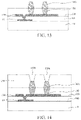
- FIG. 20-22 show top schematic views of metal probe structures in accordance with several embodiments of the present invention.
- FIG. 20 a top view of one of the metal probe structures shown in FIGS. 9 and 19 is shown.
- the metal probe C in the metal probe structure is composed of a metal layer 250 over a side and top surfaces of two metal stacks A/A′ and the two metal stacks A/A′, and the cross-sectional view shown in FIGS. 9 and 19 mainly show the cross-sectional view along the line F-F in FIG. 20 .
- FIG. 21 another top view of the metal probe structure shown in FIGS. 9 and 19 is shown.
- the metal probe C in the metal probe structure is composed of a metal layer 250 over a side and top surfaces of four metal stacks A/A′ and the four metal stacks A/A′, and the cross-sectional view shown in FIGS. 9 and 19 only partially show the cross-sectional view of the two metal stacks A/A′ along the line F-F in FIG. 21 .
- FIG. 22 shows another schematic diagram of the metal probe structure shown in FIGS. 9 and 19 .
- the metal probe C of the metal probe structure shown in FIGS. 9 and 19 may be composed only of the metal layer 250 over a side and top surfaces of a metal stack A/A′ and the metal stack A/A′, and the cross-sectional views shown in FIGS. 9 and 19 only partially show the profile of a metal stack A/A′ along the line F-F in FIG. 22 .
- the method for fabricating the metal probe structure of the present invention and the metal probe structure formed by thereof is a composite metal probe structure made of a plurality of metal components formed by stacking a plurality of metal components and a metal layer physically connecting the metal stacks.
- properties of the metal probe structure including but not limited to such as the material, the number of layers, the pitch, and the aspect ratio of the metal stack and the metal layer can be designed and adjusted according to the type of the test wafer, thereby providing a metal probe with good reliability, electrical conductivity, heat dissipation and/or mechanical strength than the metal probe used in the conventional probe card.
Landscapes
- Physics & Mathematics (AREA)
- General Physics & Mathematics (AREA)
- Engineering & Computer Science (AREA)
- Microelectronics & Electronic Packaging (AREA)
- Computer Hardware Design (AREA)
- General Engineering & Computer Science (AREA)
- Manufacturing & Machinery (AREA)
- Geometry (AREA)
- Measuring Leads Or Probes (AREA)
- Testing Or Measuring Of Semiconductors Or The Like (AREA)
- Testing Of Individual Semiconductor Devices (AREA)
Abstract
Description
Claims (18)
Applications Claiming Priority (2)
| Application Number | Priority Date | Filing Date | Title |
|---|---|---|---|
| TW108138660A TWI706139B (en) | 2019-10-25 | 2019-10-25 | Metal probe structure and method for fabricating the same |
| TW108138660 | 2019-10-25 |
Publications (2)
| Publication Number | Publication Date |
|---|---|
| US20210123949A1 US20210123949A1 (en) | 2021-04-29 |
| US11474128B2 true US11474128B2 (en) | 2022-10-18 |
Family
ID=69326356
Family Applications (1)
| Application Number | Title | Priority Date | Filing Date |
|---|---|---|---|
| US16/747,557 Active 2040-06-19 US11474128B2 (en) | 2019-10-25 | 2020-01-21 | Metal probe structure and method for fabricating the same |
Country Status (6)
| Country | Link |
|---|---|
| US (1) | US11474128B2 (en) |
| EP (1) | EP3812775B1 (en) |
| JP (1) | JP6999730B2 (en) |
| KR (1) | KR102358293B1 (en) |
| CN (1) | CN112710877A (en) |
| TW (1) | TWI706139B (en) |
Families Citing this family (2)
| Publication number | Priority date | Publication date | Assignee | Title |
|---|---|---|---|---|
| US11821918B1 (en) * | 2020-04-24 | 2023-11-21 | Microfabrica Inc. | Buckling beam probe arrays and methods for making such arrays including forming probes with lateral positions matching guide plate hole positions |
| TWI839966B (en) * | 2022-11-24 | 2024-04-21 | 漢民測試系統股份有限公司 | Probe card |
Citations (27)
| Publication number | Priority date | Publication date | Assignee | Title |
|---|---|---|---|---|
| JPS644042A (en) | 1987-06-09 | 1989-01-09 | Tektronix Inc | Prober |
| US20020005728A1 (en) * | 1999-04-15 | 2002-01-17 | Gordon M. Babson | Micro probe and method of fabricating same |
| US6476333B1 (en) * | 1993-11-16 | 2002-11-05 | Formfactor, Inc. | Raised contact structures (solder columns) |
| JP2004301527A (en) | 2003-03-28 | 2004-10-28 | Fujitsu Ltd | Probe card and method of manufacturing probe card |
| US20050093176A1 (en) | 2003-10-29 | 2005-05-05 | Meng-Chi Hung | Bonding pad structure |
| US20050269697A1 (en) | 2004-06-04 | 2005-12-08 | Seiko Epson Corporation | Semiconductor device, circuit board, and electronic instrument |
| JP2006507479A (en) | 2002-06-24 | 2006-03-02 | ナノネクサス インク | Structure and manufacturing process of probe card assembly and package with wafer level spring |
| JP2006078495A (en) | 2004-04-27 | 2006-03-23 | Jsr Corp | Sheet probe and its application |
| JP2006189430A (en) | 2004-12-31 | 2006-07-20 | Wen-Chang Dong | Thin-film circuit carrying micro machine probe and its manufacturing method and application therefor |
| US20060257631A1 (en) * | 2005-04-05 | 2006-11-16 | Chang Chi S | Probe pad structure in a ceramic space transformer |
| KR20070010187A (en) | 2004-04-27 | 2007-01-22 | 제이에스알 가부시끼가이샤 | Sheet-like probes, methods for their manufacture and uses thereof |
| TWI276805B (en) | 2005-11-10 | 2007-03-21 | Mjc Probe Inc | Probe of probe card and manufacturing method thereof |
| JP2008128882A (en) | 2006-11-22 | 2008-06-05 | Sumitomo Electric Ind Ltd | Contact probe and manufacturing method thereof |
| US20090051041A1 (en) * | 2007-08-24 | 2009-02-26 | Ngk Spark Plug Co., Ltd. | Multilayer wiring substrate and method for manufacturing the same, and substrate for use in ic inspection device and method for manufacturing the same |
| KR20100048673A (en) | 2008-10-31 | 2010-05-11 | 티에스씨멤시스(주) | Probe structure and method of manufacturing a probe structure |
| US20100176396A1 (en) | 2007-07-03 | 2010-07-15 | Advantest Corporation | Probe, probe card, and method of production of probe |
| US20120058653A1 (en) | 2009-06-29 | 2012-03-08 | Hsio Technologies, Llc | Singulated semiconductor device separable electrical interconnect |
| CN102384992A (en) * | 2011-07-12 | 2012-03-21 | 日月光半导体制造股份有限公司 | Probe card and manufacturing method thereof |
| KR20120031141A (en) | 2010-09-22 | 2012-03-30 | 팔로 알토 리서치 센터 인코포레이티드 | Microsprings at least partially embedded in a laminate structure and methods for producing same |
| CN102455373A (en) | 2010-10-19 | 2012-05-16 | 群成科技股份有限公司 | Probe card structure |
| US20120286817A1 (en) | 2011-05-09 | 2012-11-15 | Cascade Microtech, Inc. | Probe head assemblies, components thereof, test systems including the same, and methods of operating the same |
| US8485418B2 (en) | 1995-05-26 | 2013-07-16 | Formfactor, Inc. | Method of wirebonding that utilizes a gas flow within a capillary from which a wire is played out |
| US8849993B2 (en) | 2000-06-16 | 2014-09-30 | Intel Corporation | Method and apparatus for rate limiting |
| TWI489916B (en) | 2012-04-11 | 2015-06-21 | Nihon Micronics Kk | Multilayer wiring board and manufacturing method thereof |
| US20160091532A1 (en) | 2014-09-26 | 2016-03-31 | Qualcomm Incorporated | Flexible film electrical-test substrates with conductive coupling post(s) for integrated circuit (ic) bump(s) electrical testing, and related methods and testing apparatuses |
| TWI663406B (en) | 2016-05-31 | 2019-06-21 | 巨擘科技股份有限公司 | Probe card device |
| CN110136617A (en) | 2019-05-15 | 2019-08-16 | 业成科技(成都)有限公司 | Probe and preparation method thereof |
Family Cites Families (12)
| Publication number | Priority date | Publication date | Assignee | Title |
|---|---|---|---|---|
| GB1456994A (en) * | 1973-06-28 | 1976-12-01 | Marconi Co Ltd | Methods for forming electrical internconnection between metal layers for printed circuit assembly |
| JPS59153901A (en) * | 1983-02-21 | 1984-09-01 | Fuji Electric Co Ltd | Cooling device for rotor in steam turbine |
| JPH06347481A (en) * | 1993-06-11 | 1994-12-22 | Nitto Denko Corp | Probe structure |
| TW429575B (en) * | 1999-11-17 | 2001-04-11 | Taiwan Semiconductor Mfg | Structure and method for enhancing the hardness of Al pad |
| KR100376878B1 (en) * | 2000-08-09 | 2003-03-19 | 주식회사 하이닉스반도체 | Method for fabricating wafer level package |
| TWI320963B (en) * | 2006-12-06 | 2010-02-21 | Princo Corp | Method of manufacturing hybrid structure of multi-layer substrates and hybrid structure thereof |
| KR20090009664A (en) * | 2007-07-20 | 2009-01-23 | (주) 미코티엔 | A probe structure |
| TWI389290B (en) * | 2007-11-08 | 2013-03-11 | Ind Tech Res Inst | Chip structure and process thereof, stacked structure of chips and process thereof |
| JP5228207B2 (en) * | 2008-07-07 | 2013-07-03 | 山一電機株式会社 | Inspection probe |
| KR101766261B1 (en) * | 2015-08-05 | 2017-08-23 | (주)엠투엔 | Probe pin and method for manufacturing the same |
| IT201700051157A1 (en) * | 2017-05-11 | 2018-11-11 | Technoprobe Spa | Manufacturing method of a multilayer of a measurement card for an electronic device test device |
| KR101990458B1 (en) * | 2018-03-27 | 2019-06-18 | (주)티에스이 | Probe card and method for manufacturing the same |
-
2019
- 2019-10-25 TW TW108138660A patent/TWI706139B/en active
-
2020
- 2020-01-21 US US16/747,557 patent/US11474128B2/en active Active
- 2020-01-27 EP EP20153763.6A patent/EP3812775B1/en active Active
- 2020-02-24 CN CN202010113578.3A patent/CN112710877A/en active Pending
- 2020-03-30 JP JP2020061236A patent/JP6999730B2/en active Active
- 2020-05-29 KR KR1020200064998A patent/KR102358293B1/en active Active
Patent Citations (37)
| Publication number | Priority date | Publication date | Assignee | Title |
|---|---|---|---|---|
| US4912399A (en) | 1987-06-09 | 1990-03-27 | Tektronix, Inc. | Multiple lead probe for integrated circuits in wafer form |
| JPS644042A (en) | 1987-06-09 | 1989-01-09 | Tektronix Inc | Prober |
| JP2007173846A (en) | 1993-11-16 | 2007-07-05 | Formfactor Inc | Semiconductor package assembly |
| US6476333B1 (en) * | 1993-11-16 | 2002-11-05 | Formfactor, Inc. | Raised contact structures (solder columns) |
| US8485418B2 (en) | 1995-05-26 | 2013-07-16 | Formfactor, Inc. | Method of wirebonding that utilizes a gas flow within a capillary from which a wire is played out |
| US20020005728A1 (en) * | 1999-04-15 | 2002-01-17 | Gordon M. Babson | Micro probe and method of fabricating same |
| US8849993B2 (en) | 2000-06-16 | 2014-09-30 | Intel Corporation | Method and apparatus for rate limiting |
| JP2006507479A (en) | 2002-06-24 | 2006-03-02 | ナノネクサス インク | Structure and manufacturing process of probe card assembly and package with wafer level spring |
| JP2004301527A (en) | 2003-03-28 | 2004-10-28 | Fujitsu Ltd | Probe card and method of manufacturing probe card |
| US20050093176A1 (en) | 2003-10-29 | 2005-05-05 | Meng-Chi Hung | Bonding pad structure |
| US20070200574A1 (en) | 2004-04-27 | 2007-08-30 | Jsr Corporation | Sheet-like probe, method of producing the probe, and application of the probe |
| KR20070010187A (en) | 2004-04-27 | 2007-01-22 | 제이에스알 가부시끼가이샤 | Sheet-like probes, methods for their manufacture and uses thereof |
| JP2006078495A (en) | 2004-04-27 | 2006-03-23 | Jsr Corp | Sheet probe and its application |
| US7737707B2 (en) | 2004-04-27 | 2010-06-15 | Jsr Corporation | Sheet-like probe, method of producing the probe, and application of the probe |
| US20050269697A1 (en) | 2004-06-04 | 2005-12-08 | Seiko Epson Corporation | Semiconductor device, circuit board, and electronic instrument |
| JP2006189430A (en) | 2004-12-31 | 2006-07-20 | Wen-Chang Dong | Thin-film circuit carrying micro machine probe and its manufacturing method and application therefor |
| US7388388B2 (en) | 2004-12-31 | 2008-06-17 | Wen-Chang Dong | Thin film with MEMS probe circuits and MEMS thin film probe head using the same |
| US20060257631A1 (en) * | 2005-04-05 | 2006-11-16 | Chang Chi S | Probe pad structure in a ceramic space transformer |
| TWI276805B (en) | 2005-11-10 | 2007-03-21 | Mjc Probe Inc | Probe of probe card and manufacturing method thereof |
| US20070103177A1 (en) | 2005-11-10 | 2007-05-10 | Mjc Probe Incorporation | Probes of probe card and the method of making the same |
| JP2008128882A (en) | 2006-11-22 | 2008-06-05 | Sumitomo Electric Ind Ltd | Contact probe and manufacturing method thereof |
| TWI393890B (en) | 2007-07-03 | 2013-04-21 | Advantest Corp | Probe, probe card and probe manufacturing method |
| US20100176396A1 (en) | 2007-07-03 | 2010-07-15 | Advantest Corporation | Probe, probe card, and method of production of probe |
| US20090051041A1 (en) * | 2007-08-24 | 2009-02-26 | Ngk Spark Plug Co., Ltd. | Multilayer wiring substrate and method for manufacturing the same, and substrate for use in ic inspection device and method for manufacturing the same |
| KR20100048673A (en) | 2008-10-31 | 2010-05-11 | 티에스씨멤시스(주) | Probe structure and method of manufacturing a probe structure |
| US20120058653A1 (en) | 2009-06-29 | 2012-03-08 | Hsio Technologies, Llc | Singulated semiconductor device separable electrical interconnect |
| KR20120031141A (en) | 2010-09-22 | 2012-03-30 | 팔로 알토 리서치 센터 인코포레이티드 | Microsprings at least partially embedded in a laminate structure and methods for producing same |
| US8519534B2 (en) | 2010-09-22 | 2013-08-27 | Palo Alto Research Center Incorporated | Microsprings partially embedded in a laminate structure and methods for producing same |
| CN102455373A (en) | 2010-10-19 | 2012-05-16 | 群成科技股份有限公司 | Probe card structure |
| US20120286817A1 (en) | 2011-05-09 | 2012-11-15 | Cascade Microtech, Inc. | Probe head assemblies, components thereof, test systems including the same, and methods of operating the same |
| CN102384992A (en) * | 2011-07-12 | 2012-03-21 | 日月光半导体制造股份有限公司 | Probe card and manufacturing method thereof |
| TWI489916B (en) | 2012-04-11 | 2015-06-21 | Nihon Micronics Kk | Multilayer wiring board and manufacturing method thereof |
| US9622344B2 (en) | 2012-04-11 | 2017-04-11 | Kabushiki Kaisha Nihon Micronics | Multilayer wiring board with enclosed Ur-variant dual conductive layer |
| US20160091532A1 (en) | 2014-09-26 | 2016-03-31 | Qualcomm Incorporated | Flexible film electrical-test substrates with conductive coupling post(s) for integrated circuit (ic) bump(s) electrical testing, and related methods and testing apparatuses |
| TWI663406B (en) | 2016-05-31 | 2019-06-21 | 巨擘科技股份有限公司 | Probe card device |
| US10451654B2 (en) | 2016-05-31 | 2019-10-22 | Princo Corp. | Probe card device |
| CN110136617A (en) | 2019-05-15 | 2019-08-16 | 业成科技(成都)有限公司 | Probe and preparation method thereof |
Non-Patent Citations (1)
| Title |
|---|
| English Machine Translation of Chen et al. CN 102384992 (Chen) (Year: 2012). * |
Also Published As
| Publication number | Publication date |
|---|---|
| CN112710877A (en) | 2021-04-27 |
| TW202117331A (en) | 2021-05-01 |
| KR102358293B1 (en) | 2022-02-04 |
| JP2021067666A (en) | 2021-04-30 |
| US20210123949A1 (en) | 2021-04-29 |
| EP3812775B1 (en) | 2025-07-16 |
| JP6999730B2 (en) | 2022-01-19 |
| EP3812775A1 (en) | 2021-04-28 |
| TWI706139B (en) | 2020-10-01 |
| KR20210050425A (en) | 2021-05-07 |
Similar Documents
| Publication | Publication Date | Title |
|---|---|---|
| KR101962644B1 (en) | A test probe and test device using the same | |
| JP6614212B2 (en) | Wiring structure | |
| US8378704B2 (en) | Substrate for a probe card assembly | |
| CN101673694A (en) | Method for manufacturing space transformer of semiconductor test probe card | |
| JP2003207523A (en) | Contactor, its manufacturing method and contact method | |
| US7498252B2 (en) | Dual layer dielectric stack for microelectronics having thick metal lines | |
| US20210199696A1 (en) | Method of manufacturing probe card and probe card manufactured using same | |
| US11474128B2 (en) | Metal probe structure and method for fabricating the same | |
| US20190148325A1 (en) | Electronic device and method for manufacturing the same | |
| CN100477192C (en) | Semiconductor device and manufacturing method thereof | |
| US7679386B2 (en) | Probe card including contactors formed projection portion | |
| US7759165B1 (en) | Nanospring | |
| JP5449719B2 (en) | WIRING BOARD, IC ELECTRIC CHARACTERISTIC TESTING WIRING BOARD AND WIRING BOARD MANUFACTURING METHOD | |
| Ho et al. | Polymer-based fine pitch Cu RDL to enable cost-effective re-routing for 2.5 D interposer and 3D-IC | |
| US20230213555A1 (en) | Testing substrate and manufacturing method thereof and probe card | |
| US8237450B2 (en) | Method of testing insulation property of wafer-level chip scale package and TEG pattern used in the method | |
| CN223181138U (en) | Passive devices on semiconductor substrates and semiconductor devices | |
| TWI803086B (en) | Probe card assembly | |
| JP2012253189A (en) | Method for manufacturing semiconductor device and semiconductor device | |
| Duval et al. | Semi-additive Cu-polymer RDL process for interposers applications | |
| TWI271528B (en) | Method of circuit electrical test | |
| JP2013108993A (en) | Wiring board, wiring board for ic electrical characteristics test, and method of manufacturing wiring board |
Legal Events
| Date | Code | Title | Description |
|---|---|---|---|
| AS | Assignment |
Owner name: PRINCO CORP., TAIWAN Free format text: ASSIGNMENT OF ASSIGNORS INTEREST;ASSIGNORS:CHU, YI-LIN;KU, HUNG- SHENG;REEL/FRAME:051560/0915 Effective date: 20191211 |
|
| FEPP | Fee payment procedure |
Free format text: ENTITY STATUS SET TO UNDISCOUNTED (ORIGINAL EVENT CODE: BIG.); ENTITY STATUS OF PATENT OWNER: LARGE ENTITY |
|
| STPP | Information on status: patent application and granting procedure in general |
Free format text: DOCKETED NEW CASE - READY FOR EXAMINATION |
|
| STPP | Information on status: patent application and granting procedure in general |
Free format text: NON FINAL ACTION MAILED |
|
| STPP | Information on status: patent application and granting procedure in general |
Free format text: RESPONSE TO NON-FINAL OFFICE ACTION ENTERED AND FORWARDED TO EXAMINER |
|
| STPP | Information on status: patent application and granting procedure in general |
Free format text: FINAL REJECTION MAILED |
|
| STPP | Information on status: patent application and granting procedure in general |
Free format text: DOCKETED NEW CASE - READY FOR EXAMINATION |
|
| STPP | Information on status: patent application and granting procedure in general |
Free format text: NON FINAL ACTION MAILED |
|
| STPP | Information on status: patent application and granting procedure in general |
Free format text: RESPONSE TO NON-FINAL OFFICE ACTION ENTERED AND FORWARDED TO EXAMINER |
|
| STPP | Information on status: patent application and granting procedure in general |
Free format text: NOTICE OF ALLOWANCE MAILED -- APPLICATION RECEIVED IN OFFICE OF PUBLICATIONS |
|
| STPP | Information on status: patent application and granting procedure in general |
Free format text: PUBLICATIONS -- ISSUE FEE PAYMENT VERIFIED |
|
| STCF | Information on status: patent grant |
Free format text: PATENTED CASE |