US11471997B2 - Polishing pad, polishing apparatus and a method for polishing silicon wafer - Google Patents
Polishing pad, polishing apparatus and a method for polishing silicon wafer Download PDFInfo
- Publication number
- US11471997B2 US11471997B2 US17/136,544 US202017136544A US11471997B2 US 11471997 B2 US11471997 B2 US 11471997B2 US 202017136544 A US202017136544 A US 202017136544A US 11471997 B2 US11471997 B2 US 11471997B2
- Authority
- US
- United States
- Prior art keywords
- polishing
- silicon wafer
- annular groove
- edge
- polishing pad
- Prior art date
- Legal status (The legal status is an assumption and is not a legal conclusion. Google has not performed a legal analysis and makes no representation as to the accuracy of the status listed.)
- Active
Links
- 238000005498 polishing Methods 0.000 title claims abstract description 209
- XUIMIQQOPSSXEZ-UHFFFAOYSA-N Silicon Chemical compound [Si] XUIMIQQOPSSXEZ-UHFFFAOYSA-N 0.000 title claims abstract description 140
- 229910052710 silicon Inorganic materials 0.000 title claims abstract description 140
- 239000010703 silicon Substances 0.000 title claims abstract description 140
- 238000000034 method Methods 0.000 title abstract description 20
- 238000004519 manufacturing process Methods 0.000 abstract description 8
- 230000033001 locomotion Effects 0.000 description 13
- 239000007788 liquid Substances 0.000 description 10
- 238000007517 polishing process Methods 0.000 description 7
- 238000005516 engineering process Methods 0.000 description 2
- 238000012986 modification Methods 0.000 description 2
- 230000004048 modification Effects 0.000 description 2
- 239000004065 semiconductor Substances 0.000 description 2
- 238000011161 development Methods 0.000 description 1
- 230000018109 developmental process Effects 0.000 description 1
- 230000000694 effects Effects 0.000 description 1
- 238000007518 final polishing process Methods 0.000 description 1
- 229910021421 monocrystalline silicon Inorganic materials 0.000 description 1
- 229910052594 sapphire Inorganic materials 0.000 description 1
- 239000010980 sapphire Substances 0.000 description 1
- 238000004062 sedimentation Methods 0.000 description 1
- HBMJWWWQQXIZIP-UHFFFAOYSA-N silicon carbide Chemical compound [Si+]#[C-] HBMJWWWQQXIZIP-UHFFFAOYSA-N 0.000 description 1
- 229910010271 silicon carbide Inorganic materials 0.000 description 1
- 230000003068 static effect Effects 0.000 description 1
Images


Classifications
-
- B—PERFORMING OPERATIONS; TRANSPORTING
- B24—GRINDING; POLISHING
- B24B—MACHINES, DEVICES, OR PROCESSES FOR GRINDING OR POLISHING; DRESSING OR CONDITIONING OF ABRADING SURFACES; FEEDING OF GRINDING, POLISHING, OR LAPPING AGENTS
- B24B29/00—Machines or devices for polishing surfaces on work by means of tools made of soft or flexible material with or without the application of solid or liquid polishing agents
- B24B29/02—Machines or devices for polishing surfaces on work by means of tools made of soft or flexible material with or without the application of solid or liquid polishing agents designed for particular workpieces
-
- B—PERFORMING OPERATIONS; TRANSPORTING
- B24—GRINDING; POLISHING
- B24B—MACHINES, DEVICES, OR PROCESSES FOR GRINDING OR POLISHING; DRESSING OR CONDITIONING OF ABRADING SURFACES; FEEDING OF GRINDING, POLISHING, OR LAPPING AGENTS
- B24B37/00—Lapping machines or devices; Accessories
- B24B37/04—Lapping machines or devices; Accessories designed for working plane surfaces
- B24B37/042—Lapping machines or devices; Accessories designed for working plane surfaces operating processes therefor
-
- B—PERFORMING OPERATIONS; TRANSPORTING
- B24—GRINDING; POLISHING
- B24B—MACHINES, DEVICES, OR PROCESSES FOR GRINDING OR POLISHING; DRESSING OR CONDITIONING OF ABRADING SURFACES; FEEDING OF GRINDING, POLISHING, OR LAPPING AGENTS
- B24B37/00—Lapping machines or devices; Accessories
- B24B37/005—Control means for lapping machines or devices
-
- B—PERFORMING OPERATIONS; TRANSPORTING
- B24—GRINDING; POLISHING
- B24B—MACHINES, DEVICES, OR PROCESSES FOR GRINDING OR POLISHING; DRESSING OR CONDITIONING OF ABRADING SURFACES; FEEDING OF GRINDING, POLISHING, OR LAPPING AGENTS
- B24B37/00—Lapping machines or devices; Accessories
- B24B37/04—Lapping machines or devices; Accessories designed for working plane surfaces
-
- B—PERFORMING OPERATIONS; TRANSPORTING
- B24—GRINDING; POLISHING
- B24B—MACHINES, DEVICES, OR PROCESSES FOR GRINDING OR POLISHING; DRESSING OR CONDITIONING OF ABRADING SURFACES; FEEDING OF GRINDING, POLISHING, OR LAPPING AGENTS
- B24B37/00—Lapping machines or devices; Accessories
- B24B37/11—Lapping tools
- B24B37/20—Lapping pads for working plane surfaces
- B24B37/26—Lapping pads for working plane surfaces characterised by the shape of the lapping pad surface, e.g. grooved
-
- B—PERFORMING OPERATIONS; TRANSPORTING
- B24—GRINDING; POLISHING
- B24D—TOOLS FOR GRINDING, BUFFING OR SHARPENING
- B24D13/00—Wheels having flexibly-acting working parts, e.g. buffing wheels; Mountings therefor
- B24D13/14—Wheels having flexibly-acting working parts, e.g. buffing wheels; Mountings therefor acting by the front face
-
- H—ELECTRICITY
- H01—ELECTRIC ELEMENTS
- H01L—SEMICONDUCTOR DEVICES NOT COVERED BY CLASS H10
- H01L21/00—Processes or apparatus adapted for the manufacture or treatment of semiconductor or solid state devices or of parts thereof
- H01L21/02—Manufacture or treatment of semiconductor devices or of parts thereof
- H01L21/02002—Preparing wafers
- H01L21/02005—Preparing bulk and homogeneous wafers
- H01L21/02008—Multistep processes
- H01L21/0201—Specific process step
- H01L21/02024—Mirror polishing
-
- H—ELECTRICITY
- H01—ELECTRIC ELEMENTS
- H01L—SEMICONDUCTOR DEVICES NOT COVERED BY CLASS H10
- H01L21/00—Processes or apparatus adapted for the manufacture or treatment of semiconductor or solid state devices or of parts thereof
- H01L21/02—Manufacture or treatment of semiconductor devices or of parts thereof
- H01L21/04—Manufacture or treatment of semiconductor devices or of parts thereof the devices having potential barriers, e.g. a PN junction, depletion layer or carrier concentration layer
- H01L21/18—Manufacture or treatment of semiconductor devices or of parts thereof the devices having potential barriers, e.g. a PN junction, depletion layer or carrier concentration layer the devices having semiconductor bodies comprising elements of Group IV of the Periodic Table or AIIIBV compounds with or without impurities, e.g. doping materials
- H01L21/30—Treatment of semiconductor bodies using processes or apparatus not provided for in groups H01L21/20 - H01L21/26
- H01L21/302—Treatment of semiconductor bodies using processes or apparatus not provided for in groups H01L21/20 - H01L21/26 to change their surface-physical characteristics or shape, e.g. etching, polishing, cutting
- H01L21/306—Chemical or electrical treatment, e.g. electrolytic etching
- H01L21/30625—With simultaneous mechanical treatment, e.g. mechanico-chemical polishing
-
- H—ELECTRICITY
- H01—ELECTRIC ELEMENTS
- H01L—SEMICONDUCTOR DEVICES NOT COVERED BY CLASS H10
- H01L21/00—Processes or apparatus adapted for the manufacture or treatment of semiconductor or solid state devices or of parts thereof
- H01L21/67—Apparatus specially adapted for handling semiconductor or electric solid state devices during manufacture or treatment thereof; Apparatus specially adapted for handling wafers during manufacture or treatment of semiconductor or electric solid state devices or components ; Apparatus not specifically provided for elsewhere
- H01L21/67005—Apparatus not specifically provided for elsewhere
- H01L21/67011—Apparatus for manufacture or treatment
- H01L21/67092—Apparatus for mechanical treatment
Definitions
- the present invention relates to a semiconductor manufacture, in particular to a polishing pad, a polishing apparatus and a method for polishing silicon wafer.
- the silicon wafer is subjected to double side polish (DSP) and final polish (FP).
- DSP double side polish
- FP final polish
- DSP is used to polish the front side and back side of the wafer, and control the shape of the wafer by polishing disc.
- FP is used to polish the front side of the wafer.
- the polishing liquid easily accumulates at the edge, causing the thinner edge of the wafer.
- the conventional apparatus and the conventional process are unable to precisely regulate the polishing at the edge position of 145 mm ⁇ 149 mm of the silicon wafer, especially when the polishing rate for entire wafer has to be maintained. Reduction of polishing rate at the wafer edge cannot be achieved by adjusting the conventional process parameters.
- the present application provides a polishing pad for polishing a silicon wafer.
- the polishing pad has a polishing surface contacting to the silicon wafer.
- the polishing surface is provided with at least one groove. During the polishing, at least partial edge of the silicon wafer suspends above the groove.
- the groove comprises a first annular groove near the pad edge and a second annular groove near the pad center.
- the silicon wafer has a diameter larger than a distance between the inner edge of the first annular groove and the outer edge of the second annular groove, and less than or equal to a distance between the outer edge of the first annular groove and the inner edge of the second annular groove.
- the polishing pad, the first annular groove and the second annular groove are concentric.
- the first annular groove has a width of 3 mm ⁇ 8 mm, a depth of 0.5 mm ⁇ 2 mm, an outer edge radius of 335 mm ⁇ 340 mm, and an inner edge radius of 330 mm ⁇ 335 mm.
- the second annular groove has a width of 3 mm ⁇ ⁇ 8 mm, a depth of 0.5 mm ⁇ 2 mm, an outer edge radius of 35 mm ⁇ 45 mm, and an inner edge radius of 30 mm ⁇ 40 mm.
- the present application also provides a polishing apparatus for polishing a silicon wafer comprising: a polishing pad as described above; a driving device for driving the polishing pad disposed thereon to rotate; a polishing head for fixing the silicon wafer to contact the front side of the silicon wafer with the polishing pad and suspend the edge of the silicon wafer above the groove of the polishing pad.
- the present application further provides a process for polishing a silicon wafer, comprising: fixing a silicon wafer by a polishing head; contacting the front side of the silicon wafer to a polishing surface of a polishing pad driven by the polishing head, wherein an edge of the silicon wafer suspends above a groove of the polishing surface of the polishing pad; driving the polishing head and the polishing pad to rotate to polish the front side of the silicon wafer.
- the polishing head and the polishing pad rotate with same direction.
- the process further comprises: adjusting the contact area of the edge of the silicon wafer to the groove by controlling the motion of polishing head, and thereby adjusting the polishing rate to the edge of the silicon wafer.
- the step of controlling the motion of polishing head comprises: controlling the polishing head to conduct reciprocating motion along with a radius direction of the polishing pad.
- the polishing pad, the polishing apparatus and the polishing method for silicon wafer can reduce the polishing rate at the edge of the silicon wafer while keeping the polishing rate of the entire wafer basically unchanged, thereby improving the flatness of the edge thickness of the silicon wafer as well as improving the production yield.
- the present application also provides a process.
- FIG. 1 shows a schematic view of a structure of a polishing pad in accordance with one embodiment of the present application.
- FIG. 2 shows a schematic view of a silicon wafer polished by a polishing pad in accordance with one embodiment of the present application.
- FIG. 3 shows a sectional view of a polishing pad and a silicon wafer in accordance with one embodiment of the present application.
- FIG. 4 shows a schematic view of groove size of a polishing pad in accordance with one embodiment of the present application.
- FIG. 5 shows a schematic view of a motion track of a groove relative to a silicon wafer edge during the polishing process in accordance with one embodiment of the present application.
- FIG. 6 shows a schematic view of a structure of a polishing apparatus in accordance with one embodiment of the present application.
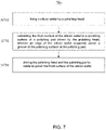
- FIG. 7 shows a flow chart of a method for polishing silicon wafer in accordance with one embodiment of the present application.
- FIG. 8 shows a schematic view of motion of a polishing head during the polishing process in accordance with one embodiment of the present application.
- FIG. 9 shows a relationship between a removed thickness and a wafer radius with various entry sizes of wafer edge into the groove.
- Example embodiments are provided so that this disclosure will be thorough, and will fully convey the scope to those who are skilled in the art. Numerous specific details are set forth such as examples of specific components, devices, and methods, to provide a thorough understanding of embodiments of the present disclosure. It will be apparent to those skilled in the art that specific details need not be employed, that example embodiments may be embodied in many different forms and that neither should be construed to limit the scope of the disclosure. In some example embodiments, well-known processes, well-known device structures, and well-known technologies are not described in detail.
- the present application provides a polishing pad for polishing a silicon wafer.
- the polishing pad has a polishing surface contacting to the silicon wafer.
- the polishing surface is provided with at least one groove. During the polishing, at least partial edge of the silicon wafer suspends above the groove.
- the present application provides a polishing apparatus for polishing a silicon wafer comprising: a polishing pad as described in the above embodiments; a driving device for driving the polishing pad disposed thereon to rotate; a polishing head for fixing the silicon wafer to contact the front side of the silicon wafer with the polishing pad and suspend the edge of the silicon wafer above the groove of the polishing pad.
- the present application further provides a process for polishing a silicon wafer, comprising: fixing a silicon wafer by a polishing head; contacting the front side of the silicon wafer to a polishing surface of a polishing pad driven by the polishing head, wherein an edge of the silicon wafer suspends above a groove of the polishing surface of the polishing pad; driving the polishing head and the polishing pad to rotate to polish the front side of the silicon wafer
- the polishing pad, the polishing apparatus and the polishing method for silicon wafer of the present application can reduce the polishing rate at the edge of the silicon wafer while keeping the polishing rate of the entire wafer basically unchanged, thereby improving the flatness of the edge thickness of the silicon wafer as well as improving the production yield.
- FIGS. 1-5 Example embodiments of the polishing pad will now be described more fully with reference to the accompanying drawings FIGS. 1-5 .
- the polishing pad 100 can be a circular polishing pad, the polishing surface is provided with grooves.
- the grooves can include the first annular groove 101 near the pad edge and a second annular groove 102 near the pad center.
- the polishing surface between the first annular groove 101 and the second annular groove 102 can be plane.
- the first annular groove 101 and the second annular groove 102 are concentric.
- the sectional shape of the first annular groove 101 and the second annular groove 102 can include, but not be limited to, rectangle.
- the distance between the inner edge of the first annular groove 101 and the outer edge of the second annular groove 102 is smaller than the diameter of the silicon wafer.
- the distance between the outer edge of the first annular groove 101 and the inner edge of the second annular groove 102 is larger than or equal to the diameter of the silicon wafer.
- the width of the edge of the silicon wafer 200 suspended above the first annular groove 101 is basically same to that above the second annular groove 102 .
- the silicon wafer can be processed by DSP.
- the silicon wafer is semiconductor silicon wafer, which can include, but not be limited to, monocrystalline silicon wafer, sapphire silicon wafer, silicon carbide wafer and the like.
- the polishing pad 100 which improves polishing effects at the position 145-149 mm of the wafer edge are provided as follows.
- the first annular groove 101 has a width D 1 of 3 mm ⁇ 8 mm, such as 5 mm, a depth H 1 of 0.5 mm ⁇ 2 mm.
- Its inner edge, i.e. the inner circle close to the pad center has a radius of 330 mm ⁇ 335 mm, such as 334 mm.
- the width and depth of the second annular groove 102 can be identical or similar to that of the first annular groove 101 , i.e. the second annular groove 102 has a width D 2 of 3 mm ⁇ 8 mm, such as 5 mm, a depth H 2 of 0.5 mm ⁇ 2 mm.
- Its inner edge, i.e. the inner circle close to the pad center has a radius of 30 mm ⁇ 40 mm, such as 35 mm.
- the distance between the outer edge of the first annular groove 101 and the inner edge of the second annular groove 102 is larger than or equal to the diameter of the silicon wafer. While the silicon wafer is disposed between the first annular groove 101 and the second annular groove 102 , both of the first annular groove 101 and the second annular groove 102 are located below the silicon wafer 200 and some parts of the grooves are beyond the silicon wafer 200 . Accordingly, in the polishing process, the contact area between the silicon wafer 200 and the grooves can be adjusted by moving the silicon wafer 200 toward right or left along with the radius direction of the polishing pad 100 , thereby the polishing rate to the silicon wafer 200 can be adjusted.
- the distance D 3 between the outer edge of the first annular groove 101 and the edge of the silicon wafer 200 and the distance D 6 between the inner edge of the second annular groove 102 and the edge of the silicon wafer 200 can be 1 mm ⁇ 2 mm.
- the distance D 4 between the inner edge of the first annular groove 101 and the edge of the silicon wafer 200 and the distance D 5 between the outer edge of the second annular groove 102 and the edge of the silicon wafer 200 can be 2 mm ⁇ 3 mm
- the width of the silicon wafer 200 contacting with the groove is 2 mm ⁇ 3 mm and the amplitude of the left and right movement can be 2 mm ⁇ 4 mm.
- polishing pad 100 some parameters of the polishing pad 100 are provided herein, but the parameters of the pad are not limited accordingly. A person having ordinary skills in the art is able to adjust them based on the size of the silicon wafer or other requirements.
- FIG. 5 shows a schematic view of a motion track of the groove of the pad relative to the edge of the silicon wafer 200 during the polishing process in accordance with one embodiment of the present application.
- the polishing head drives the silicon wafer 200 to rotate in same direction. If the silicon wafer 200 is determined as static state, it observes that the polishing pad 100 rotates around the center of the silicon wafer 200 . Namely, the first annular groove 101 and the second annular groove 102 on the polishing pad 100 rotate around the center of the silicon wafer 200 , therefore, the motion track as shown in FIG. 5 is formed.
- FIG. 5 shows a schematic view of a motion track of the groove of the pad relative to the edge of the silicon wafer 200 during the polishing process in accordance with one embodiment of the present application.
- the area defined by the two dotted lines of the silicon wafer 200 is the edge area passing through the grooves, and its width can be D 4 or D 5 shown in FIG. 4 . Comparing with the remaining area except the edge of the silicon wafer, the existence of the first annular groove and the second annular groove reduces the contact area and the contact time between the edge of the silicon wafer and the polishing pad.
- the polishing head drives the silicon wafer 200 to rotate. Even if the polishing pad 100 merely has the first annular groove 101 or the second annular groove 102 , the groove is able to pass through every position at the edge of the silicon wafer 200 . In some embodiments, polishing pad 100 can be provided with only the first annular groove 101 or only the second annular groove 102 .
- the polishing pad 100 is further provided with one or plural drainage groove 103 .
- the drainage groove 103 connects the groove and the edge of the polishing pad 100 to remove the polishing liquid from the groove. As shown in FIG. 1 , the drainage groove 103 connects the second annular groove 102 by one terminal, passes through the first annular groove 101 , and connects to the edge of the polishing pad 100 by another terminal.
- the drainage groove 103 is able to drain the polishing liquid from the first annular groove 101 and the second annular groove 102 during the rotation of the polishing pad 100 . It prevent from the surface damages of the silicon wafer caused by sedimentation of the polishing liquid and debris.
- the drainage groove 103 is arch.
- the arch protrudes toward the rotation direction of the polishing pad, so that it is facilitate to drain the polishing liquid from the grooves by the centrifugal force from the rotation of the polishing pad 100 .
- the drainage groove 103 can be tangent with the outer edge of the second annular groove 102 .
- the drainage groove 103 has a depth not less than the depth of the first annular groove 101 or the second annular groove 102 , so that the polishing liquid flows easily from the first annular groove 101 and the second annular groove 102 to the drainage groove 103 .
- the drainage groove 103 can be symmetrically disposed around the circle of the polishing pad 100 .
- the depth of the drainage groove 103 can be uniformly distributed.
- the depth of the drainage groove 103 can gradually increase from the center to the edge of the polishing pad 100 .
- the drainage groove 103 can start from the second annular groove 102 , passing through the first annular groove 101 , and extend to the edge of polishing pad 100 .
- the drainage groove connecting the second annular groove 102 and the first annular groove 101 can be disposed independently from the drainage groove connecting the first annular groove 101 and the edge of the polishing pad 100 , and the numbers of the two kinds of the drainage groove can be same or different, so long as the polishing liquid can be removed from the first annular groove 101 and the second annular groove 102 .
- the number is not limited therein.
- a person having ordinary skills in the art is able to adjust and modify the drainage groove's number, width, depth, radian and the like according to flow rate of polishing liquid, rotation rate of polishing pad, size of the first annular groove 101 and the second annular groove 102 to effectively drain the polishing liquid from the first annular groove 101 and the second annular groove 102 .
- the polishing pad of the present application can reduce the polishing rate at the edge of the silicon wafer while keeping the polishing rate of the entire wafer basically unchanged, thereby improving the flatness of the edge thickness of the silicon wafer as well as improving the production yield.
- the polishing apparatus comprises a polishing pad 100 , a driving device 400 and a polishing head 300 .
- the polishing pad 100 can be any polishing pad as described above, i.e. the polishing pad 100 having a polishing surface with at least one groove, and at least partial edge of the silicon wafer hangs above the groove during polishing.
- the polishing pad 100 is disposed on the driving device 400 , and is driven by the driving device 400 to rotate.
- the polishing head 300 is used to fix the silicon wafer to contact the front side of the silicon wafer with the polishing pad 100 and suspend the edge of the silicon wafer above the groove of the polishing pad 100 .
- the driving device 400 can be a big turntable disposed below the polishing pad 100 , and drives the polishing pad 100 to rotate clockwise or counterclockwise.
- the polishing head 300 is disposed above the polishing pad 100 for carrying the silicon wafer.
- the polishing head 300 comprises a base, a backing and a fixing part.
- a chamber between the base and the backing is evacuated to suck the silicon wafer.
- the polishing head 300 applies a force to the back side of the silicon wafer and drives the silicon wafer to rotate with a certain speed.
- the rotation direction of the silicon wafer can be same to that of the polishing pad 100 .
- a supply port can be disposed above the polishing pad to supply the polishing liquid to the polishing pad.
- the polishing pad having a groove correspondent to the edge of the silicon wafer is provided.
- the above polishing pad can be applied with the conventional polishing apparatus. Accordingly, the polishing apparatus according to the present invention can reduce the polishing rate at the edge of the silicon wafer while keeping the polishing rate of the entire wafer basically unchanged, thereby improving the flatness of the edge thickness of the silicon wafer as well as improving the production yield.
- the polishing method comprises the following steps.
- Step S 710 fixing a silicon wafer by a polishing head.
- the silicon wafer can be processed by DSP.
- the polishing head can suck the silicon wafer via evacuation.
- Step S 720 contacting the front surface of the silicon wafer to a polishing surface of a polishing pad driven by the polishing head, wherein an edge of the silicon wafer hangs above a groove of the polishing surface of the polishing pad.
- the polishing surface of the polishing pad is provided with a first annular groove near the pad edge and/or a second annular groove near the pad center.
- the polishing head can drive the silicon wafer and fix the silicon wafer between the first annular groove and the second annular groove.
- the two opposite edges at the same diameter of the silicon wafer respectively suspend above the first annular groove and the second annular groove.
- a certain area of the edge of the silicon wafer suspends above the first annular groove and the second annular groove, and does not contact with the polishing pad.
- a distance between the outer edge of the first annular groove and the inner edge of the second annular groove is larger than the diameter of the silicon wafer, thereby a certain space is maintained for the left and right motion of the silicon wafer.
- the structure of the polishing pad and the location relationship between the silicon wafer and the polishing pad can be referred the above descriptions.
- Step S 730 driving the polishing head and the polishing pad to rotate to polish the front side of the silicon wafer.
- the polishing head applies a force to the back side of the silicon wafer and drives the silicon wafer to rotate with a certain speed.
- the rotation direction of the silicon wafer can be same to that of the polishing pad, i.e. both are clockwise or both are counterclockwise.
- the edge of the silicon wafer continuously passes through the first annular groove and the second annular groove, causing reduction of contact time and area between the polishing pad and the edge of the silicon wafer. Accordingly, the polishing rate at the edge of the silicon wafer can be reduced while keeping the polishing rate of the entire wafer basically unchanged, thereby improving the flatness of the edge thickness of the silicon wafer as well as improving the production yield.
- the polishing head in addition to rotation and applying force, is able to adjust the area of the silicon wafer suspending above the grooves by its motion.
- the polishing rate at the edge of the silicon wafer can be adjusted thereby.
- the motion of the polishing head is reciprocating motion. It can be understood that, the width of the edge of the silicon wafer suspending above the groove is larger while the amplitude of the left and right movement is larger.
- FIG. 9 shows a relationship between a removed thickness and a silicon wafer radius with the sizes of 0, 2 mm and 4 mm of the wafer edge suspending above groove. It can be observed from FIG. 9 that, while the contact width of the wafer edge is larger, the relative removed thickness at the wafer edge (the position at the radius 145 mm ⁇ 149 mm) is smaller, i.e. the polishing rate at the edge of the silicon wafer is slower.
- the polishing rate at the edge of the silicon wafer can be reduced while keeping the polishing rate of the entire wafer basically unchanged, thereby improving the flatness of the edge thickness of the silicon wafer as well as improving the production yield.
Landscapes
- Engineering & Computer Science (AREA)
- Mechanical Engineering (AREA)
- Physics & Mathematics (AREA)
- Condensed Matter Physics & Semiconductors (AREA)
- General Physics & Mathematics (AREA)
- Manufacturing & Machinery (AREA)
- Computer Hardware Design (AREA)
- Microelectronics & Electronic Packaging (AREA)
- Power Engineering (AREA)
- Finish Polishing, Edge Sharpening, And Grinding By Specific Grinding Devices (AREA)
- Mechanical Treatment Of Semiconductor (AREA)
Applications Claiming Priority (2)
| Application Number | Priority Date | Filing Date | Title |
|---|---|---|---|
| CN202010659738.4 | 2020-07-08 | ||
| CN202010659738.4A CN111941251A (zh) | 2020-07-08 | 2020-07-08 | 一种抛光垫、抛光设备及硅片的抛光方法 |
Publications (2)
| Publication Number | Publication Date |
|---|---|
| US20220009051A1 US20220009051A1 (en) | 2022-01-13 |
| US11471997B2 true US11471997B2 (en) | 2022-10-18 |
Family
ID=73340283
Family Applications (1)
| Application Number | Title | Priority Date | Filing Date |
|---|---|---|---|
| US17/136,544 Active US11471997B2 (en) | 2020-07-08 | 2020-12-29 | Polishing pad, polishing apparatus and a method for polishing silicon wafer |
Country Status (6)
| Country | Link |
|---|---|
| US (1) | US11471997B2 (ko) |
| JP (1) | JP2022016266A (ko) |
| KR (1) | KR102523271B1 (ko) |
| CN (1) | CN111941251A (ko) |
| DE (1) | DE102020135120A1 (ko) |
| TW (1) | TW202202274A (ko) |
Families Citing this family (2)
| Publication number | Priority date | Publication date | Assignee | Title |
|---|---|---|---|---|
| CN115070606B (zh) * | 2022-06-30 | 2023-11-14 | 西安奕斯伟材料科技股份有限公司 | 一种用于对硅片进行抛光的抛光垫和抛光设备 |
| CN115805523A (zh) * | 2022-12-29 | 2023-03-17 | 西安奕斯伟材料科技有限公司 | 定盘、抛光设备和抛光方法 |
Citations (14)
| Publication number | Priority date | Publication date | Assignee | Title |
|---|---|---|---|---|
| US4037367A (en) * | 1975-12-22 | 1977-07-26 | Kruse James A | Grinding tool |
| US5243790A (en) * | 1992-06-25 | 1993-09-14 | Abrasifs Vega, Inc. | Abrasive member |
| US5394655A (en) | 1993-08-31 | 1995-03-07 | Texas Instruments Incorporated | Semiconductor polishing pad |
| US5558563A (en) | 1995-02-23 | 1996-09-24 | International Business Machines Corporation | Method and apparatus for uniform polishing of a substrate |
| JPH1158218A (ja) | 1997-08-12 | 1999-03-02 | Nikon Corp | 研磨パッド及び研磨装置 |
| US6120366A (en) * | 1998-12-29 | 2000-09-19 | United Microelectronics Corp. | Chemical-mechanical polishing pad |
| US6135868A (en) * | 1998-02-11 | 2000-10-24 | Applied Materials, Inc. | Groove cleaning device for chemical-mechanical polishing |
| US6159073A (en) * | 1998-11-02 | 2000-12-12 | Applied Materials, Inc. | Method and apparatus for measuring substrate layer thickness during chemical mechanical polishing |
| US6685548B2 (en) * | 2000-06-29 | 2004-02-03 | International Business Machines Corporation | Grooved polishing pads and methods of use |
| JP2005277089A (ja) | 2004-03-24 | 2005-10-06 | Siltronic Japan Corp | 研磨装置、研磨布および研磨方法 |
| US6974372B1 (en) * | 2004-06-16 | 2005-12-13 | Rohm And Haas Electronic Materials Cmp Holdings, Inc. | Polishing pad having grooves configured to promote mixing wakes during polishing |
| US20090209185A1 (en) * | 2008-02-18 | 2009-08-20 | Jsr Corporation | Chemical mechanical polishing pad |
| US8287793B2 (en) * | 2004-07-21 | 2012-10-16 | Nexplanar Corporation | Methods for producing in-situ grooves in chemical mechanical planarization (CMP) pads, and novel CMP pad designs |
| US8734206B2 (en) * | 2010-03-03 | 2014-05-27 | Samsung Electronics Co., Ltd. | Polishing pad for chemical mechanical polishing process and chemical mechanical polishing apparatus including the same |
-
2020
- 2020-07-08 CN CN202010659738.4A patent/CN111941251A/zh active Pending
- 2020-10-26 TW TW109137049A patent/TW202202274A/zh unknown
- 2020-12-29 US US17/136,544 patent/US11471997B2/en active Active
- 2020-12-30 KR KR1020200187324A patent/KR102523271B1/ko active IP Right Grant
- 2020-12-30 DE DE102020135120.8A patent/DE102020135120A1/de active Pending
-
2021
- 2021-01-08 JP JP2021001784A patent/JP2022016266A/ja active Pending
Patent Citations (15)
| Publication number | Priority date | Publication date | Assignee | Title |
|---|---|---|---|---|
| US4037367A (en) * | 1975-12-22 | 1977-07-26 | Kruse James A | Grinding tool |
| US5243790A (en) * | 1992-06-25 | 1993-09-14 | Abrasifs Vega, Inc. | Abrasive member |
| US5394655A (en) | 1993-08-31 | 1995-03-07 | Texas Instruments Incorporated | Semiconductor polishing pad |
| JPH07211676A (ja) | 1993-08-31 | 1995-08-11 | Texas Instr Inc <Ti> | 半導体の研磨機、研磨台及び研磨方法 |
| US5558563A (en) | 1995-02-23 | 1996-09-24 | International Business Machines Corporation | Method and apparatus for uniform polishing of a substrate |
| JPH1158218A (ja) | 1997-08-12 | 1999-03-02 | Nikon Corp | 研磨パッド及び研磨装置 |
| US6135868A (en) * | 1998-02-11 | 2000-10-24 | Applied Materials, Inc. | Groove cleaning device for chemical-mechanical polishing |
| US6159073A (en) * | 1998-11-02 | 2000-12-12 | Applied Materials, Inc. | Method and apparatus for measuring substrate layer thickness during chemical mechanical polishing |
| US6120366A (en) * | 1998-12-29 | 2000-09-19 | United Microelectronics Corp. | Chemical-mechanical polishing pad |
| US6685548B2 (en) * | 2000-06-29 | 2004-02-03 | International Business Machines Corporation | Grooved polishing pads and methods of use |
| JP2005277089A (ja) | 2004-03-24 | 2005-10-06 | Siltronic Japan Corp | 研磨装置、研磨布および研磨方法 |
| US6974372B1 (en) * | 2004-06-16 | 2005-12-13 | Rohm And Haas Electronic Materials Cmp Holdings, Inc. | Polishing pad having grooves configured to promote mixing wakes during polishing |
| US8287793B2 (en) * | 2004-07-21 | 2012-10-16 | Nexplanar Corporation | Methods for producing in-situ grooves in chemical mechanical planarization (CMP) pads, and novel CMP pad designs |
| US20090209185A1 (en) * | 2008-02-18 | 2009-08-20 | Jsr Corporation | Chemical mechanical polishing pad |
| US8734206B2 (en) * | 2010-03-03 | 2014-05-27 | Samsung Electronics Co., Ltd. | Polishing pad for chemical mechanical polishing process and chemical mechanical polishing apparatus including the same |
Non-Patent Citations (2)
| Title |
|---|
| Japanese Office Action, dated Apr. 26, 2022 in a counterpart Japanese patent application, No. JP 2021-001784. |
| Taiwanese Office Action, dated Oct. 12, 2021, in a counterpart Taiwanese patent application, No. TW 109137049. |
Also Published As
| Publication number | Publication date |
|---|---|
| US20220009051A1 (en) | 2022-01-13 |
| KR102523271B1 (ko) | 2023-04-18 |
| KR20220006445A (ko) | 2022-01-17 |
| TW202202274A (zh) | 2022-01-16 |
| DE102020135120A1 (de) | 2022-01-13 |
| CN111941251A (zh) | 2020-11-17 |
| JP2022016266A (ja) | 2022-01-21 |
Similar Documents
| Publication | Publication Date | Title |
|---|---|---|
| US11471997B2 (en) | Polishing pad, polishing apparatus and a method for polishing silicon wafer | |
| JP3925580B2 (ja) | ウェーハ加工装置および加工方法 | |
| KR102024130B1 (ko) | 웨이퍼 연마 장치 및 이것에 이용하는 연마 헤드 | |
| JP2006192568A (ja) | 半径方向に交互に位置する溝セグメント配置形態を有するcmpパッド | |
| KR20100088143A (ko) | 연마 헤드, 연마 장치 및 워크의 박리 방법 | |
| US6132295A (en) | Apparatus and method for grinding a semiconductor wafer surface | |
| JP3845215B2 (ja) | 平面研削されたウェーハに対する鏡面研磨方法 | |
| JP3779104B2 (ja) | ウェーハ研磨装置 | |
| CN212601122U (zh) | 一种抛光垫及抛光设备 | |
| JPH10156710A (ja) | 薄板の研磨方法および研磨装置 | |
| TWI840128B (zh) | 定盤、拋光設備和拋光方法 | |
| KR100321551B1 (ko) | 반도체 기판의 표면 요철을 제거하기 위한 반도체 웨이퍼 연마 장치 | |
| KR20090090788A (ko) | 웨이퍼 연마장치용 헤드 어셈블리 | |
| JP3937294B2 (ja) | 研磨装置 | |
| TWI574298B (zh) | Semiconductor wafer surface processing method | |
| TW202330176A (zh) | 定盤、拋光設備和拋光方法 | |
| US6379216B1 (en) | Rotary chemical-mechanical polishing apparatus employing multiple fluid-bearing platens for semiconductor fabrication | |
| KR20110131859A (ko) | 웨이퍼 연마장치 | |
| KR20120002146A (ko) | 연마패드 및 그 제조방법 | |
| KR100396052B1 (ko) | 평활가공장치 | |
| KR101285953B1 (ko) | 웨이퍼 연마장비 | |
| KR20120107590A (ko) | 패드 처리 장치 및 이를 사용하여 패드를 처리하는 방법 | |
| TW422760B (en) | Chemical mechanical polishing device | |
| KR20060030257A (ko) | 반도체 소자 제조에 사용되는 화학적 기계적 연마 장치 | |
| KR20140028287A (ko) | 웨이퍼 연마 장치 |
Legal Events
| Date | Code | Title | Description |
|---|---|---|---|
| AS | Assignment |
Owner name: ZING SEMICONDUCTOR CORPORATION, CHINA Free format text: ASSIGNMENT OF ASSIGNORS INTEREST;ASSIGNORS:SHA, YOUHE;XIE, YUE;REEL/FRAME:054766/0607 Effective date: 20201224 |
|
| FEPP | Fee payment procedure |
Free format text: ENTITY STATUS SET TO UNDISCOUNTED (ORIGINAL EVENT CODE: BIG.); ENTITY STATUS OF PATENT OWNER: LARGE ENTITY |
|
| STPP | Information on status: patent application and granting procedure in general |
Free format text: RESPONSE TO NON-FINAL OFFICE ACTION ENTERED AND FORWARDED TO EXAMINER |
|
| STPP | Information on status: patent application and granting procedure in general |
Free format text: NON FINAL ACTION MAILED |
|
| STPP | Information on status: patent application and granting procedure in general |
Free format text: RESPONSE TO NON-FINAL OFFICE ACTION ENTERED AND FORWARDED TO EXAMINER |
|
| STPP | Information on status: patent application and granting procedure in general |
Free format text: NOTICE OF ALLOWANCE MAILED -- APPLICATION RECEIVED IN OFFICE OF PUBLICATIONS |
|
| STPP | Information on status: patent application and granting procedure in general |
Free format text: PUBLICATIONS -- ISSUE FEE PAYMENT VERIFIED |
|
| STCF | Information on status: patent grant |
Free format text: PATENTED CASE |