US11418151B2 - Power amplifier circuit - Google Patents
Power amplifier circuit Download PDFInfo
- Publication number
- US11418151B2 US11418151B2 US16/928,084 US202016928084A US11418151B2 US 11418151 B2 US11418151 B2 US 11418151B2 US 202016928084 A US202016928084 A US 202016928084A US 11418151 B2 US11418151 B2 US 11418151B2
- Authority
- US
- United States
- Prior art keywords
- circuit
- signal
- amplifier
- harmonic wave
- power
- Prior art date
- Legal status (The legal status is an assumption and is not a legal conclusion. Google has not performed a legal analysis and makes no representation as to the accuracy of the status listed.)
- Active
Links
- 238000000605 extraction Methods 0.000 claims abstract description 30
- 239000004065 semiconductor Substances 0.000 claims description 21
- 230000000694 effects Effects 0.000 abstract description 17
- 239000000284 extract Substances 0.000 abstract description 4
- 238000010586 diagram Methods 0.000 description 14
- 230000000052 comparative effect Effects 0.000 description 9
- 230000003321 amplification Effects 0.000 description 8
- 238000003199 nucleic acid amplification method Methods 0.000 description 8
- 238000010295 mobile communication Methods 0.000 description 7
- 239000000758 substrate Substances 0.000 description 5
- 238000010897 surface acoustic wave method Methods 0.000 description 5
- 238000001228 spectrum Methods 0.000 description 4
- 238000004088 simulation Methods 0.000 description 3
- 239000003990 capacitor Substances 0.000 description 2
- 238000004891 communication Methods 0.000 description 2
- 230000006866 deterioration Effects 0.000 description 2
- 230000005669 field effect Effects 0.000 description 2
- 230000007774 longterm Effects 0.000 description 2
- 238000000034 method Methods 0.000 description 2
- 238000012986 modification Methods 0.000 description 2
- 230000004048 modification Effects 0.000 description 2
- 241001125929 Trisopterus luscus Species 0.000 description 1
- 238000005516 engineering process Methods 0.000 description 1
- 239000000463 material Substances 0.000 description 1
- 230000003595 spectral effect Effects 0.000 description 1
Images


Classifications
-
- H—ELECTRICITY
- H03—ELECTRONIC CIRCUITRY
- H03F—AMPLIFIERS
- H03F1/00—Details of amplifiers with only discharge tubes, only semiconductor devices or only unspecified devices as amplifying elements
- H03F1/32—Modifications of amplifiers to reduce non-linear distortion
- H03F1/3241—Modifications of amplifiers to reduce non-linear distortion using predistortion circuits
- H03F1/3247—Modifications of amplifiers to reduce non-linear distortion using predistortion circuits using feedback acting on predistortion circuits
-
- H—ELECTRICITY
- H03—ELECTRONIC CIRCUITRY
- H03F—AMPLIFIERS
- H03F1/00—Details of amplifiers with only discharge tubes, only semiconductor devices or only unspecified devices as amplifying elements
- H03F1/32—Modifications of amplifiers to reduce non-linear distortion
-
- H—ELECTRICITY
- H03—ELECTRONIC CIRCUITRY
- H03F—AMPLIFIERS
- H03F1/00—Details of amplifiers with only discharge tubes, only semiconductor devices or only unspecified devices as amplifying elements
- H03F1/56—Modifications of input or output impedances, not otherwise provided for
-
- H—ELECTRICITY
- H03—ELECTRONIC CIRCUITRY
- H03F—AMPLIFIERS
- H03F3/00—Amplifiers with only discharge tubes or only semiconductor devices as amplifying elements
- H03F3/189—High-frequency amplifiers, e.g. radio frequency amplifiers
- H03F3/19—High-frequency amplifiers, e.g. radio frequency amplifiers with semiconductor devices only
- H03F3/195—High-frequency amplifiers, e.g. radio frequency amplifiers with semiconductor devices only in integrated circuits
-
- H—ELECTRICITY
- H03—ELECTRONIC CIRCUITRY
- H03F—AMPLIFIERS
- H03F3/00—Amplifiers with only discharge tubes or only semiconductor devices as amplifying elements
- H03F3/20—Power amplifiers, e.g. Class B amplifiers, Class C amplifiers
- H03F3/21—Power amplifiers, e.g. Class B amplifiers, Class C amplifiers with semiconductor devices only
- H03F3/211—Power amplifiers, e.g. Class B amplifiers, Class C amplifiers with semiconductor devices only using a combination of several amplifiers
-
- H—ELECTRICITY
- H03—ELECTRONIC CIRCUITRY
- H03F—AMPLIFIERS
- H03F3/00—Amplifiers with only discharge tubes or only semiconductor devices as amplifying elements
- H03F3/20—Power amplifiers, e.g. Class B amplifiers, Class C amplifiers
- H03F3/24—Power amplifiers, e.g. Class B amplifiers, Class C amplifiers of transmitter output stages
- H03F3/245—Power amplifiers, e.g. Class B amplifiers, Class C amplifiers of transmitter output stages with semiconductor devices only
-
- H—ELECTRICITY
- H03—ELECTRONIC CIRCUITRY
- H03F—AMPLIFIERS
- H03F2200/00—Indexing scheme relating to amplifiers
- H03F2200/165—A filter circuit coupled to the input of an amplifier
-
- H—ELECTRICITY
- H03—ELECTRONIC CIRCUITRY
- H03F—AMPLIFIERS
- H03F2200/00—Indexing scheme relating to amplifiers
- H03F2200/222—A circuit being added at the input of an amplifier to adapt the input impedance of the amplifier
-
- H—ELECTRICITY
- H03—ELECTRONIC CIRCUITRY
- H03F—AMPLIFIERS
- H03F2200/00—Indexing scheme relating to amplifiers
- H03F2200/411—Indexing scheme relating to amplifiers the output amplifying stage of an amplifier comprising two power stages
-
- H—ELECTRICITY
- H03—ELECTRONIC CIRCUITRY
- H03F—AMPLIFIERS
- H03F2200/00—Indexing scheme relating to amplifiers
- H03F2200/451—Indexing scheme relating to amplifiers the amplifier being a radio frequency amplifier
Definitions
- the present disclosure relates to a power amplifier circuit.
- Mobile communication devices such as mobile phones include power amplifiers for amplifying electric power of transmit signals.
- these signals may cause intermodulation distortion (IMD) and gain linearity may become worse.
- IMD intermodulation distortion
- gain linearity may become worse.
- Patent Document 1 discloses a distortion compensating and power amplifying apparatus in which the output of an amplifier of a first stage is split into a fundamental wave and a second-harmonic wave, the second-harmonic wave is changed in phase and amplitude, the second-harmonic wave is then combined with the fundamental wave, and the resultant wave is inputted to another amplifier of a posterior stage, so that compensation for intermodulation distortion is achieved.
- Patent Document 1 U.S. Patent Application Publication No. 2005/0242877
- the present disclosure provides a power amplifier circuit that reduces the effect of intermodulation distortion without necessarily increase in the circuit size.
- a power amplifier circuit includes a first amplifier configured to amplify a first signal and output a second signal, an extraction circuit configured to extract a second-harmonic wave included in the second signal, a phase adjustment circuit configured to adjust the phase of the extracted second-harmonic wave, and a power combiner configured to combine the second-harmonic wave of the adjusted phase with a third signal and output the first signal.
- the present disclosure can provide a power amplifier circuit that reduces the effect of intermodulation distortion without necessarily increase in the circuit size.
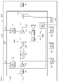
- FIG. 1 is a diagram illustrating a configuration example of a power amplifier circuit according to a first embodiment of the present disclosure.
- FIG. 2 is a diagram illustrating the spectrum of a signal inputted to an amplifier 111 of a posterior stage.
- FIG. 3 is a diagram illustrating part of the spectrum of a signal outputted from the amplifier 111 of the posterior stage.
- FIG. 4A is a graph indicating simulation results of third-order intermodulation distortion in the power amplifier circuit according to the first embodiment of the present disclosure and a comparative example.
- FIG. 4B is a graph indicating simulation results of third-order intermodulation distortion in the power amplifier circuit according to the first embodiment of the present disclosure and the comparative example.
- FIG. 5 is a diagram illustrating a configuration example of a power amplifier circuit according to a second embodiment of the present disclosure.
- FIG. 6 is a diagram illustrating a configuration example of a transmit module including the power amplifier circuit according to the first embodiment of the present disclosure.
- FIG. 7 is a diagram illustrating a configuration example of a transmit module including the power amplifier circuit according to the second embodiment of the present disclosure.
- FIG. 8 is a diagram illustrating another configuration example of a transmit module including the power amplifier circuit according to the second embodiment of the present disclosure.
- FIG. 1 is a diagram illustrating a configuration example of a power amplifier circuit according to a first embodiment of the present disclosure.
- a power amplifier circuit 100 A illustrated in FIG. 1 is provided in, for example, a mobile communication device, such as a mobile phone and used for amplifying electric power of radio frequency (RF) signals to be transmitted to base stations.
- RF radio frequency
- the power amplifier circuit 100 A amplifies power of signals of communication standards, such as the second-generation (2G) mobile communication system, the third-generation (3G) mobile communication system, the fourth-generation (4G) mobile communication, the fifth-generation (5G) mobile communication system, Long-Term Evolution Frequency-Division Duplex (LTE-FDD), Long-Term Evolution Time-Division Duplex (LTE-TDD), LTE-Advanced, and LTE-Advanced Pro.
- the frequency of RF signals ranges, for example, from about several hundreds of MHz to about several tens of GHz.
- the communication standard and the frequency of signals amplified by the power amplifier circuit 100 A are not limited to these examples.
- the power amplifier circuit 100 A includes, for example, amplifiers 110 and 111 , a power combiner 120 , matching circuits 130 and 131 , a harmonic-wave extraction circuit 140 , a distortion compensation circuit 150 A, an input terminal T 1 , and an output terminal T 2 .
- the power amplifier circuit 100 A also includes a primary path P 1 and a secondary path P 2 .
- the amplifier 110 (a third amplifier) and the amplifier 111 (a first amplifier) both amplify inputted RF signals and output the RF signals.
- the power amplifier circuit 100 A amplifies electric power in two stages.
- the amplifier 110 of a first stage (a drive stage) amplifies an RF signal RF 1 (a fourth signal) inputted from the input terminal T 1 via the matching circuit 130 and outputs an RF signal RF 2 (a third signal).
- the amplifier 111 of a posterior stage (a power stage) amplifies an RF signal RF 3 (a first signal) resulting from combination by the power combiner 120 described later and outputs an RF signal RF 4 (a second signal).
- the RF signals RF 2 and RF 4 each includes a harmonic wave including the second-harmonic wave generated by amplification of the amplifier 110 or 111 .
- the amplifiers 110 and 111 are both configured by using bipolar transistors, such as heterojunction bipolar transistors (HBTs).
- the amplifiers 110 and 111 may be configured by using field effect transistors (MOSFETs: Metal-oxide-semiconductor Field-Effect Transistors) instead of HBTs.
- the primary path P 1 is a path starting from the input terminal T 1 and leading to the output terminal T 2 via the amplifiers 110 and 111 .
- the primary path P 1 is a path along which a fundamental wave F 0 of the RF signal RF 1 travels.
- the secondary path P 2 is a path starting from the harmonic-wave extraction circuit 140 and leading to the power combiner 120 via the distortion compensation circuit 150 A, which forms a feedback circuit.
- the secondary path P 2 is a path for generating a second-harmonic wave 2F 0 to be inputted to compensate for third-order intermodulation distortion caused at the amplifier 111 of the posterior stage.
- the power combiner 120 outputs the RF signal RF 3 (the first signal) by combining the fundamental wave F 0 having traveled along the primary path P 1 and the second-harmonic wave 2F 0 having traveled along the secondary path P 2 with each other.
- the generated RF signal RF 3 is outputted to the amplifier 111 of the posterior stage.
- the matching circuit 130 (MN: Matching Network) performs impedance matching between a circuit (not illustrated in the drawing) provided in an anterior stage and the amplifier 110 .
- the matching circuit 131 is provided between the amplifier 110 and the power combiner 120 and performs impedance matching between the amplifiers 110 and 111 .
- the matching circuit 131 also has a function of attenuating harmonic distortion (HD) caused by amplification of the amplifier 110 .
- HD attenuating harmonic distortion
- the matching circuit 131 is configured as a specific example of a second-harmonic-wave attenuation circuit. This configuration hinders output of the second-harmonic wave to the power combiner 120 through the primary path P 1 .
- the matching circuit 131 may be, for example, a low-pass-filter (LPF) circuit having a frequency characteristic of passing the fundamental wave and attenuating the second-harmonic wave.
- LPF low-pass-filter
- the harmonic-wave extraction circuit 140 is provided in a subsequent stage after the amplifier 111 .
- the harmonic-wave extraction circuit 140 extracts the second-harmonic wave 2F 0 included in the RF signal RF 4 and inputs at least part of the second-harmonic wave 2F 0 to the distortion compensation circuit 150 A.
- the remainder of the signal from which the second-harmonic wave 2F 0 has been extracted by the harmonic-wave extraction circuit 140 is outputted as a transmit signal from the output terminal T 2 .
- a harmonic termination circuit that grounds a harmonic wave is used as the harmonic-wave extraction circuit 140 .
- the harmonic termination circuit may be configured to divide a second-harmonic wave inputted to the harmonic termination circuit, and then, input one part of the second-harmonic wave to the distortion compensation circuit 150 A and ground the other part of the second-harmonic wave.
- the harmonic-wave extraction circuit can be formed without necessarily increase in the circuit size.
- the harmonic-wave extraction circuit 140 is not limited to the configuration using a harmonic termination circuit, but a filter circuit or the like that extracts only the second-harmonic wave from the RF signal RF 4 may be used.
- the distortion compensation circuit 150 A is provided on the secondary path P 2 between the harmonic-wave extraction circuit 140 and the power combiner 120 .
- the distortion compensation circuit 150 A is a circuit configured to adjust the amplitude and the phase of the second-harmonic wave 2F 0 , which is deliberately added to compensate for the third-order intermodulation distortion, and outputs the second-harmonic wave 2F 0 .
- the distortion compensation circuit 150 A includes, for example, an amplitude adjustment circuit 200 , a phase adjustment circuit 210 , and a matching circuit 220 .
- the amplitude adjustment circuit 200 adjusts the amplitude of the second-harmonic wave 2F 0 extracted by the harmonic-wave extraction circuit 140 and inputs the adjusted second-harmonic wave 2F 0 to the phase adjustment circuit 210 . Since the distortion compensation circuit 150 A includes the amplitude adjustment circuit 200 , the power of the second-harmonic wave 2F 0 can be adjusted in accordance with the level of output power of the transmit signal.
- the amplitude adjustment circuit 200 may configured as, for example, an amplifier (a second amplifier) that increases the power of the second-harmonic wave. With this configuration, as the output power of the transmit signal is increased, the power of the second-harmonic wave 2F 0 can be increased. Alternatively, in the case in which the power of the second-harmonic wave 2F 0 is high relative to a power level required for distortion compensation, the amplitude adjustment circuit 200 may be configured as an attenuator.
- the phase adjustment circuit 210 is provided in, for example, a subsequent stage after the amplitude adjustment circuit 200 .
- the phase adjustment circuit 210 performs adjustment to render the phase of the inputted second-harmonic wave 2F 0 suitable for distortion compensation and outputs the second-harmonic wave 2F 0 .
- the matching circuit 220 performs impedance matching between the phase adjustment circuit 210 and the power combiner 120 .
- the distortion compensation circuit 150 A can adjust the amplitude and the phase of the second-harmonic wave 2F 0 to be deliberately inputted to the input of the amplifier 111 of the posterior stage.
- the order in which the components included in the distortion compensation circuit 150 A are arranged is not limited to this example and may be changed as appropriate.
- the amplitude adjustment circuit 200 may be provided in a subsequent stage after the phase adjustment circuit 210 .
- the power combiner 120 , the matching circuits 130 , 131 , and 220 , the harmonic-wave extraction circuit 140 , and the phase adjustment circuit 210 may be each configured to include elements, such as an inductor and a capacitor, or a resonator using acoustic waves, such as a surface-acoustic-wave (SAW) filter.
- elements such as an inductor and a capacitor, or a resonator using acoustic waves, such as a surface-acoustic-wave (SAW) filter.
- SAW surface-acoustic-wave
- FIG. 2 is a diagram illustrating the spectrum of a signal, which is the RF signal RF 3 in FIG. 1 , inputted to the amplifier 111 of the posterior stage.
- FIG. 3 is a diagram illustrating part of the spectrum of a signal, which is the RF signal RF 4 in FIG. 1 , outputted from the amplifier 111 of the posterior stage.
- the horizontal axes indicate the frequency of the signal and the vertical axes indicate the power spectral density (PSD).
- the fundamental wave F 0 having traveled along the primary path P 1 and the second-harmonic wave 2F 0 having traveled along the secondary path P 2 are inputted to the amplifier 111 of the posterior stage.
- the fundamental wave F 0 contains components of two kinds of frequencies f 1 and f 2 (f 1 ⁇ f 2 ) adjacent to each other.
- the second-harmonic wave of each of the two kinds of frequencies f 1 and f 2 is extracted by the harmonic-wave extraction circuit 140 , and thus, the second-harmonic wave 2F 0 contains components of two kinds of frequencies 2f 1 and 2f 2 .
- signals at the frequencies f 1 and f 2 and signals at the frequencies 2f 1 and 2f 2 are inputted together to the amplifier 111 .
- an amplified signal obtained by amplifying the fundamental wave F 0 is outputted as indicated in FIG. 3 .
- third-order intermodulation distortion IM 3 L with a frequency 2f 1 ⁇ f 2 occurs on a low-frequency side with respect to the fundamental wave F 0 while third-order intermodulation distortion IM 3 H with a frequency 2f 2 ⁇ f 1 occurs on a high-frequency side with respect to the fundamental wave F 0 .
- the third-order intermodulation distortions IM 3 L and IM 3 H are relatively close to the frequencies f 1 and f 2 of the fundamental wave F 0 , and hence, it is difficult to remove the third-order intermodulation distortions IM 3 L and IM 3 H by using a filter circuit or the like.
- the third-order intermodulation distortions IM 3 L and IM 3 H can be, therefore, a cause of deterioration of linearity of the amplifier.
- the amplification of the amplifier 111 also causes, for example, other kinds of distortion, such as third-order intermodulation distortions with frequencies 2f 1 +f 2 and 2f 2 +f 1 , but the frequencies of the distortions are relatively far from the frequencies f 1 and f 2 of the fundamental wave F 0 and descriptions thereof is thus omitted here.
- other kinds of distortion such as third-order intermodulation distortions with frequencies 2f 1 +f 2 and 2f 2 +f 1 , but the frequencies of the distortions are relatively far from the frequencies f 1 and f 2 of the fundamental wave F 0 and descriptions thereof is thus omitted here.
- compensation signals CS L and CS H that cancel out the third-order intermodulation distortions IM 3 L and IM 3 H are generated by deliberately adding the second-harmonic wave 2F 0 in this embodiment.
- a signal obtained by adding the fundamental wave F 0 and the second-harmonic wave 2F 0 in the power combiner 120 is inputted to the amplifier 111 , and as a result, the compensation signal CS L with a frequency (2f 1 ⁇ f 2 ), which is a difference between the frequency 2f 1 as one frequency of the second-harmonic wave 2F 0 and the frequency f 2 as the other frequency of the fundamental wave F 0 , is generated.
- a compensation signal CS H with a frequency (2f 2 ⁇ f 1 ), which is a difference between the frequency 2f 2 as the other frequency of the second-harmonic wave 2F 0 and the frequency f 1 as one frequency of the fundamental wave F 0 is generated.
- These compensation signals CS L and CS H are respectively identical in frequency to the third-order intermodulation distortions IM 3 L and IM 3 H .
- the phase adjustment circuit 210 changes the phase of the second-harmonic wave 2F 0 in such a manner that the compensation signals CS L and CS H are almost opposite in phase to the third-order intermodulation distortions IM 3 L and IM 3 H at the output of the amplifier 111 .
- the amplitude adjustment circuit 200 adjusts the amplitude of the second-harmonic wave 2F 0 in such a manner that the compensation signals CS L and CS H and the third-order intermodulation distortions IM 3 L and IM 3 H cancel each other out at the output of the amplifier 111 with respect to amplitude.
- the compensation signals CS L and CS H cancel out the third-order intermodulation distortions IM 3 L and IM 3 H .
- the compensation signals CS L and CS H are drawn in a downward direction to indicate that the compensation signals CS L and CS H are almost opposite in phase to the third-order intermodulation distortions IM 3 L and IM 3 H .
- the power amplifier circuit 100 A Due to the effect described above, in the power amplifier circuit 100 A, it is possible to reduce the effect of the third-order intermodulation distortions IM 3 L and IM 3 H occurring in the amplifier 111 . As a result, the power amplifier circuit 100 A can hinder the deterioration of linearity.
- the second-harmonic wave caused by amplification of the amplifier 111 is extracted and the second-harmonic wave is inputted to the input of the amplifier 111 by feedback.
- the present embodiment does not require newly providing a generation circuit, an amplifier, or the like to generate a second-harmonic wave.
- the power amplifier circuit 100 A can reduce the effect of intermodulation distortion without necessarily increase in the circuit size.
- a harmonic termination circuit is used as the harmonic-wave extraction circuit 140 .
- the harmonic-wave extraction circuit can be formed without necessarily increase in the circuit size.
- the distortion compensation circuit 150 A since the extracted second-harmonic wave is inputted to the distortion compensation circuit 150 A, the distortion compensation circuit 150 A does not need to include a filter circuit or the like that attenuates the fundamental wave. This configuration also can suppress increase in the circuit size. Noted that it is not intended to exclude the configuration in which a distortion compensation circuit includes a filter circuit.
- Patent Document 1 does not include a circuit between a power divider and a power combiner on a main path to attenuate the second-harmonic wave, and thus, the second-harmonic wave caused by amplification of the amplifier in the first stage passes through the primary path.
- the second-harmonic wave is generated in a secondary path
- the second-harmonic wave having traveled through the primary path and the second-harmonic wave having traveled through the secondary path may cancel each other out when the two kinds of second-harmonic waves are added together at the power combiner. Consequently, the power of the second-harmonic wave additionally inputted to the amplifier 111 may be insufficient.
- the function of attenuating the second-harmonic wave is imparted to the matching circuit 131 provided in the primary path P 1 .
- a high-power second-harmonic wave can be inputted to the amplifier 111 in comparison to the configuration disclosed in Patent Document 1. Therefore, the power amplifier circuit 100 A can increase output power and also reduce the effect of intermodulation distortion.
- the second-harmonic wave caused in the amplifier 111 of the posterior stage (the power stage) is used for additional input.
- the power amplifier circuit 100 A can increase output power and also reduce the effect of intermodulation distortion.
- the circuit provided between the amplifier 110 and the power combiner 120 and configured to attenuate a second-harmonic wave in the power amplifier circuit 100 A is not limited to the matching circuit 131 .
- an amplifier designed to amplify the frequency range of the fundamental wave F 0 may be provided instead of the matching circuit 131 . This enables attenuation of the second-harmonic wave caused by amplification of the amplifier 110 of the first stage.
- the power amplifier circuit since the power amplifier circuit includes amplifiers in three stages on the primary path P 1 , it is possible to further increase the output power of transmit signal.
- matching circuits may be provided in both anterior and posterior stages with respect to the amplifier provided instead of the matching circuit 131 .
- All the components included in the power amplifier circuit 100 A illustrated in FIG. 1 are not necessarily provided as individual circuits and one circuit may have a plurality of functions.
- the distortion compensation circuit 150 A does not include the matching circuit 220 , but instead, the phase adjustment circuit 210 has a function of the matching circuit 220 .
- FIGS. 4A and 4B are graphs indicating simulation results of third-order intermodulation distortion in the power amplifier circuit according to the first embodiment of the present disclosure and a comparative example.
- the comparative example has a configuration formed by excluding the distortion compensation circuit 150 A from the power amplifier circuit 100 A illustrated in FIG. 1 .
- FIG. 4A illustrates third-order intermodulation distortion on a low-frequency side with respect to the fundamental wave
- FIG. 4B illustrates third-order intermodulation distortion on a high-frequency side with respect to the fundamental wave.
- the horizontal axes indicate the output power Pout (dBm) of transmit signal
- the vertical axes indicate the output level (dBc) of third-order intermodulation distortion with respect to the fundamental wave.
- the output level of third-order intermodulation distortion steeply rises after the output level exceeds a particular output power level.
- the output power of the comparative example is approximately 28 dBm while the output power of the present embodiment is approximately 29 dBm, which indicates that the output power of the present embodiment is improved by approximately 1.0 dB as compared to the comparative example.
- FIG. 4A the output power of the comparative example is approximately 28 dBm while the output power of the present embodiment is approximately 29 dBm, which indicates that the output power of the present embodiment is improved by approximately 1.0 dB as compared to the comparative example.
- the output power of the comparative example is approximately 27.5 dBm while the output power of the present embodiment is approximately 29 dBm, which indicates that the output power of the present embodiment is improved by approximately 1.5 dB as compared to the comparative example. According to these results, it is understood that the present embodiment increases output power and also reduces the effect of intermodulation distortion.
- FIG. 5 is a diagram illustrating a configuration example of a power amplifier circuit according to the second embodiment of the present disclosure.
- descriptions about specifics common to those of the first embodiment are not repeated and only different points are explained.
- almost identical effects and advantages achieved by almost identical configurations are not mentioned in every embodiment.
- a power amplifier circuit 100 B illustrated in FIG. 5 includes a distortion compensation circuit 150 B instead of the distortion compensation circuit 150 A as compared to the power amplifier circuit 100 A illustrated in FIG. 1 .
- the distortion compensation circuit 150 B further includes a filter circuit 230 as compared to the distortion compensation circuit 150 A.
- the filter circuit 230 is provided between the harmonic-wave extraction circuit 140 and the power combiner 120 (in the present embodiment, between the harmonic-wave extraction circuit 140 and the amplitude adjustment circuit 200 ).
- the filter circuit 230 is provided for the case in which attenuation of the signal excluding the second-harmonic wave is insufficient when the harmonic-wave extraction circuit 140 extracts the second-harmonic wave, so that the filter circuit 230 is configured to attenuate the signal of a frequency different from the frequency of the second-harmonic wave.
- the configuration of the filter circuit 230 is not limited to any specific example, but the filter circuit 230 may be configured to include, for example, an inductor and a capacitor, or a resonator using acoustic waves, such as a SAW filter.
- the power amplifier circuit 100 B can improve the reliability of reduction of third-order intermodulation distortion as compared to the power amplifier circuit 100 A.
- the position of the filter circuit 230 in the distortion compensation circuit 150 B is not limited to the example described above and may be changed as appropriate.
- the filter circuit 230 can be positioned in an anterior stage with respect to the amplitude adjustment circuit 200 because the power of the inputted signal is small in comparison to the configuration in which the filter circuit 230 is positioned in a posterior stage with respect to the amplitude adjustment circuit 200 .
- FIG. 6 is a diagram illustrating a configuration example of a transmit module including the power amplifier circuit according to the first embodiment of the present disclosure.
- a transmit module 300 A includes a semiconductor chip 20 A, a matching circuit 132 , and bias networks 180 to 182 , which are provided at a module substrate 10 A.
- the power amplifier circuit 100 A according to the first embodiment and bias circuits 170 to 172 are provided in an integrated manner.
- the matching circuit 132 performs impedance matching between the power amplifier circuit 100 A provided in an anterior stage and another circuit (not illustrated in the drawing) provided in a posterior stage after the power amplifier circuit 100 A.
- the matching circuit 132 may be formed inside the semiconductor chip 20 A.
- the bias networks 180 to 182 supply a power supply voltage respectively to the amplifiers 110 and 111 , and the amplitude adjustment circuit 200 .
- a battery voltage Vbatt is supplied to the bias circuits 170 to 172 and the bias circuits 170 to 172 in turn supply a bias current or a bias voltage respectively to the amplifiers 110 and 111 and the amplitude adjustment circuit 200 in accordance with control signals Ctrl 1 to Ctrl 3 inputted from outside of the module substrate 10 A.
- the power amplifier circuit 100 A including the distortion compensation circuit 150 A and the bias circuits 170 to 172 are provided at the same semiconductor chip 20 A in an integrated manner, it is possible to downsize the transmit module in comparison to, for example, a configuration in which the distortion compensation circuit 150 A is formed outside the semiconductor chip 20 A.
- FIG. 7 is a diagram illustrating a configuration example of a transmit module including the power amplifier circuit according to the second embodiment of the present disclosure.
- a transmit module 300 B differs from the transmit module 300 A in that a semiconductor chip 20 B instead of the semiconductor chip 20 A is provided at a module substrate 10 B.
- the semiconductor chip 20 B includes the power amplifier circuit 100 B according to the second embodiment.
- the power amplifier circuit 100 B including the distortion compensation circuit 150 B and the bias circuits 170 to 172 are provided at the same semiconductor chip 20 B in an integrated manner, it is possible to downsize the transmit module.
- FIG. 8 is a diagram illustrating another configuration example of a transmit module including the power amplifier circuit according to the second embodiment of the present disclosure.
- a transmit module 300 C differs from the transmit module 300 A in that the filter circuit 230 included in the distortion compensation circuit 150 B is formed outside a semiconductor chip 20 C. This means that, in this configuration example, a harmonic wave outputted from the harmonic-wave extraction circuit 140 once moves out of the semiconductor chip 20 C and returns again to the semiconductor chip 20 C through the filter circuit 230 .
- the filter circuit 230 is configured as, for example, a SAW filter, it is possible to reduce the cost in comparison to a configuration in which the filter circuit 230 is formed at the semiconductor chip 20 C.
- the filter circuit 230 may be provided at, for example, a module substrate 10 C by using a surface mount device (SMD).
- SMD surface mount device
- the transmit modules 300 A to 300 C described above may each constitute a high-frequency module in conjunction with a receive module including a low-noise amplifier (LNA). Furthermore, a plurality of any kind of the transmit modules 300 A to 300 C may constitute a multiband high-frequency module in conjunction with a plurality of receive modules. In this case, the plurality of modules respond respectively to signals at different frequency bands.
- the multiband high-frequency module may include modules respectively supporting a frequency division duplex (FDD) technique and a time division duplex (TDD) technique.
- the power amplifier circuits 100 A and 100 B includes the amplifier 111 configured to amplify the RF signal RF 3 and output the RF signal RF 4 , the harmonic-wave extraction circuit 140 configured to extract a second-harmonic wave included in the RF signal RF 4 , the phase adjustment circuit 210 configured to adjust the phase of the extracted second-harmonic wave, and the power combiner 120 configured to combine the second-harmonic wave of the adjusted phase with the RF signal RF 2 and output the RF signal RF 3 .
- the power amplifier circuits 100 A and 100 B do not need to additionally include a generation circuit, an amplifier, or the like to generate a second-harmonic wave.
- the power amplifier circuits 100 A and 100 B can reduce the effect of the intermodulation distortions IM 3 L and IM 3 H without necessarily increase in the circuit size.
- the phase adjustment circuit 210 changes the phase of the second-harmonic wave 2F 0 in such a manner that the signals obtained as the differences between the second-harmonic wave 2F 0 and the fundamental wave F 0 included in the RF signal RF 3 and the third-order intermodulation distortions IM 3 L and IM 3 H occurring in the amplifier 111 are substantially in antiphase at the output of the amplifier 111 .
- the compensation signals CS L and CS H cancel out the third-order intermodulation distortions IM 3 L and IM 3 H , and as a result, it is possible to reduce the effect of intermodulation distortion.
- the power amplifier circuits 100 A and 100 B further include the amplitude adjustment circuit 200 configured to adjust the amplitude of the second-harmonic wave 2F 0 in such a manner that the signals obtained as the differences between the second-harmonic wave 2F 0 and the fundamental wave F 0 included in the RF signal RF 3 and the third-order intermodulation distortions IM 3 L and IM 3 H occurring in the amplifier 111 cancel each other out at the output of the amplifier 111 .
- the power of the second-harmonic wave 2F 0 can be adjusted in accordance with the level of output power of the transmit signal.
- the amplitude adjustment circuit 200 may be configured as an amplifier that amplifies the power of the second-harmonic wave 2F 0 . With this configuration, as the output power of the transmit signal is increased, the power of the second-harmonic wave 2F 0 can be increased.
- the power amplifier circuits 100 A and 100 B further include the amplifier 110 configured to amplify the RF signal RF 1 and output the RF signal RF 2 and the matching circuit 131 provided between the amplifier 110 and the power combiner 120 and configured to attenuate a signal at the frequency of the second-harmonic wave 2F 0 .
- This configuration avoids the second-harmonic wave having traveled along the primary path P 1 and the second-harmonic wave having traveled along the secondary path P 2 cancelling each other out at the power combiner 120 .
- a high-power second-harmonic wave can be inputted to the amplifier 111 in comparison to the configuration disclosed in Patent Document 1.
- the power amplifier circuit 100 B further includes the filter circuit 230 provided between the harmonic-wave extraction circuit 140 and the power combiner 120 and configured to attenuate a signal at a frequency different from the frequency of the second-harmonic wave.
- the filter circuit 230 is formed outside the semiconductor chip 20 C at which the amplifier 111 is formed. In the case in which the filter circuit 230 is configured as, for example, a SAW filter, it is possible to reduce the cost in comparison to a configuration in which the filter circuit 230 is formed at the semiconductor chip 20 C.
Landscapes
- Engineering & Computer Science (AREA)
- Power Engineering (AREA)
- Physics & Mathematics (AREA)
- Nonlinear Science (AREA)
- Microelectronics & Electronic Packaging (AREA)
- Amplifiers (AREA)
Applications Claiming Priority (4)
| Application Number | Priority Date | Filing Date | Title |
|---|---|---|---|
| JP2018-008868 | 2018-01-23 | ||
| JP2018008868 | 2018-01-23 | ||
| JPJP2018-008868 | 2018-01-23 | ||
| PCT/JP2019/001688 WO2019146550A1 (ja) | 2018-01-23 | 2019-01-21 | 電力増幅回路 |
Related Parent Applications (1)
| Application Number | Title | Priority Date | Filing Date |
|---|---|---|---|
| PCT/JP2019/001688 Continuation WO2019146550A1 (ja) | 2018-01-23 | 2019-01-21 | 電力増幅回路 |
Publications (2)
| Publication Number | Publication Date |
|---|---|
| US20200343863A1 US20200343863A1 (en) | 2020-10-29 |
| US11418151B2 true US11418151B2 (en) | 2022-08-16 |
Family
ID=67395354
Family Applications (1)
| Application Number | Title | Priority Date | Filing Date |
|---|---|---|---|
| US16/928,084 Active US11418151B2 (en) | 2018-01-23 | 2020-07-14 | Power amplifier circuit |
Country Status (3)
| Country | Link |
|---|---|
| US (1) | US11418151B2 (ja) |
| CN (1) | CN111615787B (ja) |
| WO (1) | WO2019146550A1 (ja) |
Citations (13)
| Publication number | Priority date | Publication date | Assignee | Title |
|---|---|---|---|---|
| JPS5573115A (en) * | 1978-11-27 | 1980-06-02 | Nec Corp | Traveling wave tube amplifying device |
| JPH05243860A (ja) | 1992-02-28 | 1993-09-21 | Fujitsu Ltd | 増幅回路 |
| JP2000232325A (ja) | 1999-02-08 | 2000-08-22 | Japan Radio Co Ltd | 増幅回路における歪補償方法 |
| JP2001217659A (ja) | 2000-02-03 | 2001-08-10 | Mitsubishi Electric Corp | マイクロ波増幅器 |
| US20010048346A1 (en) | 2000-05-30 | 2001-12-06 | Toru Matsuura | Predistortion circuit, low-distortion power amplifier, and control methods therefor |
| JP2002057533A (ja) | 2000-05-30 | 2002-02-22 | Matsushita Electric Ind Co Ltd | 前置歪み補償回路、低歪み電力増幅器、及びその制御方法 |
| JP2002064340A (ja) | 2000-08-14 | 2002-02-28 | Matsushita Electric Ind Co Ltd | 高周波電力増幅器 |
| US20030071684A1 (en) * | 1999-12-17 | 2003-04-17 | Basim Noori | Linearisation method and signal processing device |
| US20050242877A1 (en) | 2004-04-30 | 2005-11-03 | Sony Ericsson Mobile Communications Japan, Inc. | Distortion compensating and power amplifying apparatus |
| US20080058001A1 (en) | 2006-09-01 | 2008-03-06 | Sony Ericsson Mobile Communications Japan, Inc. | Power amplifier system and mobile phone terminal using same |
| JP2008219453A (ja) | 2007-03-05 | 2008-09-18 | Alps Electric Co Ltd | 送受信回路モジュール |
| US20120099624A1 (en) * | 2010-10-26 | 2012-04-26 | Fujitsu Limited | Communication device and method of reducing harmonics transmitted |
| US20170338775A1 (en) | 2016-05-19 | 2017-11-23 | Murata Manufacturing Co., Ltd. | Power amplifier module |
Family Cites Families (1)
| Publication number | Priority date | Publication date | Assignee | Title |
|---|---|---|---|---|
| CN106685467B (zh) * | 2017-01-04 | 2019-02-15 | 电子科技大学 | 一种二倍频程宽带高效功率放大器 |
-
2019
- 2019-01-21 CN CN201980008561.7A patent/CN111615787B/zh active Active
- 2019-01-21 WO PCT/JP2019/001688 patent/WO2019146550A1/ja active Application Filing
-
2020
- 2020-07-14 US US16/928,084 patent/US11418151B2/en active Active
Patent Citations (15)
| Publication number | Priority date | Publication date | Assignee | Title |
|---|---|---|---|---|
| JPS5573115A (en) * | 1978-11-27 | 1980-06-02 | Nec Corp | Traveling wave tube amplifying device |
| JPH05243860A (ja) | 1992-02-28 | 1993-09-21 | Fujitsu Ltd | 増幅回路 |
| JP2000232325A (ja) | 1999-02-08 | 2000-08-22 | Japan Radio Co Ltd | 増幅回路における歪補償方法 |
| US20030071684A1 (en) * | 1999-12-17 | 2003-04-17 | Basim Noori | Linearisation method and signal processing device |
| JP2001217659A (ja) | 2000-02-03 | 2001-08-10 | Mitsubishi Electric Corp | マイクロ波増幅器 |
| US20010048346A1 (en) | 2000-05-30 | 2001-12-06 | Toru Matsuura | Predistortion circuit, low-distortion power amplifier, and control methods therefor |
| JP2002057533A (ja) | 2000-05-30 | 2002-02-22 | Matsushita Electric Ind Co Ltd | 前置歪み補償回路、低歪み電力増幅器、及びその制御方法 |
| JP2002064340A (ja) | 2000-08-14 | 2002-02-28 | Matsushita Electric Ind Co Ltd | 高周波電力増幅器 |
| US20050242877A1 (en) | 2004-04-30 | 2005-11-03 | Sony Ericsson Mobile Communications Japan, Inc. | Distortion compensating and power amplifying apparatus |
| US20080058001A1 (en) | 2006-09-01 | 2008-03-06 | Sony Ericsson Mobile Communications Japan, Inc. | Power amplifier system and mobile phone terminal using same |
| JP2008061123A (ja) | 2006-09-01 | 2008-03-13 | Sony Ericsson Mobilecommunications Japan Inc | 電力増幅装置および携帯電話端末 |
| JP2008219453A (ja) | 2007-03-05 | 2008-09-18 | Alps Electric Co Ltd | 送受信回路モジュール |
| US20120099624A1 (en) * | 2010-10-26 | 2012-04-26 | Fujitsu Limited | Communication device and method of reducing harmonics transmitted |
| US20170338775A1 (en) | 2016-05-19 | 2017-11-23 | Murata Manufacturing Co., Ltd. | Power amplifier module |
| JP2017208729A (ja) | 2016-05-19 | 2017-11-24 | 株式会社村田製作所 | 電力増幅モジュール |
Non-Patent Citations (7)
| Title |
|---|
| International Search Report issued in Application No. PCT/JP2019/001688, dated Mar. 26, 2019. |
| Jeon et al. "An analog linearizer using second harmonic signal mixing operation" Microwave Conference Proceedings, 2005. APMC 2005 (Year: 2005). * |
| Jeon et al., "An Analog Linearizer Based on Amplitude Modulation with Even Harmonic Signals", Microwave Journal, Feb. 2009 (Year: 2009). * |
| Kaho et al., "A Distortion Control Technique for Achieving High Power Efficiency in an HPA Array", IEEE Transactions on Microwave Theory and Techniques, vol. 50, No. 11, Nov. 2002, pp. 2505-2512. (Year: 2002). * |
| Singh et al., "Second- and Third-order Signal Predistortion for Nonlinear Distortion Suppression in a Traveling Wave Tube", IEEE Transactions on Electron Devices 52(5):709-717, Jun. 2005 (Year: 2005). * |
| Written Opinion issued in Application No. PCT/JP2019/001688, dated Mar. 26, 2019. |
| Yong et al. "A Design of Predistortion Linearizer Using Second Harmonic Signals", The Journal of Korean Institute of Electromagnetic Engineering and Science, 16(12), 2005 (Year: 2005). * |
Also Published As
| Publication number | Publication date |
|---|---|
| CN111615787B (zh) | 2023-08-11 |
| WO2019146550A1 (ja) | 2019-08-01 |
| CN111615787A (zh) | 2020-09-01 |
| US20200343863A1 (en) | 2020-10-29 |
Similar Documents
| Publication | Publication Date | Title |
|---|---|---|
| US10348248B2 (en) | Power amplifier module | |
| US20190028062A1 (en) | Load modulation amplifier | |
| US9705451B2 (en) | Power amplification module | |
| US10483928B2 (en) | Power amplification module | |
| KR20060047541A (ko) | 일그러짐 보상 전력 증폭 장치 | |
| US9369095B2 (en) | Unbalanced linear power amplifier | |
| KR20180073433A (ko) | 통신 모듈 | |
| US11750152B2 (en) | Power amplifier circuit | |
| US10439560B2 (en) | Power amplification module | |
| KR102611706B1 (ko) | 전력 증폭 회로 | |
| US11418151B2 (en) | Power amplifier circuit | |
| US20220311388A1 (en) | Power amplifier circuit, radio-frequency circuit, and communication device | |
| CN210327513U (zh) | 功率放大电路 | |
| CN113572439B (zh) | 功率放大电路 | |
| JP2019118094A (ja) | 電力増幅回路 | |
| CN111064438A (zh) | 模拟预失真电路、功率放大器及射频模块 |
Legal Events
| Date | Code | Title | Description |
|---|---|---|---|
| AS | Assignment |
Owner name: MURATA MANUFACTURING CO., LTD., JAPAN Free format text: ASSIGNMENT OF ASSIGNORS INTEREST;ASSIGNOR:HASE, MASATOSHI;REEL/FRAME:053200/0191 Effective date: 20200703 |
|
| FEPP | Fee payment procedure |
Free format text: ENTITY STATUS SET TO UNDISCOUNTED (ORIGINAL EVENT CODE: BIG.); ENTITY STATUS OF PATENT OWNER: LARGE ENTITY |
|
| STPP | Information on status: patent application and granting procedure in general |
Free format text: DOCKETED NEW CASE - READY FOR EXAMINATION |
|
| STPP | Information on status: patent application and granting procedure in general |
Free format text: NON FINAL ACTION MAILED |
|
| STPP | Information on status: patent application and granting procedure in general |
Free format text: EX PARTE QUAYLE ACTION MAILED |
|
| STPP | Information on status: patent application and granting procedure in general |
Free format text: NOTICE OF ALLOWANCE MAILED -- APPLICATION RECEIVED IN OFFICE OF PUBLICATIONS |
|
| STPP | Information on status: patent application and granting procedure in general |
Free format text: PUBLICATIONS -- ISSUE FEE PAYMENT VERIFIED |
|
| STCF | Information on status: patent grant |
Free format text: PATENTED CASE |