US11260646B2 - Methods for processing a substrate - Google Patents
Methods for processing a substrate Download PDFInfo
- Publication number
- US11260646B2 US11260646B2 US16/349,845 US201716349845A US11260646B2 US 11260646 B2 US11260646 B2 US 11260646B2 US 201716349845 A US201716349845 A US 201716349845A US 11260646 B2 US11260646 B2 US 11260646B2
- Authority
- US
- United States
- Prior art keywords
- carrier
- substrate
- debond
- location
- lifting
- Prior art date
- Legal status (The legal status is an assumption and is not a legal conclusion. Google has not performed a legal analysis and makes no representation as to the accuracy of the status listed.)
- Active
Links
Images


Classifications
-
- B—PERFORMING OPERATIONS; TRANSPORTING
- B32—LAYERED PRODUCTS
- B32B—LAYERED PRODUCTS, i.e. PRODUCTS BUILT-UP OF STRATA OF FLAT OR NON-FLAT, e.g. CELLULAR OR HONEYCOMB, FORM
- B32B43/00—Operations specially adapted for layered products and not otherwise provided for, e.g. repairing; Apparatus therefor
- B32B43/006—Delaminating
-
- H—ELECTRICITY
- H10—SEMICONDUCTOR DEVICES; ELECTRIC SOLID-STATE DEVICES NOT OTHERWISE PROVIDED FOR
- H10P—GENERIC PROCESSES OR APPARATUS FOR THE MANUFACTURE OR TREATMENT OF DEVICES COVERED BY CLASS H10
- H10P72/00—Handling or holding of wafers, substrates or devices during manufacture or treatment thereof
- H10P72/04—Apparatus for manufacture or treatment
- H10P72/0428—Apparatus for mechanical treatment or grinding or cutting
-
- H—ELECTRICITY
- H10—SEMICONDUCTOR DEVICES; ELECTRIC SOLID-STATE DEVICES NOT OTHERWISE PROVIDED FOR
- H10P—GENERIC PROCESSES OR APPARATUS FOR THE MANUFACTURE OR TREATMENT OF DEVICES COVERED BY CLASS H10
- H10P72/00—Handling or holding of wafers, substrates or devices during manufacture or treatment thereof
- H10P72/70—Handling or holding of wafers, substrates or devices during manufacture or treatment thereof for supporting or gripping
- H10P72/78—Handling or holding of wafers, substrates or devices during manufacture or treatment thereof for supporting or gripping using vacuum or suction, e.g. Bernoulli chucks
-
- B—PERFORMING OPERATIONS; TRANSPORTING
- B32—LAYERED PRODUCTS
- B32B—LAYERED PRODUCTS, i.e. PRODUCTS BUILT-UP OF STRATA OF FLAT OR NON-FLAT, e.g. CELLULAR OR HONEYCOMB, FORM
- B32B2457/00—Electrical equipment
- B32B2457/20—Displays, e.g. liquid crystal displays, plasma displays
-
- B—PERFORMING OPERATIONS; TRANSPORTING
- B32—LAYERED PRODUCTS
- B32B—LAYERED PRODUCTS, i.e. PRODUCTS BUILT-UP OF STRATA OF FLAT OR NON-FLAT, e.g. CELLULAR OR HONEYCOMB, FORM
- B32B38/00—Ancillary operations in connection with laminating processes
- B32B38/10—Removing layers, or parts of layers, mechanically or chemically
- B32B38/105—Removing layers, or parts of layers, mechanically or chemically on edges
-
- B—PERFORMING OPERATIONS; TRANSPORTING
- B32—LAYERED PRODUCTS
- B32B—LAYERED PRODUCTS, i.e. PRODUCTS BUILT-UP OF STRATA OF FLAT OR NON-FLAT, e.g. CELLULAR OR HONEYCOMB, FORM
- B32B38/00—Ancillary operations in connection with laminating processes
- B32B38/18—Handling of layers or the laminate
- B32B38/1858—Handling of layers or the laminate using vacuum
-
- H01L2221/68304—
-
- H01L2221/68386—
-
- H—ELECTRICITY
- H10—SEMICONDUCTOR DEVICES; ELECTRIC SOLID-STATE DEVICES NOT OTHERWISE PROVIDED FOR
- H10P—GENERIC PROCESSES OR APPARATUS FOR THE MANUFACTURE OR TREATMENT OF DEVICES COVERED BY CLASS H10
- H10P72/00—Handling or holding of wafers, substrates or devices during manufacture or treatment thereof
- H10P72/70—Handling or holding of wafers, substrates or devices during manufacture or treatment thereof for supporting or gripping
- H10P72/74—Handling or holding of wafers, substrates or devices during manufacture or treatment thereof for supporting or gripping using temporarily an auxiliary support
- H10P72/744—Details of chemical or physical process used for separating the auxiliary support from a device or a wafer
- H10P72/7442—Separation by peeling
-
- Y—GENERAL TAGGING OF NEW TECHNOLOGICAL DEVELOPMENTS; GENERAL TAGGING OF CROSS-SECTIONAL TECHNOLOGIES SPANNING OVER SEVERAL SECTIONS OF THE IPC; TECHNICAL SUBJECTS COVERED BY FORMER USPC CROSS-REFERENCE ART COLLECTIONS [XRACs] AND DIGESTS
- Y10—TECHNICAL SUBJECTS COVERED BY FORMER USPC
- Y10S—TECHNICAL SUBJECTS COVERED BY FORMER USPC CROSS-REFERENCE ART COLLECTIONS [XRACs] AND DIGESTS
- Y10S156/00—Adhesive bonding and miscellaneous chemical manufacture
- Y10S156/918—Delaminating processes adapted for specified product, e.g. delaminating medical specimen slide
- Y10S156/93—Semiconductive product delaminating, e.g. delaminating emiconductive wafer from underlayer
-
- Y—GENERAL TAGGING OF NEW TECHNOLOGICAL DEVELOPMENTS; GENERAL TAGGING OF CROSS-SECTIONAL TECHNOLOGIES SPANNING OVER SEVERAL SECTIONS OF THE IPC; TECHNICAL SUBJECTS COVERED BY FORMER USPC CROSS-REFERENCE ART COLLECTIONS [XRACs] AND DIGESTS
- Y10—TECHNICAL SUBJECTS COVERED BY FORMER USPC
- Y10S—TECHNICAL SUBJECTS COVERED BY FORMER USPC CROSS-REFERENCE ART COLLECTIONS [XRACs] AND DIGESTS
- Y10S156/00—Adhesive bonding and miscellaneous chemical manufacture
- Y10S156/934—Apparatus having delaminating means adapted for delaminating a specified article
- Y10S156/941—Means for delaminating semiconductive product
-
- Y—GENERAL TAGGING OF NEW TECHNOLOGICAL DEVELOPMENTS; GENERAL TAGGING OF CROSS-SECTIONAL TECHNOLOGIES SPANNING OVER SEVERAL SECTIONS OF THE IPC; TECHNICAL SUBJECTS COVERED BY FORMER USPC CROSS-REFERENCE ART COLLECTIONS [XRACs] AND DIGESTS
- Y10—TECHNICAL SUBJECTS COVERED BY FORMER USPC
- Y10T—TECHNICAL SUBJECTS COVERED BY FORMER US CLASSIFICATION
- Y10T156/00—Adhesive bonding and miscellaneous chemical manufacture
- Y10T156/11—Methods of delaminating, per se; i.e., separating at bonding face
- Y10T156/1126—Using direct fluid current against work during delaminating
- Y10T156/1132—Using vacuum directly against work during delaminating
-
- Y—GENERAL TAGGING OF NEW TECHNOLOGICAL DEVELOPMENTS; GENERAL TAGGING OF CROSS-SECTIONAL TECHNOLOGIES SPANNING OVER SEVERAL SECTIONS OF THE IPC; TECHNICAL SUBJECTS COVERED BY FORMER USPC CROSS-REFERENCE ART COLLECTIONS [XRACs] AND DIGESTS
- Y10—TECHNICAL SUBJECTS COVERED BY FORMER USPC
- Y10T—TECHNICAL SUBJECTS COVERED BY FORMER US CLASSIFICATION
- Y10T156/00—Adhesive bonding and miscellaneous chemical manufacture
- Y10T156/11—Methods of delaminating, per se; i.e., separating at bonding face
- Y10T156/1168—Gripping and pulling work apart during delaminating
-
- Y—GENERAL TAGGING OF NEW TECHNOLOGICAL DEVELOPMENTS; GENERAL TAGGING OF CROSS-SECTIONAL TECHNOLOGIES SPANNING OVER SEVERAL SECTIONS OF THE IPC; TECHNICAL SUBJECTS COVERED BY FORMER USPC CROSS-REFERENCE ART COLLECTIONS [XRACs] AND DIGESTS
- Y10—TECHNICAL SUBJECTS COVERED BY FORMER USPC
- Y10T—TECHNICAL SUBJECTS COVERED BY FORMER US CLASSIFICATION
- Y10T156/00—Adhesive bonding and miscellaneous chemical manufacture
- Y10T156/19—Delaminating means
- Y10T156/1928—Differential fluid pressure delaminating means
- Y10T156/1944—Vacuum delaminating means [e.g., vacuum chamber, etc.]
-
- Y—GENERAL TAGGING OF NEW TECHNOLOGICAL DEVELOPMENTS; GENERAL TAGGING OF CROSS-SECTIONAL TECHNOLOGIES SPANNING OVER SEVERAL SECTIONS OF THE IPC; TECHNICAL SUBJECTS COVERED BY FORMER USPC CROSS-REFERENCE ART COLLECTIONS [XRACs] AND DIGESTS
- Y10—TECHNICAL SUBJECTS COVERED BY FORMER USPC
- Y10T—TECHNICAL SUBJECTS COVERED BY FORMER US CLASSIFICATION
- Y10T156/00—Adhesive bonding and miscellaneous chemical manufacture
- Y10T156/19—Delaminating means
- Y10T156/1978—Delaminating bending means
- Y10T156/1989—Corner edge bending delaminating means
Definitions
- the present disclosure relates generally to methods of processing a substrate and, more particularly, to methods of processing a substrate by initiating debonding at a location of an outer peripheral bonded interface between the substrate and a carrier.
- Glass sheets are commonly used, for example, in display applications, for example liquid crystal displays (LCDs), electrophoretic displays (EPD), organic light emitting diode displays (OLEDs), plasma display panels (PDPs), touch sensors, photovoltaics, or the like.
- LCDs liquid crystal displays
- EPD electrophoretic displays
- OLEDs organic light emitting diode displays
- PDPs plasma display panels
- touch sensors photovoltaics, or the like.
- Glass sheets are commonly fabricated by flowing molten glass to a forming body whereby a glass ribbon may be formed by a variety of ribbon forming processes, for example, slot draw, float, down-draw, fusion down-draw, rolling, or up-draw.
- the glass ribbon may then be subsequently divided to provide thin, flexible sheets of glass suitable for further processing into a desired display application including, but not limited to, a substrate for mobile devices, wearables (e.g., watches), televisions, computers, tablets, and other display monitors.
- a substrate for mobile devices wearables (e.g., watches), televisions, computers, tablets, and other display monitors.
- the flexible glass is bonded to a carrier.
- the characteristics and size of the carrier allow the bonded structure to be handled and transported in production without undesired bending of the glass sheet and without causing damage to the glass sheet.
- a thin, flexible glass sheets may be bonded to a relatively rigid carrier, and then functional components (e.g., a color filter, touch sensor, or thin-film transistor (TFT) components) may be attached to the thin, flexible glass sheet to produce a glass substrate that may be used in the production of electronic devices for display applications.
- TFT thin-film transistor
- Methods of processing the substrate may, for example, include initiation of debonding between the substrate and the one or more carriers as well as complete separation of the substrate and the one or more carriers.
- Single substrates throughout the disclosure include a wide range of substrates including a single glass substrate (e.g., a single flexible glass substrate, or single rigid glass substrate), a single glass-ceramic substrate, a single ceramic substrate, or a single silicon substrate.
- glass is meant to include any material made at least partially of glass, including glass and glass-ceramics.
- Glass-ceramics include materials produced through controlled crystallization of glass. In embodiments, glass-ceramics have about 30% to about 90% crystallinity.
- Non-limiting examples of glass ceramic systems that may be used include Li 2 O ⁇ Al 2 O 3 ⁇ nSiO 2 (i.e.
- the single substrate includes a single blank substrate of material, for example a single blank glass substrate (e.g., a glass sheet including pristine surfaces separated from a glass ribbon produced by a down-draw fusion process or other technique), a single blank glass-ceramic substrate, a single blank silicon substrate (e.g., a single blank silicon wafer).
- a single blank glass substrate e.g., a glass sheet including pristine surfaces separated from a glass ribbon produced by a down-draw fusion process or other technique
- a single blank glass-ceramic substrate e.g., a single blank silicon wafer.
- the single blank glass substrate may be transparent, translucent, or opaque and may optionally include the same glass composition throughout the entire thickness of the single blank glass substrate from a first major surface to a second major surface of the single blank glass substrate.
- the single blank glass substrate may include a single blank glass substrate that has been chemically strengthened.
- single glass substrates may include features that allow the single substrate to modify light or be incorporated into a display device, touch sensor component, or other device.
- the single glass substrate may include color filters, polarizers, thin-film transistors (TFT) or other components.
- TFT thin-film transistors
- the single silicon substrate may include features that allow the single silicon substrate to be incorporated into an integrated circuit, a photovoltaic device, or other electrical component.
- the substrate may include a stack of single substrates, including, for example, any one or more single substrates.
- the stack of single substrates may be built by two or more single substrates stacked relative to one another with facing major surfaces of adjacent single substrates being bonded relative to one another.
- the stack of single substrates may include a stack of single glass substrates.
- a first single glass substrate may include a color filter and a second single glass substrate may include one or more thin-film transistors.
- the first and second single glass substrates may be bonded together as a stack of single substrates that may be formed as a display panel for display applications.
- substrates of the present disclosure may include any one or more single substrates or stack of single substrates.
- a substrate e.g., one or more single substrates, stack of single substrates
- a first major surface of the substrate may be bonded to a single carrier.
- both major surfaces of a substrate may be bonded to respective carriers with the substrate positioned between the respective carriers.
- the present disclosure provides exemplary embodiments of the substrate and the one or more carriers that facilitate initiation of debonding and complete separation of the carriers from the substrate.
- the substrate and the one or more carriers that facilitate initiation of debonding and complete separation of the carriers from the substrate.
- the initial location of the bonded interface, where debonding is initiated provides a desired point of weakness in the bonded interface.
- subsequent peeling techniques may involve significantly less force as debonding has already been initiated. Because there is a reduction in the maximum applied force to completely separate the carrier from the substrate (e.g., by way of peeling), the associated stress applied to the substrate is likewise reduced, thereby further reducing possible damage to the substrate.
- a method of processing a substrate with a first major surface of the substrate removably bonded to a first major surface of a first carrier and a second major surface of the substrate removably bonded to a first major surface of a second carrier includes initiating debonding at a first location of an outer peripheral bonded interface between the substrate and the first carrier to separate a portion of the first carrier from the substrate.
- the method further includes propagating a first debond front from the first debonded location along a first direction extending away from the first debonded location by sequentially applying a plurality of lifting forces to the first carrier at a corresponding plurality of sequential lifting locations of the first carrier. Each lifting force of the plurality of lifting forces is sequentially applied at a corresponding lifting location of the plurality of sequential lifting locations after the first debond front has propagated past the corresponding lifting location of the first carrier.
- the method of embodiment 1, includes sequentially applying the plurality of lifting forces to the first carrier at the corresponding plurality of sequential lifting locations of the first carrier to propagate the first debond front until the first carrier is completely separated from the substrate.
- the plurality of lifting forces are sequentially applied by a corresponding plurality of suction cups arranged along the first direction.
- the plurality of suction cups engage the first carrier prior to propagating the first debond front the plurality of lifting forces are sequentially applied by a respective suction cup of the plurality of suction cups after the first debond front propagates past the respective suction cup and before the first debond front propagates past an immediately adjacent suction cup of the plurality of suctions cups arranged downstream from the respective suction cup along the first direction.
- the method of any one of embodiments 1-4 includes continuously propagating the first debond front without ceasing propagation of the first debond front until the first carrier is completely separated from the substrate.
- the method of any one of embodiments 1-5 includes decreasing bond energy between the substrate and the first carrier based on thermoelectric effect.
- decreasing bond energy between the substrate and the first carrier includes decreasing a temperature of the first carrier.
- the method of any one of embodiments 1-7 includes inhibiting bending of the second carrier while applying the plurality of lifting forces to the first carrier.
- inhibiting bending of the second carrier includes removably attaching a second major surface of the second carrier to a plate to inhibit bending of the second carrier while applying the plurality of lifting forces to the first carrier.
- the first location of the outer peripheral bonded interface between the substrate and the first carrier includes a corner portion of the substrate defined between an intersection of a first edge and a second edge of the substrate.
- the first direction extends from the corner portion of the substrate diagonally across the substrate.
- the first location of the outer peripheral bonded interface between the substrate and the first carrier includes an outer peripheral edge of the substrate, the first direction extends perpendicular to the outer peripheral edge of the substrate and across the substrate.
- the method of embodiment 2 includes, after completely separating the first carrier from the substrate, then initiating debonding at a second location of an outer peripheral bonded interface between the substrate and the second carrier to separate a portion of the second carrier from the substrate.
- the method further includes propagating a second debond front from the debonded location along a second direction extending away from the second debonded location by sequentially applying a plurality of lifting forces to the second carrier at a corresponding plurality of sequential lifting locations of the second carrier. Each lifting force of the plurality of lifting forces is sequentially applied to a corresponding lifting location of the plurality of sequential lifting locations after the second debond front has propagated past the corresponding lifting location of the second carrier.
- the method of embodiment 13 includes sequentially applying the plurality of lifting forces to the second carrier at the corresponding plurality of sequential lifting locations of the second carrier to propagate the debond front until the second carrier is completely separated from the substrate.
- the method of any one of embodiments 13 and 14 includes continuously propagating the second debond front without ceasing propagation of the second debond front until the second carrier is completely separated from the substrate.
- the method of any one of embodiments 13-15 includes decreasing bond energy between the substrate and the second carrier based on thermoelectric effect.
- decreasing bond energy between the substrate and the second carrier includes decreasing a temperature of the second carrier.
- the method of any one of embodiments 13-17 includes inhibiting bending of the substrate while applying the plurality of lifting forces to the second carrier.
- inhibiting bending of the substrate includes removably attaching the first major surface of the substrate to a plate to inhibit bending of the substrate while applying the plurality of lifting forces to the second carrier.
- the second location of the outer peripheral bonded interface between the substrate and the second carrier includes a corner portion of the substrate defined between an intersection of a first edge and a second edge of the substrate.
- the second direction extends from the corner of the substrate diagonally across the substrate.
- the second location of the outer peripheral bonded interface between the substrate and the second carrier includes an outer peripheral edge of the substrate, the second direction extends perpendicular to the outer peripheral edge of the substrate and across the substrate.
- the substrate includes at least one of glass and silicon.
- FIG. 1 is a schematic plan view of a second carrier being vacuum attached to a vacuum plate with a portion of a substrate, a first carrier, and the second carrier being broken away to illustrate vacuum ports of the vacuum plate in accordance with embodiments of the disclosure;
- FIG. 2 is a schematic cross-sectional view along line 2 - 2 of FIG. 1 in accordance with embodiments of the disclosure
- FIG. 3 is an enlarged schematic view taken at view 3 of FIG. 2 illustrating the first carrier, the second carrier, and the substrate including a first sheet, a second sheet, and an interface wall in accordance with embodiments of the disclosure;
- FIG. 4 is an alternate view of FIG. 3 illustrating a method of initiating debonding at a first location of an outer peripheral bonded interface between the substrate and the first carrier in accordance with embodiments of the disclosure;
- FIG. 5 is an alternate view of FIG. 3 illustrating, after completely separating the first carrier from the substrate, a method of initiating debonding at a second location of an outer peripheral bonded interface between the substrate and the second carrier in accordance with embodiments of the disclosure;
- FIG. 6 is a schematic view of a debonding device including a plurality of suction cups for sequentially applying a corresponding plurality of lifting forces to a corresponding plurality of sequential lifting locations in accordance with embodiments of the disclosure.
- FIG. 7 is a schematic view of the debonding device taken along line 7 - 7 of FIG. 6 illustrating propagation of a debond front across the substrate along a direction extending perpendicular to an outer peripheral edge of the substrate in accordance with embodiments of the disclosure;
- FIG. 8 is an alternate embodiment of the debonding device of FIG. 7 illustrating propagation of a debond front along a direction extending from a corner portion of the substrate diagonally across the substrate in accordance with embodiments of the disclosure;
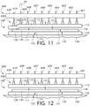
- FIGS. 9-11 illustrate exemplary methods of propagating a first debond front by sequentially applying a plurality of lifting forces to the first carrier at a corresponding plurality of sequential lifting locations of the first carrier in accordance with embodiments of the disclosure
- FIG. 12 illustrates exemplary methods of propagating the first debond front of FIGS. 9-11 until the first carrier is completely separated from the substrate in accordance with embodiments of the disclosure
- FIGS. 13-15 illustrate exemplary methods of propagating a second debond front by sequentially applying a plurality of lifting forces to the second carrier at a corresponding plurality of sequential lifting locations of the second carrier after completely separating the first carrier from the substrate as illustrated in FIG. 12 in accordance with embodiments of the disclosure;
- FIG. 16 illustrates exemplary methods of propagating the second debond front of FIGS. 13-15 until the second carrier is completely separated from the substrate in accordance with embodiments of the disclosure.
- the substrate may be bonded to a carrier. Relative to the substrate, characteristics and size of the carrier may allow the bonded substrate to be handled and transported during processing without significant bending of the substrate that may damage the substrate and/or damage components that may be mounted to the substrate.
- the substrate of any of the embodiments of the disclosure may include a single substrate or a stack of two or more single substrates.
- the single substrates may have a thickness of from about 50 microns to about 300 microns, and all ranges and sub-ranges between the foregoing, although other thicknesses may be provided in some embodiments.
- a single flexible glass substrate or a stack of single flexible glass substrates may be removably bonded to a carrier using a binding agent, for example a polymer binding agent, silicone binding agents, forces naturally generated between one or more roughened abutting surfaces or other binding agents.
- the substrate may be bonded to a carrier fabricated from glass, resin or other materials capable of withstanding conditions during processing of the substrate.
- the carrier may therefore optionally introduce a desired level of rigidity by providing a carrier with additional thickness that is combined with the thickness of the substrate removably bonded to the carrier.
- the carrier may include a plate (e.g., rigid plate) with a thickness that is greater than the thickness of the single substrate bonded to the carrier.
- the carrier may be selected to include a thickness where the overall thickness of the carrier and the substrate bonded to the carrier is within a range that may be employed with processing machinery and equipment configured to process relatively thick glass substrates having a thickness within the range of the overall thickness of the carrier and the substrate bonded to the carrier.
- the carrier After bonding the substrate to the carrier, there may be a desire to remove the carrier from the substrate without damaging the substrate. For example, prior to processing the single substrate (e.g., by adding one or more functional components), there may be a desire to remove the single substrate from the carrier. Alternatively, in some embodiments, there may be a desire to remove the single substrate from the carrier after the substrate has been processed into a single substrate with one or more functional components and prior to creating the substrate as a stack of single substrates. Additionally, in some embodiments, there may be a desire to remove the carrier from the substrate including the stack of single substrates. Accordingly, irrespective of the particular configuration of the substrate, there may be a desire to eventually remove one or more carriers from the substrate.
- the substrate Due to the delicate nature of the substrate, in some embodiments, there may be a desire to remove one of the carriers from the substrate without contacting the substrate, and then to remove the other carrier from the substrate. For example, in some embodiments, there may be a desire to initiate debonding at a predetermined location of an outer peripheral bonded interface between the substrate and the carrier. Such debonding initiation may reduce stress, and may reduce or eliminate possible resulting damage to the substrate and/or to the carrier that may otherwise occur without a debonding initiation step.
- providing a debonding initiation step may target a relatively small location of the outer peripheral bonded interface to allow initial debonding over a small area with a first force, thereby providing a point of weakness in the bond between the substrate and the carrier that may allow easier complete removal (e.g., by peeling) of the carrier from the substrate with a second force that, in some embodiments, may be reduced compared to the first force.
- the initiation area may be extended across a portion of or an entire dimension of the substrate and/or carrier before peeling.
- an apparatus 100 may include a first carrier 110 , a second carrier 120 , and a substrate 130 .
- the first carrier 110 may include a first major surface 111 and an opposing second major surface 112 with a thickness “t 1 ” of the first carrier 110 defined from the first major surface 111 to the second major surface 112 .
- the second carrier 120 may include a first major surface 121 and an opposing second major surface 122 with a thickness “t 2 ” of the second carrier 120 defined from the first major surface 121 to the second major surface 122 .
- the substrate 130 may include a first major surface 131 and an opposing second major surface 132 with a thickness “t 3 ” of the substrate 130 defined from the first major surface 131 to the second major surface 132 .
- At least one of the thickness “t 1 ” of the first carrier 110 and the thickness “t 2 ” of the second carrier 120 may be from about 200 microns to about 700 microns; however, in some embodiments, at least one of the thickness “t 1 ” of the first carrier 110 and the thickness “t 2 ” of the second carrier 120 , may be greater than or less than the explicit dimensions provided in disclosure without departing from the scope of the disclosure.
- the first major surface 111 of the first carrier 110 may face the first major surface 121 of the second carrier 120 (e.g., with the substrate 130 removably bonded between the facing first major surfaces 111 , 121 ).
- the first major surface 131 of the substrate 130 may be removably bonded to the first major surface 111 of the first carrier 110 and the second major surface 132 of the substrate 130 may be removably bonded to the first major surface 121 of the second carrier 120 .
- the substrate 130 may include a first sheet 141 and a second sheet 142 although a single sheet or three or more sheets may be provided in further embodiments. Additionally, in some embodiments, the substrate 130 may include at least one of glass and silicon. For example, in some embodiments, at least one of the first sheet 141 and the second sheet 142 may include a sheet of at least one of glass and silicon. As shown, in some embodiments, the first major surface 131 of the substrate 130 may be defined by an outer surface of the first sheet 141 , and the second major surface 132 of the substrate 130 may be defined by an outer surface of the second sheet 142 . Additionally, an inner surface 133 of the first sheet 141 may be bonded to an inner surface 134 of the second sheet 142 at an interface wall 145 .
- the interface wall 145 may comprise a single wall although the interface wall 145 may comprise a plurality of wall portions or other components in further embodiments.
- the interface wall 145 may comprise an inner interface wall portion and an outer interface wall portion circumscribing the inner interface wall portion.
- a thickness “t 4 ” of the first sheet 141 defined from the outer surface 131 to the inner surface 133 may be from about 50 microns to about 300 microns.
- a thickness “t 5 ” of the second sheet 142 defined from the outer surface 132 to the inner surface 134 may be from about 50 microns to about 300 microns.
- an outer portion 135 of the substrate 130 may be disposed between an outer portion 115 of the first carrier 110 and an outer portion 125 of the second carrier 120 .
- an outer portion 143 of the first sheet 141 and an outer portion 144 of the second sheet 142 may be disposed between the outer portion 115 of the first carrier 110 and the outer portion 125 of the second carrier 120 .
- the first sheet 141 may be removably bonded to the first carrier 110 to provide a first bonded structure 113 .
- the second sheet 142 may be removably bonded to the second carrier 120 to provide a second bonded structure 123 .
- the first bonded structure 113 may be processed with machinery and equipment designed to handle a component having one or more features (e.g., a same or similar size) as that of the first bonded structure 113 .
- processing of the first bonded structure 113 may include, for example, adding one or more functional components (e.g., a color filter 305 ) to the inner surface 133 of the first sheet 141 .
- the first sheet 141 may be inflexible based at least on bonding of the relatively flexible first sheet 141 with the relatively rigid first carrier 110 .
- the first sheet 141 when fully debonded from the first carrier 110 , the first sheet 141 may include a thin, flexible glass, the processing, handling, and transport of which may be difficult without at least the additional rigidity provided to the first bonded structure 113 from the first carrier 110 .
- the second bonded structure 123 may be processed with machinery and equipment designed to handle a component having one or more features (e.g., a same or similar size) as that of the second bonded structure 123 .
- processing of the second bonded structure 123 may include, for example, adding one or more functional components (e.g., thin-film transistor (TFT) components 310 ) to the inner surface 134 of the second sheet 142 to create the second sheet 142 .
- the second sheet 142 may be inflexible based at least on bonding of the relatively flexible second sheet 142 with the relatively rigid second carrier 120 .
- the second sheet 142 may include a thin, flexible glass, the processing, handling, and transport of which may be difficult without at least the additional rigidity provided to the second bonded structure 123 from the second carrier 120 .
- the substrate 130 may be inflexible based at least on bonding of the relatively flexible substrate 130 with the relatively rigid first carrier 110 and second carrier 120 .
- the substrate 130 when fully debonded from the first carrier 110 and the second carrier 120 , the substrate 130 may include a thin, flexible glass panel for display applications, the processing, handling, and transport of which may be difficult without at least the additional rigidity provided to the substrate 130 from the first carrier 110 and/or the second carrier 120 .
- the apparatus 100 may reduce chipping, cracking, scratching, scuffing, abrading, bending, breaking, or other damage to the substrate 130 that may otherwise occur if the substrate 130 was to be processed, handled, and transported without being removably bonded to at least one of the first carrier 110 and the second carrier 120 . Accordingly, the apparatus 100 may also improve processing, handling, and transport of the substrate 130 to provide a more efficient method of processing the substrate 130 than, for example, processing the substrate 130 without removably bonding the substrate 130 to at least one of the first carrier 110 and the second carrier 120 .
- the apparatus 100 may provide characteristics that facilitate initiation of debonding between the substrate 130 and at least one of the first carrier 110 and the second carrier 120 as well as characteristics that facilitate complete separation of at least one of the first carrier 110 and the second carrier 120 from the substrate 130 by propagating a debond front.
- FIG. 4 and FIG. 5 An exemplary method of processing the apparatus 100 is schematically illustrated in FIG. 4 and FIG. 5 which provide alternative views of the enlarged view of the apparatus 100 shown in FIG. 3 .
- the substrate 130 is schematically illustrated in FIG. 4 and FIG. 5 without depicting certain features including the first sheet 141 , the second sheet 142 , and the interface wall 145 shown in FIG. 3 .
- the apparatus 100 is shown with an optional vacuum device 150 including a plate 151 to which the apparatus 100 may be releasably secured. For example, as shown in FIG. 1 and FIG.
- the vacuum device 150 may include a vacuum plate 151 that may include one or more vacuum ports 152 that open at a surface 153 (e.g., a substantially planar surface) of the vacuum plate 151 .
- the one or more vacuum ports 152 may be in selective fluid communication with a vacuum source 205 (shown in FIG. 2 ) for example a vacuum tank or a vacuum pump.
- a vacuum conduit 206 for example a flexible hose, may provide fluid communication between the one or more vacuum ports 152 and the vacuum source 205 .
- a vacuum chamber 210 may be in fluid communication with the one or more vacuum ports 152 such that the one or more vacuum ports 152 are in fluid communication with the vacuum conduit 206 and the vacuum source 205 . Accordingly, the vacuum device 150 may be employed to releasably secure the apparatus 100 (e.g., the first carrier 110 , the second carrier 120 , the substrate 130 ) in place relative to the plate 151 .
- the plate 151 may include a rigid structure made out of metal (e.g., stainless steel, aluminum, etc.), plastic, resin or other material that may substantially resist bending under an applied bending moment. Accordingly, when the apparatus 100 is releasably secured to the plate 151 , in some embodiments, the plate 151 may likewise impart rigidity to the apparatus 100 . Based on the imparted rigidity from the plate 151 , in some embodiments, one or more of the first carrier 110 , the second carrier 120 , and the substrate 130 may also substantially resist bending under an applied bending moment.
- metal e.g., stainless steel, aluminum, etc.
- releasably securing the apparatus 100 to the plate 151 may also allow one to reasonably control, and therefore predict, which of the first carrier 110 and the second carrier 120 will release from the substrate 130 .
- bending of the apparatus 100 may be primarily limited to the first carrier 110 .
- bending of the apparatus 100 may be primarily limited to the second carrier 120 .
- bending of the apparatus 100 may be primarily limited to the remaining first carrier 110 or the remaining second carrier 120 .
- one or more standoffs may also be provided to prevent actual engagement between a surface of the apparatus 100 and the surface 153 of the plate 151 .
- the standoffs may include a peripheral standoff, for example a ring circumscribing the one or more vacuum ports 152 .
- the standoffs may include pillars distributed between one or more vacuum ports 152 throughout the pattern of vacuum ports 152 .
- the pillars may include various materials, for example, a polymeric material.
- the standoffs may extend a distance of about 1.6 mm (e.g., 1/16 of an inch) although other distances may be used in further embodiments.
- releasably securing the apparatus 100 to the plate 151 may be achieved without a vacuum source 205 and may include adhesive bonding or other techniques.
- a tool 170 may be employed to initiate debonding of at least one of the first carrier 110 and the second carrier 120 from the substrate 130 .
- the tool 170 may be inserted in a direction 175 toward a rounded corner 171 of the substrate 130 .
- the tool 170 may be inserted toward a chamfered corner 172 of the substrate 130 .
- the tool 170 may be inserted toward a chamfered corner 173 of at least one of the first carrier 110 and the second carrier 120 or toward a rounded corner 174 of at least one of the first carrier 110 and the second carrier 120 .
- one or more corners of the first carrier 110 , the second carrier 120 , and the substrate 130 may include a rounded corner, a chamfered corner, or other shape corner, without departing from the scope of the disclosure.
- the tool 170 may be employed to engage at least one of the first carrier 110 and the second carrier 120 to impart a force on the at least one of the first carrier 110 and the second carrier 120 . Accordingly, in some embodiments, based at least on the force imparted on the at least one of the first carrier 110 and the second carrier 120 , the tool 170 may be employed to initiate debonding of the at least one of the first carrier 110 and the second carrier 120 from the substrate 130 . In some embodiments, the tool 170 may include a wedge (not shown) to engage at least one of the first carrier 110 and the second carrier 120 to impart a force on the at least one of the first carrier 110 and the second carrier 120 .
- the wedge may be employed to pry the at least one of the first carrier 110 and the second carrier 120 from the substrate 130 .
- the tool 170 may include a rotatable wheel (not shown) having a high coefficient of friction on an outer surface of the wheel.
- the rotatable wheel may be employed to engage at least one of the first carrier 110 and the second carrier 120 to impart a force on the at least one of the first carrier 110 and the second carrier 120 .
- the rotatable wheel may be employed to pry the at least one of the first carrier 110 and the second carrier 120 from the substrate 130 .
- the method may include initiating debonding at the first location 400 of the outer peripheral bonded interface between the substrate 130 and the first carrier 110 by applying a force “F 1 ” to the outer portion 115 of the first carrier 110 to separate a portion of the first carrier 110 from the substrate 130 .
- the force “F 1 ” may be applied to the outer portion 115 of the first carrier 110 without contacting any part of the substrate 130 .
- Preventing any contact with the substrate 130 may avoid direct application of force to the substrate 130 , thereby reducing probability of damaging the substrate 130 that might otherwise occur with other techniques that may directly contact at least one of the substrate 130 and the first carrier 110 with an object (e.g., a blade, a wedge, a friction wheel) in an attempt to break the outer peripheral bonded interface.
- an object e.g., a blade, a wedge, a friction wheel
- the method may include inhibiting bending of the second carrier 120 while applying the force “F 1 ” to the outer portion 115 of the first carrier 110 .
- inhibiting bending of the second carrier 120 may include removably attaching the second major surface 122 of the second carrier 120 to the plate 151 to inhibit bending of the second carrier 120 while applying the force “F 1 ” to the outer portion 115 of the first carrier 110 .
- inhibiting bending of the second carrier 120 may encourage debonding to initiate at the first location 400 of the outer peripheral bonded interface between the substrate 130 and the first carrier 110 .
- the method may include initiating further debonding between the substrate 130 and the first carrier 110 to completely separate the first carrier 110 from the substrate 130 .
- a debonding device 600 (shown in FIG. 6 ) may be employed to apply at least one of a lifting force and a peeling force to the first carrier 110 relative to the substrate 130 to propagate a debond front and debond the first major surface 111 of the first carrier 110 from the first major surface 131 of the substrate 130 thereby completely separating the first carrier 110 from the substrate 130 .
- lifting and “peeling” are not intended to imply a particular orientation of features of the debonding device 600 relative to the direction of gravity. Rather, in one embodiment, “lifting” may be defined as a force or motion occurring in a direction substantially perpendicular to a major surface of one or more of the first carrier 110 , the second carrier 120 , and the substrate 130 irrespective of the direction of gravity. Likewise, “peeling” may be defined as a force or motion occurring in a direction substantially parallel to a major surface of one or more of the first carrier 110 , the second carrier 120 , and the substrate 130 irrespective of the direction of gravity.
- the debonding device 600 may be positioned at an orientation relative to the direction of gravity such that a major surface of one or more of the first carrier 110 , the second carrier 120 , and the substrate 130 is substantially horizontal (e.g., perpendicular to the direction of gravity). Accordingly, lifting may therefore occur in a substantially vertical direction (e.g., parallel and opposite to the direction of gravity) and peeling may therefore occur in a substantially horizontal direction (e.g., perpendicular to the direction of gravity).
- the debonding device 600 may be positioned at an orientation relative to the direction of gravity such that a major surface of one or more of the first carrier 110 , the second carrier 120 , and the substrate 130 is oriented at a substantially non-perpendicular angle relative to the direction of gravity. Accordingly, lifting may therefore occur in a direction substantially perpendicular to a major surface of one or more of the first carrier 110 , the second carrier 120 , and the substrate 130 having an orientation at a substantially non-zero angle relative to the direction of gravity. Likewise, peeling may therefore occur in a direction substantially parallel to a major surface of one or more of the first carrier 110 , the second carrier 120 , and the substrate 130 having an orientation at a substantially non-perpendicular angle relative to the direction of gravity.
- the method may then include initiating debonding at the second location 500 of the outer peripheral bonded interface between the substrate 130 and the second carrier 120 by applying a force “F 2 ” to the second carrier 120 to separate a portion of the second carrier 120 from the substrate 130 .
- the force “F 2 ” may be applied to the outer portion 125 of the second carrier 120 .
- the method may include inhibiting bending of the substrate 130 while applying the force “F 2 ” to the outer portion 125 of the second carrier 120 .
- inhibiting bending of the substrate 130 may include removably attaching the first major surface 131 of the substrate 130 to a plate 151 to inhibit bending of the substrate 130 while applying the force “F 2 ” to the outer portion 125 of the second carrier 120 .
- the apparatus 100 may be flipped over to provide the substrate 130 facing the plate 151 with the second carrier 120 provided to be debonded from the substrate 130 .
- inhibiting bending of the substrate 130 may encourage debonding to initiate at the second location 500 of the outer peripheral bonded interface between the substrate 130 and the second carrier 120 .
- the method may include initiating further debonding between the substrate 130 and the second carrier 120 to completely separate the second carrier 120 from the substrate 130 .
- the debonding device 600 (shown in FIG. 6 ) may be employed to apply at least one of a lifting force and a peeling force to the second carrier 120 relative to the substrate 130 to propagate a debond front and debond the first major surface 121 of the second carrier 120 from the second major surface 132 of the substrate 130 thereby completely separating the second carrier 120 from the substrate 130 .
- initiating debonding between the first carrier 110 and the substrate 130 may be conducted prior to initiating debonding between the second carrier 120 and the substrate 130 .
- initiating further debonding between the first carrier 110 and the substrate 130 may be conducted after initiating debonding between first carrier 110 and the substrate 130 and prior to or after initiating debonding of the second carrier 120 from the substrate 130 as well as prior to or after initiating further debonding of the second carrier 120 from the substrate 130 .
- initiating further debonding between the second carrier 120 and the substrate 130 may be conducted after initiating debonding between second carrier 120 and the substrate 130 and prior to or after initiating debonding of the first carrier 110 from the substrate 130 as well as prior to or after initiating further debonding of the first carrier 110 from the substrate 130 .
- completely separating the first carrier 110 from the substrate 130 may be conducted prior to or after one or more of initiating debonding of the second carrier 120 from the substrate 130 , initiating further debonding of the second carrier 120 from the substrate 130 , and completely separating the second carrier 120 from the substrate 130 .
- completely separating the second carrier 120 from the substrate 130 may be conducted prior to or after one or more of initiating debonding of the first carrier 110 from the substrate 130 , initiating further debonding of the first carrier 110 from the substrate 130 , and completely separating the first carrier 110 from the substrate 130 .
- a setback lateral distance “d 1 ” may define a distance between an outer peripheral edge 136 of the outer portion 135 of the substrate 130 and at least one of an outer peripheral edge 117 of the outer portion 115 of the first carrier 110 and an outer peripheral edge 127 of the outer portion 125 of the second carrier 120 .
- the outer peripheral edge 136 of the outer portion 135 of the substrate 130 may be defined by an outermost feature of at least one of an outer peripheral edge 147 of the outer portion 143 of the first sheet 141 and an outer peripheral edge 148 of the outer portion 144 of the second sheet 142 .
- the setback lateral distance “d 1 ” may define a dimension from the outer peripheral edge 136 of the outer portion 135 of the substrate 130 to a location at which a force to initiate debonding of at least one of the first carrier 110 from the substrate 130 and the second carrier 120 from the substrate 130 is applied.
- a force “F 1 ” may be applied to the first carrier 110 to initiate debonding of the first carrier 110 from the substrate 130 at the first location 400 of an outer peripheral bonded interface between the substrate 130 and the first carrier 110 .
- the setback lateral distance “d 1 ” multiplied by the force “F 1 ” may define a bending moment applied to the outer peripheral bonded interface between the substrate 130 and the first carrier 110 at the first location 400 .
- a force “F 2 ” may be applied to the second carrier 120 to initiate debonding of the second carrier 120 from the substrate 130 at the second location 500 of an outer peripheral bonded interface between the substrate 130 and the second carrier 120 .
- the setback lateral distance “d 1 ” multiplied by the force “F 2 ” may define a bending moment applied to the outer peripheral bonded interface between the substrate 130 and the second carrier 120 at the second location 500 .
- an offset lateral distance “d 2 ” may be defined between the outer peripheral edge 136 of the outer portion 135 of the substrate 130 and an outer peripheral edge 146 of the interface wall 145 .
- the offset lateral distance “d 2 ” may provide the interface wall 145 spaced at a predetermined dimension from the outer peripheral edge 136 of the substrate 130 .
- the interface wall 145 may provide a strong, permanent bond between the first sheet 141 and the second sheet 142 without features of the interface wall 145 contacting or interfering with the first carrier 110 and the second carrier 120 .
- the interface wall 145 may include an epoxy.
- the interface wall 145 may include a frit including glass (e.g., sintered frit).
- the offset lateral distance “d 2 ” may be constant relative to a boundary extending around a periphery of the substrate 130 ; or the offset lateral distance “d 2 ” may vary relative to the boundary extending around a periphery of the substrate 130 .
- a debonding device 600 may include a plurality of suction cups 650 .
- each suction up (e.g., suction cup 651 ) of the plurality of suction cups 650 may be attached to a corresponding shaft (e.g., shaft 652 ).
- the debonding device 600 may include a frame 620 to which each shaft 652 of the plurality of suction cups 650 may be operably connected.
- a controller 625 may be provided to communicate via one or more communication lines 630 with the plurality of suction cups 650 .
- the controller 625 may include any one or more of a microcontroller, programmable logic controller (PLC), discrete controller, circuit, computer, or other mechanical or electronic control feature including an active or passive user interface by which a robot or human user may select, adjust, start, stop, or otherwise control the one or more operations of the debonding device 600 including, but not limited to, a timing (e.g., sequential timing) operation of any one or more of the plurality of suction cups 650 .
- the debonding device 600 may be partially or entirely manually operated with or without a controller.
- the controller 625 may independently operate one or more features of one or more of the plurality of suction cups 650 .
- the controller 625 may independently operate a vacuum function of one or more of the plurality of suction cups 650 to provide a suction force from one or more of the plurality of suction cups 650 .
- any of the suction cups of the plurality of suction cups 650 may be independently operable to releasably engage and/or disengage, for example, at least one of the first carrier 110 and the second carrier 120 .
- the controller 625 may independently operate a mechanical function of one or more of the plurality of suction cups 650 to independently move (e.g., at least one of raise and lower) one or more of the plurality of suction cups 650 . Accordingly, in some embodiments, any of the suction cups of the plurality of suction cups 650 may be independently operable to move relative to at least one of the first carrier 110 and the second carrier 120 .
- the plurality of suction cups 650 may be arranged in rows (e.g., first row 601 , second row 602 , third row 603 , fourth row 604 , fifth row 605 , sixth row 606 , seventh row 607 , eighth row 608 , ninth row 609 , tenth row 610 ).
- one or more rows of suction cups of the plurality of suction cups 650 may be independently operable to releasably engage and/or disengage, for example, at least one of the first carrier 110 and the second carrier 120 .
- one or more rows of suction cups of the plurality of suction cups 650 may be independently operable to move relative to at least one of the first carrier 110 and the second carrier 120 .
- the particular number of suction cups of the plurality of suction cups 650 as well as the particular number of rows of suction cups are not intended to limit the disclosure. Accordingly, in some embodiments, the debonding device 600 may be modified in accordance with embodiments of the disclosure to include any number of suction cups as well as any number of rows of suction cups without departing from the scope of the disclosure. In some embodiments, the particular number of suction cups of the plurality of suction cups 650 as well as the particular number of rows of suction cups may be based on, for example, one or more of the size of the apparatus 100 , the vacuum force desired to be provided from the debonding device 600 , and the size or other characteristic features of the suction cups.
- one or more suction cups of the plurality of suction cups 650 may be compliant to, for example, flex when engaged with at least one of the first carrier 110 and the second carrier 120 .
- one or more suction cups of the plurality of suction cups 650 may move (e.g., at least one of raise and lower) in a vertical direction (e.g., along an axis of a respective shaft 652 ) perpendicular to a major surface of at least one of the first carrier 110 and the second carrier 120 and may also flex about an axis perpendicular to the vertical direction.
- one or more suction cups of the plurality of suction cups 650 may be pivotable relative to at least one of the first carrier 110 and the second carrier 120 .
- one or more suction cups of the plurality of suction cups 650 may move (e.g., at least one of raise and lower) in the vertical direction perpendicular to a major surface of at least one of the first carrier 110 and the second carrier 120 and also be pivotable about an axis perpendicular to the vertical direction.
- a resilient or pivotable suction cup may, in some embodiments, reduce the likelihood of causing stress concentrations in one or more of the first carrier 110 , the second carrier 120 , and the substrate 130 that may otherwise occur, for example, when engaging at least one of the first carrier 110 and the second carrier 120 with a substantially non-compliant (e.g., rigid) suction cup or a suction cup that resists pivoting relative to the at least one of the first carrier 110 and the second carrier 120 .
- one or more suction cups of the plurality of suction cups 650 may be modified in accordance with embodiments of the disclosure to include a variety of shapes and other characteristic features without departing from the scope of the disclosure.
- a method of processing the substrate 130 may include propagating a first debond front (e.g., first debond front 900 , 1000 , 1100 ) from a first debonded location (e.g., first location 400 , shown in FIG. 4 ) along a first direction 700 (shown in FIG. 7 and FIG. 8 ) extending away from the first debonded location 400 .
- FIG. 7 provides a schematic view of the debonding device 600 taken along line 7 - 7 of FIG. 6
- FIG. 8 provides an alternate embodiment of the debonding device 600 of FIG. 7 .
- the first debond front 900 , 1000 , 1100 may be defined as the location between the first major surface 111 of the first carrier 110 and the first major surface 131 of the substrate 130 at which the bond which removably bonds the first major surface 111 of the first carrier 110 to the first major surface 131 of the substrate 130 transitions from debonded (e.g., behind the first debond front 900 , 1000 , 1100 relative to the first direction 700 of propagation) to bonded (e.g., in front of the first debond front 900 , 1000 , 1100 relative to the first direction 700 of propagation). Accordingly, as the first carrier 110 is peeled away from the substrate 130 , the first debond front may sequentially propagate along the first direction 700 .
- the method of processing the substrate 130 may include continuously propagating the first debond front 900 , 1000 , 1100 without ceasing propagation of the first debond front 900 , 1000 , 1100 until the first carrier 110 is completely separated from the substrate 130 .
- the method of processing the substrate 130 may include propagating the first debond front 900 , 1100 , 1100 by sequentially applying a plurality of lifting forces to the first carrier 110 at a corresponding plurality of first sequential lifting locations (e.g., first sequential lifting location 671 , second sequential lifting location 672 , third sequential lifting location 673 , fourth sequential lifting location 674 , fifth sequential lifting location 675 , sixth sequential lifting location 676 , seventh sequential lifting location 677 , eighth sequential lifting location 678 , ninth sequential lifting location 679 , tenth sequential lifting location 680 , shown in FIG. 6 ) of the first carrier 110 .
- first sequential lifting location 671 , second sequential lifting location 672 , third sequential lifting location 673 , fourth sequential lifting location 674 , fifth sequential lifting location 675 , sixth sequential lifting location 676 , seventh sequential lifting location 677 , eighth sequential lifting location 678 , ninth sequential lifting location 679 , tenth sequential lifting location 680 , shown in FIG. 6 of the first carrier 110 .
- each lifting force of the plurality of lifting forces may be sequentially applied at a corresponding lifting location of the plurality of first sequential lifting locations after the first debond front 900 , 1000 , 1100 has propagated past the corresponding lifting location of the first carrier 110 .
- FIGS. 9-11 illustrate exemplary methods of propagating the first debond front 900 , 1000 , 1100 by sequentially applying a plurality of lifting forces to the first carrier 110 at the corresponding plurality of first sequential lifting locations 671 , 672 , 673 , 674 , 675 , 676 , 677 , 678 , 679 , 680 of the first carrier 110 .
- FIG. 7 and FIG. 8 To schematically illustrate a dynamic propagation of the first debond front, three representative moments in time of the continuous propagation of the first debond front are illustrated simultaneously in FIG. 7 and FIG. 8 with the understanding that each representative moment in time occurs at a discrete moment in time during the continuous propagation of the first debond front as illustrated individually in FIGS. 9-11 .
- FIG. 9-11 illustrate exemplary methods of propagating the first debond front 900 , 1000 , 1100 by sequentially applying a plurality of lifting forces to the first carrier 110 at the corresponding plurality of first sequential lifting locations 671 , 672 , 673
- FIG. 9 illustrates the first debond front 900 at a first discrete moment in time
- FIG. 10 illustrates the first debond front 1000 at a second discrete moment in time occurring after the first discrete moment in time of FIG. 9
- FIG. 11 illustrates the first debond front 1100 at a third discrete moment in time occurring after the second discrete moment in time of FIG. 10
- FIG. 12 illustrates exemplary methods of propagating the first debond front 900 , 1000 , 1100 of FIGS. 9-11 until the first carrier 110 is completely separated from the substrate 130 .
- FIG. 12 illustrates the method of processing the substrate 130 at a fourth discrete moment in time occurring after the third discrete moment in time of FIG. 11 .
- the first location 400 of the outer peripheral bonded interface between the substrate 130 and the first carrier 110 may include a corner portion of the substrate 130 where debonding between the substrate 130 and the first carrier 110 has been initiated (e.g., as shown in FIG. 4 ).
- the corner portion of the substrate 130 may be defined between an intersection of a first edge 401 and a second edge 402 of the substrate 130 .
- the first location 400 of the outer peripheral bonded interface between the substrate 130 and the first carrier 110 may be extended (e.g., widened) to include an outer peripheral edge (e.g., the entire first edge 401 ) of the substrate 130 .
- the first direction 700 may extend perpendicular to the outer peripheral edge 401 of the substrate 130 and across the substrate 130 .
- the first direction 700 may extend from the corner portion (e.g., from the intersection of the first edge 401 and the second edge 402 ) of the substrate 130 diagonally across the substrate 130 .
- the method of processing the substrate 130 may include propagating a second debond front (e.g., second debond front 1300 , 1400 , 1500 ) from a second debonded location (e.g., second location 500 , shown in FIG. 5 ) along a second direction 800 (shown in FIG. 7 and FIG. 8 ) extending away from the second debonded location 500 .
- a second debond front e.g., second debond front 1300 , 1400 , 1500
- a second debonded location e.g., second location 500 , shown in FIG. 5
- a second direction 800 shown in FIG. 7 and FIG. 8
- the second debond front 1300 , 1400 , 1500 may be defined as the location between the first major surface 121 of the second carrier 120 and the second major surface 132 of the substrate 130 at which the bond which removably bonds the first major surface 121 of the second carrier 120 to the second major surface 132 of the substrate 130 transitions from debonded (e.g., behind the second debond front 1300 , 1400 , 1500 relative to the second direction 800 of propagation) to bonded (e.g., in front of the second debond front 1300 , 1400 , 1500 relative to the second direction 800 of propagation). Accordingly, as the second carrier 120 is peeled away from the substrate 130 , the second debond front may sequentially propagate along the second direction 800 .
- the method of processing the substrate 130 may include continuously propagating the second debond front 1300 , 1400 , 1500 without ceasing propagation of the second debond front 1300 , 1400 , 1500 until the second carrier 120 is completely separated from the substrate 130 .
- the method of processing the substrate 130 may include propagating the second debond front 1300 , 1400 , 1500 by sequentially applying a plurality of lifting forces to the second carrier 120 at a corresponding plurality of second sequential lifting locations (e.g., first sequential lifting location 681 , second sequential lifting location 682 , third sequential lifting location 683 , fourth sequential lifting location 684 , fifth sequential lifting location 685 , sixth sequential lifting location 686 , seventh sequential lifting location 687 , eighth sequential lifting location 688 , ninth sequential lifting location 689 , tenth sequential lifting location 690 , shown in FIG. 13 ) of the second carrier 120 .
- second sequential lifting locations e.g., first sequential lifting location 681 , second sequential lifting location 682 , third sequential lifting location 683 , fourth sequential lifting location 684 , fifth sequential lifting location 685 , sixth sequential lifting location 686 , seventh sequential lifting location 687 , eighth sequential lifting location 688 , ninth sequential lifting location 689 , tenth sequential lifting location 690 , shown in FIG. 13
- each lifting force of the plurality of lifting forces may be sequentially applied at a corresponding lifting location of the second plurality of sequential lifting locations after the second debond front 1300 , 1400 , 1500 has propagated past the corresponding lifting location of the second carrier 120 .
- FIGS. 13-15 illustrate exemplary methods of propagating the second debond front 1300 , 1400 , 1500 by sequentially applying a plurality of lifting forces to the second carrier 120 at the corresponding plurality of second sequential lifting locations 681 , 682 , 683 , 684 , 685 , 686 , 687 , 688 , 689 , 690 of the second carrier 120 .
- FIG. 7 and FIG. 8 Three representative moments in time of the continuous propagation of the second debond front are illustrated simultaneously in FIG. 7 and FIG. 8 with the understanding that each representative moment in time occurs at a discrete moment in time during the continuous propagation of the second debond front as illustrated individually in FIGS. 13-15 .
- FIG. 13-15 illustrate exemplary methods of propagating the second debond front 1300 , 1400 , 1500 by sequentially applying a plurality of lifting forces to the second carrier 120 at the corresponding plurality of second sequential lifting locations 681 , 682 , 683 , 684 , 685 , 686 , 687
- FIG. 13 illustrates the second debond front 1300 at a first discrete moment in time
- FIG. 14 illustrates the second debond front 1400 at a second discrete moment in time occurring after the first discrete moment in time of FIG. 13
- FIG. 15 illustrates the second debond front 1500 at a third discrete moment in time occurring after the second discrete moment in time of FIG. 14
- FIG. 16 illustrates exemplary methods of propagating the second debond front 1300 , 1400 , 1500 of FIGS. 13-15 until the second carrier 120 is completely separated from the substrate 130 .
- FIG. 16 illustrates the method of processing the substrate 130 at a fourth discrete moment in time occurring after the third discrete moment in time of FIG. 15 .
- the second location 500 of the outer peripheral bonded interface between the substrate 130 and the second carrier 120 may include a corner portion of the substrate 130 where debonding between the substrate 130 and the second carrier 120 has been initiated (e.g., as shown in FIG. 5 ).
- the corner portion of the substrate 130 may be defined between an intersection of the first edge 401 and the second edge 402 of the substrate 130 .
- the second location 500 of the outer peripheral bonded interface between the substrate 130 and the second carrier 120 may be extended (e.g., widened) to include an outer peripheral edge (e.g., the entire first edge 401 ) of the substrate 130 .
- the second direction 800 may extend perpendicular to the outer peripheral edge 401 of the substrate 130 and across the substrate 130 .
- the second direction 800 may extend from the corner portion (e.g., from the intersection of the first edge 401 and the second edge 402 ) of the substrate 130 diagonally across the substrate 130 .
- propagating at least one of the first debond front 900 , 1000 , 1100 and the second debond front 1300 , 1400 , 1500 diagonally across the substrate 130 may provide a smoother (e.g., more fluid) propagation of the respective debond front than, for example, propagating at least one of the first debond front 900 , 1000 , 1100 and the second debond front 1300 , 1400 , 1500 perpendicular to the outer peripheral edge 401 across the substrate 130 .
- propagating at least one of the first debond front 900 , 1000 , 1100 and the second debond front 1300 , 1400 , 1500 diagonally across the substrate 130 may require less force to peel at least one of the first carrier 110 and the second carrier 120 from the substrate 130 than, for example, a comparable force to peel at least one of the first carrier 110 and the second carrier 120 from the substrate 130 when propagating at least one of the first debond front 900 , 1000 , 1100 and the second debond front 1300 , 1400 , 1500 perpendicular to the outer peripheral edge 401 across the substrate 130 .
- a bending stiffness of the substrate 130 may be nonuniform and may vary depending on a localized stiffness of the substrate 130 at one or more localized locations of the substrate 130 .
- the interface wall 145 may alter or control a localized stiffness of the substrate 130 , such that, depending on an orientation of the substrate 130 relative to an applied bending moment, the bending stiffness of the substrate 130 may be nonuniform. Propagating at least one of the first debond front 900 , 1000 , 1100 and the second debond front 1300 , 1400 , 1500 diagonally across the substrate 130 may accommodate (e.g., compensate) for the nonuniform bending stiffness of the substrate 130 .
- the interface wall 145 may extend along a peripheral boundary of the substrate 130 ; and, in some embodiments, at least a portion of the peripheral boundary may extend substantially parallel to the direction of propagation of the debond front when the debond front is propagated perpendicular to the outer peripheral edge 401 across the substrate 130 .
- the substantially parallel alignment of the at least a portion of the peripheral boundary of the interface wall 145 and the direction of propagation perpendicular to the outer peripheral edge 401 across the substrate 130 may, in some embodiments, stall or interrupt propagation of the debond front.
- a peeling force to debond at least one of the first carrier 110 and the second carrier 120 from the substrate 130 may be increased.
- the likelihood of damaging one or more of the first carrier 110 , the second carrier 120 , and the substrate 130 may also increase.
- applying a force to debond at least one of the first carrier 110 and the second carrier 120 from the substrate 130 to propagate the debond front may stress one or more of the first carrier 110 , the second carrier 120 , and the substrate 130 . Therefore, increased applied forces may result in increased stresses in one or more of the first carrier 110 , the second carrier 120 , and the substrate 130 .
- propagating at least one of the first debond front 900 , 1000 , 1100 and the second debond front 1300 , 1400 , 1500 diagonally across the substrate 130 stalling or interruption of propagation of the debond front may be reduced or eliminated. That is, propagating the debond front diagonally across the substrate 130 may alter the otherwise substantially parallel alignment of the at least a portion of the peripheral boundary of the interface wall 145 and the direction of propagation perpendicular to the outer peripheral edge 401 across the substrate 130 .
- a substantially non-parallel alignment e.g., diagonal alignment
- propagating at least one of the first debond front 900 , 1000 , 1100 and the second debond front 1300 , 1400 , 1500 diagonally across the substrate 130 may reduce and minimize stress of one or more of the first carrier 110 , the second carrier 120 , and the substrate 130 . Therefore, the likelihood of damaging one or more of the first carrier 110 , the second carrier 120 , and the substrate 130 based on applying forces to propagate the debond front may, likewise, also be reduced and minimized.
- propagating at least one of the first debond front 900 , 1000 , 1100 and the second debond front 1300 , 1400 , 1500 diagonally across the substrate 130 may control the debond front to reach a portion of the substrate 130 opposite at least one of the first location 400 and the second location 500 relative to a respective first direction 700 and second direction 800 in a manner that provides a gentler, more controllable complete separation of at least one of the first carrier 110 and the second carrier 120 from the substrate 130 .
- propagating at least one of the first debond front 900 , 1000 , 1100 and the second debond front 1300 , 1400 , 1500 diagonally across the substrate 130 controls the debond front to reach (and propagate along) opposing edges 403 , 404 of the substrate 130 at different times such that peeling and complete separation of at least one of the first carrier 110 and the second carrier 120 from the substrate 130 may be performed in a more controllable, gentler manner, thus reducing the likelihood of stressing and damaging one or more of the first carrier 110 , the second carrier 120 , and the substrate 130 .
- propagating at least one of the first debond front 900 , 1000 , 1100 and the second debond front 1300 , 1400 , 1500 perpendicular to the outer peripheral edge 401 of the substrate 130 across the substrate 130 controls the debond front to reach (and propagate along) opposing edge 403 of the substrate 130 at a substantially instantaneous moment in time.
- attempting to completely separate at least one of the first carrier 110 and the second carrier 120 from the substrate 130 with a final debonding of the entire opposing edge 403 of the substrate 130 occurring substantially instantaneously at a moment in time may result in a sudden and less controllable peeling and complete separation of at least one of the first carrier 110 and the second carrier 120 from the substrate 130 .
- attempting to completely separate at least one of the first carrier 110 and the second carrier 120 from the substrate 130 with a final debonding of the entire opposing edge 403 of the substrate 130 occurring substantially instantaneously at a moment in time may increase the likelihood of stressing and damaging one or more of the first carrier 110 , the second carrier 120 , and the substrate 130 .
- propagating at least one of the first debond front 900 , 1000 , 1100 and the second debond front 1300 , 1400 , 1500 diagonally across the substrate 130 may therefore, in some embodiments, provide a more efficient and more reliable method of processing the substrate 130 than, for example, propagating at least one of the first debond front 900 , 1000 , 1100 and the second debond front 1300 , 1400 , 1500 perpendicular to the outer peripheral edge 401 of the substrate 130 across the substrate 130 (e.g., as shown in FIG. 7 ).
- the rows 601 , 602 , 603 , 604 , 605 , 606 , 607 , 608 , 609 , 610 of suction cups of the plurality of suction cups 650 may be arranged along at least one of the first direction 700 and the second direction 800 .
- the plurality of lifting forces e.g., a lifting force from a respective row of suction cups
- the plurality of lifting forces may be sequentially applied after the first debond front 900 , 1000 , 1100 has propagated past the corresponding lifting location of the first carrier 110 (e.g., when debonding the first carrier 110 from the substrate 130 ) and after the second debond front 1300 , 1400 , 1500 has propagated past the corresponding lifting location of the second carrier 120 (e.g., when debonding the second carrier 120 from the substrate 130 ).
- the plurality of lifting forces e.g., a lifting force from a respective row of suction cups
- the plurality of lifting forces may be sequentially applied at a corresponding lifting location of the first carrier 110 and the second carrier 120 .
- Sequentially applying a respective sequential lifting force at a corresponding lifting location of the first carrier 110 and the second carrier 120 may facilitate debonding between the first carrier 110 and the substrate 130 and the second carrier 120 and the substrate 130 based on peeling of the first carrier 110 relative to the substrate 130 and peeling of the second carrier 120 relative to the substrate 130 .
- peeling as compared to translation (e.g., lifting) of the first carrier 110 away from the substrate 130 and lifting of the second carrier 120 away from the substrate 130 may provide a more controllable propagation of the respective debond front.
- propagating the debond front by peeling may be accomplished with application of relatively smaller forces compared to forces require to propagate the debond front by translation (e.g., lifting).
- the first debond front 900 , 1000 , 1100 may sequentially propagate along the first direction 700 .
- the second debond front 1300 , 1400 , 1500 may sequentially propagate along the second direction 800 .
- the method of processing the substrate 130 may include continuously propagating the first debond front 900 , 1000 , 1100 without ceasing propagation of the first debond front 900 , 1000 , 1100 until the first carrier 110 is completely separated from the substrate 130 .
- the method of processing the substrate 130 may include continuously propagating the second debond front 1300 , 1400 , 1500 without ceasing propagation of the second debond front 1300 , 1400 , 1500 until the second carrier 120 is completely separated from the substrate 130 .
- continuously propagating the debond front without ceasing propagation may reduce the applied force to debond at least one of the first carrier 110 and the second carrier 120 from the substrate 130 .
- the potential (e.g., static) energy bonding the at least one of the first carrier 110 and the second carrier 120 to the substrate 130 is released, and to advance the debond front, propagation may continue by overcoming, for example, dynamic bond energy.
- the propagation of the debond front may be advantageous to continuously propagate the debond front without ceasing propagation of the debond front to avoid having to overcome the potential (e.g., static) energy bonding the at least one of the first carrier 110 and the second carrier 120 to the substrate 130 that is present when the debond front is stationary.
- potential e.g., static
- features of the disclosure may reduce the applied force to debond at least one of the first carrier 110 and the second carrier 120 from the substrate 130 .
- the likelihood of stressing and damaging one or more of the first carrier 110 , the second carrier 120 , and the substrate 130 may likewise be reduced.
- propagating at least one of the first debond front 900 , 1000 , 1100 and the second debond front 1300 , 1400 , 1500 by sequentially applying a lifting force from a respective row of suction cups after the debond front has propagated past the corresponding lifting location and thereby peeling (e.g., continuously peeling without ceasing peeling) at least one of the first carrier 110 and the second carrier 120 from the substrate 130 may, in some embodiments, provide a more efficient and more reliable method of processing the substrate 130 .
- the plurality of suction cups 650 may engage the first carrier 110 (e.g., contact, and provide a suction force) prior to propagating the first debond front 900 , 1000 , 1100 .
- the plurality of suction cups 650 may engage the first carrier 110 , and then the plurality of lifting forces may be sequentially applied by a respective suction cup (e.g., row of suction cups) of the plurality of suction cups 650 after the first debond front 900 , 1000 , 1100 propagates past the respective suction cup and before the first debond front 900 , 1000 , 1100 propagates past an immediately adjacent suction cup (e.g., row of suction cups) of the plurality of suction cups 650 arranged downstream from the respective suction cup along the first direction 700 .
- a respective suction cup e.g., row of suction cups
- the plurality of suction cups 650 may engage the second carrier 120 (e.g., contact, and provide a suction force) prior to propagating the second debond front 1300 , 1400 , 1500 .
- the plurality of suction cups 650 may engage the second carrier 120 , and then the plurality of lifting forces may be sequentially applied by a respective suction cup (e.g., row of suction cups) of the plurality of suction cups 650 after the second debond front 1300 , 1400 , 1500 propagates past the respective suction cup and before the second debond front 1300 , 1400 , 1500 propagates past an immediately adjacent suction cup (e.g., row of suction cups) of the plurality of suction cups 650 arranged downstream from the respective suction cup along the second direction 800 .
- a respective suction cup e.g., row of suction cups
- the method of processing the substrate 130 may include applying a sequential lifting force “F 1 ” to a corresponding sequential lifting location 671 of the first carrier 110 (e.g., by lifting row 601 of the plurality of suction cups 650 ) after the first debond front 900 has propagated past the corresponding sequential lifting location 671 of the first carrier 110 .
- the sequential lifting force “F 1 ” may be applied to the corresponding sequential lifting location 671 of the first carrier 110 after the first debond front 900 has propagated past the corresponding sequential lifting location 671 of the first carrier 110 and before the first debond front 900 propagates past an immediately adjacent suction cup (e.g., row 602 ) of the plurality of suction cups 650 arranged downstream from the respective suction cup row 601 along the propagation direction.
- an immediately adjacent suction cup e.g., row 602
- the method of processing the substrate 130 may further include applying a sequential lifting force “F 4 ” to a corresponding sequential lifting location 674 of the first carrier 110 (e.g., by lifting row 604 of the plurality of suction cups 650 ) after the first debond front 1000 has propagated past the corresponding sequential lifting location 674 of the first carrier 110 .
- the sequential lifting force “F 4 ” may be applied to the corresponding sequential lifting location 674 of the first carrier 110 after the first debond front 1000 has propagated past the corresponding sequential lifting location 674 of the first carrier 110 and before the first debond front 1000 propagates past an immediately adjacent suction cup (e.g., row 605 ) of the plurality of suction cups 650 arranged downstream from the respective suction cup row 604 along the propagation direction.
- an immediately adjacent suction cup e.g., row 605
- the method of processing the substrate 130 may further include applying a sequential lifting force “F 9 ” to a corresponding sequential lifting location 679 of the first carrier 110 (e.g., by lifting row 609 of the plurality of suction cups 650 ) after the first debond front 1100 has propagated past the corresponding sequential lifting location 679 of the first carrier 110 .
- the sequential lifting force “F 9 ” may be applied to the corresponding sequential lifting location 679 of the first carrier 110 after the first debond front 1100 has propagated past the corresponding sequential lifting location 679 of the first carrier 110 and before the first debond front 1100 propagates past an immediately adjacent suction cup (e.g., row 610 ) of the plurality of suction cups 650 arranged downstream from the respective suction cup row 609 along the propagation direction.
- an immediately adjacent suction cup e.g., row 610
- the plurality of suction cups 650 may releasably hold the first carrier 110 once the first debond front 900 , 1000 , 1100 has propagated and the first carrier 110 has completely separated from the substrate 130 . Additionally, in some embodiments, the method of processing the substrate 130 may include inhibiting bending of the second carrier 120 while sequentially applying the plurality of lifting forces (e.g., “F 1 ”, “F 4 ”, “F 9 ”) to the first carrier 110 .
- the plurality of lifting forces e.g., “F 1 ”, “F 4 ”, “F 9 ”
- inhibiting bending of the second carrier 120 may include removably attaching the second major surface 122 of the second carrier 120 to the plate 151 to inhibit bending of the second carrier 120 while sequentially applying the plurality of lifting forces (e.g., “F 1 ”, “F 4 ”, “F 9 ”) to the first carrier 110 .
- the plurality of lifting forces e.g., “F 1 ”, “F 4 ”, “F 9 ”
- the method of processing the substrate 130 may then include applying a sequential lifting force “F 1 ” to a corresponding sequential lifting location 681 of the second carrier 120 (e.g., by lifting row 601 of the plurality of suction cups 650 ) after the second debond front 1300 has propagated past the corresponding sequential lifting location 681 of the second carrier 120 .
- the sequential lifting force “F 1 ” may be applied to the corresponding sequential lifting location 681 of the second carrier 120 after the second debond front 1300 has propagated past the corresponding sequential lifting location 681 of the second carrier 120 and before the second debond front 1300 propagates past an immediately adjacent suction cup (e.g., row 602 ) of the plurality of suction cups 650 arranged downstream from the respective suction cup row 601 along the propagation direction.
- an immediately adjacent suction cup e.g., row 602
- the method of processing the substrate 130 may further include applying a sequential lifting force “F 4 ” to a corresponding sequential lifting location 684 of the second carrier 120 (e.g., by lifting row 604 of the plurality of suction cups 650 ) after the second debond front 1400 has propagated past the corresponding sequential lifting location 684 of the second carrier 120 .
- the sequential lifting force “F 4 ” may be applied to the corresponding sequential lifting location 684 of the second carrier 120 after the second debond front 1400 has propagated past the corresponding sequential lifting location 684 of the second carrier 120 and before the second debond front 1400 propagates past an immediately adjacent suction cup (e.g., row 605 ) of the plurality of suction cups 650 arranged downstream from the respective suction cup row 604 along the propagation direction.
- an immediately adjacent suction cup e.g., row 605
- the method of processing the substrate 130 may further include applying a sequential lifting force “F 9 ” to a corresponding sequential lifting location 689 of the second carrier 120 (e.g., by lifting row 609 of the plurality of suction cups 650 ) after the second debond front 1500 has propagated past the corresponding sequential lifting location 689 of the second carrier 120 .
- the sequential lifting force “F 9 ” may be applied to the corresponding sequential lifting location 689 of the second carrier 120 after the second debond front 1500 has propagated past the corresponding sequential lifting location 689 of the second carrier 120 and before the second debond front 1500 propagates past an immediately adjacent suction cup (e.g., row 610 ) of the plurality of suction cups 650 arranged downstream from the respective suction cup row 609 along the propagation direction.
- an immediately adjacent suction cup e.g., row 610
- the plurality of suction cups 650 may releasably hold the second carrier 120 once the second debond front 1300 , 1400 , 1500 has propagated and the second carrier 120 has completely separated from the substrate 130 .
- the method of processing the substrate 130 may include inhibiting bending of the substrate 130 while sequentially applying the plurality of lifting forces (e.g., “F 1 ”, “F 4 ”, “F 9 ”) to the second carrier 120 .
- inhibiting bending of the substrate 130 may include removably attaching the first major surface 131 of the substrate 130 to the plate 151 to inhibit bending of the substrate 130 while applying the plurality of lifting forces (e.g., “F 1 ”, “F 4 ”, “F 9 ”) to the second carrier 120 .
- the plurality of lifting forces e.g., “F 1 ”, “F 4 ”, “F 9 ”
- the ability of the plate 151 to releasably secure the apparatus 100 may also limit the amount of force that may be applied to at least one of the first carrier 110 and the second carrier 120 .
- an applied force e.g., by the debonding device 600
- a counteracting force that releasably secures the apparatus 100 to the plate 151 may separate the apparatus 100 from the plate 151 prior to propagation (e.g., complete propagation) of the debond front.
- the counteracting force that releasably secures the apparatus 100 to the plate 151 may be selected to provide a threshold relative to the applied force (e.g., by the debonding device 600 ) above which the apparatus 100 will intentionally separate from the plate 151 , for example, prior to one or more of the first carrier 110 , the second carrier 120 , and the substrate 130 breaking.
- the method of processing the substrate 130 may optionally include decreasing bond energy between the substrate 130 and at least one of first carrier 110 and the second carrier 120 based on a thermoelectric effect.
- decreasing bond energy between the substrate 130 and at least one of first carrier 110 and the second carrier 120 may include decreasing a temperature of at least one of first carrier 110 and the second carrier 120 .
- decreasing the temperature of at least one of first carrier 110 and the second carrier 120 reduces the bond energy and, therefore, reduces the strength of the bond such that comparatively smaller forces may be applied (e.g., by the debonding device 600 ) to propagate the debond front than, for example, forces to propagate the debond front without decreasing bond energy between the substrate 130 and at least one of first carrier 110 and the second carrier 120 based on a thermoelectric effect.
- the method of processing the substrate 130 may optionally include decreasing bond energy between the substrate 130 and at least one of first carrier 110 and the second carrier 120 based on a de-ionizing effect.
- decreasing bond energy between the substrate 130 and at least one of first carrier 110 and the second carrier 120 may include neutralizing static generated during debonding of at least one of first carrier 110 and the second carrier 120 from the substrate 130 .
- neutralizing the static generated during debonding reduces the bond energy and, therefore, reduces the strength of the bond such that comparatively smaller forces may be applied (e.g., by the debonding device 600 ) to propagate the debond front than, for example, forces to propagate the debond front without neutralizing the static generated during debonding between the substrate 130 and at least one of first carrier 110 and the second carrier 120 based on a de-ionizing effect.
- bond may refer to any one or more of dynamic shear strength, dynamic peel strength, static shear strength, static peel strength and combinations thereof.
- Peel strength is the force per unit width to initiate failure (e.g. static) and/or to maintain a specified rate of failure (e.g. dynamic) by means of a stress applied to a bonded interface between at least one of the first carrier 110 and the second carrier 120 and the substrate 130 in a peeling mode.
- Shear strength is the force per unit width to initiate failure (e.g. static) and/or maintain a specified rate of failure (e.g. dynamic) by means of a stress applied to a bonded interface between at least one of the first carrier 110 and the second carrier 120 and the substrate 130 in a shear mode. Any suitable methods may be used to determine bond strength including any suitable peel and/or shear strength tests.
- the terms “the,” “a,” or “an,” mean “at least one,” and should not be limited to “only one” unless explicitly indicated to the contrary.
- reference to “a component” includes embodiments having two or more such components unless the context clearly indicates otherwise.
- the term “about” means that amounts, sizes, formulations, parameters, and other quantities and characteristics are not and need not be exact, but may be approximate and/or larger or smaller, as desired, reflecting tolerances, conversion factors, rounding off, measurement error and the like, and other factors known to those of skill in the art.
- the term “about” is used in describing a value or an end-point of a range, the disclosure should be understood to include the specific value or end-point referred to.
- substantially is intended to note that a described feature is equal or approximately equal to a value or description.
- a “substantially planar” surface is intended to denote a surface that is planar or approximately planar.
- substantially is intended to denote that two values are equal or approximately equal. In some embodiments, “substantially” may denote values within about 10% of each other, such as within about 5% of each other, or within about 2% of each other.
Landscapes
- Engineering & Computer Science (AREA)
- Mechanical Engineering (AREA)
- Container, Conveyance, Adherence, Positioning, Of Wafer (AREA)
- Joining Of Glass To Other Materials (AREA)
- Laminated Bodies (AREA)
- Non-Silver Salt Photosensitive Materials And Non-Silver Salt Photography (AREA)
Abstract
Description
Claims (17)
Priority Applications (1)
| Application Number | Priority Date | Filing Date | Title |
|---|---|---|---|
| US16/349,845 US11260646B2 (en) | 2016-11-15 | 2017-11-13 | Methods for processing a substrate |
Applications Claiming Priority (3)
| Application Number | Priority Date | Filing Date | Title |
|---|---|---|---|
| US201662422312P | 2016-11-15 | 2016-11-15 | |
| PCT/US2017/061292 WO2018093719A1 (en) | 2016-11-15 | 2017-11-13 | Methods for processing a substrate |
| US16/349,845 US11260646B2 (en) | 2016-11-15 | 2017-11-13 | Methods for processing a substrate |
Publications (2)
| Publication Number | Publication Date |
|---|---|
| US20190275782A1 US20190275782A1 (en) | 2019-09-12 |
| US11260646B2 true US11260646B2 (en) | 2022-03-01 |
Family
ID=60452807
Family Applications (1)
| Application Number | Title | Priority Date | Filing Date |
|---|---|---|---|
| US16/349,845 Active US11260646B2 (en) | 2016-11-15 | 2017-11-13 | Methods for processing a substrate |
Country Status (7)
| Country | Link |
|---|---|
| US (1) | US11260646B2 (en) |
| EP (1) | EP3541627A1 (en) |
| JP (1) | JP7234109B2 (en) |
| KR (1) | KR102437535B1 (en) |
| CN (1) | CN110461606B (en) |
| TW (1) | TWI774705B (en) |
| WO (1) | WO2018093719A1 (en) |
Cited By (1)
| Publication number | Priority date | Publication date | Assignee | Title |
|---|---|---|---|---|
| US20240326400A1 (en) * | 2023-03-28 | 2024-10-03 | Honda Motor Co., Ltd. | Film peeling apparatus and film peeling method |
Families Citing this family (9)
| Publication number | Priority date | Publication date | Assignee | Title |
|---|---|---|---|---|
| KR102560167B1 (en) * | 2018-10-04 | 2023-07-25 | 코닝 인코포레이티드 | Apparatus of supporting debonding and method for debonding using the same |
| KR102720884B1 (en) * | 2019-01-28 | 2024-10-24 | 주성엔지니어링(주) | Apparatus and method for delaminating substrate |
| CN110767592A (en) * | 2019-09-17 | 2020-02-07 | 云谷(固安)科技有限公司 | Flexible display substrate, preparation method thereof and stripping device |
| JP7377656B2 (en) * | 2019-09-19 | 2023-11-10 | 株式会社ジャパンディスプレイ | Device transfer equipment and device module fabrication method |
| JP6900540B1 (en) * | 2020-04-08 | 2021-07-07 | 信越エンジニアリング株式会社 | Work separation device and work separation method |
| CN116056979B (en) * | 2020-07-09 | 2025-12-05 | 康宁公司 | Substrate equipment and methods |
| JP7511980B2 (en) * | 2020-07-21 | 2024-07-08 | 株式会社ディスコ | How to remove the carrier plate |
| US12234175B1 (en) * | 2024-04-16 | 2025-02-25 | Corning Incorporated | Glass parts and gob-pressing methods for making such |
| US12441645B1 (en) | 2024-04-16 | 2025-10-14 | Corning Incorporated | Glass parts and gob-pressing methods for making such |
Citations (36)
| Publication number | Priority date | Publication date | Assignee | Title |
|---|---|---|---|---|
| JPS4733655U (en) | 1971-05-06 | 1972-12-15 | ||
| US20040166653A1 (en) * | 2002-12-16 | 2004-08-26 | Sebastien Kerdiles | Tools and methods for disuniting semiconductor wafers |
| CN1606134A (en) | 2003-10-06 | 2005-04-13 | 日东电工株式会社 | Method of separating semiconductor wafer, and separating apparatus using the same |
| US20050150597A1 (en) * | 2004-01-09 | 2005-07-14 | Silicon Genesis Corporation | Apparatus and method for controlled cleaving |
| US20080302481A1 (en) | 2007-06-07 | 2008-12-11 | Tru-Si Technologies, Inc. | Method and apparatus for debonding of structures which are bonded together, including (but not limited to) debonding of semiconductor wafers from carriers when the bonding is effected by double-sided adhesive tape |
| JP2010058869A (en) | 2008-09-01 | 2010-03-18 | Fujifilm Corp | Film separation device and method |
| US20110198040A1 (en) * | 2009-08-31 | 2011-08-18 | Asahi Glass Company, Limited | Peeling device |
| JP5307970B2 (en) | 2006-01-11 | 2013-10-02 | 旭硝子株式会社 | Method and apparatus for peeling large glass substrate |
| JP2013249935A (en) | 2012-06-04 | 2013-12-12 | Thk Co Ltd | Sending device |
| US20140150980A1 (en) * | 2012-12-04 | 2014-06-05 | Tokyo Electron Limited | Peeling apparatus, peeling system and peeling method |
| JP2014141344A (en) | 2013-01-25 | 2014-08-07 | Asahi Glass Co Ltd | Apparatus and method for peeling substrate, and method of manufacturing electronic device |
| US20140251546A1 (en) | 2013-03-07 | 2014-09-11 | Tokyo Electron Limited | Peeling device, peeling system and peeling method |
| CN104070779A (en) * | 2013-03-26 | 2014-10-01 | 大日本网屏制造株式会社 | Detaching apparatus and detaching method |
| US20140332166A1 (en) | 2013-05-10 | 2014-11-13 | Tokyo Electron Limited | Peeling device, peeling system, and peeling method |
| WO2015012268A1 (en) | 2013-07-23 | 2015-01-29 | 日本電気硝子株式会社 | Glass film manufacturing method, and glass film peeling method |
| WO2015012261A1 (en) | 2013-07-23 | 2015-01-29 | 日本電気硝子株式会社 | Production method for glass film and peeling method for glass film |
| KR20150021318A (en) | 2013-08-20 | 2015-03-02 | 주식회사 솔라리스 | mobile phone supporter of wireless charging type having radiation function |
| US20150059987A1 (en) | 2013-08-30 | 2015-03-05 | Semiconductor Energy Laboratory Co., Ltd. | Processing apparatus and processing method of stack |
| US20150059411A1 (en) | 2013-08-29 | 2015-03-05 | Corning Incorporated | Method of separating a glass sheet from a carrier |
| WO2015041165A1 (en) | 2013-09-17 | 2015-03-26 | 日本電気硝子株式会社 | Glass film removal device |
| US20150151531A1 (en) | 2013-12-03 | 2015-06-04 | Semiconductor Energy Laboratory Co., Ltd. | Peeling apparatus and stack manufacturing apparatus |
| JP2015104800A (en) | 2013-12-03 | 2015-06-08 | 旭硝子株式会社 | Peeling method of plate-like body, peeling device of the same, and production method of the plate-like body |
| US20150217556A1 (en) | 2014-02-03 | 2015-08-06 | Samsung Display Co., Ltd. | Substrate peeling device and method for peeling substrate |
| US9162435B2 (en) * | 2013-10-11 | 2015-10-20 | Tokyo Electron Limited | Peel-off apparatus, peel-off system, peel-off method and computer storage medium |
| JP2015209324A (en) | 2014-04-30 | 2015-11-24 | 旭硝子株式会社 | Stripping device and stripping method for layered body, and manufacturing method of electronic device |
| JP2015230898A (en) | 2014-06-03 | 2015-12-21 | 旭硝子株式会社 | Device and method for peeling laminate and method of manufacturing electronic device |
| JP2016011210A (en) | 2014-06-05 | 2016-01-21 | 旭硝子株式会社 | Laminate peeling apparatus, peeling method, and electronic device manufacturing method |
| JP2016037328A (en) | 2014-08-05 | 2016-03-22 | 日本電気硝子株式会社 | Peeling method of glass film and manufacturing method of electronic device |
| KR20160079669A (en) | 2014-12-26 | 2016-07-06 | 가부시키가이샤 스크린 홀딩스 | Detaching method and detaching apparatus |
| US20160214367A1 (en) * | 2015-01-23 | 2016-07-28 | Samsung Display Co., Ltd. | Substrate detachment apparatus and method for manufacturing display device using the same |
| JP2016155683A (en) | 2015-02-23 | 2016-09-01 | 旭硝子株式会社 | Laminate peeling apparatus, peeling method, and electronic device manufacturing method |
| US9623648B2 (en) * | 2014-12-17 | 2017-04-18 | Samsung Display Co., Ltd. | Method of detaching sub-substrate from substrate |
| US9688062B2 (en) | 2014-03-12 | 2017-06-27 | Samsung Display Co., Ltd. | Substrate peeling apparatus and method of fabricating device using the same |
| US9731492B2 (en) * | 2014-02-04 | 2017-08-15 | Samsung Display Co., Ltd. | Substrate peeling apparatus and method of peeling substrate using the same |
| US9805953B2 (en) * | 2014-05-03 | 2017-10-31 | Semiconductor Energy Laboratory Co., Ltd. | Substrate separation apparatus for stacked body |
| US20180145255A1 (en) * | 2015-06-09 | 2018-05-24 | Royole Corporation | Manufacturing apparatus for flexible electronics |
Family Cites Families (2)
| Publication number | Priority date | Publication date | Assignee | Title |
|---|---|---|---|---|
| DE102005060510B4 (en) * | 2005-12-12 | 2008-02-07 | Festo Ag & Co | Transport device with suction pads |
| KR20160086392A (en) * | 2013-11-19 | 2016-07-19 | 코닝 인코포레이티드 | Peeling methods and apparatus |
-
2017
- 2017-11-13 EP EP17804412.9A patent/EP3541627A1/en active Pending
- 2017-11-13 CN CN201780076016.2A patent/CN110461606B/en active Active
- 2017-11-13 WO PCT/US2017/061292 patent/WO2018093719A1/en not_active Ceased
- 2017-11-13 KR KR1020197017072A patent/KR102437535B1/en active Active
- 2017-11-13 JP JP2019525843A patent/JP7234109B2/en active Active
- 2017-11-13 US US16/349,845 patent/US11260646B2/en active Active
- 2017-11-15 TW TW106139457A patent/TWI774705B/en active
Patent Citations (40)
| Publication number | Priority date | Publication date | Assignee | Title |
|---|---|---|---|---|
| JPS4733655U (en) | 1971-05-06 | 1972-12-15 | ||
| US20040166653A1 (en) * | 2002-12-16 | 2004-08-26 | Sebastien Kerdiles | Tools and methods for disuniting semiconductor wafers |
| CN1606134A (en) | 2003-10-06 | 2005-04-13 | 日东电工株式会社 | Method of separating semiconductor wafer, and separating apparatus using the same |
| US7384811B2 (en) * | 2003-10-06 | 2008-06-10 | Nitto Denko Corporation | Method of separating semiconductor wafer, and separating apparatus using the same |
| US20050150597A1 (en) * | 2004-01-09 | 2005-07-14 | Silicon Genesis Corporation | Apparatus and method for controlled cleaving |
| JP5307970B2 (en) | 2006-01-11 | 2013-10-02 | 旭硝子株式会社 | Method and apparatus for peeling large glass substrate |
| US20080302481A1 (en) | 2007-06-07 | 2008-12-11 | Tru-Si Technologies, Inc. | Method and apparatus for debonding of structures which are bonded together, including (but not limited to) debonding of semiconductor wafers from carriers when the bonding is effected by double-sided adhesive tape |
| JP2010058869A (en) | 2008-09-01 | 2010-03-18 | Fujifilm Corp | Film separation device and method |
| US20110198040A1 (en) * | 2009-08-31 | 2011-08-18 | Asahi Glass Company, Limited | Peeling device |
| JP2013249935A (en) | 2012-06-04 | 2013-12-12 | Thk Co Ltd | Sending device |
| US20140150980A1 (en) * | 2012-12-04 | 2014-06-05 | Tokyo Electron Limited | Peeling apparatus, peeling system and peeling method |
| JP2014141344A (en) | 2013-01-25 | 2014-08-07 | Asahi Glass Co Ltd | Apparatus and method for peeling substrate, and method of manufacturing electronic device |
| US20140251546A1 (en) | 2013-03-07 | 2014-09-11 | Tokyo Electron Limited | Peeling device, peeling system and peeling method |
| JP2014175420A (en) | 2013-03-07 | 2014-09-22 | Tokyo Electron Ltd | Peeling device, peeling system, and peeling method |
| CN104070779A (en) * | 2013-03-26 | 2014-10-01 | 大日本网屏制造株式会社 | Detaching apparatus and detaching method |
| US20140332166A1 (en) | 2013-05-10 | 2014-11-13 | Tokyo Electron Limited | Peeling device, peeling system, and peeling method |
| TW201501232A (en) | 2013-05-10 | 2015-01-01 | 東京威力科創股份有限公司 | Stripping device, stripping system, stripping method and computer memory medium |
| WO2015012268A1 (en) | 2013-07-23 | 2015-01-29 | 日本電気硝子株式会社 | Glass film manufacturing method, and glass film peeling method |
| WO2015012261A1 (en) | 2013-07-23 | 2015-01-29 | 日本電気硝子株式会社 | Production method for glass film and peeling method for glass film |
| KR20150021318A (en) | 2013-08-20 | 2015-03-02 | 주식회사 솔라리스 | mobile phone supporter of wireless charging type having radiation function |
| US20150059411A1 (en) | 2013-08-29 | 2015-03-05 | Corning Incorporated | Method of separating a glass sheet from a carrier |
| US20150059987A1 (en) | 2013-08-30 | 2015-03-05 | Semiconductor Energy Laboratory Co., Ltd. | Processing apparatus and processing method of stack |
| US9333736B2 (en) * | 2013-08-30 | 2016-05-10 | Semiconductor Energy Laboratory Co., Ltd. | Processing apparatus and processing method of stack |
| WO2015041165A1 (en) | 2013-09-17 | 2015-03-26 | 日本電気硝子株式会社 | Glass film removal device |
| US9162435B2 (en) * | 2013-10-11 | 2015-10-20 | Tokyo Electron Limited | Peel-off apparatus, peel-off system, peel-off method and computer storage medium |
| US20150151531A1 (en) | 2013-12-03 | 2015-06-04 | Semiconductor Energy Laboratory Co., Ltd. | Peeling apparatus and stack manufacturing apparatus |
| JP2015104800A (en) | 2013-12-03 | 2015-06-08 | 旭硝子株式会社 | Peeling method of plate-like body, peeling device of the same, and production method of the plate-like body |
| US20150217556A1 (en) | 2014-02-03 | 2015-08-06 | Samsung Display Co., Ltd. | Substrate peeling device and method for peeling substrate |
| US9731492B2 (en) * | 2014-02-04 | 2017-08-15 | Samsung Display Co., Ltd. | Substrate peeling apparatus and method of peeling substrate using the same |
| US9688062B2 (en) | 2014-03-12 | 2017-06-27 | Samsung Display Co., Ltd. | Substrate peeling apparatus and method of fabricating device using the same |
| JP2015209324A (en) | 2014-04-30 | 2015-11-24 | 旭硝子株式会社 | Stripping device and stripping method for layered body, and manufacturing method of electronic device |
| US9805953B2 (en) * | 2014-05-03 | 2017-10-31 | Semiconductor Energy Laboratory Co., Ltd. | Substrate separation apparatus for stacked body |
| JP2015230898A (en) | 2014-06-03 | 2015-12-21 | 旭硝子株式会社 | Device and method for peeling laminate and method of manufacturing electronic device |
| JP2016011210A (en) | 2014-06-05 | 2016-01-21 | 旭硝子株式会社 | Laminate peeling apparatus, peeling method, and electronic device manufacturing method |
| JP2016037328A (en) | 2014-08-05 | 2016-03-22 | 日本電気硝子株式会社 | Peeling method of glass film and manufacturing method of electronic device |
| US9623648B2 (en) * | 2014-12-17 | 2017-04-18 | Samsung Display Co., Ltd. | Method of detaching sub-substrate from substrate |
| KR20160079669A (en) | 2014-12-26 | 2016-07-06 | 가부시키가이샤 스크린 홀딩스 | Detaching method and detaching apparatus |
| US20160214367A1 (en) * | 2015-01-23 | 2016-07-28 | Samsung Display Co., Ltd. | Substrate detachment apparatus and method for manufacturing display device using the same |
| JP2016155683A (en) | 2015-02-23 | 2016-09-01 | 旭硝子株式会社 | Laminate peeling apparatus, peeling method, and electronic device manufacturing method |
| US20180145255A1 (en) * | 2015-06-09 | 2018-05-24 | Royole Corporation | Manufacturing apparatus for flexible electronics |
Non-Patent Citations (4)
| Title |
|---|
| Chinese Patent Application No. 201780076016.2, Office Action dated Jan. 28, 2021; 9 pages (English Translation Only); Chinese Patent Office. |
| Google translation of CN104070779A. (Year: 2020). * |
| International Search Report and Written Opinion of the International Searching Authority; PCT/US2017/061292; dated Feb. 2, 2018; 14 Pages; European Patent Office. |
| Japanese Patent Application No. 2019-525843, Office Action dated Nov. 19, 2021, 14 pages (7 pages of English Translation and 7 pages of Original Document), Japanese Patent Office. |
Cited By (2)
| Publication number | Priority date | Publication date | Assignee | Title |
|---|---|---|---|---|
| US20240326400A1 (en) * | 2023-03-28 | 2024-10-03 | Honda Motor Co., Ltd. | Film peeling apparatus and film peeling method |
| US12269248B2 (en) * | 2023-03-28 | 2025-04-08 | Honda Motor Co., Ltd. | Film peeling apparatus and film peeling method |
Also Published As
| Publication number | Publication date |
|---|---|
| TW201826428A (en) | 2018-07-16 |
| US20190275782A1 (en) | 2019-09-12 |
| TWI774705B (en) | 2022-08-21 |
| EP3541627A1 (en) | 2019-09-25 |
| CN110461606B (en) | 2021-11-05 |
| JP2019537265A (en) | 2019-12-19 |
| JP7234109B2 (en) | 2023-03-07 |
| KR102437535B1 (en) | 2022-08-30 |
| WO2018093719A1 (en) | 2018-05-24 |
| CN110461606A (en) | 2019-11-15 |
| KR20190085969A (en) | 2019-07-19 |
Similar Documents
| Publication | Publication Date | Title |
|---|---|---|
| US11260646B2 (en) | Methods for processing a substrate | |
| TWI602703B (en) | Substrate stripping apparatus and stripping method, and electronic device manufacturing method | |
| CN108781504A (en) | The method for handling substrate | |
| CN106458742A (en) | Method for manufacturing glass film, and method for manufacturing electronic device including glass film | |
| KR102535656B1 (en) | Peeling apparatus and peeling method for laminate, and manufacturing method of electronic device | |
| CN105252881A (en) | Stripping device and stripping method of laminate and method for manufacturing electronic device | |
| CN103871945B (en) | Device for peeling substrate, method for peeling substrate and method for producing electronic device | |
| JP6459145B2 (en) | Laminate peeling apparatus, peeling method, and electronic device manufacturing method | |
| WO2018093653A1 (en) | Apparatus and method for processing the apparatus | |
| TWI681939B (en) | Method for manufacturing glass film, and method for manufacturing electronic device including glass film | |
| KR101318172B1 (en) | Tray for transporting substrate | |
| US20200105569A1 (en) | Methods for processing a substrate | |
| TW201608628A (en) | Peeling device and peeling method of laminate body, and method of manufacturing electronic devices | |
| WO2016141132A1 (en) | Methods and apparatus for controlling and initiating de-bonding of substrates from carriers |
Legal Events
| Date | Code | Title | Description |
|---|---|---|---|
| FEPP | Fee payment procedure |
Free format text: ENTITY STATUS SET TO UNDISCOUNTED (ORIGINAL EVENT CODE: BIG.); ENTITY STATUS OF PATENT OWNER: LARGE ENTITY |
|
| AS | Assignment |
Owner name: CORNING PRECISION MATERIALS CO., LTD., KOREA, REPUBLIC OF Free format text: ASSIGNMENT OF ASSIGNORS INTEREST;ASSIGNORS:CHOI, HYUN-SOO;KIM, BYUNG-CHUL;REEL/FRAME:049301/0335 Effective date: 20190503 Owner name: CORNING INCORPORATED, NEW YORK Free format text: ASSIGNMENT OF ASSIGNORS INTEREST;ASSIGNOR:CORNING PRECISION MATERIALS CO. LTD;REEL/FRAME:049301/0371 Effective date: 20190104 Owner name: CORNING PRECISION MATERIALS CO., LTD., KOREA, REPU Free format text: ASSIGNMENT OF ASSIGNORS INTEREST;ASSIGNORS:CHOI, HYUN-SOO;KIM, BYUNG-CHUL;REEL/FRAME:049301/0335 Effective date: 20190503 Owner name: CORNING INCORPORATED, NEW YORK Free format text: ASSIGNMENT OF ASSIGNORS INTEREST;ASSIGNORS:BENNETT, CHRISTINA SUE;CADY, RAYMOND CHARLES;COBLE, CLAIRE RENATA;AND OTHERS;SIGNING DATES FROM 20190508 TO 20190513;REEL/FRAME:049301/0453 |
|
| STPP | Information on status: patent application and granting procedure in general |
Free format text: RESPONSE TO NON-FINAL OFFICE ACTION ENTERED AND FORWARDED TO EXAMINER |
|
| STPP | Information on status: patent application and granting procedure in general |
Free format text: NON FINAL ACTION MAILED |
|
| STPP | Information on status: patent application and granting procedure in general |
Free format text: FINAL REJECTION MAILED |
|
| STPP | Information on status: patent application and granting procedure in general |
Free format text: DOCKETED NEW CASE - READY FOR EXAMINATION |
|
| STPP | Information on status: patent application and granting procedure in general |
Free format text: NON FINAL ACTION MAILED |
|
| STPP | Information on status: patent application and granting procedure in general |
Free format text: RESPONSE TO NON-FINAL OFFICE ACTION ENTERED AND FORWARDED TO EXAMINER |
|
| STPP | Information on status: patent application and granting procedure in general |
Free format text: NOTICE OF ALLOWANCE MAILED -- APPLICATION RECEIVED IN OFFICE OF PUBLICATIONS |
|
| STPP | Information on status: patent application and granting procedure in general |
Free format text: AWAITING TC RESP., ISSUE FEE NOT PAID |
|
| STPP | Information on status: patent application and granting procedure in general |
Free format text: AWAITING TC RESP, ISSUE FEE PAYMENT VERIFIED |
|
| STCF | Information on status: patent grant |
Free format text: PATENTED CASE |
|
| CC | Certificate of correction | ||
| MAFP | Maintenance fee payment |
Free format text: PAYMENT OF MAINTENANCE FEE, 4TH YEAR, LARGE ENTITY (ORIGINAL EVENT CODE: M1551); ENTITY STATUS OF PATENT OWNER: LARGE ENTITY Year of fee payment: 4 |