US10964264B1 - Electroluminescent display panel having pixel driving circuit - Google Patents
Electroluminescent display panel having pixel driving circuit Download PDFInfo
- Publication number
- US10964264B1 US10964264B1 US15/930,344 US202015930344A US10964264B1 US 10964264 B1 US10964264 B1 US 10964264B1 US 202015930344 A US202015930344 A US 202015930344A US 10964264 B1 US10964264 B1 US 10964264B1
- Authority
- US
- United States
- Prior art keywords
- transistor
- period
- node
- emission
- turned
- Prior art date
- Legal status (The legal status is an assumption and is not a legal conclusion. Google has not performed a legal analysis and makes no representation as to the accuracy of the status listed.)
- Active
Links
Images


Classifications
-
- G—PHYSICS
- G09—EDUCATION; CRYPTOGRAPHY; DISPLAY; ADVERTISING; SEALS
- G09G—ARRANGEMENTS OR CIRCUITS FOR CONTROL OF INDICATING DEVICES USING STATIC MEANS TO PRESENT VARIABLE INFORMATION
- G09G3/00—Control arrangements or circuits, of interest only in connection with visual indicators other than cathode-ray tubes
- G09G3/20—Control arrangements or circuits, of interest only in connection with visual indicators other than cathode-ray tubes for presentation of an assembly of a number of characters, e.g. a page, by composing the assembly by combination of individual elements arranged in a matrix no fixed position being assigned to or needed to be assigned to the individual characters or partial characters
- G09G3/22—Control arrangements or circuits, of interest only in connection with visual indicators other than cathode-ray tubes for presentation of an assembly of a number of characters, e.g. a page, by composing the assembly by combination of individual elements arranged in a matrix no fixed position being assigned to or needed to be assigned to the individual characters or partial characters using controlled light sources
- G09G3/30—Control arrangements or circuits, of interest only in connection with visual indicators other than cathode-ray tubes for presentation of an assembly of a number of characters, e.g. a page, by composing the assembly by combination of individual elements arranged in a matrix no fixed position being assigned to or needed to be assigned to the individual characters or partial characters using controlled light sources using electroluminescent panels
- G09G3/32—Control arrangements or circuits, of interest only in connection with visual indicators other than cathode-ray tubes for presentation of an assembly of a number of characters, e.g. a page, by composing the assembly by combination of individual elements arranged in a matrix no fixed position being assigned to or needed to be assigned to the individual characters or partial characters using controlled light sources using electroluminescent panels semiconductive, e.g. using light-emitting diodes [LED]
- G09G3/3208—Control arrangements or circuits, of interest only in connection with visual indicators other than cathode-ray tubes for presentation of an assembly of a number of characters, e.g. a page, by composing the assembly by combination of individual elements arranged in a matrix no fixed position being assigned to or needed to be assigned to the individual characters or partial characters using controlled light sources using electroluminescent panels semiconductive, e.g. using light-emitting diodes [LED] organic, e.g. using organic light-emitting diodes [OLED]
- G09G3/3225—Control arrangements or circuits, of interest only in connection with visual indicators other than cathode-ray tubes for presentation of an assembly of a number of characters, e.g. a page, by composing the assembly by combination of individual elements arranged in a matrix no fixed position being assigned to or needed to be assigned to the individual characters or partial characters using controlled light sources using electroluminescent panels semiconductive, e.g. using light-emitting diodes [LED] organic, e.g. using organic light-emitting diodes [OLED] using an active matrix
- G09G3/3233—Control arrangements or circuits, of interest only in connection with visual indicators other than cathode-ray tubes for presentation of an assembly of a number of characters, e.g. a page, by composing the assembly by combination of individual elements arranged in a matrix no fixed position being assigned to or needed to be assigned to the individual characters or partial characters using controlled light sources using electroluminescent panels semiconductive, e.g. using light-emitting diodes [LED] organic, e.g. using organic light-emitting diodes [OLED] using an active matrix with pixel circuitry controlling the current through the light-emitting element
-
- G—PHYSICS
- G09—EDUCATION; CRYPTOGRAPHY; DISPLAY; ADVERTISING; SEALS
- G09G—ARRANGEMENTS OR CIRCUITS FOR CONTROL OF INDICATING DEVICES USING STATIC MEANS TO PRESENT VARIABLE INFORMATION
- G09G3/00—Control arrangements or circuits, of interest only in connection with visual indicators other than cathode-ray tubes
- G09G3/20—Control arrangements or circuits, of interest only in connection with visual indicators other than cathode-ray tubes for presentation of an assembly of a number of characters, e.g. a page, by composing the assembly by combination of individual elements arranged in a matrix no fixed position being assigned to or needed to be assigned to the individual characters or partial characters
- G09G3/22—Control arrangements or circuits, of interest only in connection with visual indicators other than cathode-ray tubes for presentation of an assembly of a number of characters, e.g. a page, by composing the assembly by combination of individual elements arranged in a matrix no fixed position being assigned to or needed to be assigned to the individual characters or partial characters using controlled light sources
- G09G3/30—Control arrangements or circuits, of interest only in connection with visual indicators other than cathode-ray tubes for presentation of an assembly of a number of characters, e.g. a page, by composing the assembly by combination of individual elements arranged in a matrix no fixed position being assigned to or needed to be assigned to the individual characters or partial characters using controlled light sources using electroluminescent panels
- G09G3/32—Control arrangements or circuits, of interest only in connection with visual indicators other than cathode-ray tubes for presentation of an assembly of a number of characters, e.g. a page, by composing the assembly by combination of individual elements arranged in a matrix no fixed position being assigned to or needed to be assigned to the individual characters or partial characters using controlled light sources using electroluminescent panels semiconductive, e.g. using light-emitting diodes [LED]
- G09G3/3208—Control arrangements or circuits, of interest only in connection with visual indicators other than cathode-ray tubes for presentation of an assembly of a number of characters, e.g. a page, by composing the assembly by combination of individual elements arranged in a matrix no fixed position being assigned to or needed to be assigned to the individual characters or partial characters using controlled light sources using electroluminescent panels semiconductive, e.g. using light-emitting diodes [LED] organic, e.g. using organic light-emitting diodes [OLED]
-
- G—PHYSICS
- G09—EDUCATION; CRYPTOGRAPHY; DISPLAY; ADVERTISING; SEALS
- G09G—ARRANGEMENTS OR CIRCUITS FOR CONTROL OF INDICATING DEVICES USING STATIC MEANS TO PRESENT VARIABLE INFORMATION
- G09G3/00—Control arrangements or circuits, of interest only in connection with visual indicators other than cathode-ray tubes
- G09G3/20—Control arrangements or circuits, of interest only in connection with visual indicators other than cathode-ray tubes for presentation of an assembly of a number of characters, e.g. a page, by composing the assembly by combination of individual elements arranged in a matrix no fixed position being assigned to or needed to be assigned to the individual characters or partial characters
- G09G3/22—Control arrangements or circuits, of interest only in connection with visual indicators other than cathode-ray tubes for presentation of an assembly of a number of characters, e.g. a page, by composing the assembly by combination of individual elements arranged in a matrix no fixed position being assigned to or needed to be assigned to the individual characters or partial characters using controlled light sources
- G09G3/30—Control arrangements or circuits, of interest only in connection with visual indicators other than cathode-ray tubes for presentation of an assembly of a number of characters, e.g. a page, by composing the assembly by combination of individual elements arranged in a matrix no fixed position being assigned to or needed to be assigned to the individual characters or partial characters using controlled light sources using electroluminescent panels
- G09G3/32—Control arrangements or circuits, of interest only in connection with visual indicators other than cathode-ray tubes for presentation of an assembly of a number of characters, e.g. a page, by composing the assembly by combination of individual elements arranged in a matrix no fixed position being assigned to or needed to be assigned to the individual characters or partial characters using controlled light sources using electroluminescent panels semiconductive, e.g. using light-emitting diodes [LED]
- G09G3/3208—Control arrangements or circuits, of interest only in connection with visual indicators other than cathode-ray tubes for presentation of an assembly of a number of characters, e.g. a page, by composing the assembly by combination of individual elements arranged in a matrix no fixed position being assigned to or needed to be assigned to the individual characters or partial characters using controlled light sources using electroluminescent panels semiconductive, e.g. using light-emitting diodes [LED] organic, e.g. using organic light-emitting diodes [OLED]
- G09G3/3225—Control arrangements or circuits, of interest only in connection with visual indicators other than cathode-ray tubes for presentation of an assembly of a number of characters, e.g. a page, by composing the assembly by combination of individual elements arranged in a matrix no fixed position being assigned to or needed to be assigned to the individual characters or partial characters using controlled light sources using electroluminescent panels semiconductive, e.g. using light-emitting diodes [LED] organic, e.g. using organic light-emitting diodes [OLED] using an active matrix
- G09G3/3233—Control arrangements or circuits, of interest only in connection with visual indicators other than cathode-ray tubes for presentation of an assembly of a number of characters, e.g. a page, by composing the assembly by combination of individual elements arranged in a matrix no fixed position being assigned to or needed to be assigned to the individual characters or partial characters using controlled light sources using electroluminescent panels semiconductive, e.g. using light-emitting diodes [LED] organic, e.g. using organic light-emitting diodes [OLED] using an active matrix with pixel circuitry controlling the current through the light-emitting element
- G09G3/3241—Control arrangements or circuits, of interest only in connection with visual indicators other than cathode-ray tubes for presentation of an assembly of a number of characters, e.g. a page, by composing the assembly by combination of individual elements arranged in a matrix no fixed position being assigned to or needed to be assigned to the individual characters or partial characters using controlled light sources using electroluminescent panels semiconductive, e.g. using light-emitting diodes [LED] organic, e.g. using organic light-emitting diodes [OLED] using an active matrix with pixel circuitry controlling the current through the light-emitting element the current through the light-emitting element being set using a data current provided by the data driver, e.g. by using a two-transistor current mirror
- G09G3/325—Control arrangements or circuits, of interest only in connection with visual indicators other than cathode-ray tubes for presentation of an assembly of a number of characters, e.g. a page, by composing the assembly by combination of individual elements arranged in a matrix no fixed position being assigned to or needed to be assigned to the individual characters or partial characters using controlled light sources using electroluminescent panels semiconductive, e.g. using light-emitting diodes [LED] organic, e.g. using organic light-emitting diodes [OLED] using an active matrix with pixel circuitry controlling the current through the light-emitting element the current through the light-emitting element being set using a data current provided by the data driver, e.g. by using a two-transistor current mirror the data current flowing through the driving transistor during a setting phase, e.g. by using a switch for connecting the driving transistor to the data driver
-
- G—PHYSICS
- G09—EDUCATION; CRYPTOGRAPHY; DISPLAY; ADVERTISING; SEALS
- G09G—ARRANGEMENTS OR CIRCUITS FOR CONTROL OF INDICATING DEVICES USING STATIC MEANS TO PRESENT VARIABLE INFORMATION
- G09G3/00—Control arrangements or circuits, of interest only in connection with visual indicators other than cathode-ray tubes
- G09G3/20—Control arrangements or circuits, of interest only in connection with visual indicators other than cathode-ray tubes for presentation of an assembly of a number of characters, e.g. a page, by composing the assembly by combination of individual elements arranged in a matrix no fixed position being assigned to or needed to be assigned to the individual characters or partial characters
- G09G3/22—Control arrangements or circuits, of interest only in connection with visual indicators other than cathode-ray tubes for presentation of an assembly of a number of characters, e.g. a page, by composing the assembly by combination of individual elements arranged in a matrix no fixed position being assigned to or needed to be assigned to the individual characters or partial characters using controlled light sources
- G09G3/30—Control arrangements or circuits, of interest only in connection with visual indicators other than cathode-ray tubes for presentation of an assembly of a number of characters, e.g. a page, by composing the assembly by combination of individual elements arranged in a matrix no fixed position being assigned to or needed to be assigned to the individual characters or partial characters using controlled light sources using electroluminescent panels
- G09G3/32—Control arrangements or circuits, of interest only in connection with visual indicators other than cathode-ray tubes for presentation of an assembly of a number of characters, e.g. a page, by composing the assembly by combination of individual elements arranged in a matrix no fixed position being assigned to or needed to be assigned to the individual characters or partial characters using controlled light sources using electroluminescent panels semiconductive, e.g. using light-emitting diodes [LED]
- G09G3/3208—Control arrangements or circuits, of interest only in connection with visual indicators other than cathode-ray tubes for presentation of an assembly of a number of characters, e.g. a page, by composing the assembly by combination of individual elements arranged in a matrix no fixed position being assigned to or needed to be assigned to the individual characters or partial characters using controlled light sources using electroluminescent panels semiconductive, e.g. using light-emitting diodes [LED] organic, e.g. using organic light-emitting diodes [OLED]
- G09G3/3266—Details of drivers for scan electrodes
-
- G—PHYSICS
- G09—EDUCATION; CRYPTOGRAPHY; DISPLAY; ADVERTISING; SEALS
- G09G—ARRANGEMENTS OR CIRCUITS FOR CONTROL OF INDICATING DEVICES USING STATIC MEANS TO PRESENT VARIABLE INFORMATION
- G09G3/00—Control arrangements or circuits, of interest only in connection with visual indicators other than cathode-ray tubes
- G09G3/20—Control arrangements or circuits, of interest only in connection with visual indicators other than cathode-ray tubes for presentation of an assembly of a number of characters, e.g. a page, by composing the assembly by combination of individual elements arranged in a matrix no fixed position being assigned to or needed to be assigned to the individual characters or partial characters
- G09G3/22—Control arrangements or circuits, of interest only in connection with visual indicators other than cathode-ray tubes for presentation of an assembly of a number of characters, e.g. a page, by composing the assembly by combination of individual elements arranged in a matrix no fixed position being assigned to or needed to be assigned to the individual characters or partial characters using controlled light sources
- G09G3/30—Control arrangements or circuits, of interest only in connection with visual indicators other than cathode-ray tubes for presentation of an assembly of a number of characters, e.g. a page, by composing the assembly by combination of individual elements arranged in a matrix no fixed position being assigned to or needed to be assigned to the individual characters or partial characters using controlled light sources using electroluminescent panels
- G09G3/32—Control arrangements or circuits, of interest only in connection with visual indicators other than cathode-ray tubes for presentation of an assembly of a number of characters, e.g. a page, by composing the assembly by combination of individual elements arranged in a matrix no fixed position being assigned to or needed to be assigned to the individual characters or partial characters using controlled light sources using electroluminescent panels semiconductive, e.g. using light-emitting diodes [LED]
- G09G3/3208—Control arrangements or circuits, of interest only in connection with visual indicators other than cathode-ray tubes for presentation of an assembly of a number of characters, e.g. a page, by composing the assembly by combination of individual elements arranged in a matrix no fixed position being assigned to or needed to be assigned to the individual characters or partial characters using controlled light sources using electroluminescent panels semiconductive, e.g. using light-emitting diodes [LED] organic, e.g. using organic light-emitting diodes [OLED]
- G09G3/3275—Details of drivers for data electrodes
- G09G3/3291—Details of drivers for data electrodes in which the data driver supplies a variable data voltage for setting the current through, or the voltage across, the light-emitting elements
-
- H01L27/3276—
-
- H—ELECTRICITY
- H10—SEMICONDUCTOR DEVICES; ELECTRIC SOLID-STATE DEVICES NOT OTHERWISE PROVIDED FOR
- H10K—ORGANIC ELECTRIC SOLID-STATE DEVICES
- H10K59/00—Integrated devices, or assemblies of multiple devices, comprising at least one organic light-emitting element covered by group H10K50/00
- H10K59/10—OLED displays
- H10K59/12—Active-matrix OLED [AMOLED] displays
- H10K59/131—Interconnections, e.g. wiring lines or terminals
-
- G—PHYSICS
- G09—EDUCATION; CRYPTOGRAPHY; DISPLAY; ADVERTISING; SEALS
- G09G—ARRANGEMENTS OR CIRCUITS FOR CONTROL OF INDICATING DEVICES USING STATIC MEANS TO PRESENT VARIABLE INFORMATION
- G09G2300/00—Aspects of the constitution of display devices
- G09G2300/04—Structural and physical details of display devices
- G09G2300/0421—Structural details of the set of electrodes
- G09G2300/0426—Layout of electrodes and connections
-
- G—PHYSICS
- G09—EDUCATION; CRYPTOGRAPHY; DISPLAY; ADVERTISING; SEALS
- G09G—ARRANGEMENTS OR CIRCUITS FOR CONTROL OF INDICATING DEVICES USING STATIC MEANS TO PRESENT VARIABLE INFORMATION
- G09G2300/00—Aspects of the constitution of display devices
- G09G2300/04—Structural and physical details of display devices
- G09G2300/0439—Pixel structures
-
- G—PHYSICS
- G09—EDUCATION; CRYPTOGRAPHY; DISPLAY; ADVERTISING; SEALS
- G09G—ARRANGEMENTS OR CIRCUITS FOR CONTROL OF INDICATING DEVICES USING STATIC MEANS TO PRESENT VARIABLE INFORMATION
- G09G2300/00—Aspects of the constitution of display devices
- G09G2300/08—Active matrix structure, i.e. with use of active elements, inclusive of non-linear two terminal elements, in the pixels together with light emitting or modulating elements
- G09G2300/0809—Several active elements per pixel in active matrix panels
- G09G2300/0819—Several active elements per pixel in active matrix panels used for counteracting undesired variations, e.g. feedback or autozeroing
-
- G—PHYSICS
- G09—EDUCATION; CRYPTOGRAPHY; DISPLAY; ADVERTISING; SEALS
- G09G—ARRANGEMENTS OR CIRCUITS FOR CONTROL OF INDICATING DEVICES USING STATIC MEANS TO PRESENT VARIABLE INFORMATION
- G09G2300/00—Aspects of the constitution of display devices
- G09G2300/08—Active matrix structure, i.e. with use of active elements, inclusive of non-linear two terminal elements, in the pixels together with light emitting or modulating elements
- G09G2300/0809—Several active elements per pixel in active matrix panels
- G09G2300/0842—Several active elements per pixel in active matrix panels forming a memory circuit, e.g. a dynamic memory with one capacitor
- G09G2300/0852—Several active elements per pixel in active matrix panels forming a memory circuit, e.g. a dynamic memory with one capacitor being a dynamic memory with more than one capacitor
-
- G—PHYSICS
- G09—EDUCATION; CRYPTOGRAPHY; DISPLAY; ADVERTISING; SEALS
- G09G—ARRANGEMENTS OR CIRCUITS FOR CONTROL OF INDICATING DEVICES USING STATIC MEANS TO PRESENT VARIABLE INFORMATION
- G09G2300/00—Aspects of the constitution of display devices
- G09G2300/08—Active matrix structure, i.e. with use of active elements, inclusive of non-linear two terminal elements, in the pixels together with light emitting or modulating elements
- G09G2300/0809—Several active elements per pixel in active matrix panels
- G09G2300/0842—Several active elements per pixel in active matrix panels forming a memory circuit, e.g. a dynamic memory with one capacitor
- G09G2300/0861—Several active elements per pixel in active matrix panels forming a memory circuit, e.g. a dynamic memory with one capacitor with additional control of the display period without amending the charge stored in a pixel memory, e.g. by means of additional select electrodes
-
- G—PHYSICS
- G09—EDUCATION; CRYPTOGRAPHY; DISPLAY; ADVERTISING; SEALS
- G09G—ARRANGEMENTS OR CIRCUITS FOR CONTROL OF INDICATING DEVICES USING STATIC MEANS TO PRESENT VARIABLE INFORMATION
- G09G2310/00—Command of the display device
- G09G2310/02—Addressing, scanning or driving the display screen or processing steps related thereto
- G09G2310/0264—Details of driving circuits
- G09G2310/0278—Details of driving circuits arranged to drive both scan and data electrodes
-
- G—PHYSICS
- G09—EDUCATION; CRYPTOGRAPHY; DISPLAY; ADVERTISING; SEALS
- G09G—ARRANGEMENTS OR CIRCUITS FOR CONTROL OF INDICATING DEVICES USING STATIC MEANS TO PRESENT VARIABLE INFORMATION
- G09G2320/00—Control of display operating conditions
- G09G2320/02—Improving the quality of display appearance
- G09G2320/0209—Crosstalk reduction, i.e. to reduce direct or indirect influences of signals directed to a certain pixel of the displayed image on other pixels of said image, inclusive of influences affecting pixels in different frames or fields or sub-images which constitute a same image, e.g. left and right images of a stereoscopic display
- G09G2320/0214—Crosstalk reduction, i.e. to reduce direct or indirect influences of signals directed to a certain pixel of the displayed image on other pixels of said image, inclusive of influences affecting pixels in different frames or fields or sub-images which constitute a same image, e.g. left and right images of a stereoscopic display with crosstalk due to leakage current of pixel switch in active matrix panels
-
- G—PHYSICS
- G09—EDUCATION; CRYPTOGRAPHY; DISPLAY; ADVERTISING; SEALS
- G09G—ARRANGEMENTS OR CIRCUITS FOR CONTROL OF INDICATING DEVICES USING STATIC MEANS TO PRESENT VARIABLE INFORMATION
- G09G2320/00—Control of display operating conditions
- G09G2320/02—Improving the quality of display appearance
- G09G2320/0233—Improving the luminance or brightness uniformity across the screen
-
- G—PHYSICS
- G09—EDUCATION; CRYPTOGRAPHY; DISPLAY; ADVERTISING; SEALS
- G09G—ARRANGEMENTS OR CIRCUITS FOR CONTROL OF INDICATING DEVICES USING STATIC MEANS TO PRESENT VARIABLE INFORMATION
- G09G2320/00—Control of display operating conditions
- G09G2320/02—Improving the quality of display appearance
- G09G2320/0252—Improving the response speed
-
- G—PHYSICS
- G09—EDUCATION; CRYPTOGRAPHY; DISPLAY; ADVERTISING; SEALS
- G09G—ARRANGEMENTS OR CIRCUITS FOR CONTROL OF INDICATING DEVICES USING STATIC MEANS TO PRESENT VARIABLE INFORMATION
- G09G2320/00—Control of display operating conditions
- G09G2320/02—Improving the quality of display appearance
- G09G2320/0257—Reduction of after-image effects
-
- G—PHYSICS
- G09—EDUCATION; CRYPTOGRAPHY; DISPLAY; ADVERTISING; SEALS
- G09G—ARRANGEMENTS OR CIRCUITS FOR CONTROL OF INDICATING DEVICES USING STATIC MEANS TO PRESENT VARIABLE INFORMATION
- G09G2320/00—Control of display operating conditions
- G09G2320/04—Maintaining the quality of display appearance
- G09G2320/043—Preventing or counteracting the effects of ageing
-
- G—PHYSICS
- G09—EDUCATION; CRYPTOGRAPHY; DISPLAY; ADVERTISING; SEALS
- G09G—ARRANGEMENTS OR CIRCUITS FOR CONTROL OF INDICATING DEVICES USING STATIC MEANS TO PRESENT VARIABLE INFORMATION
- G09G2340/00—Aspects of display data processing
- G09G2340/04—Changes in size, position or resolution of an image
Definitions
- the present disclosure relates to an electroluminescent display panel including a pixel driving circuit, and more particularly, to an electroluminescent display panel capable of high-resolution and high-frequency driving.
- a display device includes a display panel including a plurality of subpixels, a driving circuit for supplying one or more signals for driving the display panel, a power supply unit for supplying power to the display panel, and the like.
- the driving circuit includes a gate driving circuit for supplying a gate signal to the display panel, a data driving circuit for supplying a data signal to the display panel, and the like.
- an electroluminescent display panel may display an image by a light-emitting element of a selected subpixel that emits light when a gate signal, a data signal, and the like are supplied to subpixels.
- the light-emitting element may be implemented based on an organic material or an inorganic material.
- An electroluminescent display panel has various advantages because it displays an image based on light generated from a light-emitting element in a subpixel but requires improvement in the accuracy of the pixel driving circuit which controls light emission of subpixels. For example, by compensating for a time-varying characteristic (or a change with time) in which a threshold voltage of a transistor included in a pixel driving circuit changes, it is possible to improve the accuracy of the pixel driving circuit and to thereby finally improve the quality of the display device.
- Sufficient compensation time should be provided to compensate for the time-varying characteristic of the electroluminescent display panel.
- an increase in resolution and/or frequency of a display panel shortens the compensation time, resulting in poor image quality such as stains, afterimages, and cross-talk on a screen.
- the present disclosure is made in view of the above-mentioned problems and provides a pixel driving circuit which allows sufficient compensation time to be secured in high-resolution and high-frequency driving.
- the present disclosure provides an electroluminescent display panel including a pixel driving circuit having improved response speed through high-speed driving and improved image quality through removal of spots, afterimages, and crosstalk from a screen by securing sufficient compensation time for compensating for a time-varying characteristic of a display panel.
- the present disclosure provides an electroluminescent display panel including a pixel driving circuit having reduced bezel BZ by at least one of improving the degree of integration of the pixel driving circuit composed of a plurality of transistors, diversifying the types of the transistors, and simplifying circuits included in a gate driving circuit.
- each of a plurality of subpixels included in an nth row includes a pixel driving circuit that is driven according to or in an initialization period, a sampling period, a programming period, and an emission period
- the pixel driving circuit includes a light-emitting element, a first capacitor connected to a first node and a second node, a second capacitor connected to the second node and a high potential voltage line which provides a high potential voltage, a driving transistor configured to supply electric current to the light-emitting element and controlled by a voltage applied to the first node, a first switching circuit controlled by a first scan signal and turned on during the sampling period to compensate for a time-varying characteristic of the driving transistor, a second switching circuit controlled by a second scan signal and turned on during the programming period to apply a data voltage to the second node, and a light emission control circuit controlled by an emission signal and turned on during the initial
- the sampling period is longer as one horizontal period or has a period exceeding one horizontal period, and the initialization period and the programming period are equal to one horizontal period.
- a sampling period can be provided for a high-resolution/high-frequency display panel which is sufficiently long, since usually in common high-resolution/high-frequency display panels the horizontal period is decreased.
- the sampling period may be sufficiently secured, and thus it is possible to improve an image quality of the display panel by enhancing compensation capability of a pixel driving circuit.
- each of a plurality of subpixels included in an nth row includes a pixel driving circuit that is driven according to an initialization period, a sampling period, a programming period, and a emission period
- the pixel driving circuit includes a light-emitting element, a first capacitor connected to a first node and a second node, a second capacitor connected to the second node and a high potential voltage line, a driving transistor configured to supply electric current to the light-emitting element and controlled by a voltage applied to the first node, a first switching circuit controlled by a first emission signal and turned on during the sampling period to compensate for a time-varying characteristic of the driving transistor, a second switching circuit controlled by a scan signal and turned on during the programming period to apply a data voltage to the second node, and a light emission control circuit controlled by a second emission signal and turned on during the initialization period and the emission period to
- the sampling period is a period exceeding one horizontal period, and the initialization period and the programming period are equal to one horizontal period.
- a sampling period of a high-resolution/high-frequency display panel in which one horizontal period is decreased may be sufficiently secured, and thus it is possible to improve an image quality issue of the display panel by enhancing compensation capability of a pixel driving circuit.
- FIG. 1 is a block diagram showing an electroluminescent display device according to an aspect of the present disclosure
- FIGS. 2A and 2B show a pixel driving circuit and a gate signal waveform according to an aspect of the present disclosure
- FIGS. 3A to 3D are diagrams illustrating operations for driving the pixel driving circuit shown in FIG. 2A ;
- FIG. 4 is a layout diagram of the pixel driving circuit shown in FIG. 2A ;
- FIG. 5 is a sectional view of a portion of FIG. 4 ;
- FIGS. 6A and 6B show a pixel driving circuit and a gate signal waveform according to an aspect of the present disclosure
- FIGS. 7A and 7B show a pixel driving circuit and a gate signal waveform according to an aspect of the present disclosure
- FIG. 8 is a layout diagram of the pixel driving circuit shown in FIG. 7A ;
- FIGS. 9A and 9B show a pixel driving circuit and a gate signal waveform according to an aspect of the present disclosure
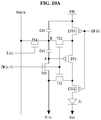
- FIGS. 10A and 10B show a pixel driving circuit and a gate signal waveform according to an aspect of the present disclosure
- FIGS. 11A and 11B show a pixel driving circuit and a gate signal waveform according to an aspect of the present disclosure
- FIGS. 12A and 12B show a pixel driving circuit and a gate signal waveform according to an aspect of the present disclosure.
- FIGS. 13A and 13B show a pixel driving circuit and a gate signal waveform according to an aspect of the present disclosure.
- temporal relationship for example, when a temporal relationship is described as “after,” “subsequently to,” “next,” “before,” and the like, a non-consecutive case may be included unless the term “immediately” or “directly” is used in the expression.
- a driving circuit and a gate driving circuit formed on a substrate of a display panel may be implemented as an N-type or P-type transistor.
- the transistor may be implemented as a transistor having a metal-oxide-semiconductor field-effect transistor (MOSFET) structure.
- MOSFET metal-oxide-semiconductor field-effect transistor
- the transistor is a three-electrode element including a gate, a source, and a drain.
- the source is an electrode for supplying carriers to the transistor. In the transistor, the carriers move from the source to the drain. In the case of an N-type transistor, the carriers are electrons. Thus, the electrons move from the source to the drain, and the source voltage is lower than the drain voltage.
- the direction of the current is from the drain to the source because the electrons move from the source to the drain.
- the carriers are holes.
- the source voltage is higher than the drain voltage so that the holes may move from the source to the drain.
- the direction of the current is from the source to the drain because the holes move from the source to the drain.
- the source and drain of the transistor are not fixed, and the source and drain of the transistor may be changed depending on an applied voltage.
- a gate-on voltage may be a voltage of a gate signal which may turn the transistor on.
- a gate-off voltage may be a voltage which may turn the transistor off.
- the turn-on voltage may be a gate low voltage, and the turn-off voltage may be a gate high voltage.
- the gate-on voltage may be a gate high voltage, and the gate-off voltage may be a gate low voltage.
- a driving circuit and an electroluminescent display device including the same according to an aspect of the present disclosure will be described below with reference to the accompanying drawings.
- FIG. 1 is a block diagram showing an electroluminescent display device according to an aspect of the present disclosure.
- an electroluminescent display device 100 includes a display panel 101 , a data driving circuit 102 which provides a signal to the display panel 101 , a gate driving circuit 108 , and a timing controller 110 .
- the display panel 101 may be divided into a display area DA where images are displayed and a non-display area NDA where no image is displayed.
- pixels for displaying an image are arranged.
- Each of the pixels may include a plurality of subpixels for implementing individual colors.
- the subpixels may be divided into red subpixels, green subpixels, and blue subpixels to implement the colors.
- one or more of the pixels may further include white subpixels.
- Each of the subpixels is connected to a data line arranged along a column line (or in a column direction) and is connected to a gate line arranged along a row line (or in a row direction). Subpixels disposed along the same row line share the same gate line and are driven at the same time. Also, when subpixels connected to a first gate line are defined as first subpixels and subpixels connected to an nth gate line are defined as nth subpixels, the first to nth subpixels are sequentially driven.
- Each of the subpixels includes a pixel driving circuit for emitting light of a light-emitting element EL, and the pixel driving circuit operates by receiving at least a data signal, a gate signal, and a power signal.
- the data signal is provided from a data driving circuit 102 to subpixels through a data line 4 a
- the gate signal is provided from a gate driving circuit 108 to subpixels through gate lines 2 a , 2 b , and 2 c
- the power signal is provided to subpixels through a power line 4 b .
- the power line 4 b may include a high-potential voltage line for supplying a high potential voltage to subpixels, a low-potential voltage electrode for supplying a low potential voltage to subpixels, and an initialization voltage line for supplying an initialization voltage to subpixels.
- the high-potential voltage is higher than the low-potential voltage and the initialization voltage, and the initialization voltage is lower than or equal to the low-potential voltage.
- the gate lines 2 a , 2 b , and 2 c may include multiple scan lines 2 a and 2 b through which a scan signal is supplied and multiple emission signal lines 2 c through which a light emission control signal is supplied.
- the data driving circuit 102 generates a data voltage by converting data of an input image received from the timing controller 110 into a gamma compensation voltage under the control of the timing controller 110 and outputs the generated data voltage to data lines 4 a .
- the data driving circuit 102 may be formed on the display panel 101 in the form of an integrated circuit (IC) or may be formed on the display panel 101 in the form of a chip-on-film (COF).
- the gate driving circuit 108 includes a scan driving circuit 103 and an emission driving circuit 104 .
- the scan driving circuit 103 sequentially supplies scan signals to the scan lines 2 a and 2 b under the control of the timing controller 110 .
- an nth scan signal applied to the nth gate line (here, n is a natural number) is synchronized with an nth data voltage.
- the emission driving circuit 104 generates an emission signal under the control of the timing controller 110 .
- the emission driving circuit 104 sequentially supplies emission signals to emission lines 2 c.
- the gate driving circuit 108 may be formed as an IC or may be formed as a gate in panel (GIP) embedded in the display panel 101 .
- the gate driving circuit 108 may be disposed on either or both of the left and right sides of the display panel 101 .
- the gate driving circuit 108 may be provided in the non-display area NDA.
- the timing controller 110 receives digital video data of the input image and a timing signal synchronized with the digital video data from a host system.
- the timing signal may include a data enable signal, a vertical synchronization signal, a horizontal synchronization signal, and a clock signal.
- the host system may be a television (TV) system, a set-top box, a navigation system, a digital video disc (DVD) player, a Blu-ray player, a personal computer, a home theater system, or a mobile information device.
- TV television
- DVD digital video disc
- Blu-ray player Blu-ray player
- the timing controller 110 generates a data timing control signal for controlling operation timing of the data driving circuit 102 , a gate timing control signal for controlling operation timing of the gate driving circuit 108 , etc. on the basis of the timing signal received from the host system.
- the gate timing control signal includes a start pulse, a shift clock, etc.
- the start pulse may define start timing at which a first output is generated for each shift register of the scan driving circuit 103 and the emission driving circuit 104 .
- the shift register starts to be driven when the start pulse is input and generates a first output signal at the first clock timing.
- the shift clock controls the output shift timing of the shift register.
- a period in which the subpixels present in the display area DA and arranged in the column direction are all driven may be referred to as a first frame period.
- the first frame period may be divided into a scan period in which data of the input image is addressed from gate lines connected to subpixels to the subpixels and then written in the subpixels and a emission period in which the subpixels repeatedly turn on and off according to an emission signal after the scan period.
- the scan period may be divided into a period for initializing driving circuits, a sampling period, and a programming period. The initialization of the driving circuits, the compensation for the threshold voltage of the driving transistor, and the charging of the data voltage are performed during the scan period, and the light emission operation is performed during the emission period. Since the scan period includes only several horizontal periods, most of one frame period is an emission period.
- a pixel driving circuit capable of accurately compensating for the threshold voltage of a driving transistor although the resolution and/or frequency of a display panel increases will be described below.
- FIGS. 2A and 2B show a pixel driving circuit and a gate signal waveform according to an aspect of the present disclosure.
- the pixel driving circuit shown in FIG. 2A will be described with regard to an nth subpixel disposed in an nth row of the display area DA.
- the pixel driving circuit for supplying a driving current to a light-emitting element EL includes a plurality of transistors and a plurality of capacitors.
- the pixel driving circuit according to an aspect of the present disclosure is an internal compensation circuit capable of compensating for the threshold voltage of a driving transistor DT 1 through the pixel driving circuit.
- Power supply voltages such as a high potential voltage Vdd, a low potential voltage Vss, and an initialization voltage Vini and pixel driving signals such as a first scan signal S 1 ( n ), a second scan signal S 2 ( n ), an emission signal EM(n), and a data voltage Vdata are applied to the pixel driving circuit.
- the scan signals S 1 ( n ) and S 2 ( n ) and the emission signal EM(n) have an on-level pulse or an off-level pulse at regular time intervals.
- the transistors according to an aspect of the present disclosure are implemented as p-type metal oxide semiconductor (PMOS) transistors.
- a transistor turn-on voltage is a gate low voltage (or an on-level pulse)
- a transistor turn-off voltage is a gate high voltage (an off-level pulse).
- the light-emitting element EL emits light by using the amount of current that is adjusted by the driving transistor DT 1 according to the data voltage Vdata, thereby representing brightness corresponding to the data gray-scale level of an input image.
- the light-emitting element EL may include an anode, a cathode, and an organic compound layer formed between the anode and the cathode.
- the organic compound layer may include a light-emitting layer, a hole injection layer, a hole transport layer, an electron transport layer, and an electron injection layer.
- the present disclosure is not limited thereto.
- the anode of the light-emitting element EL is connected to the driving transistor DT 1 , and the cathode of the light-emitting element EL is connected to a low potential voltage electrode to which the low potential voltage Vss is to be applied.
- the driving transistor DT 1 is a driving element configured to adjust electric current flowing through the light-emitting element EL according to a source-gate voltage Vsg.
- the driving transistor DT 1 includes a gate connected to a first node A, a source, and a drain.
- a first capacitor Cst includes two electrodes for forming first capacitance. One of the two electrodes is connected to the first node A, and the other is connected to a second node B.
- a second capacitor Cdt includes two electrodes for forming second capacitance. One of the two electrodes is connected to the second node B, and the other is connected to the high potential voltage line.
- a first switching circuit of the pixel driving circuit is turned on by the first scan signal S 1 ( n ) to initialize the gate of the driving transistor DT 1 and the anode of the light-emitting element EL and compensate for the threshold voltage of the driving transistor DT 1 .
- the first switching circuit includes three transistors, in particular an eleventh transistor T 11 , a twelfth transistor T 12 , and a thirteenth transistor T 13 .
- the eleventh transistor T 11 is turned on by the first scan signal S 1 ( n ) to provide the initialization voltage Vini to the first node A.
- the eleventh transistor T 11 is connected to the first node A and the initialization voltage line.
- the eleventh transistor T 11 may be implemented as a double-gate transistor. As shown in FIG. 2A , the double-gate transistor has two transistors T 11 a and T 11 b controlled by the same signal S 1 ( n ) and connected in series.
- the leakage current of the eleventh transistor T 11 may be reduced by implementing the eleventh transistor T 11 as a double-gate transistor because the eleventh transistor T 11 is connected to the first capacitor Cst.
- the leakage current of the eleventh transistor T 11 may be reduced by increasing a channel length of the transistor T 11 a , which is one of the two transistors and is more closely connected to the first node A, over a channel length of the transistor T 11 b , which is more closely connected to the initialization voltage line.
- the twelfth transistor T 12 is turned on by the first scan signal S 1 ( n ) to provide the initialization voltage Vini to the drain of the driving transistor DT 1 and the anode of the light-emitting element EL.
- the twelfth transistor T 12 is connected to the initialization voltage line, the drain of the driving transistor DT 1 , and the anode of the light-emitting element EL.
- the thirteenth transistor T 13 is turned on by the first scan signal S 1 ( n ) to provide the high potential voltage Vdd to the second node B.
- the thirteenth transistor T 13 is connected to the second node B and the source of the driving transistor DT 1 .
- the thirteenth transistor T 13 may indirectly receive the high potential voltage Vdd through another transistor.
- a second switching circuit of the pixel driving circuit may be turned on by a second scan signal S 2 ( n ) to apply the data voltage Vdata to the second node B.
- electric current corresponding to the data voltage Vdata may be generated from the driving transistor DT 1 .
- the second switching circuit includes a fourteenth transistor T 14 .
- the fourteenth transistor T 14 is turned on by the second scan signal S 2 ( n ) to provide the data voltage Vdata to the second node B.
- the fourteenth transistor T 14 is connected to the second node B and the data voltage line.
- the first scan signal S 1 ( n ) and the second scan signal S 2 ( n ) are provided to the first switching circuit and the second switching circuit through different scan driving circuits, respectively.
- a light emission control circuit of the pixel driving circuit according to an aspect of the present disclosure is turned on by the emission signal EM(n) to provide the high potential voltage Vdd to the driving transistor DT 1 .
- the driving transistor DT 1 is turned on to provide a driving current Ioled to the light-emitting element EL.
- the light emission control circuit includes an emission transistor ET 1 .
- the emission transistor ET 1 is turned on by the emission signal EM(n) to provide the high potential voltage Vdd to the driving transistor DT 1 .
- the emission transistor ET 1 is connected to the high potential voltage line and the source of the driving transistor DT 1 .
- the second scan signal S 2 ( n ) synchronized with the data voltage Vdata is supplied to the nth subpixel.
- the driving of the subpixel may be divided into an initialization period ⁇ circle around ( 1 ) ⁇ , a sampling period ⁇ circle around ( 2 ) ⁇ , a programming period ⁇ circle around ( 3 ) ⁇ , and a emission period ⁇ circle around ( 4 ) ⁇ .
- the initialization period ⁇ circle around ( 1 ) ⁇ and the programming period ⁇ circle around ( 3 ) ⁇ have one horizontal period 1H
- the sampling period ⁇ circle around ( 2 ) ⁇ has three horizontal periods 3H.
- the sampling period ⁇ circle around ( 2 ) ⁇ may be adjusted by the first scan signal S 1 ( n ).
- the first scan signal S 1 ( n ) is an on-level pulse during the initialization period ⁇ circle around ( 1 ) ⁇ and the sampling period ⁇ circle around ( 2 ) ⁇ and is an off-level pulse during the programming period ⁇ circle around ( 3 ) ⁇ and the emission period ⁇ circle around ( 4 ) ⁇ .
- the second scan signal S 2 ( n ) is an on-level pulse during the programming period ⁇ circle around ( 3 ) ⁇ and is an off-level pulse during the initialization period ⁇ circle around ( 1 ) ⁇ , the sampling period ⁇ circle around ( 2 ) ⁇ , and the emission period ⁇ circle around ( 4 ) ⁇ .
- the emission signal EM(n) is an on-level pulse during the initialization period ⁇ circle around ( 1 ) ⁇ and the emission period ⁇ circle around ( 4 ) ⁇ and is an off-level pulse during the sampling period ⁇ circle around ( 2 ) ⁇ and the programming period ⁇ circle around ( 3 ) ⁇ .
- the emission signal EM(n) is an off-level pulse during about four horizontal periods 4H in which the emission signal EM(n) overlaps the first scan signal S 1 ( n ) and the second scan signal S 2 ( n ).
- FIGS. 3A to 3D are diagrams illustrating operations for driving the pixel driving circuit shown in FIG. 2A . Each operation will be described in conjunction with FIG. 2B .
- FIG. 3A shows an operation of the pixel driving circuit during the initialization period ⁇ circle around ( 1 ) ⁇ .
- the first scan signal S 1 ( n ) switches from the off-level pulse to the on-level pulse.
- the emission signal EM(n) switches from the on-level pulse to the off-level pulse.
- the first switching circuits T 11 , T 12 , and T 13 , the driving transistor DT 1 , and the light emission control circuit ET 1 are turned on.
- the first node A and the initialization voltage line are electrically connected to each other, the anode and the initialization voltage line are electrically connected to each other, and the second node B and the high potential voltage line are electrically connected to each other.
- the gate of the driving transistor DT 1 is discharged with the initialization voltage Vini, and the high potential voltage Vdd is applied to the source of the driving transistor DT 1 .
- the gate-source voltage of the driving transistor DT 1 becomes lower than the threshold voltage of the driving transistor DT 1 . Accordingly, the driving transistor DT 1 is turned on.
- the initialization voltage Vini is lower than the low potential voltage Vss, no current flows to the light-emitting element EL, and thus the light-emitting element EL does not emit light.
- FIG. 3B shows an operation of the pixel driving circuit during the sampling period ⁇ circle around ( 2 ) ⁇ .
- the emission signal EM(n) switches to the off-level pulse
- the first scan signal S 1 ( n ) maintains the on-level pulse.
- the first switching circuits T 11 , T 12 , and T 13 and the driving transistor DT 1 remain turned on.
- the light emission control circuit ET 1 is turned off.
- the voltage of the second node B gradually decreases and converges to the sum of the initialization voltage Vini and the threshold voltage of the driving transistor DT 1 .
- the threshold voltage value of the driving transistor DT 1 is stored in the second node B.
- sufficient current should flow through turned-on transistors during the sampling period ⁇ circle around ( 2 ) ⁇ so that the driving transistor DT 1 can converge to an operating point state.
- the operating point state of the driving transistor DT 1 refers to a state in which the gate-source voltage of the driving transistor DT 1 is equal to the threshold voltage of the driving transistor DT 1 .
- the sampling period ⁇ circle around ( 2 ) ⁇ is set to three horizontal periods 3H.
- the present disclosure is not limited thereto.
- the sampling period ⁇ circle around ( 2 ) ⁇ may be secured to be greater than or equal to one horizontal period 1H.
- the data voltage Vdata is a signal that is provided to subpixels in one row during one horizontal period 1H.
- the sampling period ⁇ circle around ( 2 ) ⁇ can be set only to one horizontal period 1H or less. In this case, since the sampling period is not sufficiently secured, image quality defects may occur.
- the pixel driving circuit may sufficiently secure the sampling period ⁇ circle around ( 2 ) ⁇ to exceed one horizontal period 1H, and thus may accurately compensate for the threshold voltage of the driving transistor DT 1 . Also, even though the resolution and frequency of the display panel 101 increase, sufficient compensation time may be secured, and sampling time ⁇ circle around ( 2 ) ⁇ may be actively adjusted according to the resolution and frequency of the display panel 101 .
- FIG. 3C shows an operation of the pixel driving circuit during the programming period ⁇ circle around ( 3 ) ⁇ .
- the programming period ⁇ circle around ( 3 ) ⁇ starts, the first scan signal S 1 ( n ) switches from the on-level pulse to the off-level pulse, and the second scan signal S 2 ( n ) switches from the off-level pulse to the on-level pulse.
- the second switching circuit T 14 is turned on to electrically connect the data voltage line to the second node B.
- the first switching circuits T 11 , T 12 , and T 13 , the driving transistor DT 1 , and the light emission control circuit ET 1 are turned off.
- the data voltage Vdata is applied to the second node B, and the difference between the data voltage Vdata and the threshold voltage of the driving transistor DT 1 is applied to the first node A.
- the high potential voltage Vdd and the data voltage Vdata are applied to the two electrodes forming the second capacitor Cdt. Since the second capacitor Cdt is disposed between and connected to the first capacitor Cst and the high potential voltage line without directly connecting the first capacitor Cst to the high potential voltage line, the data voltage Vdata may be applied to the second node B.
- FIG. 3D shows an operation of the driving circuit during the emission period ⁇ circle around ( 4 ) ⁇ .
- the second scan signal S 2 ( n ) switches from the on-level pulse to the off-level pulse
- the emission signal EM(n) switches from the off-level pulse to the on-level pulse.
- the light emission control circuit ET 1 is turned on to electrically connect the high potential voltage Vdd to the source of the driving transistor DT 1
- the driving transistor DT 1 is turned on to provide the driving current Ioled to the light-emitting element EL.
- the driving current Ioled corresponds to Equation 1.
- I oled 1 2 ⁇ L W ⁇ C ox ⁇ ⁇ p ⁇ ( V dd - V data ) 2 [ Equation ⁇ ⁇ 1 ]
- L is the channel length of the driving transistor DT 1
- W is the channel width of the driving transistor DT 1
- Cox is parasitic capacitance between an active electrode and the gate of the driving transistor DT 1
- ⁇ p is mobility of the driving transistor DT 1 .
- the first capacitor Cst may constantly provide the driving current Ioled to the light-emitting element EL by maintaining a constant voltage applied to the gate of the driving transistor DT 1 during the emission period ⁇ circle around ( 4 ) ⁇ .
- FIG. 4 is a layout diagram of the pixel driving circuit shown in FIG. 2A
- FIG. 5 is a sectional view of a portion of FIG. 4 .
- a data line 14 a , a high potential voltage line 14 b , and an initialization voltage line 15 are arranged in the column direction, and a first scan line 12 a , a second scan line 12 b , and an emission line 12 c are arranged in the row direction.
- an active electrode 11 is connected to and formed integrally with where the channels of the transistors included in the first switching circuit, the second switching circuit, the driving transistor, and the light emission control circuit should be formed.
- the eleventh transistor T 11 and the twelfth transistor T 12 are disposed adjacent to each other, and one electrodes of the eleventh transistor T 11 and the twelfth transistor T 12 are connected to the initialization voltage line 15 through the same contact hole (a source contact hole CHs).
- the source contact hole CHs may overlap the initialization voltage line 15 so that the initialization voltage line 15 does not have to be branched.
- the initialization voltage line 15 is shown as being formed on a layer different from that of the data line 14 a and the high potential voltage line 14 b and as being formed of the same material as the anode electrode. However, the present disclosure is not limited thereto, and the initialization voltage line 15 may be formed on the same layer and of the same material as the data line 14 a and the high potential voltage line 14 b.
- the gate 12 of the driving transistor DT 1 is connected to the other electrode 14 d of the eleventh transistor T 11 through a gate contact hole CHg.
- the thirteenth electrode 13 of the first capacitor Cst forms a hole Hc to surround the gate contact hole CHg so that the other electrode 14 d of the eleventh transistor T 11 and the gate 12 of the driving transistor DT 1 are brought into contact with each other.
- the hole Hc formed by the thirteenth electrode 13 may not be short-circuited with the other electrode 14 d of the eleventh transistor T 11 and the gate 12 of the driving transistor DT 1 .
- the other electrode 14 d of the eleventh transistor T 11 may be formed on the same layer and of the same material as the data line 14 a and the high potential voltage line 14 b .
- the source of the driving transistor DT 1 is connected to the high potential voltage line 14 b through the light emission control circuit ET 1 .
- the drain of the driving transistor DT 1 is connected to the anode electrode 15 a through an anode contact hole CHa.
- the drain electrode connected to a drain area of the active electrode 11 of the driving transistor DT 1 is connected to the anode electrode 15 a through a connection electrode 14 c formed on the anode contact hole CHa.
- the initialization voltage line 15 is formed of the same material as the anode electrode, the anode electrode 15 a and the initialization voltage line 15 are formed on the same layer and spaced apart from each other.
- the initialization voltage line 15 may be formed to bypass the anode contact hole CHa so that the initialization voltage line 15 cannot be short-circuited with the anode contact hole CHa.
- the anode electrode 15 a does not overlap the initialization voltage line 15 and is formed separately for each subpixel.
- the connection electrode 14 c may be formed on the same layer and of the same material as the data line 14 a and the high potential voltage line 14 b.
- the first capacitor Cst includes a thirteenth electrode 13 and a twelfth electrode 12 , and the thirteenth electrode 13 serves as one electrode of the first capacitor Cst.
- the twelfth electrode 12 is located below the thirteenth electrode 13 , overlaps the thirteenth electrode 13 to form the first capacitance, and is the gate of the driving transistor DT 1 .
- the thirteenth electrode 13 is formed to be larger than the twelfth electrode 12 to overlap the twelfth electrode 12 .
- FIG. 5 is a sectional view of an area where the first capacitor Cst and the active electrode 11 overlap each other. However, the present disclosure is not limited thereto, and the area where the first capacitor Cst and the active electrode 11 do not overlap may be included in an area where the first capacitance is formed.
- the second capacitor Cdt includes a twenty-first electrode and a twenty-second electrode.
- the twenty-first electrode is a part where the thirteenth electrode 13 of the first capacitor Cst extends and overlaps the high potential voltage line 14 b
- the twenty-second electrode is a portion of the high potential voltage line 14 b overlapping the twenty-first electrode.
- the second capacitance is formed in an area where the twenty-first electrode and the twenty-second electrode overlap each other.
- the first capacitor Cst and the second capacitor Cdt share the same electrode 13 and form capacitance in different areas of the same electrode 13 while not overlapping each other.
- the first capacitor Cst has capacitance such that the voltage of the gate of the driving transistor DT 1 can remain constant.
- the capacitance of the first capacitor Cst is higher than the capacitance of the second capacitor Cdt in order to reduce the influence of kick-back and improve compensation performance. Since the capacitance is proportional to the area of the electrode of the capacitor, the area of the first capacitor Cst is greater than the area of the second capacitor Cdt.
- the area of the first capacitor Cst is more than twice as large as the area of the second capacitor Cdt.
- the area of the first capacitor Cst is less than twice as large as the area of the second capacitor Cdt.
- the area of the driving capacitor refers to an area where two electrodes forming capacitance overlap each other.
- the active electrode 11 , the twelfth electrode 12 of the first capacitor Cst, which is the gate electrode of the driving transistor DT 1 , the twenty-first electrode of the second capacitor Cdt, which is the thirteenth electrode 13 of the first capacitor Cst, and the high potential voltage line 14 b are sequentially stacked on a substrate 50 .
- Insulating layers 51 , 52 , 53 , and 54 are formed between the electrodes to insulate the electrodes in the entire area except for contact holes.
- the insulating layers 51 , 52 , and 53 may be mainly formed of a silicon-based inorganic material, and the insulating layer 54 covering a power supply line may be formed of a polyacrylic- or polyimide-based inorganic material.
- FIGS. 6A and 6B show a pixel driving circuit and a gate signal waveform according to an aspect of the present disclosure.
- the pixel driving circuit shown in FIG. 6A will be described with regard to the nth subpixel disposed in the nth row of the display area DA.
- the pixel driving circuit of FIG. 6A is a circuit that additionally includes a third switching circuit controlled by a second scan signal S 2 ( n ⁇ 4) applied to an (n ⁇ 4)th subpixel, and thus a description overlapping with the foregoing description with reference to FIG. 2A will be omitted or simplified.
- the pixel driving circuit according to an aspect of the present disclosure is an internal compensation circuit capable of compensating for the threshold voltage of a driving transistor DT 2 through the pixel driving circuit.
- Power supply voltages such as a high potential voltage Vdd, a low potential voltage Vss, and an initialization voltage Vini and pixel driving signals such as a first scan signal S 1 ( n ), a second scan signal S 2 ( n ), a second scan signal S 2 ( n ⁇ 4) applied to an (n ⁇ 4)th subpixel, an emission signal EM(n), and a data voltage Vdata are applied to the pixel driving circuit.
- the transistors according to an aspect of the present disclosure are implemented as PMOS transistors.
- the light-emitting element EL emits light by using the amount of current that is adjusted by the driving transistor DT 2 according to the data voltage Vdata, thereby representing brightness corresponding to the data gray level of an input image.
- the anode of the light-emitting element EL is connected to the driving transistor DT 2
- the cathode of the light-emitting element EL is connected to a low potential voltage electrode to which the low potential voltage Vss is to be applied.
- the driving transistor DT 2 is a driving element configured to adjust electric current flowing through the light-emitting element EL according to a gate-source voltage Vgs.
- the driving transistor DT 2 includes a gate connected to a first node A, a source, and a drain.
- a first capacitor Cst includes two electrodes for forming first capacitance. One of the two electrodes is connected to the first node A, and the other is connected to a second node B.
- a second capacitor Cdt includes two electrodes for forming second capacitance. One of the two electrodes is connected to the second node B, and the other is connected to the high potential voltage line.
- a first switching circuit of the pixel driving circuit is turned on by the first scan signal S 1 ( n ) to initialize the gate of the driving transistor DT 2 and the anode of the light-emitting element EL and compensate for the threshold voltage of the driving transistor DT 2 .
- the first switching circuit includes a twenty-first transistor T 21 , a twenty-second transistor T 22 , and a twenty-third transistor T 23 .
- the first switching circuit does not include a transistor for applying the data voltage Vdata to the pixel driving circuit.
- the twenty-first transistor T 21 is turned on by the first scan signal S 1 ( n ) to provide the initialization voltage Vini to the first node A.
- the twenty-first transistor T 21 is connected to the first node A and the initialization voltage line.
- the leakage current of the twenty-first transistor T 21 which is connected to the first capacitor Cst, may be reduced by implementing the twenty-first transistor T 21 as a double-gate transistor. Also, the leakage current of the twenty-first transistor T 21 may be reduced by increasing a channel length of one of the two transistors constituting the double-gate transistor, which is a transistor more closely connected to the first node A, more than a channel length of the other transistor, which is a transistor more closely connected to the initialization voltage line.
- the twenty-second transistor T 22 is turned on by the first scan signal S 1 ( n ) to provide the initialization voltage Vini to the anode of the light-emitting element EL.
- the twenty-second transistor T 22 is connected to the initialization voltage line and the anode of the light-emitting element EL.
- the twenty-third transistor T 23 is turned on by the first scan signal S 1 ( n ) to provide the high potential voltage Vdd to the second node B.
- the twenty-third transistor T 23 is connected to the second node B and the source of the driving transistor DT 2 .
- the twenty-third transistor T 23 may indirectly receive the high potential voltage Vdd through another transistor.
- a second switching circuit of the pixel driving circuit may be turned on by a second scan signal S 2 ( n ) to apply the data voltage Vdata to the second node B.
- electric current corresponding to the data voltage Vdata may be generated from the driving transistor DT 2 .
- the second switching circuit includes a twenty-fourth transistor T 24 .
- the twenty-fourth transistor T 24 is turned on by the second scan signal S 2 ( n ) to provide the data voltage Vdata to the second node B.
- the twenty-fourth transistor T 24 is connected to the second node B and the data voltage line.
- the first scan signal S 1 ( n ) and the second scan signal S 2 ( n ) are provided to the first switching circuit and the second switching circuit through different scan driving circuits, respectively.
- the pixel driving circuit is turned on by the second scan signal S 2 ( n ⁇ 4) applied to the (n ⁇ 4)th subpixel to apply the high potential voltage Vdd to the second node B by including a third switching circuit.
- the third switching circuit prevents the high potential voltage line from being short-circuited with the initialization voltage line and the low potential voltage electrode during the initialization period.
- the third switching circuit includes a twenty-fifth transistor T 25 .
- the twenty-fifth transistor T 25 is turned on by the second scan signal S 2 ( n ⁇ 4) applied to the (n ⁇ 4)th subpixel to provide the high potential voltage Vdd to the second node B.
- the twenty-fifth transistor T 25 is connected to the second node B and the high potential voltage line.
- a light emission control circuit of the pixel driving circuit according to an aspect of the present disclosure is turned on by the emission signal EM(n) to provide the high potential voltage Vdd to the driving transistor DT 2 .
- the driving transistor DT 2 is turned on to provide a driving current Ioled to the light-emitting element EL.
- the light emission control circuit includes an emission transistor ET 2 .
- the emission transistor ET 2 is turned on by the emission signal EM(n) to provide the high potential voltage Vdd to the driving transistor DT 2 .
- the emission transistor ET 2 is connected to the high potential voltage line and one electrode of the driving transistor DT 2 .
- the second scan signal S 2 ( n ⁇ 4) applied to the (n ⁇ 4)th subpixel is supplied to the nth subpixel.
- the second scan signal S 2 ( n ) synchronized with the data voltage Vdata is supplied to the nth subpixel.
- the driving of the subpixel may be divided into an initialization period ⁇ circle around ( 1 ) ⁇ , a sampling period ⁇ circle around ( 2 ) ⁇ , a programming period ⁇ circle around ( 3 ) ⁇ , and a emission period ⁇ circle around ( 4 ) ⁇ .
- the initialization period ⁇ circle around ( 1 ) ⁇ is one horizontal period 1H, and the emission signal EM(n) and the second scan signal S 2 ( n ⁇ 4) applied to the (n ⁇ 4)th subpixel are on-level pulses during the initialization period ⁇ circle around ( 1 ) ⁇ .
- the twenty-fifth transistor T 25 is turned on by the second scan signal S 2 ( n ⁇ 4) applied to the (n ⁇ 4)th subpixel to apply the high potential voltage Vdd to the second node B.
- the emission transistor ET 2 is turned on by the emission signal EM(n) to apply the high potential voltage Vdd to the source of the driving transistor DT 2 .
- the source of the driving transistor DT 2 and the second node B are set to the high potential voltage Vdd.
- the sampling period ⁇ circle around ( 2 ) ⁇ is shown as having three horizontal periods 3H. However, the present disclosure is not limited thereto.
- the sampling period ⁇ circle around ( 2 ) ⁇ may be adjusted by the first scan signal S 1 ( n ). During the sampling period ⁇ circle around ( 2 ) ⁇ , the first scan signal S 1 ( n ) is an on-level pulse and the emission signal EM(n) is an off-level pulse.
- the first switching circuits T 21 , T 22 , and T 23 which have been turned on, discharge the gate of the driving transistor DT 2 and the anode of the light-emitting element EL with the initialization voltage and turn on the driving transistor DT 2 to sense the threshold voltage of the driving transistor DT 2 .
- the sampling period ⁇ circle around ( 2 ) ⁇ is set to three horizontal periods 3H.
- the present disclosure is not limited thereto.
- the sampling period ⁇ circle around ( 2 ) ⁇ may be secured to be greater than or equal to one horizontal period 1H.
- the pixel driving circuit may sufficiently secure the sampling period ⁇ circle around ( 2 ) ⁇ to exceed one horizontal period 1H and thus may accurately compensate for the threshold voltage of the driving transistor DT 2 . Also, even though the resolution and frequency of the display panel 101 increase, sufficient compensation time may be secured, and sampling time ⁇ circle around ( 2 ) ⁇ may be adjusted according to the resolution and frequency of the display panel 101 .
- the programming period ⁇ circle around ( 3 ) ⁇ is one horizontal period 1H
- the second scan signal S 2 ( n ) is an on-level pulse during the programming period ⁇ circle around ( 3 ) ⁇ .
- the first switching circuits T 21 , T 22 , and T 23 , the driving transistor DT 2 , and the light emission control circuit ET 2 are turned off.
- the twenty-fourth transistor T 24 is turned on by the second scan signal S 2 ( n ) to apply the data voltage Vdata to the second node B, and the difference between the threshold voltage of the driving transistor DT 2 and the data voltage Vdata is applied to the first node A due to the coupling effect of the first capacitor Cst.
- the high potential voltage Vdd and the data voltage Vdata are applied to the two electrodes forming the second capacitor Cdt. Since the second capacitor Cdt is disposed between and connected to the first capacitor Cst and the high potential voltage line without directly connecting the first capacitor Cst to the high potential voltage line, the data voltage Vdata may be applied to the second node B.
- the emission signal EM(n) is an on-level pulse
- the second scan signal S 2 ( n ) is an off-level pulse.
- the emission signal EM(n) maintains an off-level pulse during about four horizontal periods 4H in which the emission signal EM(n) overlaps the first scan signal S 1 ( n ) and the second scan signal S 2 ( n ).
- the light emission control circuit ET 2 is turned on to electrically connect the high potential voltage Vdd to the source of the driving transistor DT 2 , and the driving transistor DT 2 is turned on to provide the driving current Ioled to the light-emitting element EL.
- the driving current Ioled corresponds to Equation 1. Referring to Equation 1, since the threshold voltage value of the driving transistor is removed from the driving current Ioled, the driving current Ioled does not depend on the threshold voltage of the driving transistor and is not affected even by the change of the threshold voltage.
- the first capacitor Cst may constantly provide the driving current Ioled to the light-emitting element EL by maintaining a constant voltage applied to the gate of the driving transistor DT 2 during the emission period ⁇ circle around ( 4 ) ⁇ .
- FIGS. 7A and 7B show a pixel driving circuit and a gate signal waveform according to an aspect of the present disclosure.
- the driving circuit shown in FIG. 7A will be described with regard to the nth subpixel disposed in the nth row of the display area DA.
- the driving circuit of FIG. 7A is a circuit in which an emission transistor ET 32 is added to the driving circuit of FIG. 2A , and thus a description overlapping with the foregoing description with reference to FIG. 2A will be omitted or simplified.
- the driving circuit according to an aspect of the present disclosure is an internal compensation circuit capable of compensating for the threshold voltage of a driving transistor DT 3 through the driving circuit.
- Power supply voltages such as a high potential voltage Vdd, a low potential voltage Vss, and an initialization voltage Vini and pixel driving signals such as a first scan signal S 1 ( n ), a second scan signal S 2 ( n ), an emission signal EM(n), and a data voltage Vdata are applied to the driving circuit.
- the transistors according to an aspect of the present disclosure are implemented as PMOS transistors.
- the light-emitting element EL emits light by using the amount of current that is adjusted by the driving transistor DT 3 according to the data voltage Vdata, thereby representing brightness corresponding to the data gray level of an input image.
- the anode of the light-emitting element EL is connected to the light emission control circuit, and the cathode of the light-emitting element EL is connected to a low potential voltage electrode to which the low potential voltage Vss is to be applied.
- the driving transistor DT 3 is a driving element configured to adjust electric current flowing through the light-emitting element EL according to a gate-source voltage Vgs.
- the driving transistor DT 3 includes a gate connected to a first node A, a source, and a drain.
- a first capacitor Cst includes two electrodes for forming first capacitance. One of the two electrodes is connected to the first node A, and the other is connected to a second node B.
- a second capacitor Cdt includes two electrodes for forming second capacitance. One of the two electrodes is connected to the second node B, and the other is connected to the high potential voltage line.
- a first switching circuit of the pixel driving circuit is turned on by the first scan signal S 1 ( n ) to initialize the gate and drain of the driving transistor DT 3 and compensate for the threshold voltage of the driving transistor DT 3 .
- the first switching circuit includes a thirty-first transistor T 31 , a thirty-second transistor T 32 , and a thirty-third transistor T 33 .
- the first switching circuit does not include a transistor for applying the data voltage Vdata to the pixel driving circuit.
- the thirty-first transistor T 31 is turned on by the first scan signal S 1 ( n ) to provide the initialization voltage Vini to the first node A.
- the thirty-first transistor T 31 is connected to the first node A and the initialization voltage line.
- the leakage current of the thirty-first transistor T 31 which is connected to the first capacitor Cst, may be reduced by implementing the thirty-first transistor T 31 as a double-gate transistor. Also, the leakage current of the thirty-first transistor T 31 may be reduced by increasing a channel length of one of the two transistors constituting the double-gate transistor, which is a transistor more closely connected to the first node A, more than a channel length of the other transistor, which is a transistor more closely connected to the initialization voltage line.
- the thirty-second transistor T 32 is turned on by the first scan signal S 1 ( n ) to provide the initialization voltage Vini to the drain of the driving transistor DT 3 .
- the thirty-second transistor T 32 is connected to the initialization voltage line and the drain of the driving transistor DT 3 .
- the thirty-third transistor T 33 is turned on by the first scan signal S 1 ( n ) to provide the high potential voltage Vdd to the second node B.
- the thirty-third transistor T 33 is connected to the second node B and the source of the driving transistor DT 3 .
- the thirty-third transistor T 33 may indirectly receive the high potential voltage Vdd through another transistor.
- a second switching circuit of the driving circuit according to an aspect of the present disclosure may be turned on by a second scan signal S 2 ( n ) to apply the data voltage Vdata to the second node B.
- electric current corresponding to the data voltage Vdata may be generated from the driving transistor DT 3 .
- the second switching circuit includes a thirty-fourth transistor T 34 .
- the thirty-fourth transistor T 34 is turned on by the second scan signal S 2 ( n ) to provide the data voltage Vdata to the second node B.
- the thirty-fourth transistor T 34 is connected to the second node B and the data voltage line.
- the first scan signal S 1 ( n ) and the second scan signal S 2 ( n ) are provided to the first switching circuit and the second switching circuit through different scan driving circuits, respectively.
- a light emission control circuit of the driving circuit according to an aspect of the present disclosure is turned on by the emission signal EM(n) to provide the high potential voltage Vdd to the driving transistor DT 2 .
- the driving transistor DT 3 is turned on to generate the driving current Ioled and form a current path between the driving transistor DT 3 and the light-emitting element EL.
- the light emission control circuit includes a first emission transistor ET 31 and a second emission transistor ET 32 .
- the first emission transistor ET 31 is turned on by the emission signal EM(n) to provide the high potential voltage Vdd to the driving transistor DT 3 .
- the first emission transistor ET 31 is connected to the high potential voltage line and the source of the driving transistor DT 3 .
- the second emission transistor ET 32 is turned on by the emission signal EM(n) to provide the driving current generated by the driving transistor DT 3 to the anode of the light-emitting element EL.
- the second emission transistor ET 32 is additionally included, resistance increases compared to a structure with only the first emission transistor ET 31 .
- current that may flow to the light-emitting element EL during the initialization period may be further decreased. Therefore, since the black screen becomes darker, it is possible to improve the contrast ratio of the display panel.
- the anode of the light-emitting element EL is discharged with the initialization voltage during the initialization period.
- the second scan signal S 2 ( n ) synchronized with the data voltage Vdata is supplied to the nth subpixel.
- the driving of the subpixel may be divided into an initialization period ⁇ circle around ( 1 ) ⁇ , a sampling period ⁇ circle around ( 2 ) ⁇ , a programming period ⁇ circle around ( 3 ) ⁇ , and a emission period ⁇ circle around ( 4 ) ⁇ .
- the initialization period is one horizontal period 1H, and the first scan signal S 1 ( n ) and the emission signal EM(n) are on-level pulses during the initialization period ⁇ circle around ( 1 ) ⁇ . Therefore, the first switching circuits T 31 , T 32 , and T 33 , the driving transistor DT 3 , and the light emission control circuits ET 31 and ET 32 are turned on. As a result, the first node A and the initialization voltage line are electrically connected to each other, the anode and the initialization voltage line are electrically connected to each other, and the second node B and the high potential voltage line are electrically connected to each other.
- the first scan signal S 1 ( n ) is an on-level pulse
- the emission signal EM(n) is an off-level pulse.
- the first switching circuits T 31 , T 32 , and T 33 and the driving transistor DT 3 which are turned on during the sampling period ⁇ circle around ( 2 ) ⁇ , sense the threshold voltage of the driving transistor DT 3 .
- the sampling period ⁇ circle around ( 2 ) ⁇ is set to three horizontal periods 3H.
- the present disclosure is not limited thereto.
- the sampling period ⁇ circle around ( 2 ) ⁇ may be secured to be greater than or equal to one horizontal period 1H.
- the pixel driving circuit may sufficiently secure the sampling period ⁇ circle around ( 2 ) ⁇ to exceed one horizontal period 1H and thus may accurately compensate for the threshold voltage of the driving transistor DT 3 . Also, even though the resolution and frequency of the display panel 101 increase, sufficient compensation time may be secured, and sampling time ⁇ circle around ( 2 ) ⁇ may be adjusted according to the resolution and frequency of the display panel 101 .
- the second switching circuit T 34 is turned on to electrically connect the data voltage line to the second node B.
- the first switching circuits T 31 , T 32 , and T 33 , the driving transistor DT 3 , and the light emission control circuits ET 31 and ET 32 are turned off.
- the data voltage Vdata is applied to the second node B
- the difference between the data voltage Vdata and the threshold voltage of the driving transistor DT 3 is applied to the first node A due to the coupling effect of the first capacitor Cst.
- the high potential voltage Vdd and the data voltage Vdata are applied to the two electrodes forming the second capacitor Cdt. Since the second capacitor Cdt is disposed between and connected to the first capacitor Cst and the high potential voltage line without directly connecting the first capacitor Cst to the high potential voltage line, the data voltage Vdata may be applied to the second node B.
- the light emission control circuits ET 31 and ET 32 are turned on to electrically connect the high potential voltage Vdd to the source of the driving transistor DT 3 , and the driving transistor DT 3 is turned on to provide the driving current Ioled to the light-emitting element EL.
- the driving current Ioled corresponds to Equation 1. Referring to Equation 1, since the threshold voltage value of the driving transistor is removed from the driving current Ioled, the driving current Ioled does not depend on the threshold voltage of the driving transistor and is not affected even by the change of the threshold voltage.
- the first capacitor Cst may constantly provide the driving current Ioled to the light-emitting element EL by maintaining a constant voltage applied to the gate of the driving transistor DT 3 during the emission period ⁇ circle around ( 4 ) ⁇ .
- FIG. 8 is a layout diagram of the pixel driving circuit shown in FIG. 7A .
- a data line 24 a , a high potential voltage line 24 b , and an initialization voltage line 24 c are arranged in the column direction, and a first scan line 22 a , a second scan line 22 b , and an emission line 22 c are arranged in the row direction.
- an active electrode 21 is connected to and formed integrally with where channels of transistors included in a first switching circuit, a second switching circuit, a driving transistor, and a light emission control circuit should be formed.
- the thirty-first transistor T 31 and the thirty-second transistor T 32 are disposed adjacent to each other, and one electrodes of the thirty-first transistor T 31 and the thirty-second transistor T 32 are connected to the initialization voltage line 24 c through the same contact hole (a source contact hole CHs).
- the source contact hole CHs may overlap the initialization voltage line 24 c such that the initialization voltage line 24 c does not have to be branched.
- the initialization voltage line 24 c is formed on the same layer and of the same material as the data line 24 a and the high potential voltage line 24 b.
- the source of the driving transistor DT 3 is connected to the high potential voltage line 24 b through the first emission transistor ET 31 , and the drain of the driving transistor DT 3 is connected to the anode electrode through an anode contact hole CHa.
- the gate 22 of the driving transistor DT 3 is connected to the other electrode 24 d of the thirty-first transistor T 31 through a gate contact hole CHg.
- the twenty-third electrode 23 of the first capacitor Cst forms a hole Hc to surround the gate contact hole CHg so that the other electrode 24 d of the thirty-first transistor T 31 and the gate 22 of the driving transistor DT 3 are brought into contact with each other.
- the hole Hc formed by the twenty-third electrode 23 may not be short-circuited with the other electrode 24 d of the thirty-first transistor T 31 and the gate 22 of the driving transistor DT 3 .
- the first capacitor Cst includes a twenty-third electrode 23 and a twenty-second electrode 22 , and the twenty-third electrode 23 serves as one electrode of the first capacitor Cst.
- the twenty-second electrode 22 is located below the twenty-third electrode 23 , overlaps the twenty-third electrode 23 to form the first capacitance, and serves as the gate of the driving transistor DT 3 .
- the twenty-third electrode 23 is formed to be larger than the twenty-second electrode 22 to overlap the twenty-second electrode 22 .
- the second capacitor Cdt includes a twenty-fifth electrode and a twenty-sixth electrode.
- the twenty-fifth electrode is a part where the twenty-third electrode 23 of the first capacitor Cst extends and overlaps the high potential voltage line 24 b
- the twenty-sixth electrode is a portion of the high potential voltage line 24 b overlapping the twenty-fifth electrode.
- the second capacitance is formed in an area where the twenty-fifth electrode and the twenty-sixth electrode overlap each other.
- the area of the twenty-sixth electrode may be expanded by protruding a portion of the high potential voltage line 24 b .
- the first capacitor Cst and the second capacitor Cdt share the same electrode 23 and form capacitance in different areas of the same electrode 23 while not overlapping each other.
- FIGS. 9A and 9B show a pixel driving circuit and a gate signal waveform according to an aspect of the present disclosure.
- the pixel driving circuit shown in FIG. 9A will be described with regard to the nth subpixel disposed in the nth row of the display area DA.
- the driving circuit of FIG. 9A is a circuit including all of the elements of FIGS. 6A and 7A , and thus a description overlapping with the foregoing description with reference to FIGS. 6A and 7A will be omitted or simplified.
- the pixel driving circuit according to an aspect of the present disclosure is an internal compensation circuit capable of compensating for the threshold voltage of a driving transistor DT 4 through the pixel driving circuit.
- Power supply voltages such as a high potential voltage Vdd, a low potential voltage Vss, and an initialization voltage Vini and pixel driving signals such as a first scan signal S 1 ( n ), a second scan signal S 2 ( n ), a second scan signal S 2 ( n ⁇ 4) applied to an (n ⁇ 4) th subpixel, an emission signal EM(n), and a data voltage Vdata are applied to the driving circuit.
- the transistors according to an aspect of the present disclosure are implemented as PMOS transistors.
- the light-emitting element EL emits light by using the amount of current that is adjusted by the driving transistor DT 4 according to the data voltage Vdata, thereby representing brightness corresponding to the data gray level of an input image.
- the anode of the light-emitting element EL is connected to the light emission control circuit, and the cathode of the light-emitting element EL is connected to a low potential voltage electrode to which the low potential voltage Vss is to be applied.
- the driving transistor DT 4 is a driving element configured to adjust electric current flowing through the light-emitting element EL according to a gate-source voltage Vgs.
- the driving transistor DT 4 includes a gate connected to a first node A, a source, and a drain.
- a first capacitor Cst includes two electrodes for forming first capacitance. One of the two electrodes is connected to the first node A, and the other is connected to a second node B.
- a second capacitor Cdt includes two electrodes for forming second capacitance. One of the two electrodes is connected to the second node B, and the other is connected to the high potential voltage line.
- a first switching circuit of the pixel driving circuit is turned on by the first scan signal S 1 ( n ) to initialize the gate and drain of the driving transistor DT 4 and compensate for the threshold voltage of the driving transistor DT 4 .
- the first switching circuit includes a forty-first transistor T 41 , a forty-second transistor T 42 , and a forty-third transistor T 43 .
- the data voltage Vdata is not used to compensate for the threshold voltage of the driving transistor DT 4 , and thus the first switching circuit does not include a transistor for applying the data voltage Vdata to the pixel driving circuit.
- the forty-first transistor T 41 is turned on by the first scan signal S 1 ( n ) to provide the initialization voltage Vini to the first node A.
- the forty-first transistor T 41 is connected to the first node A and the initialization voltage line.
- the leakage current of the forty-first transistor T 41 which is connected to the first capacitor Cst, may be reduced by implementing the forty-first transistor T 41 as a double-gate transistor. Also, the leakage current of the forty-first transistor T 41 may be reduced by increasing a channel length of one of the two transistors constituting the double-gate transistor, which is more closely connected to the first node A, more than a channel length of the other transistor, which is more closely connected to the initialization voltage line.
- the forty-second transistor T 42 is turned on by the first scan signal S 1 ( n ) to provide the initialization voltage Vini to the drain of the driving transistor DT 4 .
- the forty-second transistor T 42 is connected to the initialization voltage line and the drain of the driving transistor DT 4 .
- the forty-third transistor T 43 is turned on by the first scan signal S 1 ( n ) to provide the high potential voltage Vdd to the second node B.
- the forty-third transistor T 43 is connected to the second node B and one electrode of the driving transistor DT 4 .
- the forty-third transistor T 43 may indirectly receive the high potential voltage Vdd through another transistor.
- a second switching circuit of the pixel driving circuit may be turned on by a second scan signal S 2 ( n ) to apply the data voltage Vdata to the second node B.
- electric current corresponding to the data voltage Vdata may be generated from the driving transistor DT 4 .
- the second switching circuit includes a forty-fourth transistor T 44 .
- the forty-fourth transistor T 44 is turned on by the second scan signal S 2 ( n ) to provide the data voltage Vdata to the second node B.
- the forty-fourth transistor T 44 is connected to the second node B and the data voltage line.
- the first scan signal S 1 ( n ) and the second scan signal S 2 ( n ) are provided to the first switching circuit and the second switching circuit through different scan driving circuits, respectively.
- the driving circuit according to an aspect of the present disclosure is turned on by the second scan signal S 2 ( n ⁇ 4) applied to the (n ⁇ 4)th subpixel to apply the high potential voltage Vdd to the second node B by including a third switching circuit.
- the third switching circuit prevents the high potential voltage line from being short-circuited with the initialization voltage line and the low potential voltage electrode during the initialization period.
- the third switching circuit includes a forty-fifth transistor T 45 .
- the forty-fifth transistor T 45 is turned on by the second scan signal S 2 ( n ⁇ 4) applied to the (n ⁇ 4)th subpixel to provide the high potential voltage Vdd to the second node B.
- the forty-fifth transistor T 45 is connected to the second node B and the high potential voltage line.
- a light emission control circuit of the driving circuit according to an aspect of the present disclosure is turned on by the emission signal EM(n) to provide the high potential voltage Vdd to the driving transistor DT 4 .
- the driving transistor DT 4 is turned on to generate the driving current Ioled and form a current path between the driving transistor DT 4 and the light-emitting element EL.
- the light emission control circuit includes a first emission transistor ET 41 and a second emission transistor ET 42 .
- the first emission transistor ET 41 is turned on by the emission signal EM(n) to provide the high potential voltage Vdd to the driving transistor DT 4 .
- the first emission transistor ET 41 is connected to the high potential voltage line and the source of the driving transistor DT 4 .
- the second emission transistor ET 42 is turned on by the emission signal EM(n) to provide the driving current generated by the driving transistor DT 4 to the anode of the light-emitting element EL.
- the second emission transistor ET 42 is additionally included, resistance increases compared to a structure with only the first emission transistor ET 41 .
- current that may flow to the light-emitting element EL during the initialization period may be further decreased. Therefore, since the black screen becomes darker, it is possible to improve the contrast ratio of the display panel.
- the anode of the light-emitting element EL is discharged with the initialization voltage during the initialization period.
- the second scan signal S 2 ( n ⁇ 4) applied to the (n ⁇ 4)th subpixel is supplied to the nth subpixel.
- the second scan signal S 2 ( n ) synchronized with the data voltage Vdata is supplied to the nth subpixel.
- the driving of the subpixel may be divided into an initialization period ⁇ circle around ( 1 ) ⁇ , a sampling period ⁇ circle around ( 2 ) ⁇ , a programming period ⁇ circle around ( 3 ) ⁇ , and an emission period ⁇ circle around ( 4 ) ⁇ .
- the initialization period ⁇ circle around ( 1 ) ⁇ is one horizontal period 1H, and the emission signal EM(n) and the second scan signal S 2 ( n ⁇ 4) applied to the (n ⁇ 4)th subpixel are on-level pulses during the initialization period ⁇ circle around ( 1 ) ⁇ .
- the forty-fifth transistor T 45 is turned on by the second scan signal S 2 ( n ⁇ 4) applied to the (n ⁇ 4)th subpixel to apply the high potential voltage Vdd to the second node B.
- the first emission transistor ET 41 is turned on by the emission signal EM(n) to apply the high potential voltage Vdd to the source of the driving transistor DT 4 .
- the source of the driving transistor DT 4 and the second node B are set to the high potential voltage Vdd.
- the sampling period ⁇ circle around ( 2 ) ⁇ is shown as having three horizontal periods 3H. However, the present disclosure is not limited thereto.
- the sampling period ⁇ circle around ( 2 ) ⁇ may be adjusted by the first scan signal S 1 ( n ). During the sampling period ⁇ circle around ( 2 ) ⁇ , the first scan signal S 1 ( n ) remains as an on-level pulse, and the emission signal EM(n) switches to an off-level pulse.
- the first switching circuits T 41 , T 42 , and T 43 which have been turned on, discharge the gate and drain of the driving transistor DT 4 by using the initialization voltage Vini and turn on the driving transistor DT 4 to sense the threshold voltage of the driving transistor DT 4 .
- the initialization voltage Vini is applied to the first node A
- the sum of the initialization voltage Vini and the threshold voltage of the driving transistor DT 4 is applied to the second node B. Accordingly, the threshold voltage value of the driving transistor DT 4 is stored in the second node B.
- the sampling period ⁇ circle around ( 2 ) ⁇ is set to three horizontal periods 3H.
- the present disclosure is not limited thereto.
- the sampling period ⁇ circle around ( 2 ) ⁇ may be secured to be greater than or equal to one horizontal period 1H.
- the pixel driving circuit may sufficiently secure the sampling period ⁇ circle around ( 2 ) ⁇ to exceed one horizontal period 1H and thus may accurately compensate for the threshold voltage of the driving transistor DT 4 . Also, even though the resolution and frequency of the display panel 101 increase, sufficient compensation time may be secured, and sampling time ⁇ circle around ( 2 ) ⁇ may be adjusted according to the resolution and frequency of the display panel 101 .
- the programming period ⁇ circle around ( 3 ) ⁇ is one horizontal period 1H
- the second scan signal S 2 ( n ) is an on-level pulse during the programming period ⁇ circle around ( 3 ) ⁇ .
- the first switching circuits T 41 , T 42 , and T 43 , the driving transistor DT 4 , and the light emission control circuits ET 41 and ET 42 are turned off.
- the forty-fourth transistor T 44 is turned on by the second scan signal S 2 ( n ) to apply the data voltage Vdata to the second node B, and the difference between the threshold voltage of the driving transistor DT 4 and the data voltage Vdata is applied to the first node A due to the coupling effect of the first capacitor Cst.
- the high potential voltage Vdd and the data voltage Vdata are applied to the two electrodes forming the second capacitor Cdt. Since the second capacitor Cdt is disposed between and connected to the first capacitor Cst and the high potential voltage line without directly connecting the first capacitor Cst to the high potential voltage line, the data voltage Vdata may be applied to the second node B.
- the emission signal EM(n) is an on-level pulse
- the second scan signal S 2 ( n ) is an off-level pulse.
- the emission signal EM(n) maintains an off-level pulse during about four horizontal periods 4H in which the emission signal EM(n) overlaps the first scan signal S 1 ( n ) and the second scan signal S 2 ( n ).
- the light emission control circuits ET 41 and ET 42 are turned on to electrically connect the high potential voltage Vdd to the source of the driving transistor DT 4 , and the driving transistor DT 4 is turned on to provide the driving current Ioled to the light-emitting element EL.
- the driving current Ioled corresponds to Equation 1. Referring to Equation 1, since the threshold voltage value of the driving transistor is removed from the driving current Ioled, the driving current Ioled does not depend on the threshold voltage of the driving transistor and is not affected even by the change of the threshold voltage.
- the first capacitor Cst may constantly provide the driving current Ioled to the light-emitting element EL by maintaining a constant voltage applied to the gate of the driving transistor DT 4 during the emission period ⁇ circle around ( 4 ) ⁇ .
- FIGS. 10A and 10B show a pixel driving circuit and a gate signal waveform according to an aspect of the present disclosure.
- the pixel driving circuit shown in FIG. 10A will be described with regard to the nth subpixel disposed in the nth row of the display area DA.
- the driving circuit of FIG. 10A is a circuit in which some transistors included in the pixel driving circuit of FIG. 7A are implemented as n-type metal oxide semiconductor (NMOS) transistors, and thus a description overlapping with the foregoing description with reference to FIG. 7A will be omitted or simplified.
- NMOS n-type metal oxide semiconductor
- the pixel driving circuit according to an aspect of the present disclosure is an internal compensation circuit capable of compensating for the threshold voltage of a driving transistor DT 5 through the pixel driving circuit.
- Power supply voltages such as a high potential voltage Vdd, a low potential voltage Vss, and an initialization voltage Vini and pixel driving signals such as a scan signal S(n), an emission signal applied to an (n ⁇ 1)th subpixel, an emission signal EM(n), and a data voltage Vdata are applied to the pixel driving circuit.
- the transistors according to an aspect of the present disclosure are implemented as NMOS transistors and PMOS transistors.
- the turn-on voltage of the NMOS transistor is a gate high voltage
- the turn-off voltage of the NMOS transistor is a gate low voltage
- the turn-on voltage of the PMOS transistor is a gate low voltage
- the turn-off voltage of the PMOS transistor is a gate high voltage.
- the light-emitting element EL emits light by using the amount of current that is adjusted by the driving transistor DT 5 according to the data voltage Vdata, thereby representing brightness corresponding to the data gray level of an input image.
- the anode of the light-emitting element EL is connected to the light emission control circuit, and the cathode of the light-emitting element EL is connected to a low potential voltage electrode to which the low potential voltage Vss is to be applied.
- the driving transistor DT 5 is a driving element configured to adjust electric current flowing through the light-emitting element EL according to a gate-source voltage Vgs.
- the driving transistor DT 5 is implemented as a PMOS transistor and includes a gate connected to a first node A, a source, and a drain.
- a first capacitor Cst includes two electrodes for forming first capacitance. One of the two electrodes is connected to the first node A, and the other is connected to a second node B.
- a second capacitor Cdt includes two electrodes for forming second capacitance. One of the two electrodes is connected to the second node B, and the other is connected to the high potential voltage line.
- a first switching circuit of the pixel driving circuit is turned on by the emission signal EM(n ⁇ 1) applied to the (n ⁇ 1)th subpixel to initialize the gate and drain of the driving transistor DT 5 and compensate for the threshold voltage of the driving transistor DT 5 .
- the first switching circuit includes a fifty-first transistor T 51 , a fifty-second transistor T 52 , and a fifty-third transistor T 53 which are implemented as NMOS transistors.
- the first switching circuit does not include a transistor for applying the data voltage Vdata to the pixel driving circuit.
- the fifty-first transistor T 51 is turned on by the emission signal EM(n ⁇ 1) applied to the (n ⁇ 1)th subpixel to provide the initialization voltage Vini to the first node A.
- the fifty-first transistor T 51 is connected to the first node A and the initialization voltage line.
- the leakage current of the fifty-first transistor T 51 which is connected to the first capacitor Cst, may be reduced by implementing the fifty-first transistor T 51 as a double-gate transistor. Also, the leakage current of the fifty-first transistor T 51 may be reduced by increasing a channel length of one of the two transistors constituting the double-gate transistor, which is more closely connected to the first node A, more than a channel length of the other transistor, which is more closely connected to the initialization voltage line.
- the fifty-second transistor T 52 is turned on by the emission signal EM(n ⁇ 1) applied to the (n ⁇ 1)th subpixel to provide the initialization voltage Vini to the drain of the driving transistor DT 5 .
- the fifty-second transistor T 52 is connected to the initialization voltage line and the drain of the driving transistor DT 5 .
- the fifty-third transistor T 53 is turned on by the emission signal EM(n ⁇ 1) applied to the (n ⁇ 1)th subpixel to provide the high potential voltage Vdd to the second node B.
- the fifty-third transistor T 53 is connected to the second node B and the source of the driving transistor DT 5 .
- the fifty-third transistor T 53 may indirectly receive the high potential voltage Vdd through another transistor.
- a second switching circuit of the pixel driving circuit may be turned on by the scan signal S(n) to apply the data voltage Vdata to the second node B.
- electric current corresponding to the data voltage Vdata may be generated from the driving transistor DT 5 .
- the second switching circuit includes a fifty-fourth transistor T 54 which is implemented as an NMOS transistor.
- the fifty-fourth transistor T 54 is turned on by the scan signal S(n) to provide the data voltage Vdata to the second node B.
- the fifty-fourth transistor T 54 is connected to the second node B and the data voltage line.
- a light emission control circuit of the pixel driving circuit is turned on by the emission signal EM(n) to provide the high potential voltage Vdd to the driving transistor DT 5 .
- the driving transistor DT 5 is turned on to generate the driving current Ioled and form a current path between the driving transistor DT 5 and the light-emitting element EL.
- the light emission control circuit includes a first emission transistor ET 51 and a second emission transistor ET 52 which are implemented as PMOS transistors.
- the first emission transistor ET 51 is turned on by the emission signal EM(n) to provide the high potential voltage Vdd to the driving transistor DT 5 .
- the first emission transistor ET 51 is connected to the high potential voltage line and the source of the driving transistor DT 5 .
- the second emission transistor ET 52 is turned on by the emission signal EM(n) to provide the driving current generated by the driving transistor DT 5 to the anode of the light-emitting element EL.
- the second emission transistor ET 52 is additionally included, resistance increases compared to a structure with only the first emission transistor ET 51 .
- current that may flow to the light-emitting element EL during the initialization period may be further decreased. Therefore, since the black screen becomes darker, it is possible to improve the contrast ratio of the display panel.
- the anode of the light-emitting element EL is discharged with the initialization voltage during the initialization period.
- FIG. 11B is a waveform chart of a gate signal of the driving circuit of FIG. 11A . Even when the second emission transistor ET 52 is omitted, the driving circuit may operate with the same gate signal waveform as that shown in FIG. 10B .
- the scan signal S 2 ( n ) synchronized with the data voltage Vdata is supplied to the nth subpixel.
- the driving of the subpixel may be divided into an initialization period ⁇ circle around ( 1 ) ⁇ , a sampling period ⁇ circle around ( 2 ) ⁇ , a programming period ⁇ circle around ( 3 ) ⁇ , and a emission period ⁇ circle around ( 4 ) ⁇ .
- the initialization period ⁇ circle around ( 1 ) ⁇ and the programming period ⁇ circle around ( 3 ) ⁇ have one horizontal period 1H, and the sampling period ⁇ circle around ( 2 ) ⁇ has three horizontal periods 3H.
- the sampling period ⁇ circle around ( 2 ) ⁇ may be controlled by the emission signal EM(n ⁇ 1) applied to the (n ⁇ 1)th subpixel such that the horizontal periods are adjusted.
- the emission signal EM(n ⁇ 1) applied to the (n ⁇ 1)th subpixel is an on-level pulse during the initialization period ⁇ circle around ( 1 ) ⁇ and the sampling period ⁇ circle around ( 2 ) ⁇ and is an off-level pulse during the programming period ⁇ circle around ( 3 ) ⁇ and the emission period ⁇ circle around ( 4 ) ⁇ .
- the scan signal S(n) is an on-level pulse during the programming period ⁇ circle around ( 3 ) ⁇ and is an off-level pulse during the initialization period ⁇ circle around ( 1 ) ⁇ , the sampling period ⁇ circle around ( 2 ) ⁇ , and the emission period ⁇ circle around ( 4 ) ⁇ .
- the emission signal EM(n) is an on-level pulse during the initialization period ⁇ circle around ( 1 ) ⁇ and the emission period ⁇ circle around ( 4 ) ⁇ and is an off-level pulse during the sampling period ⁇ circle around ( 2 ) ⁇ and the programming period ⁇ circle around ( 3 ) ⁇ .
- the emission signal EM(n) maintains an off-level pulse during about four horizontal periods 4H in which the emission signal EM(n) overlaps the scan signal S(n) and the emission signal EM(n ⁇ 1) applied to the (n ⁇ 1)th subpixel.
- the on-level pulse of the emission signal EM(n ⁇ 1) applied to the (n ⁇ 1)th subpixel, which is applied to the first switching circuit is a gate high voltage
- the off-level pulse of the emission signal EM(n ⁇ 1) is a gate low voltage
- the on-level pulse of the scan signal S(n), which is applied to the second switching circuit is a gate high voltage
- the off-level pulse of the scan signal S(n) is a gate low voltage
- the on-level pulse of the emission signal EM(n), which is applied to the light emission control circuit is a gate low voltage
- the off-level pulse of the emission signal EM(n) is a gate high voltage.
- the first switching circuits T 51 , T 52 , and T 53 , the driving transistor DT 5 , and the light emission control circuits ET 51 and ET 52 are turned on during the initialization period ⁇ circle around ( 1 ) ⁇ .
- the first node A and the initialization voltage line are electrically connected to each other
- the anode and the initialization voltage line are electrically connected to each other
- the second node B and the high potential voltage line are electrically connected to each other.
- the first switching circuits T 51 , T 52 , and T 53 and the driving transistor DT 5 are turned on. Also, the light emission control circuits ET 51 and ET 52 are turned off. Thus, the voltage of the second node B gradually decreases and converges to the sum of the initialization voltage Vini and the threshold voltage of the driving transistor DT 5 . Accordingly, the threshold voltage value of the driving transistor DT 5 is stored in the second node B.
- the sampling period ⁇ circle around ( 2 ) ⁇ is set to three horizontal periods 3H.
- the present disclosure is not limited thereto.
- the sampling period ⁇ circle around ( 2 ) ⁇ may be secured to be greater than or equal to one horizontal period 1H.
- the pixel driving circuit may sufficiently secure the sampling period ⁇ circle around ( 2 ) ⁇ to exceed one horizontal period 1H and thus may accurately compensate for the threshold voltage of the driving transistor DT 5 . Also, even though the resolution and frequency of the display panel 101 increase, sufficient compensation time may be secured, and sampling time ⁇ circle around ( 2 ) ⁇ may be adjusted according to the resolution and frequency of the display panel 101 .
- the second switching circuit T 54 is turned on to electrically connect the data voltage line to the second node B.
- the first switching circuits T 51 , T 52 , and T 53 , the driving transistor DT 5 , and the light emission control circuits ET 51 and ET 52 are turned off.
- the data voltage Vdata is applied to the second node B, and the difference between the data voltage Vdata and the threshold voltage of the driving transistor DT 5 is applied to the first node A due to the coupling effect of the first capacitor Cst.
- the high potential voltage Vdd and the data voltage Vdata are applied to the two electrodes forming the second capacitor Cdt. Since the second capacitor Cdt is disposed between and connected to the first capacitor Cst and the high potential voltage line without directly connecting the first capacitor Cst to the high potential voltage line, the data voltage Vdata may be applied to the second node B.
- the light emission control circuits ET 51 and ET 52 are turned on to electrically connect the high potential voltage Vdd to the source of the driving transistor DT 5 , and the driving transistor DT 5 is turned on to provide the driving current Ioled to the light-emitting element EL.
- the driving current Ioled corresponds to Equation 1. Referring to Equation 1, since the threshold voltage value of the driving transistor is removed from the driving current Ioled, the driving current Ioled does not depend on the threshold voltage of the driving transistor and is not affected even by the change of the threshold voltage.
- the first capacitor Cst may constantly provide the driving current Ioled to the light-emitting element EL by maintaining a constant voltage applied to the gate of the driving transistor DT 5 during the emission period ⁇ circle around ( 4 ) ⁇ .
- FIGS. 12A and 12B show a pixel driving circuit and a gate signal waveform according to an aspect of the present disclosure.
- the pixel driving circuit shown in FIG. 12A will be described with regard to the nth subpixel disposed in the nth row of the display area DA.
- the pixel driving circuit of FIG. 12A is a circuit in which some transistors included in the pixel driving circuit of FIG. 9A are implemented as NMOS transistors, and thus a description overlapping with the foregoing description with reference to FIG. 9A will be omitted or simplified.
- the pixel driving circuit according to an aspect of the present disclosure is an internal compensation circuit capable of compensating for the threshold voltage of a driving transistor DT 7 through the pixel driving circuit.
- Power supply voltages such as a high potential voltage Vdd, a low potential voltage Vss, and an initialization voltage Vini
- pixel driving signals such as a scan signal S(n), a scan signal S(n ⁇ 4) applied to an (n ⁇ 1)th subpixel, an emission signal EM(n), and a data voltage Vdata, are applied to the pixel driving circuit.
- the scan signals S(n) and S(n ⁇ 4) and the emission signal EM(n) have a gate low voltage or a gate high voltage at regular time intervals.
- the transistors according to an aspect of the present disclosure are implemented as NMOS transistors and PMOS transistors.
- the light-emitting element EL emits light by using the amount of current that is adjusted by the driving transistor DT 7 according to the data voltage Vdata, thereby representing brightness corresponding to the data gray level of an input image.
- the anode of the light-emitting element EL is connected to the light emission control circuit, and the cathode of the light-emitting element EL is connected to a low potential voltage electrode to which the low potential voltage Vss is to be applied.
- the driving transistor DT 7 is a driving element configured to adjust electric current flowing through the light-emitting element EL according to a gate-source voltage Vgs.
- the driving transistor DT 5 is implemented as a PMOS transistor and includes a gate connected to a first node A, a source, and a drain.
- a first capacitor Cst includes two electrodes for forming first capacitance. One of the two electrodes is connected to the first node A, and the other is connected to a second node B.
- a second capacitor Cdt includes two electrodes for forming second capacitance. One of the two electrodes is connected to the second node B, and the other is connected to the high potential voltage line.
- a first switching circuit of the pixel driving circuit is turned on by the emission signal EM(n) to initialize the gate and drain of the driving transistor DT 7 and compensate for the threshold voltage of the driving transistor DT 7 .
- the first switching circuit includes a seventy-first transistor T 71 , a seventy-second transistor T 72 , and a seventy-third transistor T 73 which are implemented as NMOS transistors.
- the first switching circuit does not include a transistor for applying the data voltage Vdata to the pixel driving circuit.
- the seventy-first transistor T 71 is turned on by the emission signal EM(n) to provide the initialization voltage Vini to the first node A.
- the seventy-first transistor T 71 is connected to the first node A and the initialization voltage line.
- the leakage current of the seventy-first transistor T 71 which is connected to the first capacitor Cst, may be reduced by implementing the seventy-first transistor T 71 as a double-gate transistor.
- the leakage current of the seventy-first transistor T 71 may be reduced by increasing a channel length of one of the two transistors constituting the double-gate transistor, which is more closely connected to the first node A, more than a channel length of the other transistor, which is more closely connected to the initialization voltage line.
- the seventy-second transistor T 72 is turned on by the emission signal EM(n) to provide the initialization voltage Vini to the anode of the light-emitting element EL.
- the seventy-second transistor T 72 is connected to the initialization voltage line and the drain of the driving transistor DT 7 .
- the seventy-third transistor T 73 is turned on by the emission signal EM(n) to provide the high potential voltage Vdd to the second node B.
- the seventy-third transistor T 73 is connected to the second node B and the source of the driving transistor DT 7 .
- the seventy-third transistor T 73 may indirectly receive the high potential voltage Vdd through another transistor.
- a second switching circuit of the pixel driving circuit may be turned on by the scan signal S(n) to apply the data voltage Vdata to the second node B.
- electric current corresponding to the data voltage Vdata may be generated from the driving transistor DT 7 .
- the second switching circuit includes a seventy-fourth transistor T 74 which is implemented as an NMOS transistor.
- the seventy-fourth transistor T 74 is turned on by the scan signal S(n) to provide the data voltage Vdata to the second node B.
- the seventy-fourth transistor T 74 is connected to the second node B and the data voltage line.
- the pixel driving circuit is turned on by the scan signal S(n ⁇ 4) applied to the (n ⁇ 4)th subpixel to apply the high potential voltage Vdd to the second node B.
- the third switching circuit prevents the high potential voltage line from being short-circuited with the initialization voltage line and the low potential voltage electrode during the initialization period.
- the third switching circuit includes a seventy-fifth transistor T 75 which is implemented as an NMOS transistor.
- the seventy-fifth transistor T 75 is turned on by the scan signal S(n ⁇ 4) applied to the (n ⁇ 4)th subpixel to provide the high potential voltage Vdd to the second node B.
- the seventy-fifth transistor T 75 is connected to the second node B and the high potential voltage line.
- a light emission control circuit of the pixel driving circuit according to an aspect of the present disclosure is turned on by the emission signal EM(n) to provide the high potential voltage Vdd to the driving transistor DT 7 .
- the driving transistor DT 7 is turned on to generate the driving current Ioled and form a current path between the driving transistor DT 7 and the light-emitting element EL.
- the light emission control circuit includes a first emission transistor ET 71 and a second emission transistor ET 72 which are implemented as PMOS transistors.
- the first emission transistor ET 71 is turned on by the emission signal EM(n) to provide the high potential voltage Vdd to the driving transistor DT 7 .
- the emission transistor ET 71 is connected to the high potential voltage line and the source of the driving transistor DT 7 .
- the second emission transistor ET 72 is turned on by the emission signal EM(n) to provide the driving current generated by the driving transistor DT 7 to the anode of the light-emitting element EL.
- the second emission transistor ET 72 is additionally included, resistance increases compared to a structure with only the first emission transistor ET 71 .
- current that may flow to the light-emitting element EL during the initialization period may be further decreased. Therefore, since the black screen becomes darker, it is possible to improve the contrast ratio of the display panel.
- the anode of the light-emitting element EL is discharged with the initialization voltage during the initialization period.
- FIG. 13B is a waveform chart of a gate signal of the driving circuit of FIG. 13A . Even when the second emission transistor ET 72 is omitted, the driving circuit may operate with the same gate signal waveform as that shown in FIG. 12B .
- the driving of the subpixel may be divided into an initialization period ⁇ circle around ( 1 ) ⁇ , a sampling period ⁇ circle around ( 2 ) ⁇ , a programming period ⁇ circle around ( 3 ) ⁇ , and a emission period ⁇ circle around ( 4 ) ⁇ .
- the initialization period ⁇ circle around ( 1 ) ⁇ and the programming period ⁇ circle around ( 3 ) ⁇ have one horizontal period 1H, and the sampling period ⁇ circle around ( 2 ) ⁇ has three horizontal periods 3H.
- the sampling period ⁇ circle around ( 2 ) ⁇ may be controlled by the emission signal EM(n) such that the horizontal periods are adjusted.
- the scan signal S(n ⁇ 4) applied to the (n ⁇ 4)th subpixel remains as an on-level pulse during the initialization period ⁇ circle around ( 1 ) ⁇ and remains as an off-level pulse during the other periods.
- the emission signal EM(n) remains as a gate high voltage during the sampling period ⁇ circle around ( 2 ) ⁇ and remains as a gate low voltage during the other periods.
- the scan signal S(n) remains as an on-level pulse during the programming period ⁇ circle around ( 3 ) ⁇ and remains as the off-level pulse during the other periods.
- the gate high voltage of the emission signal EM(n) is an on-level pulse when the gate high voltage is applied to the first switching circuit and is an off-level pulse when the gate high voltage is applied to the light emission control circuit.
- the on-level pulse of the scan signal S(n), which is applied to the second switching circuit, is a gate high voltage
- the off-level pulse of the scan signal S(n) is a gate low voltage.
- the on-level pulse of the scan signal S(n ⁇ 4), which is applied to the (n ⁇ 4)th subpixel, is a gate high voltage
- the off-level pulse of the scan signal S(n ⁇ 4) is a gate low voltage.
- the third switching circuit is turned on. Since the emission signal EM(n) is a gate low voltage, the light emission control circuit is turned on.
- the seventy-fifth transistor T 75 is turned on by the scan signal S(n ⁇ 4) applied to the (n ⁇ 4)th subpixel to apply the high potential voltage Vdd to the second node B.
- the emission transistors ET 71 and ET 72 are turned on by the emission signal EM(n) to apply the high potential voltage Vdd to the source of the driving transistor DT 7 .
- the source of the driving transistor DT 7 and the second node B are set to the high potential voltage Vdd.
- the circuit controlled by the emission signal EM(n) includes the first switching circuit and the light emission control circuit. Since the first switching circuit is implemented using NMOS transistors and the light emission control circuit is implemented using PMOS transistors, the light emission control circuit is turned off when the first switching circuit is turned on, and is turned on when the first switching circuit is turned off. Accordingly, the first switching circuit and the light emission control circuit may be controlled through one gate driving circuit, and thus the size of the gate driving circuit may be reduced.
- the sampling period ⁇ circle around ( 2 ) ⁇ is shown as having three horizontal periods 3H. However, the present disclosure is not limited thereto.
- the sampling period ⁇ circle around ( 2 ) ⁇ may be adjusted by the emission signal EM(n), and the gate high voltage is maintained during the sampling period ⁇ circle around ( 2 ) ⁇ .
- the first switching circuits T 71 , T 72 , and T 73 which have been turned on, discharge the gate and drain of the driving transistor DT 7 by using the initialization voltage Vini and turn on the driving transistor DT 7 to sense the threshold voltage of the driving transistor DT 7 .
- the initialization voltage Vini is applied to the first node A, and the sum of the initialization voltage Vini and the threshold voltage of the driving transistor DT 7 is applied to the second node B. Accordingly, the threshold voltage value of the driving transistor DT 7 is stored in the second node B.
- the sampling period ⁇ circle around ( 2 ) ⁇ is set to three horizontal periods 3H.
- the present disclosure is not limited thereto.
- the sampling period ⁇ circle around ( 2 ) ⁇ may be secured to be greater than or equal to one horizontal period 1H.
- the pixel driving circuit may sufficiently secure the sampling period ⁇ circle around ( 2 ) ⁇ to exceed one horizontal period 1H and thus may accurately compensate for the threshold voltage of the driving transistor DT 7 . Also, even though the resolution and frequency of the display panel 101 increase, sufficient compensation time may be secured, and sampling time ⁇ circle around ( 2 ) ⁇ may be adjusted according to the resolution and frequency of the display panel 101 .
- the programming period ⁇ circle around ( 3 ) ⁇ is one horizontal period 1H
- the second scan signal S 2 ( n ) is an on-level pulse during the programming period ⁇ circle around ( 3 ) ⁇ .
- the first switching circuits T 71 , T 72 , and T 73 , the driving transistor DT 7 , and the light emission control circuits ET 71 and ET 72 are turned off.
- the seventy-fourth transistor T 74 is turned on by the scan signal S(n) to apply the data voltage Vdata to the second node B, and the difference between the threshold voltage of the driving transistor DT 7 and the data voltage Vdata is applied to the first node A due to the coupling effect of the first capacitor Cst.
- the high potential voltage Vdd and the data voltage Vdata are applied to the two electrodes forming the second capacitor Cdt. Since the second capacitor Cdt is disposed between and connected to the first capacitor Cst and the high potential voltage line without directly connecting the first capacitor Cst to the high potential voltage line, the data voltage Vdata may be applied to the second node B.
- the emission signal EM(n) maintains a gate low voltage.
- the light emission control circuits ET 71 and ET 72 are turned on to electrically connect the high potential voltage Vdd to the source of the driving transistor DT 7 , and the driving transistor DT 7 is turned on to provide the driving current Ioled to the light-emitting element EL.
- the driving current Ioled corresponds to Equation 1. Referring to Equation 1, since the threshold voltage value of the driving transistor is removed from the driving current Ioled, the driving current Ioled does not depend on the threshold voltage of the driving transistor and is not affected even by the change of the threshold voltage.
- the first capacitor Cst may constantly provide the driving current Ioled to the light-emitting element EL by maintaining a constant voltage applied to the gate of the driving transistor DT 7 during the emission period ⁇ circle around ( 4 ) ⁇ .
- An electroluminescent display panel including the pixel driving circuit according to an aspect of the present disclosure will be described as follows.
- each of a plurality of subpixels included in an nth row includes a pixel driving circuit that is driven according to an initialization period, a sampling period, a programming period, and an emission period
- the pixel driving circuit comprises a light-emitting element, a first capacitor connected to a first node and a second node, a second capacitor connected to the second node and a high potential voltage line which provides a high potential voltage, a driving transistor configured to supply electric current to the light-emitting element and controlled by a voltage applied to the first node, a first switching circuit controlled by a first scan signal and turned on during the sampling period to compensate for a time-varying characteristic of the driving transistor, a second switching circuit controlled by a second scan signal and turned on during the programming period to apply a data voltage to the second node, and a light emission control circuit controlled by an emission signal and turned on during the initialization period and the emission period
- the sampling period is longer as one horizontal period or has a period exceeding the one horizontal period, and the initialization period and the programming period are equal to one horizontal period.
- a sampling period can be provided for a high-resolution/high-frequency display panel which is sufficiently long, since usually in common high-resolution/high-frequency display panels the horizontal period is decreased.
- the sampling period may be sufficiently secured, and thus it is possible to improve an image quality of the display panel by enhancing compensation capability of a pixel driving circuit.
- the first scan signal and the second scan signal may be output from different scan driving circuits.
- the area of the first capacitor may be twice as large as the area of the second capacitor.
- the first switching circuit may be turned on during the initialization period, a gate of the driving transistor may be discharged with an initialization voltage, and the high potential voltage may be applied to the second node.
- the pixel driving circuit may further include a third switching circuit connected to the high potential voltage line and the second node, and the third switching circuit may be controlled by the second scan signal provided in an (n ⁇ 4)th row and may be turned on during the initialization period.
- the first switching circuit may include a first transistor connected to the first node and an initialization voltage line, a second transistor connected to the initialization voltage line and a drain of the driving transistor, and a third transistor connected to the second node and a source of the driving transistor.
- the first transistor may comprise two transistors implemented as a double-gate transistor, and one of the two transistors which is connected to the first node may have a greater channel length than the other transistor which is connected to the initialization voltage line.
- the light emission control circuit may include a first emission transistor connected to the high potential voltage line and a source of the driving transistor and turned on by the emission signal and a second emission transistor connected to a drain of the driving transistor and an anode of the light-emitting element and turned on by the emission signal.
- the sampling period may vary depending on a resolution of the electroluminescent display panel.
- each of a plurality of subpixels included in an nth row includes a pixel driving circuit that is driven according to an initialization period, a sampling period, a programming period, and an emission period
- the pixel driving circuit includes a light-emitting element, a first capacitor connected to a first node and a second node, a second capacitor connected to the second node and a high potential voltage line, a driving transistor configured to supply electric current to the light-emitting element and controlled by a voltage applied to the first node, a first switching circuit controlled by a first emission signal and turned on during the sampling period to compensate for a time-varying characteristic of the driving transistor, a second switching circuit controlled by a scan signal and turned on during the programming period to apply a data voltage to the second node, and a light emission control circuit controlled by a second emission signal and turned on during the initialization period and the emission period to apply the high potential voltage
- the sampling period is longer as one horizontal period or has a period exceeding one horizontal period, and the initialization period and the programming period are equal to the one horizontal period.
- a sampling period can be provided for a high-resolution/high-frequency display panel which is sufficiently long, since usually in common high-resolution/high-frequency display panels the horizontal period is decreased.
- the sampling period may be sufficiently secured, and thus it is possible to improve an image quality of the display panel by enhancing compensation capability of a pixel driving circuit.
- the area of the first capacitor may be twice as large as the area of the second capacitor.
- the first switching circuit may be an NMOS transistor, and the light emission control circuit may be a PMOS transistor.
- the first emission signal is an emission signal provided in an (n ⁇ 1) th row.
- the first switch circuit may be turned on even during the initialization period, the gate of the driving transistor may be discharged with the initialization voltage, and the high potential voltage may be applied to the second node.
- the first emission signal and the second emission signal are the same emission signal provided in an (n) th row.
- the pixel driving circuit may further include a third switching circuit connected to the high potential voltage line which provides the high potential voltage and the second node. Also, the third switching circuit may be turned on during the initialization period, and the turn-on and turn-off of the third switching circuit may be controlled by a second scan signal provided in an (n ⁇ 4) th row.
- the first switching circuit may include a first transistor connected to the first node and an initialization voltage line, a second transistor connected to the initialization voltage line and a drain of the driving transistor, and a third transistor connected to the second node and a source of the driving transistor.
- the light emission control circuit may include a first emission transistor connected to the high potential voltage line and a source of the driving transistor and turned on by the emission signal and a second emission transistor connected to a drain of the driving transistor and an anode of the light-emitting element and turned on by the emission signal.
- the sampling period it is possible to secure the sampling period to be greater than or equal to one horizontal period by implementing the pixel driving circuit such that the data voltage is not used to compensate for the threshold voltage of the driving transistor.
- the high potential voltage line is short-circuited with the initialization voltage line and the low potential voltage electrode during the initialization period by including a third switching circuit so that the third switching circuit is turned on by the second scan signal applied to subpixels in rows prior to the nth row to apply the high potential voltage to a node to which the data voltage is to be applied.
Landscapes
- Engineering & Computer Science (AREA)
- Physics & Mathematics (AREA)
- Computer Hardware Design (AREA)
- General Physics & Mathematics (AREA)
- Theoretical Computer Science (AREA)
- Microelectronics & Electronic Packaging (AREA)
- Control Of Indicators Other Than Cathode Ray Tubes (AREA)
- Control Of El Displays (AREA)
- Electroluminescent Light Sources (AREA)
Applications Claiming Priority (2)
| Application Number | Priority Date | Filing Date | Title |
|---|---|---|---|
| KR10-2019-0144624 | 2019-11-12 | ||
| KR1020190144624A KR20210057629A (ko) | 2019-11-12 | 2019-11-12 | 화소 구동 회로를 포함한 전계발광 표시패널 |
Publications (1)
| Publication Number | Publication Date |
|---|---|
| US10964264B1 true US10964264B1 (en) | 2021-03-30 |
Family
ID=73149559
Family Applications (1)
| Application Number | Title | Priority Date | Filing Date |
|---|---|---|---|
| US15/930,344 Active US10964264B1 (en) | 2019-11-12 | 2020-05-12 | Electroluminescent display panel having pixel driving circuit |
Country Status (7)
| Country | Link |
|---|---|
| US (1) | US10964264B1 (ja) |
| JP (1) | JP7165707B2 (ja) |
| KR (1) | KR20210057629A (ja) |
| CN (1) | CN112863435B (ja) |
| DE (1) | DE102020116090A1 (ja) |
| GB (1) | GB2589713B (ja) |
| TW (1) | TWI739520B (ja) |
Cited By (14)
| Publication number | Priority date | Publication date | Assignee | Title |
|---|---|---|---|---|
| CN113112960A (zh) * | 2021-04-08 | 2021-07-13 | 京东方科技集团股份有限公司 | 一种像素电路及其驱动方法、显示装置 |
| US20210327341A1 (en) * | 2020-04-21 | 2021-10-21 | Samsung Display Co., Ltd. | Display device |
| CN113628585A (zh) * | 2021-08-31 | 2021-11-09 | 上海视涯技术有限公司 | 像素驱动电路及其驱动方法、硅基显示面板和显示装置 |
| CN113808542A (zh) * | 2021-09-22 | 2021-12-17 | 北京京东方技术开发有限公司 | 像素电路、驱动方法和显示装置 |
| CN113870758A (zh) * | 2021-09-18 | 2021-12-31 | 云谷(固安)科技有限公司 | 像素电路及其驱动方法、显示面板 |
| US11217177B2 (en) * | 2019-12-16 | 2022-01-04 | Samsung Display Co., Ltd. | Emission driver and display device including the same |
| US20220084472A1 (en) * | 2020-09-11 | 2022-03-17 | Samsung Display Co., Ltd. | Pixel of an organic light emitting diode display device, and organic light emitting diode display device |
| US11373597B2 (en) * | 2020-02-24 | 2022-06-28 | Samsung Display Co., Ltd. | Organic light emitting diode display device and method of driving the same |
| US11410604B2 (en) * | 2020-03-31 | 2022-08-09 | Chengdu Boe Optoelectronics Technology Co., Ltd. | Pixel circuit and a method of driving the same and a display panel |
| US20220270552A1 (en) * | 2018-10-08 | 2022-08-25 | Samsung Display Co., Ltd. | Display device |
| US20220284860A1 (en) * | 2021-03-04 | 2022-09-08 | Apple Inc. | Displays with Reduced Temperature Luminance Sensitivity |
| US20220343842A1 (en) * | 2020-05-26 | 2022-10-27 | Boe Technology Group Co., Ltd. | Pixel driving circuit, method for driving the same and display device |
| US20230112488A1 (en) * | 2021-09-30 | 2023-04-13 | Samsung Display Co., Ltd. | Pixel and display device including the same |
| US20230317004A1 (en) * | 2022-03-30 | 2023-10-05 | Samsung Display Co., Ltd. | Emissive display device |
Families Citing this family (4)
| Publication number | Priority date | Publication date | Assignee | Title |
|---|---|---|---|---|
| TWI828189B (zh) * | 2021-07-08 | 2024-01-01 | 南韓商Lg顯示器股份有限公司 | 像素電路及包含該像素電路的顯示裝置 |
| CN113870786B (zh) * | 2021-09-28 | 2023-01-10 | 京东方科技集团股份有限公司 | 像素电路、驱动发光和显示装置 |
| KR20230139824A (ko) | 2022-03-22 | 2023-10-06 | 삼성디스플레이 주식회사 | 표시 장치 및 이의 구동 방법 |
| CN114627804B (zh) * | 2022-03-28 | 2023-08-01 | 武汉华星光电技术有限公司 | 像素电路及显示面板 |
Citations (2)
| Publication number | Priority date | Publication date | Assignee | Title |
|---|---|---|---|---|
| US20140184665A1 (en) * | 2012-12-28 | 2014-07-03 | Lg Display Co., Ltd. | Organic light emitting diode display device and method for driving the same |
| US20170154572A1 (en) * | 2015-12-01 | 2017-06-01 | Lg Display Co., Ltd. | Organic light emitting diode display |
Family Cites Families (18)
| Publication number | Priority date | Publication date | Assignee | Title |
|---|---|---|---|---|
| KR101080351B1 (ko) | 2004-06-22 | 2011-11-04 | 삼성전자주식회사 | 표시 장치 및 그 구동 방법 |
| JP2010122320A (ja) | 2008-11-17 | 2010-06-03 | Toshiba Mobile Display Co Ltd | アクティブマトリクス型表示装置 |
| KR101199106B1 (ko) | 2010-03-17 | 2012-11-09 | 삼성디스플레이 주식회사 | 유기전계발광 표시장치 |
| KR20140013707A (ko) * | 2012-07-26 | 2014-02-05 | 삼성디스플레이 주식회사 | 화소 및 이를 이용한 유기전계발광 표시장치 |
| KR20140081262A (ko) | 2012-12-21 | 2014-07-01 | 삼성디스플레이 주식회사 | 화소 및 이를 이용한 유기전계발광 표시장치 |
| CN104167167A (zh) * | 2013-05-17 | 2014-11-26 | 友达光电股份有限公司 | 像素电路及其驱动方法、显示装置 |
| KR102244816B1 (ko) * | 2014-08-25 | 2021-04-28 | 삼성디스플레이 주식회사 | 화소 및 이를 포함하는 유기 발광 표시 장치용 기판 |
| CN104200771B (zh) * | 2014-09-12 | 2017-03-01 | 上海天马有机发光显示技术有限公司 | 像素电路、阵列基板及显示装置 |
| TWI544266B (zh) * | 2015-06-03 | 2016-08-01 | 友達光電股份有限公司 | 畫素電路 |
| KR102294133B1 (ko) * | 2015-06-15 | 2021-08-27 | 삼성디스플레이 주식회사 | 유기발광 디스플레이 장치의 스캔 드라이버, 유기발광 디스플레이 장치 및 이를 포함하는 디스플레이 시스템 |
| CN104916257A (zh) * | 2015-07-15 | 2015-09-16 | 京东方科技集团股份有限公司 | 一种像素电路及其驱动方法、显示面板和显示装置 |
| CN105139807B (zh) | 2015-10-22 | 2019-01-04 | 京东方科技集团股份有限公司 | 一种像素驱动电路、显示装置及其驱动方法 |
| CN105427800B (zh) * | 2016-01-06 | 2018-06-12 | 京东方科技集团股份有限公司 | 像素电路、驱动方法、有机电致发光显示面板及显示装置 |
| CN106023900A (zh) * | 2016-08-01 | 2016-10-12 | 上海天马有机发光显示技术有限公司 | 一种有机发光显示面板及其驱动方法 |
| CN106409233B (zh) * | 2016-11-28 | 2019-08-06 | 上海天马有机发光显示技术有限公司 | 一种像素电路、其驱动方法及有机发光显示面板 |
| US10127859B2 (en) * | 2016-12-29 | 2018-11-13 | Lg Display Co., Ltd. | Electroluminescent display |
| WO2019014935A1 (en) * | 2017-07-21 | 2019-01-24 | Huawei Technologies Co., Ltd. | ADVANCED PIXEL CIRCUIT FOR DISPLAY |
| TWI639149B (zh) * | 2018-03-09 | 2018-10-21 | 友達光電股份有限公司 | 畫素電路 |
-
2019
- 2019-11-12 KR KR1020190144624A patent/KR20210057629A/ko not_active Application Discontinuation
-
2020
- 2020-05-12 US US15/930,344 patent/US10964264B1/en active Active
- 2020-06-18 DE DE102020116090.9A patent/DE102020116090A1/de active Pending
- 2020-07-20 TW TW109124466A patent/TWI739520B/zh active
- 2020-09-15 GB GB2014528.0A patent/GB2589713B/en active Active
- 2020-10-23 JP JP2020177857A patent/JP7165707B2/ja active Active
- 2020-11-05 CN CN202011224884.0A patent/CN112863435B/zh active Active
Patent Citations (2)
| Publication number | Priority date | Publication date | Assignee | Title |
|---|---|---|---|---|
| US20140184665A1 (en) * | 2012-12-28 | 2014-07-03 | Lg Display Co., Ltd. | Organic light emitting diode display device and method for driving the same |
| US20170154572A1 (en) * | 2015-12-01 | 2017-06-01 | Lg Display Co., Ltd. | Organic light emitting diode display |
Cited By (20)
| Publication number | Priority date | Publication date | Assignee | Title |
|---|---|---|---|---|
| US11626074B2 (en) * | 2018-10-08 | 2023-04-11 | Samsung Display Co., Ltd. | Display device |
| US20220270552A1 (en) * | 2018-10-08 | 2022-08-25 | Samsung Display Co., Ltd. | Display device |
| US11217177B2 (en) * | 2019-12-16 | 2022-01-04 | Samsung Display Co., Ltd. | Emission driver and display device including the same |
| US11373597B2 (en) * | 2020-02-24 | 2022-06-28 | Samsung Display Co., Ltd. | Organic light emitting diode display device and method of driving the same |
| US11410604B2 (en) * | 2020-03-31 | 2022-08-09 | Chengdu Boe Optoelectronics Technology Co., Ltd. | Pixel circuit and a method of driving the same and a display panel |
| US20210327341A1 (en) * | 2020-04-21 | 2021-10-21 | Samsung Display Co., Ltd. | Display device |
| US11631365B2 (en) * | 2020-04-21 | 2023-04-18 | Samsung Display Co., Ltd. | Display device |
| US20220343842A1 (en) * | 2020-05-26 | 2022-10-27 | Boe Technology Group Co., Ltd. | Pixel driving circuit, method for driving the same and display device |
| US11508320B2 (en) * | 2020-09-11 | 2022-11-22 | Samsung Display Co., Ltd. | Pixel of an organic light emitting diode display device, and organic light emitting diode display device |
| US20220084472A1 (en) * | 2020-09-11 | 2022-03-17 | Samsung Display Co., Ltd. | Pixel of an organic light emitting diode display device, and organic light emitting diode display device |
| US20220284860A1 (en) * | 2021-03-04 | 2022-09-08 | Apple Inc. | Displays with Reduced Temperature Luminance Sensitivity |
| US11508309B2 (en) * | 2021-03-04 | 2022-11-22 | Apple Inc. | Displays with reduced temperature luminance sensitivity |
| CN113112960A (zh) * | 2021-04-08 | 2021-07-13 | 京东方科技集团股份有限公司 | 一种像素电路及其驱动方法、显示装置 |
| CN113628585A (zh) * | 2021-08-31 | 2021-11-09 | 上海视涯技术有限公司 | 像素驱动电路及其驱动方法、硅基显示面板和显示装置 |
| US11967279B2 (en) | 2021-08-31 | 2024-04-23 | Seeya Optronics Co., Ltd. | Pixel driving circuit, method for driving the pixel driving circuit, silicon-based display panel and display device |
| CN113870758A (zh) * | 2021-09-18 | 2021-12-31 | 云谷(固安)科技有限公司 | 像素电路及其驱动方法、显示面板 |
| CN113808542A (zh) * | 2021-09-22 | 2021-12-17 | 北京京东方技术开发有限公司 | 像素电路、驱动方法和显示装置 |
| US20230112488A1 (en) * | 2021-09-30 | 2023-04-13 | Samsung Display Co., Ltd. | Pixel and display device including the same |
| US11862101B2 (en) * | 2021-09-30 | 2024-01-02 | Samsung Display Co., Ltd. | Pixel and display device including the same |
| US20230317004A1 (en) * | 2022-03-30 | 2023-10-05 | Samsung Display Co., Ltd. | Emissive display device |
Also Published As
| Publication number | Publication date |
|---|---|
| CN112863435A (zh) | 2021-05-28 |
| TWI739520B (zh) | 2021-09-11 |
| GB202014528D0 (en) | 2020-10-28 |
| JP7165707B2 (ja) | 2022-11-04 |
| GB2589713B (en) | 2021-12-29 |
| DE102020116090A1 (de) | 2021-05-12 |
| JP2021076833A (ja) | 2021-05-20 |
| CN112863435B (zh) | 2024-04-09 |
| KR20210057629A (ko) | 2021-05-21 |
| GB2589713A (en) | 2021-06-09 |
| TW202119382A (zh) | 2021-05-16 |
Similar Documents
| Publication | Publication Date | Title |
|---|---|---|
| US10964264B1 (en) | Electroluminescent display panel having pixel driving circuit | |
| US11282462B2 (en) | Electronic display with hybrid in-pixel and external compensation | |
| CN108257549B (zh) | 电致发光显示器 | |
| KR102339644B1 (ko) | 전계 발광 표시장치 | |
| US11270644B2 (en) | Pixel driving circuit and electroluminescent display device including the same | |
| US10847090B2 (en) | Electroluminescent display device and driving method of the same | |
| US11380246B2 (en) | Electroluminescent display device having pixel driving | |
| KR100963525B1 (ko) | 액티브-매트릭스 표시장치 및 그 구동방법 | |
| US20050243036A1 (en) | Organic electroluminescence pixel circuit | |
| JP7466511B2 (ja) | 有機発光表示装置 | |
| KR20190052822A (ko) | 전계 발광 표시장치 | |
| JP2003043999A (ja) | 表示画素回路および自己発光型表示装置 | |
| CN109192139B (zh) | 一种像素补偿电路 | |
| JP2015060020A (ja) | 表示装置及び電子機器 | |
| KR100679578B1 (ko) | 액티브 매트릭스형 표시 장치 | |
| US11455961B2 (en) | Display device | |
| KR102618390B1 (ko) | 표시장치와 그 구동 방법 | |
| KR20220111820A (ko) | 픽셀 및 이를 포함하는 표시 장치 | |
| KR20210153387A (ko) | 화소 구동 회로를 포함한 전계발광 표시패널 | |
| KR20210153356A (ko) | 화소 구동 회로를 포함한 전계발광 표시패널 | |
| KR20240063360A (ko) | 디스플레이 장치 및 게이트 구동 회로 | |
| KR20230009053A (ko) | 픽셀 회로와 이를 이용한 픽셀 구동 방법 및 표시장치 | |
| KR20220050512A (ko) | 전계 발광 표시장치 | |
| CN118057963A (zh) | 像素电路、驱动方法和显示装置 |
Legal Events
| Date | Code | Title | Description |
|---|---|---|---|
| FEPP | Fee payment procedure |
Free format text: ENTITY STATUS SET TO UNDISCOUNTED (ORIGINAL EVENT CODE: BIG.); ENTITY STATUS OF PATENT OWNER: LARGE ENTITY |
|
| STCF | Information on status: patent grant |
Free format text: PATENTED CASE |