US10950758B2 - Light-emitting device with reflective layer - Google Patents
Light-emitting device with reflective layer Download PDFInfo
- Publication number
- US10950758B2 US10950758B2 US16/877,840 US202016877840A US10950758B2 US 10950758 B2 US10950758 B2 US 10950758B2 US 202016877840 A US202016877840 A US 202016877840A US 10950758 B2 US10950758 B2 US 10950758B2
- Authority
- US
- United States
- Prior art keywords
- layer
- light
- semiconductor layer
- emitting device
- reflective
- Prior art date
- Legal status (The legal status is an assumption and is not a legal conclusion. Google has not performed a legal analysis and makes no representation as to the accuracy of the status listed.)
- Active
Links
Images


Classifications
-
- H01L33/405—
-
- H—ELECTRICITY
- H10—SEMICONDUCTOR DEVICES; ELECTRIC SOLID-STATE DEVICES NOT OTHERWISE PROVIDED FOR
- H10H—INORGANIC LIGHT-EMITTING SEMICONDUCTOR DEVICES HAVING POTENTIAL BARRIERS
- H10H20/00—Individual inorganic light-emitting semiconductor devices having potential barriers, e.g. light-emitting diodes [LED]
- H10H20/80—Constructional details
- H10H20/83—Electrodes
- H10H20/832—Electrodes characterised by their material
- H10H20/835—Reflective materials
-
- H—ELECTRICITY
- H10—SEMICONDUCTOR DEVICES; ELECTRIC SOLID-STATE DEVICES NOT OTHERWISE PROVIDED FOR
- H10H—INORGANIC LIGHT-EMITTING SEMICONDUCTOR DEVICES HAVING POTENTIAL BARRIERS
- H10H20/00—Individual inorganic light-emitting semiconductor devices having potential barriers, e.g. light-emitting diodes [LED]
- H10H20/80—Constructional details
- H10H20/81—Bodies
- H10H20/816—Bodies having carrier transport control structures, e.g. highly-doped semiconductor layers or current-blocking structures
-
- H01L33/22—
-
- H01L33/42—
-
- H01L33/46—
-
- H01L33/62—
-
- H—ELECTRICITY
- H10—SEMICONDUCTOR DEVICES; ELECTRIC SOLID-STATE DEVICES NOT OTHERWISE PROVIDED FOR
- H10H—INORGANIC LIGHT-EMITTING SEMICONDUCTOR DEVICES HAVING POTENTIAL BARRIERS
- H10H20/00—Individual inorganic light-emitting semiconductor devices having potential barriers, e.g. light-emitting diodes [LED]
- H10H20/80—Constructional details
- H10H20/81—Bodies
- H10H20/819—Bodies characterised by their shape, e.g. curved or truncated substrates
- H10H20/82—Roughened surfaces, e.g. at the interface between epitaxial layers
-
- H—ELECTRICITY
- H10—SEMICONDUCTOR DEVICES; ELECTRIC SOLID-STATE DEVICES NOT OTHERWISE PROVIDED FOR
- H10H—INORGANIC LIGHT-EMITTING SEMICONDUCTOR DEVICES HAVING POTENTIAL BARRIERS
- H10H20/00—Individual inorganic light-emitting semiconductor devices having potential barriers, e.g. light-emitting diodes [LED]
- H10H20/80—Constructional details
- H10H20/83—Electrodes
- H10H20/831—Electrodes characterised by their shape
-
- H—ELECTRICITY
- H10—SEMICONDUCTOR DEVICES; ELECTRIC SOLID-STATE DEVICES NOT OTHERWISE PROVIDED FOR
- H10H—INORGANIC LIGHT-EMITTING SEMICONDUCTOR DEVICES HAVING POTENTIAL BARRIERS
- H10H20/00—Individual inorganic light-emitting semiconductor devices having potential barriers, e.g. light-emitting diodes [LED]
- H10H20/80—Constructional details
- H10H20/83—Electrodes
- H10H20/832—Electrodes characterised by their material
- H10H20/833—Transparent materials
-
- H—ELECTRICITY
- H10—SEMICONDUCTOR DEVICES; ELECTRIC SOLID-STATE DEVICES NOT OTHERWISE PROVIDED FOR
- H10H—INORGANIC LIGHT-EMITTING SEMICONDUCTOR DEVICES HAVING POTENTIAL BARRIERS
- H10H20/00—Individual inorganic light-emitting semiconductor devices having potential barriers, e.g. light-emitting diodes [LED]
- H10H20/80—Constructional details
- H10H20/84—Coatings, e.g. passivation layers or antireflective coatings
- H10H20/841—Reflective coatings, e.g. dielectric Bragg reflectors
-
- H—ELECTRICITY
- H10—SEMICONDUCTOR DEVICES; ELECTRIC SOLID-STATE DEVICES NOT OTHERWISE PROVIDED FOR
- H10H—INORGANIC LIGHT-EMITTING SEMICONDUCTOR DEVICES HAVING POTENTIAL BARRIERS
- H10H20/00—Individual inorganic light-emitting semiconductor devices having potential barriers, e.g. light-emitting diodes [LED]
- H10H20/80—Constructional details
- H10H20/85—Packages
- H10H20/857—Interconnections, e.g. lead-frames, bond wires or solder balls
-
- F—MECHANICAL ENGINEERING; LIGHTING; HEATING; WEAPONS; BLASTING
- F21—LIGHTING
- F21K—NON-ELECTRIC LIGHT SOURCES USING LUMINESCENCE; LIGHT SOURCES USING ELECTROCHEMILUMINESCENCE; LIGHT SOURCES USING CHARGES OF COMBUSTIBLE MATERIAL; LIGHT SOURCES USING SEMICONDUCTOR DEVICES AS LIGHT-GENERATING ELEMENTS; LIGHT SOURCES NOT OTHERWISE PROVIDED FOR
- F21K9/00—Light sources using semiconductor devices as light-generating elements, e.g. using light-emitting diodes [LED] or lasers
- F21K9/20—Light sources comprising attachment means
- F21K9/23—Retrofit light sources for lighting devices with a single fitting for each light source, e.g. for substitution of incandescent lamps with bayonet or threaded fittings
- F21K9/232—Retrofit light sources for lighting devices with a single fitting for each light source, e.g. for substitution of incandescent lamps with bayonet or threaded fittings specially adapted for generating an essentially omnidirectional light distribution, e.g. with a glass bulb
-
- F—MECHANICAL ENGINEERING; LIGHTING; HEATING; WEAPONS; BLASTING
- F21—LIGHTING
- F21K—NON-ELECTRIC LIGHT SOURCES USING LUMINESCENCE; LIGHT SOURCES USING ELECTROCHEMILUMINESCENCE; LIGHT SOURCES USING CHARGES OF COMBUSTIBLE MATERIAL; LIGHT SOURCES USING SEMICONDUCTOR DEVICES AS LIGHT-GENERATING ELEMENTS; LIGHT SOURCES NOT OTHERWISE PROVIDED FOR
- F21K9/00—Light sources using semiconductor devices as light-generating elements, e.g. using light-emitting diodes [LED] or lasers
- F21K9/60—Optical arrangements integrated in the light source, e.g. for improving the colour rendering index or the light extraction
- F21K9/69—Details of refractors forming part of the light source
-
- F—MECHANICAL ENGINEERING; LIGHTING; HEATING; WEAPONS; BLASTING
- F21—LIGHTING
- F21Y—INDEXING SCHEME ASSOCIATED WITH SUBCLASSES F21K, F21L, F21S and F21V, RELATING TO THE FORM OR THE KIND OF THE LIGHT SOURCES OR OF THE COLOUR OF THE LIGHT EMITTED
- F21Y2115/00—Light-generating elements of semiconductor light sources
- F21Y2115/10—Light-emitting diodes [LED]
-
- H01L2933/0016—
-
- H01L2933/0025—
-
- H01L33/0075—
-
- H01L33/06—
-
- H01L33/12—
-
- H01L33/32—
-
- H—ELECTRICITY
- H10—SEMICONDUCTOR DEVICES; ELECTRIC SOLID-STATE DEVICES NOT OTHERWISE PROVIDED FOR
- H10H—INORGANIC LIGHT-EMITTING SEMICONDUCTOR DEVICES HAVING POTENTIAL BARRIERS
- H10H20/00—Individual inorganic light-emitting semiconductor devices having potential barriers, e.g. light-emitting diodes [LED]
- H10H20/01—Manufacture or treatment
- H10H20/011—Manufacture or treatment of bodies, e.g. forming semiconductor layers
- H10H20/013—Manufacture or treatment of bodies, e.g. forming semiconductor layers having light-emitting regions comprising only Group III-V materials
- H10H20/0137—Manufacture or treatment of bodies, e.g. forming semiconductor layers having light-emitting regions comprising only Group III-V materials the light-emitting regions comprising nitride materials
-
- H—ELECTRICITY
- H10—SEMICONDUCTOR DEVICES; ELECTRIC SOLID-STATE DEVICES NOT OTHERWISE PROVIDED FOR
- H10H—INORGANIC LIGHT-EMITTING SEMICONDUCTOR DEVICES HAVING POTENTIAL BARRIERS
- H10H20/00—Individual inorganic light-emitting semiconductor devices having potential barriers, e.g. light-emitting diodes [LED]
- H10H20/01—Manufacture or treatment
- H10H20/032—Manufacture or treatment of electrodes
-
- H—ELECTRICITY
- H10—SEMICONDUCTOR DEVICES; ELECTRIC SOLID-STATE DEVICES NOT OTHERWISE PROVIDED FOR
- H10H—INORGANIC LIGHT-EMITTING SEMICONDUCTOR DEVICES HAVING POTENTIAL BARRIERS
- H10H20/00—Individual inorganic light-emitting semiconductor devices having potential barriers, e.g. light-emitting diodes [LED]
- H10H20/01—Manufacture or treatment
- H10H20/034—Manufacture or treatment of coatings
-
- H—ELECTRICITY
- H10—SEMICONDUCTOR DEVICES; ELECTRIC SOLID-STATE DEVICES NOT OTHERWISE PROVIDED FOR
- H10H—INORGANIC LIGHT-EMITTING SEMICONDUCTOR DEVICES HAVING POTENTIAL BARRIERS
- H10H20/00—Individual inorganic light-emitting semiconductor devices having potential barriers, e.g. light-emitting diodes [LED]
- H10H20/80—Constructional details
- H10H20/81—Bodies
- H10H20/811—Bodies having quantum effect structures or superlattices, e.g. tunnel junctions
- H10H20/812—Bodies having quantum effect structures or superlattices, e.g. tunnel junctions within the light-emitting regions, e.g. having quantum confinement structures
-
- H—ELECTRICITY
- H10—SEMICONDUCTOR DEVICES; ELECTRIC SOLID-STATE DEVICES NOT OTHERWISE PROVIDED FOR
- H10H—INORGANIC LIGHT-EMITTING SEMICONDUCTOR DEVICES HAVING POTENTIAL BARRIERS
- H10H20/00—Individual inorganic light-emitting semiconductor devices having potential barriers, e.g. light-emitting diodes [LED]
- H10H20/80—Constructional details
- H10H20/81—Bodies
- H10H20/815—Bodies having stress relaxation structures, e.g. buffer layers
-
- H—ELECTRICITY
- H10—SEMICONDUCTOR DEVICES; ELECTRIC SOLID-STATE DEVICES NOT OTHERWISE PROVIDED FOR
- H10H—INORGANIC LIGHT-EMITTING SEMICONDUCTOR DEVICES HAVING POTENTIAL BARRIERS
- H10H20/00—Individual inorganic light-emitting semiconductor devices having potential barriers, e.g. light-emitting diodes [LED]
- H10H20/80—Constructional details
- H10H20/81—Bodies
- H10H20/822—Materials of the light-emitting regions
- H10H20/824—Materials of the light-emitting regions comprising only Group III-V materials, e.g. GaP
- H10H20/825—Materials of the light-emitting regions comprising only Group III-V materials, e.g. GaP containing nitrogen, e.g. GaN
Definitions
- the application relates to a structure of a light-emitting device, and more particularly, to a light-emitting device including a semiconductor stack and a reflective layer on the semiconductor stack.
- LED Light-Emitting Diode
- LED is a solid-state semiconductor light-emitting device, which has the advantages of low power consumption, low heat generation, long working lifetime, shockproof, small volume, fast reaction speed and good photoelectric property, such as stable emission wavelength. Therefore, light-emitting diodes are widely used in household appliances, equipment indicators, and optoelectronic products.
- a light-emitting device includes a semiconductor structure comprising a surface and a side wall inclined to the surface, wherein the semiconductor structure comprises a first semiconductor layer, a second semiconductor layer on the first semiconductor layer, and an active layer between the first semiconductor layer and the second semiconductor layer, and the second semiconductor layer comprises a first edge and a first area; and a reflective layer located on the semiconductor structure and comprising an outer edge and a second area; wherein a distance between the first edge and the outer edge is between 0 ⁇ m and 10 ⁇ m, and the second area of the reflective layer is not less than 80% of the first area of the second semiconductor layer.
- a light-emitting device includes a semiconductor structure comprising a surface and a side wall inclined to the surface, wherein the semiconductor structure comprises a first semiconductor layer, a second semiconductor layer on the first semiconductor layer, and an active layer between the first semiconductor layer and the second semiconductor layer; a first insulating structure located on the surface and the side wall of the semiconductor structure; and a reflective layer comprising a first reflective portion and a second reflective portion separated from the first reflective portion, wherein the first reflective portion located on the second semiconductor layer and second reflective portion located on the first insulating structure.
- a light-emitting device includes a semiconductor structure comprising a first semiconductor layer, a second semiconductor layer on the first semiconductor layer, and an active layer between the first semiconductor layer and the second semiconductor layer; wherein the semiconductor structure comprises an exposed part exposing the first semiconductor layer; and a second insulating layer covering the semiconductor structure; a contact layer on the second insulating layer; and a transparent conductive layer located on the second semiconductor layer and the exposed part, and between the first semiconductor layer and the contact layer.
- a light-emitting device comprises a semiconductor structure comprising a surface and a side wall inclined to the surface, wherein the semiconductor structure comprises a first semiconductor layer, a second semiconductor layer on the first semiconductor layer, and an active layer between the first semiconductor layer and the second semiconductor layer, and the second semiconductor layer comprises a first edge and a first area; a reflective layer located on the second semiconductor layer and comprising an outer edge and a second area, wherein a distance between the first edge and the outer edge is greater than 0 ⁇ m and is not greater than 10 ⁇ m; and a first contact part comprising a metal formed on the reflective layer and the first semiconductor layer, wherein the first contact part comprises a first periphery comprising a first periphery length larger than a periphery length of the active layer from a top-view of the light-emitting device.
- FIG. 1 illustrates a top view of a light-emitting device 1 c in accordance with an embodiment of the present application.
- FIG. 2 illustrates a cross-sectional view of the light-emitting device 1 c taken along line D-D′ of FIG. 1 in accordance with an embodiment of the present application.
- FIGS. 3A, 3B, 3C respectively illustrate a partial cross-sectional view of a transparent conductive layer and a reflective layer of a light-emitting device in accordance with embodiments of the present application.
- FIG. 3D illustrates a partial cross-sectional view of a light-emitting device in accordance with an embodiment of the present application.
- FIG. 4A illustrates a table listing characteristics of samples A ⁇ B.
- FIG. 4B illustrates a table listing characteristics of samples C ⁇ F.
- FIG. 5 illustrates a top view of a light-emitting device 2 c in accordance with an embodiment of the present application.
- FIGS. 6A, 6B, 6B ′, 6 C, 6 C′, 6 D, 6 E, 6 E′, 6 F, 6 G, 6 H, 6 I illustrate process flows of the light-emitting devices 1 c , 2 c in accordance with the embodiments of the present application.
- FIG. 7 illustrates a cross-sectional view of the light-emitting device 2 c taken along line E-E′ of FIG. 5 in accordance with an embodiment of the present application.
- FIG. 8 illustrates a schematic view of a light-emitting apparatus 3 in accordance with an embodiment of the present application.
- FIG. 9 illustrates a structure diagram of a light-emitting apparatus 4 in accordance with an embodiment of the present application.
- FIG. 1 illustrates a top view of the light-emitting device 1 c in accordance with an embodiment of the present application.
- FIG. 2 is a cross-sectional view of the light-emitting device 1 c taken along line D-D′ of FIG. 1 .
- FIGS. 6A, 6B, 6C, 6D, 6E, 6G-6I illustrate process flow of the light-emitting device 1 c in accordance with the embodiment of the present application.
- the light-emitting device 1 c disclosed in the present embodiment is a flip chip light-emitting diode.
- the light-emitting device 1 c includes a substrate 11 c and one or more semiconductor structures 1000 c on the substrate 11 c .
- Each of the one or more semiconductor structures 1000 c includes a semiconductor stack 10 c including a first semiconductor layer 101 c , a second semiconductor layer 102 c , and an active layer 103 c between the first semiconductor layer 101 c and the second semiconductor layer 102 c .
- the active layer 103 c and the second semiconductor layer 102 c orderly stack on the first semiconductor layer 101 c along a stacking direction.
- the semiconductor structure 1000 c includes an exposed part exposing a part of the first semiconductor layer 101 c . As shown in FIG. 2 and FIG.
- FIG. 6A illustrates a top view of the semiconductor structures 1000 c .
- the light-emitting device 1 c includes only one semiconductor structure 1000 c and the first surface 1011 c of the first semiconductor layer 101 c surrounds the second semiconductor layer 102 c and the active layer 103 c .
- the first surface 1011 c is substantially located at a periphery region of the semiconductor structure 1000 c .
- the light-emitting device 1 c further includes an exposed surface 11 s of the substrate 11 c to surround the outer periphery of the semiconductor structure 1000 c .
- the light-emitting device 1 c further includes one or more openings, such as vias 100 c passing through the second semiconductor layer 102 c and the active layer 103 c to expose one or more second surfaces 1012 c of the first semiconductor layer 101 c .
- the multiple semiconductor structures 1000 c are separated by the one or more openings, such as trenches, and connected to each other by the first semiconductor layer 101 c .
- the multiple semiconductor structures 1000 c are physically separated by the one or more openings without the first semiconductor layer 101 c connecting.
- the light-emitting device 1 c further includes a first insulating structure 20 c , a transparent conductive layer 30 c , a reflective structure including a reflective layer 40 c or a barrier layer 41 c , a second insulating structure 50 c , a contact layer 60 c , a third insulating structure 70 c , a first pad 80 c and a second pad 90 c on the one or more semiconductor structures 1000 c.
- the substrate 11 c includes a patterned surface.
- the patterned surface includes a plurality of projections.
- a shape of the projection includes taper or cone.
- the projection can enhance the light-extraction efficiency of the light-emitting device.
- the substrate 11 c can be a growth substrate, such as gallium arsenide (GaAs) wafer for growing aluminum gallium indium phosphide (AlGaInP), sapphire (Al 2 O 3 ) wafer, gallium nitride (GaN) wafer or silicon carbide (SiC) wafer for growing gallium nitride (GaN) or indium gallium nitride (InGaN).
- GaAs gallium arsenide
- AlGaInP aluminum gallium indium phosphide
- Al 2 O 3 sapphire
- GaN gallium nitride
- SiC silicon carbide
- the semiconductor stack 10 c can be formed of group III nitride based compound semiconductor on the substrate 11 c by metal organic chemical vapor deposition (MOCVD), molecular beam epitaxy (MBE), physical vapor deposition (PVD), hydride vapor deposition (HVPE), or ion plating, such as sputtering or evaporation.
- MOCVD metal organic chemical vapor deposition
- MBE molecular beam epitaxy
- PVD physical vapor deposition
- HVPE hydride vapor deposition
- ion plating such as sputtering or evaporation.
- a buffer structure (not shown) can be formed before forming the semiconductor stack 10 c so as to relieve lattice mismatch between the substrate 11 c and the semiconductor stack 10 c and can be formed of a GaN-based material layer, such as gallium nitride or aluminum gallium nitride, or an AlN-based material layer, such as aluminum nitride.
- the buffer structure can be a single layer or multiple layers.
- the buffer structure can be formed by metal organic chemical vapor deposition (MOCVD), molecular beam epitaxy (MBE) or physical vapor deposition (PVD).
- MOCVD metal organic chemical vapor deposition
- MBE molecular beam epitaxy
- PVD physical vapor deposition
- the PVD method includes a sputtering method, for example, reactive sputtering method or evaporation method, such as e-beam evaporation method or thermal evaporation method.
- the buffer structure includes an AlN buffer layer and is formed by the sputtering method.
- the AlN buffer layer is formed on a growth substrate with a patterned surface.
- the sputtering method can produce a dense buffer layer with high uniformity, and therefore the AN buffer layer can conformably deposit on the patterned surface of the substrate 11 c.
- the semiconductor stack 10 c includes optical characteristics, such as light-emitting angle or wavelength distribution, and electrical characteristics, such as forward voltage or reverse current.
- the first semiconductor layer 101 c and the second semiconductor layer 102 c such as a cladding layer or a confinement layer, have different conductivity types, electrical properties, polarities, or doping elements for providing electrons or holes.
- the first semiconductor layer 101 c is an n-type semiconductor
- the second semiconductor layer 102 c is a p-type semiconductor.
- the active layer 103 c is formed between the first semiconductor layer 101 c and the second semiconductor layer 102 c .
- the electrons and holes combine in the active layer 103 c under a current driving to convert electric energy into light energy and then light is emitted from the active layer 103 c .
- the wavelength of the light emitted from the light-emitting device 1 c is adjusted by changing the physical and chemical composition of one or more layers in the semiconductor stack 10 c .
- the material of the semiconductor stack 10 c includes a group III-V semiconductor material, such as Al x In y Ga (1-x-y) N or Al x In y Ga (1-x-y) P, wherein 0 ⁇ x, y ⁇ 1, and (x+y) ⁇ 1.
- the material of the active layer 103 c when the material of the semiconductor stack 10 c is AlInGaP series material, red light having a wavelength between 610 nm and 650 nm or yellow light having a wavelength between 550 nm and 570 nm can be emitted.
- the material of the semiconductor stack 10 c is InGaN series material, blue or deep blue light having a wavelength between 400 nm and 490 nm or green light having a wavelength between 490 nm and 550 nm can be emitted.
- UV light having a wavelength between 400 nm and 250 nm can be emitted.
- the active layer 103 c can be a single heterostructure (SH), a double heterostructure (DH), a double-side double heterostructure (DDH), or a multi-quantum well structure (MQW).
- the material of the active layer 103 c can be i-type, p-type, or n-type semiconductor.
- the semiconductor structures 1000 c includes a first outside wall 1003 c and a second outside wall 1001 c , wherein one end of the first surface 1011 c of the first semiconductor layer 101 c connects the first outside wall 1003 c and another end of the first surface 1011 c connects the second outside wall 1001 c .
- the second outside wall 1001 c includes the side-surfaces of the first semiconductor layer 101 c , the active layer 103 c and the second semiconductor layer 102 c .
- the second outside wall 1001 c is composed by the side-surfaces of the first semiconductor layer 101 c , the active layer 103 c and the second semiconductor layer 102 c .
- the first outside wall 1003 c locates between the first surface 1011 c and the substrate 11 c .
- the first outside wall 1003 c and the second outside wall 1001 c are inclined to the first surface 1011 c of the first semiconductor layer 101 c .
- the first outside wall 1003 c is inclined to the exposed surface 11 s of the substrate 11 c .
- An angle between the first outside wall 1003 c and the exposed surface 11 s is an acute angle.
- an angle between the first outside wall 1003 c and the exposed surface 11 s is an obtuse angle.
- the semiconductor stack 10 c further includes an inside wall 1002 c . Similar to the second outside wall 1001 c , the inside wall 1002 c is composed by side-surfaces of the first semiconductor layer 101 c , the active layer 103 c and the second semiconductor layer 102 c at the via 100 c .
- the via 100 c is defined by the inside wall 1002 c and the second surfaces 1012 c of the first semiconductor layer 101 c .
- One end of the inside wall 1002 c is connected to the second surface 1012 c of the first semiconductor layer 101 c and another end of the inside wall 1002 c is connected to a surface 102 s of the second semiconductor layer 102 c .
- the surface 102 s of the second semiconductor layer 102 c is substantially perpendicular to the stacking direction.
- the inside wall 1002 c and the second outside wall 1001 c are inclined to the surface 102 s of the second semiconductor layer 102 c , and the inside wall 1002 c is also inclined to the second surface 1012 c of the first semiconductor layer 101 c .
- An angle between the inside wall 1002 c and the second surface 1012 c is an acute angle or an obtuse angle
- an angle between the second outside wall 1001 c and the first surface 1011 c is an acute angle or an obtuse angle.
- the angle between the second outside wall 1001 c and the surface 102 s is about 100 degrees ⁇ 140 degrees, similar to the angle between the inside wall 1002 c and the surface 102 s .
- the semiconductor structures 1000 c further includes a first edge E 1 , which is an intersection of the second outside wall 1001 c and the surface 102 s of the second semiconductor layer 102 c , and a second edge E 2 , which is an interconnection of the inside wall 1002 c and the surface 102 s of the second semiconductor layer 102 c .
- the second semiconductor layer 102 includes the first edge E 1 .
- the first edge E 1 is a contour of the surface 102 s of the second semiconductor layer 102
- the second edge E 2 is a contour of the via 100 c in the top view of the light-emitting device 1 c .
- the first edge E 1 or the second edge E 2 is closed.
- the second edge E 2 is surrounded by the first edge E 1 .
- FIG. 6B illustrates a top view of the first insulating structure 20 c .
- the first insulating structure 20 c of the light-emitting device 1 c is formed on the semiconductor structure 1000 c by sputtering or vapor deposition.
- the first insulating structure 20 c includes a surrounding insulating part 201 c and a plurality of ring-shaped caps 202 c in a top view.
- the surrounding insulating part 201 c is disposed on an area of the semiconductor structure 1000 c around the first edge E 1 and the plurality of ring-shaped caps 202 c is disposed on an area of the semiconductor structure 1000 c around the second edge E 2 .
- both of the surrounding insulating part 201 c and the plurality of ring-shaped caps 202 c covers a portion of the surface 102 s of the second semiconductor layer 102 c , the second outside wall 1001 c , the inside wall 1002 c of the semiconductor structure 1000 c .
- the surrounding insulating part 201 c covers a portion of the first surface 1011 c
- the ring-shaped caps 202 c covers a portion of the second surface 1012 c
- the first insulating structure 20 c includes a top portion f 20 c on the surface 102 s of the second semiconductor layer 102 c , a side portion s 20 c disposed on the second outside wall 1001 c and the inside wall 1002 c , and a bottom portion t 20 c on the first surface 1011 c and the second surface 1012 c of the first semiconductor layer 101 c .
- the bottom portion t 20 c exposes parts of the second surface 1012 c and the first surface 1011 c .
- the first insulating structure 20 c is formed on the first surface 1011 c , the second surface 1012 c , the second outside wall 1001 c , the inside wall 1002 c and the surface 102 s .
- the first insulating structure 20 c further includes an opening 203 c on the surface 102 s of the second semiconductor layer 102 c defined by a side surface of the top portion f 20 c .
- the first insulating structure 20 c further includes another opening 204 c , on the second surface 1012 c , and defined by a side surface of the bottom portion t 20 c .
- the material of the first insulating structure 20 c includes a non-conductive material.
- the non-conductive material includes organic material, inorganic material, or dielectric material.
- the organic material includes Sub, benzocyclobutene (BCB), perfluorocyclobutane (PFCB), epoxy resin, acrylic resin, cyclic olefin polymers (COC), polymethylmethacrylate (PMMA), polyethylene terephthalate (PET), polycarbonate (PC), polyetherimide, or fluorocarbon polymer.
- the inorganic material includes silicone, or glass.
- the dielectric material includes aluminum oxide (Al 2 O 3 ), silicon nitride (SiN x ), silicon oxide (SiO x ), titanium oxide (TiO x ), or magnesium fluoride (MgF x ).
- the first insulating structure 20 c includes one layer or multiple layers.
- the first insulating structure 20 c protects the sidewalls of the semiconductor stack 10 c to prevent the active layer 103 c from being destroyed by the following processes.
- the first insulating structure 20 c can be a distributed Bragg reflector (DBR).
- the DBR can protects the sidewalls of the semiconductor stack 10 c , and can further selectively reflect light of a specific wavelength emitted from the active layer 103 c to outside of the light-emitting device 1 c to enhance brightness.
- the first insulating structure 20 c can be formed by alternately stacking two sub-layers, such as a SiO x sub-layer and a TiO x sub-layer.
- the DBR could include a plurality pairs of sub-layers, and each sub-layer has a refractive index different from that of adjacent sub-layers.
- the DBR provides a high reflectivity for particular wavelength or within a particular wavelength range by setting the refractive index difference between the sub-layer with a high refractive index and the sub-layer with a low refractive index in each pair respectively.
- the thicknesses of two sub-layers in each pair can be different.
- the thicknesses of the sub-layers in the DBR with the same material can be the same or different.
- FIG. 6C illustrates a top view of the transparent conductive layer 30 c .
- the transparent conductive layer 30 c of the light-emitting device 1 c is formed on the surface 102 s of the second semiconductor layer 102 c .
- the transparent conductive layer 30 c can further covers a part of the top portion f 20 c of the first insulating structure 20 c .
- the transparent conductive layer 30 c includes a first outer edge 301 c and a first inner edge 302 c locates on the surface 102 s of the second semiconductor layer 102 c .
- the transparent conductive layer 30 c doesn't extend beyond the first edge E 1 and the second edge E 2 . That is, the first outer edge 301 c is closer to a center of the semiconductor structure 1000 c than the first edge E 1 is, and the first inner edge 302 c is closer to the center of the semiconductor structure 1000 c than the second edge E 2 is in a top view of the light-emitting device 1 c as shown in FIG. 1 .
- the first outer edge 301 c is surrounded by the first edge E 1 and the first inner edge 302 c surrounds the second edge E 2 in the top view of the light-emitting device 1 c .
- the transparent conductive layer 30 c can cover the side portion s 20 c of the first insulating structure 20 c.
- the quality of the first insulating structure 20 c might be affected by the process ability or stress. Some cracks might be produced in the first insulating structure 20 c .
- the transparent conductive layer 30 c is located on the surface 102 s and devoid of extending to cover the second outside wall 1001 c and the inside wall 1002 c to reduce a risk that short current occurs between the transparent conductive layer 30 c and the semiconductor stack 10 c caused by current leakage from the cracks of the first insulating structure 20 c . Therefore, the reliability of the light-emitting device 1 c can be consistent.
- the transparent conductive layer 30 c is substantially formed on entire of the surface 102 s of the second semiconductor layer 102 c and contacts the second semiconductor layer 102 c , the current can be uniformly spread throughout entire the second semiconductor layer 102 c by the transparent conductive layer 30 c.
- the material of the transparent conductive layer 30 c includes a material being transparent to the light emitted from the active layer 103 c , such as metal oxide.
- the metal oxide includes indium tin oxide (ITO), indium zinc oxide (IZO), indium oxide (InO), tin oxide (SnO), cadmium tin oxide (CTO), antimony tin oxide (ATO), aluminum zinc oxide (AZO), zinc tin oxide (ZTO), gallium doped zinc oxide (GZO), tungsten doped indium oxide (IWO) or zinc oxide (ZnO).
- the transparent conductive layer 30 c can be configured to form a low-resistance contact, for example, ohmic contact, with the second semiconductor layer 102 c .
- the transparent conductive layer 30 c includes a single layer or multiple layers.
- the transparent conductive layer 30 c can be a distributed Bragg reflector (DBR).
- the DBR of the transparent conductive layer 30 c is electrically conductive.
- a shape of the transparent conductive layer 30 c substantially corresponds to a shape of the second semiconductor layer 102 c .
- the shape of the transparent conductive layer 30 c shown in FIG. 6C substantially corresponds to the shape of the second semiconductor layer 102 c shown in FIG. 6A .
- the reflective structure of the light-emitting device 1 c is formed on the transparent conductive layer 30 c .
- the reflective structure includes the reflective layer 40 c , the barrier layer 41 c or a combination of the above.
- a shape of the reflective layer 40 c substantially corresponds to a shape of the second semiconductor layer 102 c .
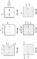
- FIG. 6D illustrates a top view of the reflective layer 40 c .
- the reflective layer 40 c includes a second outer edge 401 c and a second inner edge 402 c .
- the reflective layer 40 c neither outwardly extends to exceed the first outer edge 301 c and/or the first inner edge 302 c of the transparent conductive layer 30 c nor outwardly extends to exceed the first edge E 1 and/or the second edge E 2 of the semiconductor structure 1000 c .
- the first outer edge 301 c of the transparent conductive layer 30 c is disposed between the second outer edge 401 c of the reflective layer 40 c and the first edge E 1
- the first inner edge 302 c is disposed between the second inner edge 402 c and the second edge E 2 .
- the first outer edge 301 c is closer to the first edge E 1 than the second outer edge 401 c to the first edge E 1
- the first inner edge 302 c is closer to the second edge E 2 than the second inner edge 402 c to the second edge E 2
- the reflective layer 40 c covers a part of the top portion f 20 c of the first insulating structure 20 c , such as the top portion f 20 c on the surface 102 s
- the reflective layer 40 c is devoid of covering the side portion s 20 c and the bottom portion t 20 c .
- a part of the transparent conductive layer 30 c near the first edge E 1 and/or the second edge E 2 is located between the reflective layer 40 c and the top portion f 20 c .
- the second outer edge 401 c and/or the second inner edge 402 c are devoid of extending to excess the first outer edge 301 c and/or the first inner edge 302 c respectively.
- the transparent conductive layer 30 c can avoid peeling issue between the reflective layer 40 c and the first insulating structure 20 c .
- the reflective layer 40 c connects to the first insulating structure 20 c via the transparent conductive layer 30 c , and the transparent conductive layer 30 c disposed between them can increase the adhesion between the reflective layer 40 c and the first insulating structure 20 c.
- the second outer edge 401 c is aligned to the first outer edge 301 c of the transparent conductive layer 30 c
- the second inner edge 402 c is aligned to the first inner edge 302 c of the transparent conductive layer 30 c
- the second outer edge 401 c is misaligned with the first edge E 1 and/or the second inner edge 402 c is misaligned with the second edge E 2 .
- neither the reflective layer 40 c nor the transparent conductive layer 30 c extends to cover the side walls, such as the second outside wall 1001 c and the inside wall 1002 c , of the semiconductor structure 1000 c to reduce an electrical short risk in the light-emitting device 1 c that is caused by current leakage through the reflective layer 40 c , the transparent conductive layer 30 c , and the cracks of the first insulating structure 20 c to the semiconductor structure 1000 c .
- the second outside wall 1001 c and the inside wall 1002 c are composed by the side-surfaces of the first semiconductor layer 101 c , the active layer 103 c and the second semiconductor layer 102 c , if the reflective layer 40 c extends to the second outside wall 1001 c and the inside wall 1002 c may cause current leakage when the first insulating structure 20 c having defects or cracks.
- some of metal material of the reflective layer 40 c may diffuse to the first semiconductor layer 101 c and the second semiconductor layer 102 c through the defects or cracks of the first insulating structure 20 c , and therefore a short current is caused due to the electrical connection between the first semiconductor layer 101 c and the second semiconductor layer 102 c via the diffusion of the reflective layer 40 c . Therefore, the reliability of the light-emitting device 1 c would be decreased when the reflective layer 40 c excesses the first edge E 1 and the second edge E 2 and covers the side portion s 20 c .
- the application will not be limited by the embodiments.
- Other producing methods, material of the first insulating structure 20 c or structures of the first insulating structure 20 c such as multiple-insulating layers can be used to improve the quality, mechanical strength of the first insulating structure 20 c to prevent the current short issue.
- the second semiconductor layer 102 c includes a first area
- the reflective layer 40 c includes a second area.
- the first area is defined by the first edge E 1 and the second edge E 2 of the second semiconductor layer 102 c
- the second area is defined by the second outer edge 401 c and the second inner edge 402 c of the reflective layer 40 c .
- the first edge E 1 of the second semiconductor layer 102 c surrounds the second outer edge 401 c of the reflective layer 40 c
- the second inner edge 402 c surrounds the second edge E 2 of the second semiconductor layer 102 c .
- the second area of the reflective layer 40 c is not less than 80% of the first area of the second semiconductor layer 102 c . In one embodiment, the second area is 82%-96% of the first area. In one embodiment, the second area is 85%-95% of the first area.
- a distance D is between the second outer edge 401 c of the reflective layer 40 c and the first edge E 1 of the semiconductor structure 1000 c .
- a distance D′ is between the second inner edge 402 c and the second edge E 2 .
- the distance D or the distance D′ is greater than zero.
- the distance D or the distance D′ is not greater than 10 ⁇ m.
- the distance D or the distance D′ is not greater than 8 ⁇ m.
- the distances D, D′ are greater than 0 ⁇ m and less than 10 ⁇ m.
- the distances D, D′ are between 2 ⁇ m and 8 ⁇ m.
- the distance D and distance D′ could be the same or different.
- the barrier layer 41 c is formed on and covers the reflective layer 40 c .
- An outer edge (not shown) of the barrier layer 41 c surrounds the second outer edge 401 c of the reflective layer 40 c , and/or an inner edge (not shown) of the barrier layer 41 c surrounds the second inner edge 402 c of the reflective layer 40 c .
- the reflective layer 40 c is formed on and covers the barrier layer 41 c .
- the outer edge of the barrier layer 41 c can be surrounded by the second outer edge 401 c of the reflective layer 40 c , and/or the inner edge of the barrier layer 41 c can be surrounded by the second inner edge 402 c of the reflective layer 40 c .
- the outer edge and the inner edge of the barrier layer 41 respectively overlap or align with the second outer edge 401 c and the second inner edge 402 c of the reflective layer 40 c.
- FIGS. 3A-3C respectively illustrate a partial cross-sectional view of the transparent conductive layer 30 c and the reflective layer 40 c near the first edge E 1 or the second edge E 2 of the light-emitting device 1 c in accordance with embodiments of the present application.
- the reflective layer 40 c is formed on the transparent conductive layer 30 c .
- the reflective layer 40 c and the transparent conductive layer 30 c are formed on the first insulating structure 20 c and devoid of extending onto the sidewalls or into the via 100 c of the semiconductor structure 1000 c .
- the reflective layer 40 c and the transparent conductive layer 30 c which are formed on the first insulating structure 20 c , extend onto the sidewalls or into the via 100 c of the semiconductor structure 1000 c.
- the reflective layer 40 c is a discontinuous structure and includes a first reflective portion 403 c and a second reflective portion 404 c separated from the first reflective portion 403 c . There is a gap G between the first reflective portion 403 c and the second reflective portion 404 c .
- the transparent conductive layer 30 c is a discontinuous structure and includes a first conductive portion 31 c and a second conductive portion 32 c separated from the first conductive portion 31 c .
- the second conductive portion 32 c and the second reflective portion 404 c are entirely disposed on the first insulating structure 20 c and the second semiconductor layer 102 c .
- the first conductive portion 31 c and the second conductive portion 32 c locate under the first reflective portion 403 c and the second reflective portion 404 c respectively. Since the first reflective portion 403 c disconnects with the second reflective portion 404 c and the first conductive portion 31 c disconnects with the second conductive portion 32 c , and the second conductive portion 32 c and the second reflective portion 404 c are entirely disposed on the first insulating structure 20 c , the current is unable to flow between the first reflective portion 403 c and the second reflective portion 404 c . That is, the second reflective portion 404 c electrically disconnects to the first reflective portion 403 c.
- the transparent conductive layer 30 c includes a first conductive portion 31 c and a third conductive portion 33 c separated from the first conductive portion 31 c
- the reflective layer 40 c includes a first reflective portion 403 c and a third reflective portion 405 c separated from the first reflective portion 403 c in FIG. 3B .
- the third conductive portion 33 c is formed on the first insulating structure 20 c and the second semiconductor layer 102 c , and extends onto the second outside wall 1001 c to cover the side portion s 20 c and the bottom portion t 20 c of the first insulating structure 20 c .
- the third conductive portion 33 c is formed on the first insulating structure 20 c and the second semiconductor layer 102 c , and extends onto the inside wall 1002 c to cover the side portion s 20 c of the first insulating structure 20 c .
- the first reflective portion 403 c and the third reflective portion 405 c are formed on the first conductive portion 31 c and the third conductive portion 33 c respectively.
- the reflective layer 40 c includes a first reflective portion 403 c ′, a second reflective portion 404 c ′ and a third reflective portion 405 c ′ separated from one another.
- the transparent conductive layer 30 c includes a first conductive portion 31 c ′, the second conductive portion 32 c ′ and a third conductive portion 33 c ′ separated from one another. Therefore, the third reflective portion 405 c ′, the second reflective portion 404 c ′ and the first reflective portion 403 c ′ are electrically insulated from one another.
- each of the reflective layers 40 c is the discontinuous structure and electrically disconnected, the current leakage can be avoided while the reflective layer 40 c extends onto the sidewalls of the semiconductor structure 1000 c to increase the second area of the reflective layer 40 c .
- Both of the reflective area for brightness and the reliability of the individual light-emitting devices have been considered.
- the second area of the reflective layer 40 c is not less than 80% of the first area of the second semiconductor layer 102 c
- the distance D between the first edge E 1 and the second outer edge 401 c is between 0 ⁇ m and 10 ⁇ m.
- the first outer edge 301 c and the second outer edge 401 c are closer to the center of the semiconductor structure 1000 c than the first edge E 1 in the light-emitting device shown in FIG. 3A .
- the first edge E 1 is closer to the center of the semiconductor structure 1000 c than the first outer edge 301 c and the second outer edge 401 c in FIGS. 3B-3C .
- the reflective layer 40 c covers the sidewalls of the semiconductor structure 1000 c in FIGS. 3B-3C
- the second areas of the reflective layer 40 c of the light-emitting device shown in FIGS. 3B-3C are larger than that shown in FIG. 3A .
- FIG. 3C could be larger than that shown in FIG. 3A or FIG. 3B , and thus the brightness of the light-emitting device shown in FIG. 3C can be higher than that of the light-emitting device shown in FIG. 3A or FIG. 3B .
- the reflective layer 40 c includes multiple sub-layers, such as a Distributed Bragg reflector (DBR).
- DBR Distributed Bragg reflector
- the material of the DBR can be electrically isolated or electrically conductive.
- the reflective layer 40 c includes a single layer structure or a multi-layer structure
- the material of the reflective layer 40 c includes a metal material with a high reflectance for the light emitted by the active layer 103 c , such as silver (Ag), gold (Au), aluminum (Al), titanium (Ti), chromium (Cr), copper (Cu), nickel (Ni), platinum (Pt) or an alloy thereof.
- the high reflectance referred to herein means having 80% or more reflectance for a wavelength of a light emitted from the active layer 103 c.
- the reflective structure further includes a DBR structure below the reflective layer 40 c .
- the DBR structure is formed between the semiconductor structure 1000 c and the reflective layer 40 c .
- a connecting layer can be chosen to insert between the DBR structure and the reflective layer 40 c to increase the adhesion between them.
- a first layer is connected to the reflective layer 40 c , wherein the first layer includes silicon oxide (SiO 2 ) and the reflective layer 40 c includes silver (Ag).
- the connecting layer therebetween includes ITO, IZO or the other similar material has higher adhesion to the reflective layer 40 c than the first layer of the DBR structure has.
- the reflective structure further includes the barrier layer 41 c , which covers the reflective layer 40 c to prevent the surface of the reflective layer 40 c from being oxidized that deteriorates the reflectivity of the reflective layer 40 c .
- the material of the barrier layer 41 c includes metal material, such as titanium (Ti), tungsten (W), aluminum (Al), indium (In), tin (Sn), nickel (Ni), platinum (Pt), zinc (Zn), chromium (Cr) or an alloy of the above materials.
- the barrier layer 41 c can include a single layer structure or a multi-layer structure.
- the barrier layer 41 c is alternately stacked by a first barrier layer (not shown) and a second barrier layer (not shown), for example, Cr/Pt, Cr/Ti, Cr/TiW, Cr/W, Cr/Zn, Ti/Pt, Ti/W, Ti/TiW, Ti/W, Ti/Zn, Pt/TiW, Pt/W, Pt/Zn, TiW/W, TiW/Zn, or W/Zn.
- the material of the barrier layer 41 c includes a metal material other than gold (Au) or copper (Cu).
- the second insulating structure 50 c of the light-emitting device 1 c is formed on the semiconductor structure 1000 c by sputtering or vapor deposition.
- the second insulating structure 50 c is formed on the semiconductor structure 1000 c , the first insulating structure 20 c , the transparent conductive layer 30 c and the reflective layer 40 c .
- FIG. 6E illustrates a top view of the second insulating structure 50 c . As shown in FIGS.
- the second insulating structure 50 c includes one or multiple first insulating openings 501 c to expose the second surface 1012 c of the first semiconductor layer 101 c , and one or multiple second insulating openings 502 c to expose the reflective layer 40 c or the barrier layer 41 c .
- the first insulating openings 501 c and the second insulating openings 502 c include different widths or numbers. From the top view of the light-emitting device 1 c , the shapes of the first insulating openings 501 c and the second insulating openings 502 c include circular, elliptical, rectangular, polygonal, or arbitrary shapes.
- the positions of the first insulating openings 501 c are formed to correspond to the positions of the vias 100 c .
- the one second insulating openings 502 c is at one side of the light-emitting device 1 c opposite to the first insulating openings 501 c.
- the second insulating structure 50 c is formed of a non-conductive material and includes organic material, inorganic material or dielectric material.
- the organic material includes Sub, benzocyclobutene (BCB), perfluorocyclobutane (PFCB), epoxy resin, acrylic resin, cyclic olefin polymers (COC), polymethylmethacrylate (PMMA), polyethylene terephthalate (PET), polycarbonate (PC), polyetherimide, or fluorocarbon polymer.
- the inorganic material includes silicone, or glass.
- the dielectric material includes aluminum oxide (Al 2 O 3 ), silicon nitride (SiN x ), silicon oxide (SiO x ), titanium oxide (TiO x ), or magnesium fluoride (MgF x ).
- the second insulating structure 50 c includes one layer or multiple layers.
- the second insulating structure 50 c can be a distributed Bragg reflector (DBR).
- DBR distributed Bragg reflector
- the second insulating structure 50 c can be formed by alternately stacking a SiO x sub-layer and a TiO x sub-layer.
- the material of the second insulating structure 50 c and that of the first insulating structure 20 c can be the same or different.
- FIG. 6G illustrates a top view of the contact layer 60 c .
- the contact layer 60 c is formed on the second insulating structure 50 c and the reflective layer 40 c or on the barrier layer 41 c .
- the contact layer 60 c includes a first contact part 601 c , a second contact part 602 c , and a pin region 600 c electrically separated from one another.
- first contact part 601 c is electrically connected to the first semiconductor layer 101 c
- the second contact part 602 c is electrically connected to the second semiconductor layer 102 c
- the pin region 600 c is electrically isolated from the first contact part 601 c and the second contact part 602 c
- the first contact part 601 c is formed on the first surface 1011 c of the first semiconductor layer 101 c to surround a periphery of the semiconductor structure 1000 c and contact the first semiconductor layer 101 c to form an electrical connection.
- first contact part 601 c includes a peripheral length larger than a peripheral length of the active layer 103 c .
- the first contact part 601 c is also formed on the second surfaces 1012 c of the first semiconductor layer 101 c to cover the one or multiple vias 100 c via the plurality of first insulating openings 501 c of the second insulating structure 50 c and contact the first semiconductor layer 101 c to form an electrical connection.
- the pin region 600 c is deposited on the second semiconductor layer 102 c , and electrically isolated from the first semiconductor layer 101 c and the second semiconductor layer 102 c by the second insulating structure 50 c . In the present embodiment, the pin region 600 c is substantially deposited at the center of the light-emitting device 1 c from the top-view.
- the second contact part 602 c electrically connects the surface 102 s of the second semiconductor layer 102 c via the reflective layer 40 c and the transparent conductive layer 30 c to form an electrical connection between the second contact part 602 c and the second semiconductor layer 102 c .
- the pin region 600 c is located between the first contact part 601 c and the second contact part 602 c .
- the pin region 600 c and the second contact part 602 c are surrounded by the first contact part 601 c as shown in FIG. 6G .
- the pin region 600 c is electrically connected to one of the first contact part 601 c or the second contact part 602 c .
- a shape of the pin region 600 c in a top-view includes a geometric shape, for example, a rectangle or a circle.
- the contact layer 60 c can be a single layer structure or a multi-layer structure.
- the material of the contact layer 60 c includes metal such as aluminum (Al), silver (Ag), chromium (Cr), platinum (Pt), nickel (Ni), titanium (Ti), tungsten (W), or zinc (Zn).
- FIG. 6H illustrates a top view of the third insulating structure 70 c .
- the third insulating structure 70 c includes a first opening 701 c and a second opening 702 c .
- the first opening 701 c exposes the first contact part 601 c of the contact layer 60 c
- the second opening 702 c exposes the second contact part 602 c of the contact layer 60 c .
- the third insulating structure 70 c includes one layer or multiple layers.
- a material of the third insulating structure 70 c includes non-conductive material which includes organic materials, inorganic materials or dielectric material.
- the organic material includes Sub, benzocyclobutene (BCB), perfluorocyclobutane (PFCB), epoxy resin, acrylic resin, cyclic olefin polymers (COC), polymethylmethacrylate (PMMA), polyethylene terephthalate (PET), polycarbonate (PC), polyetherimide, or fluorocarbon polymer.
- the inorganic material includes silicone, or glass.
- the dielectric material includes aluminum oxide (Al 2 O 3 ), silicon nitride (SiN x ), silicon oxide (SiO x ), titanium oxide (TiO x ), or magnesium fluoride (MgF x ).
- the first insulating structure 20 c , the second insulating structure 50 c , and the third insulating structure 70 c can be the same material or different materials selected from the materials described above.
- the first insulating structure 20 c , the second insulating structure 50 c , and the third insulating structure 70 c can be formed by printing, evaporation or sputtering.
- FIG. 6I illustrates a top view of the first pad 80 c and the second pad 90 c .
- the positions and/or shapes of the first pad 80 c and the second pad 90 c also respectively correspond to those of the first opening 701 c and the second opening 702 c of the third insulating structure 70 c .
- the first pad 80 c is electrically connected to the first semiconductor layer 101 c through the first opening 701 c of the third insulating structure 70 c and the first contact part 601 c of the contact layer 60 c
- the second pad 90 c is electrically connected to the second semiconductor layer 102 c through the second opening 702 c of the third insulating structure 70 c , the second contact part 602 c of the contact layer 60 c , the reflective layer 40 c and the transparent conductive layer 30 c .
- the first pad 80 c includes the same shape as that of the second pad 90 c , for example, the first pad 80 c and the second pad 90 c include rectangular shape, but the present disclosure is not limited hereto.
- the shape or the size of the first pad 80 c can be different from that of the second pad 90 c for recognizing the first pad 80 c and the second pad 90 c or for producing a good current spreading in the light-emitting device 1 c .
- the shape of the first pad 80 c can be rectangular, and the shape of the second pad 90 c is comb-shaped, and the area of the first pad 80 c is larger than that of the second pad 90 c .
- the first pad 80 c and the second pad 90 c includes a structure having one or more layers.
- Materials of the first pad 80 c and the second pad 90 c include metal materials, such as chromium (Cr), titanium (Ti), tungsten (W), aluminum (Al), indium (In), tin (Sn), nickel (Ni), platinum (Pt), or an alloy of the above materials.
- the first pad 80 c and the second pad 90 c include a multi-layer structure
- the first pad 80 c and the second pad 90 c includes an upper pad and a lower pad (not shown) respectively.
- the upper pad and the lower pad have different functions. The function of the upper pad is used for soldering or wiring.
- the light-emitting device 1 c can be flipped and mounted on a package substrate (not shown) by using solder bonding or AuSn eutectic bonding through the upper pad.
- the metal material of the upper pad includes highly ductile materials such as nickel (Ni), cobalt (Co), iron (Fe), titanium (Ti), copper (Cu), gold (Au), tungsten (W), zirconium (Zr), molybdenum (Mo), tantalum (Ta), aluminum (Al), silver (Ag), platinum (Pt), palladium (Pd), rhodium (Rh), iridium (Ir), ruthenium (Ru) or osmium (Os).
- the upper pad can be a single layer, or a multilayer film of the above materials.
- the material of the upper pad preferably includes nickel (Ni) and/or gold (Au), or an alloy thereof.
- the function of the lower pad is for forming a stable interface with the contact layer 60 c , the reflective layer 40 c , or the barrier layer 41 c , for example, improving the interface bonding strength between the lower pad and the contact layer 60 c , or enhancing the interface bonding strength between the lower pad of the second pad 90 c and the reflective layer 40 c or the barrier layer 41 c .
- the lower pad can include metal materials different from the upper pad. That is, the material of the lower pad include the material other than gold (Au) and copper (Cu), such as nickel (Ni), cobalt (Co), iron (Fe), titanium (Ti), tungsten (W), zirconium (Zr), molybdenum (Mo), tantalum (Ta), aluminum (Al), silver (Ag), platinum (Pt), palladium (Pd), rhodium (Rh), iridium (Ir), ruthenium (Ru), osmium (Os).
- Au gold
- Cu copper
- the lower pad can be a single layer, an alloy, or a multilayer film of the above materials.
- the lower pad preferably includes a multilayer film of titanium (Ti) and aluminum (Al), or a multilayer film of chromium (Cr) and aluminum (Al).
- FIGS. 6A, 6B ′, 6 C- 6 D, 6 E′, 6 G- 6 I illustrate process flow of the light-emitting device in accordance with another embodiment of the present application.
- the main differences between the light-emitting device in the present embodiment and the light-emitting device 1 c are the structures of the first insulating structure 20 c and the second insulating structure 50 c .
- the first insulating structure 20 c includes a surrounding insulating part 201 c and a plurality of ring-shaped caps 202 c .
- the surrounding insulating part 201 c includes a plurality of protrusions 2011 c and a plurality of recesses 2012 c .
- FIG. 3D illustrates a partial cross-sectional view at one of the protrusions 2011 c of the light-emitting device in accordance with the present embodiment.
- the surrounding insulating part 201 c is disposed along the first surface 1011 c and surrounds the semiconductor structure 1000 c .
- the plurality of protrusions 2011 c and the plurality of recesses 2012 c of the surrounding insulating part 201 c are alternately arranged on the first surface 1011 c .
- the plurality of protrusions 2011 c extends from the surface 102 s of the second semiconductor layer 102 c and covers portions of the first surface 1011 c of the semiconductor structure 1000 c , and the plurality of recesses 2012 c exposes other portions of the first surface 1011 c .
- the first surface 1011 c includes a first exposed area exposed by the surrounding insulating part 201 c , and the first exposed area is discontinuous.
- the second insulating structure 50 c includes a periphery 503 c including a plurality of protrusions 5031 c and a plurality of recesses 5032 c in the present embodiment. As shown in FIG. 3D , the second insulating structure 50 c covers the first insulating structure 20 c , so that the second outside wall 1001 c and a portion of the first surface 1011 c which is covered by the first insulating structure 20 c are also covered by the second insulating structure 50 c .
- the plurality of protrusions 5031 c and the plurality of recesses 5032 c of the second insulating structure 50 c are arranged alternately along the first surface 1011 c of the semiconductor structure 1000 c .
- a shape of the periphery 503 c of second insulating structure 50 c corresponds to a shape of a periphery of the first insulating structure 20 c for discontinuously exposing the first surface 1011 c of the semiconductor structure 1000 c .
- shapes and positions of the plurality of protrusions 5031 c and the plurality of recesses 5032 c respectively correspond to shapes and positions of the plurality of protrusions 2011 c and the plurality of recesses 2012 c of the surrounding insulating part 201 c .
- the first surface 1011 c exposed by the plurality of recesses 2012 c of the first insulating structure 20 c can be also exposed by the plurality of recesses 5032 c of the second insulating structure 50 c .
- the first surface 1011 c covered by the plurality of protrusions 2011 c can be covered by the plurality of protrusions 5031 c .
- the first surface 1011 c includes a second exposed area exposed by the plurality of recesses 5032 c , and the second exposed area is discontinuous.
- the second exposed area of the first surface 1011 c substantially corresponds to the first exposed area exposed by the first insulating structure 20 c .
- the first contact part 601 c is electrically connected to the first semiconductor layer 101 c by contacting the first surface 1011 c via the plurality of recesses 5032 c of the second insulating structure 50 c and the plurality of recesses 2012 c of the first insulating structure 20 c .
- the first contact part 601 c includes a discontinuous contact region (not shown) contact the first surface 1011 c .
- the discontinuous contact region between the first contact part 601 c and the first surface 1011 c of the semiconductor structure 1000 c benefits current spreading of the light-emitting device and avoid breakdown of the light-emitting device.
- FIG. 4A shows a table listing the characteristics of samples A ⁇ B. More specifically, the table shows the characteristics of a conventional light-emitting device (sample A) and the light-emitting device 1 c in one embodiment of the present application (sample B).
- Sample A and sample B include the same shape, which is square, and the same chip size, which is 35 ⁇ 35 mil 2 .
- the differences are the area of the reflective layer of the conventional light-emitting device is smaller than the reflective layer 40 c of the light-emitting device 1 c .
- the distance between the first edge of the second semiconductor layer and the second outer edge of the reflective layer is 15 ⁇ m.
- the distance D of the light-emitting device 1 c in the embodiment is 6 ⁇ m.
- the distance D of the light-emitting device 1 c is smaller than the distance of the conventional light-emitting device.
- the area of the reflective layer 40 c of the light-emitting device 1 c is larger than that of the reflective layer of the conventional light-emitting device.
- a ratio of the area of the reflective layer 40 c to the area of the second semiconductor layer 102 c of the light-emitting device 1 c is larger than a ratio of the area of the reflective layer to the area of the second semiconductor layer of the conventional light-emitting device.
- the table indicates that, the power (I V2 ) of the light-emitting device 1 c is enhanced by 1.8% ( ⁇ I V2 ) compared with that of the conventional light-emitting device, while the forward voltage (V f2 ) and the wavelength (W d2 ) are kept at the same levels. Therefore, the reflective layer 40 c with a larger area can enhance the performance of the light-emitting device 1 c.
- FIG. 4B shows a table listing the characteristics of samples C ⁇ F. More specifically, the table shows the performances of the samples C ⁇ F.
- Sample C is a conventional light-emitting device.
- Sample D is a light-emitting device with the contact layer 60 c including the discontinuous contact region as shown in FIGS. 6B ′ 6 E′ and 3 D but without a larger second area of the reflective layer 40 c as shown in FIGS. 1 ⁇ 2 .
- Sample E is the light-emitting device 1 c with a larger second area of the reflective layer 40 c as shown in FIGS. 1 ⁇ 2 .
- Sample F is the light-emitting device including the contact layer 60 c with the discontinuous contact region shown in FIGS.
- sample D has more advanced performance in the brightness compared with sample C.
- the light-emitting device, sample F has a highest power (I V2 ).
- FIG. 5 illustrates a top view of a light-emitting device 2 c in accordance with an embodiment of the present application.
- FIG. 7 is a cross-sectional view of the light-emitting device 2 c taken along line E-E′ of FIG. 5 .
- 6A-6B, 6C ′, 6 D, 6 E- 6 I respectively show the layouts of the semiconductor structure 1000 c with the exposed first surface 1011 c and the second surface 1012 c of first semiconductor layer 101 c , the first insulating structure 20 c , the transparent conductive layer 30 c , the reflective layer 40 c , the second insulating structure 50 c , an adhesion layer 51 c , the contact layer 60 c , the third insulating structure 70 c and the pads 80 c , 90 c of the light-emitting device 2 c .
- the light-emitting device 2 c in the embodiment is similar to the light-emitting device 1 c shown in FIGS. 1-2 .
- the light-emitting device 2 c further includes the adhesion layer 51 c between the second insulating structure 50 c and the contact layer 60 c .
- the transparent conductive layer 30 c of the light-emitting device 2 c further includes a first transparent conductive portion f 30 c , a second transparent conductive portion s 30 c and a third transparent conductive portion t 30 c separated from one another different from the transparent conductive layer 30 c of the light-emitting device 1 c .
- the material of the second insulating structure 50 c includes silicon oxide (SiO 2 ) and the material of the contact layer 60 c includes silver (Ag), the adhesion layer 51 c between the second insulating structure 50 c and the contact layer 60 c can enhance the adhesion between the second insulating structure 50 c and the contact layer 60 c .
- the adhesion layer 51 c can prevent the contact layer 60 c peeling from the second insulating structure 50 c . Inserting the adhesion layer 51 c therebetween benefits the reliability of the light-emitting device 2 c .
- the adhesion layer 51 c includes a material which has higher adhesion with the second insulating structure 50 c than that between the contact layer 60 c and the second insulating structure 50 c .
- the material of the adhesion layer 51 c can be transparent conductive material or metal.
- the transparent conductive material includes metal oxide.
- the metal oxide includes indium tin oxide (ITO), indium zinc oxide (IZO), indium oxide (InO), tin oxide (SnO), cadmium tin oxide (CTO), antimony tin oxide (ATO), aluminum zinc oxide (AZO), zinc tin oxide (ZTO), gallium doped zinc oxide (GZO), tungsten doped indium oxide (IWO) or zinc oxide (ZnO).
- the metal includes Pt.
- the material of the adhesion layer 51 c is not limited to the above material.
- a shape and an area of the adhesion layer 51 c shown in FIG. 6F is similar to that of the second insulating structure 50 c shown in FIG. 6E .
- the adhesion layer 51 c includes one or multiple first adhesion openings 511 c corresponding to the first insulating openings 501 c and one or multiple second adhesion openings 512 c corresponding to the second insulating openings 502 c .
- a periphery 513 c of the adhesion layer 51 c surrounds a periphery 503 c of the second insulating structure 50 c for electrically connecting to the first surface 1011 c of the first semiconductor layer 101 c .
- the adhesion layer 51 c extends onto the exposed part of the semiconductor structure 1000 c . More specifically, the adhesion layer 51 c extends onto the first surface 1011 c and/or the second surface 1012 c as shown in FIG. 7 .
- the first transparent conductive portion f 30 c is located on the surface 102 s of the second semiconductor layer 102 c
- the second transparent conductive portion s 30 c is located on the first surface 1011 c of the exposed part
- the third transparent conductive portion t 30 c is located on the second surface 1012 c of the exposed part in the via 100 c .
- the transparent conductive layer 30 c connects to the adhesion layer 51 c on the exposed part.
- the third transparent conductive portion t 30 c is surrounded by the first transparent conductive portion f 30 c , and the first transparent conductive portion f 30 c is surrounded by the second transparent conductive portion s 30 c in a top view of the transparent conductive layer 30 c as shown in FIG. 6C ′.
- the area of the first transparent conductive portion f 30 c is larger than the second transparent conductive portion s 30 c and the third transparent conductive portion t 30 c .
- the first transparent conductive portion f 30 c includes a first periphery f 30 c 1
- the second transparent conductive portion s 30 c includes a second periphery s 30 c 1 surrounding the first periphery f 30 c 1
- the third transparent conductive portion t 30 c includes a third periphery t 30 c 1 surrounded by the first periphery f 30 c 1 in the top view.
- the reflective layer 40 c formed on the first transparent conductive portion f 30 c .
- the reflective layer 40 c includes a second outer edge 401 c and a second inner edge 402 c surrounded by the second outer edge 401 c .
- the reflective layer 40 c neither outwardly extends to exceed the first outer edge 301 c and/or the first inner edge 302 c of the transparent conductive layer 30 c nor outwardly extends to exceed the first edge E 1 and/or the second edge E 2 of the semiconductor structure 1000 c .
- the second outer edge 401 c is substantially aligned to the first outer edge 301 c
- the second inner edge 402 c is substantially aligned to the first inner edge 302 c
- the second insulating structure 50 c is formed on the reflective layer 40 c , and covers the first insulating structure 20 c .
- the second insulating structure 50 c including the plurality of protrusions 5031 c and the plurality of recesses 5032 c as shown in FIG. 6E ′ are located on the exposed part of the semiconductor structure 1000 c and covers the first surface 1011 c or the transparent conductive layer 30 c shown in FIGS. 6C and 6C ′.
- the plurality of protrusions 5031 c and the plurality of recesses 5032 c are arranged alternately along the first surface 1011 c , and discontinuously covers the first surface 1011 c . More specifically, the plurality of protrusions 5031 c covers portions of the first surface 1011 c which is covered by the plurality of protrusions 2011 c , and the plurality of recesses 5032 c exposes portions of the first surface 1011 c which is exposed by the plurality of recesses 2012 c . In one embodiment, the plurality of protrusions 5031 c covers portions of the second transparent conductive portion s 30 c and the plurality of recesses 5032 c exposes portions of the second transparent conductive portion s 30 c.
- the light-emitting device 2 c includes the contact layer 60 c having the first contact part 601 c , the second contact part 602 c and the pin region 600 c .
- the first contact part 601 c electrically connects to the first semiconductor layer 101 c through the first adhesion opening 511 c , the first insulating openings 501 c and the second transparent conductive portion s 30 c disposed on the first surface 1011 c and the third transparent conductive portion t 30 c disposed on the second surface 1012 c in the vias 100 c .
- the second contact part 602 c electrically connects to the second semiconductor layer 102 c through the second adhesion openings 512 c , and the second insulating openings 502 c , the reflective layer 40 c and the first transparent conductive portion f 30 c disposed on the surface 102 s of the second semiconductor layer 102 c .
- the material of the first contact part 601 c and the second contact part 602 c are the same and both of them are multi-layer structure.
- the first contact part 601 c includes a first portion and the second portion covered the first portion.
- the material of the first portion includes Ag/NiTi/TiW/Pt and the material of the second portion includes Ti/Al/Ti/Al/Cr/Pt sequentially formed on the semiconductor structure 1000 c in a direction from the semiconductor stack 10 c to the second pad 90 c .
- the second contact part 602 c also includes a first portion and a second portion similar with the first contact part 601 c .
- the material of the first portion and the second portion of the second contact part 602 c can be the same with that of the first contact part 601 c .
- the reflective structure and the first contact part 601 c include a same material with high reflectivity.
- the reflective structure and the second contact part 602 c include a same material with high reflectivity.
- the reflective structure, the first contact part 601 c , and the second contact part 602 c include silver.
- the light-emitting device 2 c includes the second transparent conductive portion s 20 c and the third transparent conductive portion t 30 c between the contact layer 60 c and the first semiconductor layer 101 c , both of the first contact part 601 c and the second contact part 602 c including silver, and the adhesion layer 51 c between the contact layer 60 c and the second insulating structure 50 c .
- the conventional light-emitting device is similar to the Sample C mentioned above and includes a first contact part without silver.
- the material of the first contact part of the conventional light-emitting device includes Cr/Al/Cr/Al/Cr/Pt sequentially formed on a semiconductor structure 1000 c .
- the light-emitting device 2 c in the present embodiment has higher brightness caused by the first contact part 601 c with silver to increase the reflective area of the light-emitting device 2 c , and thus the brightness of the light-emitting device 2 c could be enhanced.
- the brightness (I V2 ) of the conventional light-emitting device is 923.75 mW and the brightness (I V2 ) of the light-emitting device 2 c in the embodiment is 965.83 mW. Therefore, the brightness of the light-emitting device 2 c in the embodiment is increased by 4.56% higher than the conventional light-emitting device.
- FIG. 8 is a schematic view of a light-emitting apparatus 3 in accordance with an embodiment of the present application.
- the light-emitting device can be selected from the foregoing embodiments, and is mounted on the first spacer 511 and the second spacer 512 of the package substrate 51 in the form of flip chip.
- the first spacer 511 and the second spacer 512 are electrically insulated from each other by an insulating portion 53 including an insulating material.
- the main light-extraction surface of the flip-chip is one side of the growth substrates opposite to the pad-forming surface.
- a reflective structure 54 can be provided around the light-emitting device to increase the light extraction efficiency of the light-emitting apparatus 3 .
- FIG. 9 illustrates a structure diagram of a light-emitting apparatus 4 in accordance with an embodiment of the present application.
- a light bulb includes an envelope 602 , a lens 604 , a light-emitting module 610 , a base 612 , a heat sink 614 , a connector 616 and an electrical connecting device 618 .
- the light-emitting module 610 includes a submount 606 and a plurality of light-emitting devices 608 on the submount 606 , wherein the plurality of light-emitting devices 608 can be the light-emitting devices or the light-emitting apparatus 3 described in above embodiments.
Landscapes
- Led Devices (AREA)
- Surgical Instruments (AREA)
- Led Device Packages (AREA)
- Electrodes Of Semiconductors (AREA)
Abstract
A light-emitting device comprises a semiconductor structure comprising a surface and a side wall inclined to the surface, wherein the semiconductor structure comprises a first semiconductor layer, a second semiconductor layer on the first semiconductor layer, and an active layer between the first semiconductor layer and the second semiconductor layer, and the second semiconductor layer comprises a first edge and a first area; a reflective layer located on the second semiconductor layer and comprising an outer edge and a second area, wherein a distance between the first edge and the outer edge is greater than 0 μm and is not greater than 10 μm; and a first contact part comprising a metal formed on the reflective layer and the first semiconductor layer, wherein the first contact part comprises a first periphery comprising a first periphery length larger than a periphery length of the active layer from a top-view of the light-emitting device.
Description
This application is a continuation application of U.S. patent application Ser. No. 16/416,488, filed on May 20, 2019, now pending, which is a continuation application of U.S. patent application Ser. No. 15/874,398, filed on Jan. 18, 2018, which claims priority of U.S. Provisional Application No. 62/450,860 filed on Jan. 26, 2017 under 35 U.S.C. § 119(e), the entire content of which is hereby incorporated by reference.
The application relates to a structure of a light-emitting device, and more particularly, to a light-emitting device including a semiconductor stack and a reflective layer on the semiconductor stack.
Light-Emitting Diode (LED) is a solid-state semiconductor light-emitting device, which has the advantages of low power consumption, low heat generation, long working lifetime, shockproof, small volume, fast reaction speed and good photoelectric property, such as stable emission wavelength. Therefore, light-emitting diodes are widely used in household appliances, equipment indicators, and optoelectronic products.
A light-emitting device includes a semiconductor structure comprising a surface and a side wall inclined to the surface, wherein the semiconductor structure comprises a first semiconductor layer, a second semiconductor layer on the first semiconductor layer, and an active layer between the first semiconductor layer and the second semiconductor layer, and the second semiconductor layer comprises a first edge and a first area; and a reflective layer located on the semiconductor structure and comprising an outer edge and a second area; wherein a distance between the first edge and the outer edge is between 0 μm and 10 μm, and the second area of the reflective layer is not less than 80% of the first area of the second semiconductor layer.
A light-emitting device includes a semiconductor structure comprising a surface and a side wall inclined to the surface, wherein the semiconductor structure comprises a first semiconductor layer, a second semiconductor layer on the first semiconductor layer, and an active layer between the first semiconductor layer and the second semiconductor layer; a first insulating structure located on the surface and the side wall of the semiconductor structure; and a reflective layer comprising a first reflective portion and a second reflective portion separated from the first reflective portion, wherein the first reflective portion located on the second semiconductor layer and second reflective portion located on the first insulating structure.
A light-emitting device includes a semiconductor structure comprising a first semiconductor layer, a second semiconductor layer on the first semiconductor layer, and an active layer between the first semiconductor layer and the second semiconductor layer; wherein the semiconductor structure comprises an exposed part exposing the first semiconductor layer; and a second insulating layer covering the semiconductor structure; a contact layer on the second insulating layer; and a transparent conductive layer located on the second semiconductor layer and the exposed part, and between the first semiconductor layer and the contact layer.
A light-emitting device comprises a semiconductor structure comprising a surface and a side wall inclined to the surface, wherein the semiconductor structure comprises a first semiconductor layer, a second semiconductor layer on the first semiconductor layer, and an active layer between the first semiconductor layer and the second semiconductor layer, and the second semiconductor layer comprises a first edge and a first area; a reflective layer located on the second semiconductor layer and comprising an outer edge and a second area, wherein a distance between the first edge and the outer edge is greater than 0 μm and is not greater than 10 μm; and a first contact part comprising a metal formed on the reflective layer and the first semiconductor layer, wherein the first contact part comprises a first periphery comprising a first periphery length larger than a periphery length of the active layer from a top-view of the light-emitting device.
The embodiment of the application is illustrated in detail, and is plotted in the drawings. The same or the similar part is illustrated in the drawings and the specification with the same or the similar number.
In an embodiment of the present application, the substrate 11 c includes a patterned surface. The patterned surface includes a plurality of projections. A shape of the projection includes taper or cone. The projection can enhance the light-extraction efficiency of the light-emitting device. In an embodiment of the present application, the substrate 11 c can be a growth substrate, such as gallium arsenide (GaAs) wafer for growing aluminum gallium indium phosphide (AlGaInP), sapphire (Al2O3) wafer, gallium nitride (GaN) wafer or silicon carbide (SiC) wafer for growing gallium nitride (GaN) or indium gallium nitride (InGaN). The semiconductor stack 10 c can be formed of group III nitride based compound semiconductor on the substrate 11 c by metal organic chemical vapor deposition (MOCVD), molecular beam epitaxy (MBE), physical vapor deposition (PVD), hydride vapor deposition (HVPE), or ion plating, such as sputtering or evaporation. Moreover, a buffer structure (not shown) can be formed before forming the semiconductor stack 10 c so as to relieve lattice mismatch between the substrate 11 c and the semiconductor stack 10 c and can be formed of a GaN-based material layer, such as gallium nitride or aluminum gallium nitride, or an AlN-based material layer, such as aluminum nitride. The buffer structure can be a single layer or multiple layers. The buffer structure can be formed by metal organic chemical vapor deposition (MOCVD), molecular beam epitaxy (MBE) or physical vapor deposition (PVD). The PVD method includes a sputtering method, for example, reactive sputtering method or evaporation method, such as e-beam evaporation method or thermal evaporation method. In one embodiment, the buffer structure includes an AlN buffer layer and is formed by the sputtering method. The AlN buffer layer is formed on a growth substrate with a patterned surface. The sputtering method can produce a dense buffer layer with high uniformity, and therefore the AN buffer layer can conformably deposit on the patterned surface of the substrate 11 c.
In an embodiment of the present application, the semiconductor stack 10 c includes optical characteristics, such as light-emitting angle or wavelength distribution, and electrical characteristics, such as forward voltage or reverse current. In an embodiment of the present application, the first semiconductor layer 101 c and the second semiconductor layer 102 c, such as a cladding layer or a confinement layer, have different conductivity types, electrical properties, polarities, or doping elements for providing electrons or holes. For example, the first semiconductor layer 101 c is an n-type semiconductor, and the second semiconductor layer 102 c is a p-type semiconductor. The active layer 103 c is formed between the first semiconductor layer 101 c and the second semiconductor layer 102 c. The electrons and holes combine in the active layer 103 c under a current driving to convert electric energy into light energy and then light is emitted from the active layer 103 c. The wavelength of the light emitted from the light-emitting device 1 c is adjusted by changing the physical and chemical composition of one or more layers in the semiconductor stack 10 c. The material of the semiconductor stack 10 c includes a group III-V semiconductor material, such as AlxInyGa(1-x-y)N or AlxInyGa(1-x-y)P, wherein 0≤x, y≤1, and (x+y)≤1. According to the material of the active layer 103 c, when the material of the semiconductor stack 10 c is AlInGaP series material, red light having a wavelength between 610 nm and 650 nm or yellow light having a wavelength between 550 nm and 570 nm can be emitted. When the material of the semiconductor stack 10 c is InGaN series material, blue or deep blue light having a wavelength between 400 nm and 490 nm or green light having a wavelength between 490 nm and 550 nm can be emitted. When the material of the semiconductor stack 10 c is AlGaN series material, UV light having a wavelength between 400 nm and 250 nm can be emitted. The active layer 103 c can be a single heterostructure (SH), a double heterostructure (DH), a double-side double heterostructure (DDH), or a multi-quantum well structure (MQW). The material of the active layer 103 c can be i-type, p-type, or n-type semiconductor.
Referring to FIG. 2 , in an embodiment, the semiconductor structures 1000 c includes a first outside wall 1003 c and a second outside wall 1001 c, wherein one end of the first surface 1011 c of the first semiconductor layer 101 c connects the first outside wall 1003 c and another end of the first surface 1011 c connects the second outside wall 1001 c. The second outside wall 1001 c includes the side-surfaces of the first semiconductor layer 101 c, the active layer 103 c and the second semiconductor layer 102 c. In the present embodiment, the second outside wall 1001 c is composed by the side-surfaces of the first semiconductor layer 101 c, the active layer 103 c and the second semiconductor layer 102 c. The first outside wall 1003 c locates between the first surface 1011 c and the substrate 11 c. In one embodiment, the first outside wall 1003 c and the second outside wall 1001 c are inclined to the first surface 1011 c of the first semiconductor layer 101 c. In one embodiment, the first outside wall 1003 c is inclined to the exposed surface 11 s of the substrate 11 c. An angle between the first outside wall 1003 c and the exposed surface 11 s is an acute angle. In one embodiment, an angle between the first outside wall 1003 c and the exposed surface 11 s is an obtuse angle.
The semiconductor stack 10 c further includes an inside wall 1002 c. Similar to the second outside wall 1001 c, the inside wall 1002 c is composed by side-surfaces of the first semiconductor layer 101 c, the active layer 103 c and the second semiconductor layer 102 c at the via 100 c. In an embodiment of the present application, the via 100 c is defined by the inside wall 1002 c and the second surfaces 1012 c of the first semiconductor layer 101 c. One end of the inside wall 1002 c is connected to the second surface 1012 c of the first semiconductor layer 101 c and another end of the inside wall 1002 c is connected to a surface 102 s of the second semiconductor layer 102 c. The surface 102 s of the second semiconductor layer 102 c is substantially perpendicular to the stacking direction. The inside wall 1002 c and the second outside wall 1001 c are inclined to the surface 102 s of the second semiconductor layer 102 c, and the inside wall 1002 c is also inclined to the second surface 1012 c of the first semiconductor layer 101 c. An angle between the inside wall 1002 c and the second surface 1012 c is an acute angle or an obtuse angle, and an angle between the second outside wall 1001 c and the first surface 1011 c is an acute angle or an obtuse angle. The angle between the second outside wall 1001 c and the surface 102 s is about 100 degrees˜140 degrees, similar to the angle between the inside wall 1002 c and the surface 102 s. Besides, the semiconductor structures 1000 c further includes a first edge E1, which is an intersection of the second outside wall 1001 c and the surface 102 s of the second semiconductor layer 102 c, and a second edge E2, which is an interconnection of the inside wall 1002 c and the surface 102 s of the second semiconductor layer 102 c. In a top view, the second semiconductor layer 102 includes the first edge E1. More specifically, the first edge E1 is a contour of the surface 102 s of the second semiconductor layer 102, and the second edge E2 is a contour of the via 100 c in the top view of the light-emitting device 1 c. In one embodiment, the first edge E1 or the second edge E2 is closed. In one embodiment, the second edge E2 is surrounded by the first edge E1.
The quality of the first insulating structure 20 c might be affected by the process ability or stress. Some cracks might be produced in the first insulating structure 20 c. In one embodiment, the transparent conductive layer 30 c is located on the surface 102 s and devoid of extending to cover the second outside wall 1001 c and the inside wall 1002 c to reduce a risk that short current occurs between the transparent conductive layer 30 c and the semiconductor stack 10 c caused by current leakage from the cracks of the first insulating structure 20 c. Therefore, the reliability of the light-emitting device 1 c can be consistent. Since the transparent conductive layer 30 c is substantially formed on entire of the surface 102 s of the second semiconductor layer 102 c and contacts the second semiconductor layer 102 c, the current can be uniformly spread throughout entire the second semiconductor layer 102 c by the transparent conductive layer 30 c.
The material of the transparent conductive layer 30 c includes a material being transparent to the light emitted from the active layer 103 c, such as metal oxide. The metal oxide includes indium tin oxide (ITO), indium zinc oxide (IZO), indium oxide (InO), tin oxide (SnO), cadmium tin oxide (CTO), antimony tin oxide (ATO), aluminum zinc oxide (AZO), zinc tin oxide (ZTO), gallium doped zinc oxide (GZO), tungsten doped indium oxide (IWO) or zinc oxide (ZnO). The transparent conductive layer 30 c can be configured to form a low-resistance contact, for example, ohmic contact, with the second semiconductor layer 102 c. The transparent conductive layer 30 c includes a single layer or multiple layers. For example, as the transparent conductive layer 30 c includes multiple sub-layers, the transparent conductive layer 30 c can be a distributed Bragg reflector (DBR). In the embodiment, the DBR of the transparent conductive layer 30 c is electrically conductive. In one embodiment, in a top view, a shape of the transparent conductive layer 30 c substantially corresponds to a shape of the second semiconductor layer 102 c. Please refer to FIGS. 6A and 6C , the shape of the transparent conductive layer 30 c shown in FIG. 6C substantially corresponds to the shape of the second semiconductor layer 102 c shown in FIG. 6A .
In an embodiment of the present application, the reflective structure of the light-emitting device 1 c is formed on the transparent conductive layer 30 c. The reflective structure includes the reflective layer 40 c, the barrier layer 41 c or a combination of the above. In one embodiment, in a top view, a shape of the reflective layer 40 c substantially corresponds to a shape of the second semiconductor layer 102 c. FIG. 6D illustrates a top view of the reflective layer 40 c. As shown in FIGS. 1, 2, and 6D , the reflective layer 40 c includes a second outer edge 401 c and a second inner edge 402 c. In the embodiment, the reflective layer 40 c neither outwardly extends to exceed the first outer edge 301 c and/or the first inner edge 302 c of the transparent conductive layer 30 c nor outwardly extends to exceed the first edge E1 and/or the second edge E2 of the semiconductor structure 1000 c. The first outer edge 301 c of the transparent conductive layer 30 c is disposed between the second outer edge 401 c of the reflective layer 40 c and the first edge E1, and/or the first inner edge 302 c is disposed between the second inner edge 402 c and the second edge E2. In other words, the first outer edge 301 c is closer to the first edge E1 than the second outer edge 401 c to the first edge E1, and the first inner edge 302 c is closer to the second edge E2 than the second inner edge 402 c to the second edge E2. In one embodiment, the reflective layer 40 c covers a part of the top portion f20 c of the first insulating structure 20 c, such as the top portion f20 c on the surface 102 s, and the reflective layer 40 c is devoid of covering the side portion s20 c and the bottom portion t20 c. Beside, a part of the transparent conductive layer 30 c near the first edge E1 and/or the second edge E2 is located between the reflective layer 40 c and the top portion f20 c. Specifically, the second outer edge 401 c and/or the second inner edge 402 c are devoid of extending to excess the first outer edge 301 c and/or the first inner edge 302 c respectively. In one embodiment, the transparent conductive layer 30 c can avoid peeling issue between the reflective layer 40 c and the first insulating structure 20 c. More specifically, the reflective layer 40 c connects to the first insulating structure 20 c via the transparent conductive layer 30 c, and the transparent conductive layer 30 c disposed between them can increase the adhesion between the reflective layer 40 c and the first insulating structure 20 c.
In one embodiment, the second outer edge 401 c is aligned to the first outer edge 301 c of the transparent conductive layer 30 c, and/or the second inner edge 402 c is aligned to the first inner edge 302 c of the transparent conductive layer 30 c. In one embodiment, the second outer edge 401 c is misaligned with the first edge E1 and/or the second inner edge 402 c is misaligned with the second edge E2.
In one embodiment, neither the reflective layer 40 c nor the transparent conductive layer 30 c extends to cover the side walls, such as the second outside wall 1001 c and the inside wall 1002 c, of the semiconductor structure 1000 c to reduce an electrical short risk in the light-emitting device 1 c that is caused by current leakage through the reflective layer 40 c, the transparent conductive layer 30 c, and the cracks of the first insulating structure 20 c to the semiconductor structure 1000 c. More specifically, since the second outside wall 1001 c and the inside wall 1002 c are composed by the side-surfaces of the first semiconductor layer 101 c, the active layer 103 c and the second semiconductor layer 102 c, if the reflective layer 40 c extends to the second outside wall 1001 c and the inside wall 1002 c may cause current leakage when the first insulating structure 20 c having defects or cracks. More specifically, some of metal material of the reflective layer 40 c (such as silver, aluminum) may diffuse to the first semiconductor layer 101 c and the second semiconductor layer 102 c through the defects or cracks of the first insulating structure 20 c, and therefore a short current is caused due to the electrical connection between the first semiconductor layer 101 c and the second semiconductor layer 102 c via the diffusion of the reflective layer 40 c. Therefore, the reliability of the light-emitting device 1 c would be decreased when the reflective layer 40 c excesses the first edge E1 and the second edge E2 and covers the side portion s20 c. However, the application will not be limited by the embodiments. Other producing methods, material of the first insulating structure 20 c or structures of the first insulating structure 20 c such as multiple-insulating layers can be used to improve the quality, mechanical strength of the first insulating structure 20 c to prevent the current short issue.
In one embodiment, from the top view of the light-emitting device 1 c, the second semiconductor layer 102 c includes a first area, and the reflective layer 40 c includes a second area. In the embodiment, from the top view of the light-emitting device 1 c, the first area is defined by the first edge E1 and the second edge E2 of the second semiconductor layer 102 c, and the second area is defined by the second outer edge 401 c and the second inner edge 402 c of the reflective layer 40 c. The first edge E1 of the second semiconductor layer 102 c surrounds the second outer edge 401 c of the reflective layer 40 c, and the second inner edge 402 c surrounds the second edge E2 of the second semiconductor layer 102 c. In order to enhance the brightness of the light-emitting device 1 c, the more light emitted from the active layer 103 c can be reflected by the reflective layer 40 c, the more brightness can be enhanced. So the second area of the reflective layer 40 c should be designed as large as possible. A tradeoff between the brightness and the reliability of the light-emitting device 1 c has to be considered. In one embodiment, the second area of the reflective layer 40 c is not less than 80% of the first area of the second semiconductor layer 102 c. In one embodiment, the second area is 82%-96% of the first area. In one embodiment, the second area is 85%-95% of the first area.
In other embodiment, a distance D is between the second outer edge 401 c of the reflective layer 40 c and the first edge E1 of the semiconductor structure 1000 c. A distance D′ is between the second inner edge 402 c and the second edge E2. In one embodiment, the distance D or the distance D′ is greater than zero. In one embodiment, the distance D or the distance D′ is not greater than 10 μm. In one embodiment, the distance D or the distance D′ is not greater than 8 μm. In the embodiment, the distances D, D′ are greater than 0 μm and less than 10 μm. In one embodiment, the distances D, D′ are between 2 μm and 8 μm. Furthermore, in other embodiment, the distance D and distance D′ could be the same or different.
In one embodiment, the barrier layer 41 c is formed on and covers the reflective layer 40 c. An outer edge (not shown) of the barrier layer 41 c surrounds the second outer edge 401 c of the reflective layer 40 c, and/or an inner edge (not shown) of the barrier layer 41 c surrounds the second inner edge 402 c of the reflective layer 40 c. In one embodiment, the reflective layer 40 c is formed on and covers the barrier layer 41 c. The outer edge of the barrier layer 41 c can be surrounded by the second outer edge 401 c of the reflective layer 40 c, and/or the inner edge of the barrier layer 41 c can be surrounded by the second inner edge 402 c of the reflective layer 40 c. In one embodiment, the outer edge and the inner edge of the barrier layer 41 respectively overlap or align with the second outer edge 401 c and the second inner edge 402 c of the reflective layer 40 c.
In one embodiment, as shown in FIG. 3A , the reflective layer 40 c is a discontinuous structure and includes a first reflective portion 403 c and a second reflective portion 404 c separated from the first reflective portion 403 c. There is a gap G between the first reflective portion 403 c and the second reflective portion 404 c. In one embodiment, as shown in FIG. 3A , the transparent conductive layer 30 c is a discontinuous structure and includes a first conductive portion 31 c and a second conductive portion 32 c separated from the first conductive portion 31 c. The second conductive portion 32 c and the second reflective portion 404 c are entirely disposed on the first insulating structure 20 c and the second semiconductor layer 102 c. In one embodiment, the first conductive portion 31 c and the second conductive portion 32 c locate under the first reflective portion 403 c and the second reflective portion 404 c respectively. Since the first reflective portion 403 c disconnects with the second reflective portion 404 c and the first conductive portion 31 c disconnects with the second conductive portion 32 c, and the second conductive portion 32 c and the second reflective portion 404 c are entirely disposed on the first insulating structure 20 c, the current is unable to flow between the first reflective portion 403 c and the second reflective portion 404 c. That is, the second reflective portion 404 c electrically disconnects to the first reflective portion 403 c.
In the embodiment shown in FIG. 3B , the differences between the embodiment in FIG. 3B and the embodiment in FIG. 3A are the transparent conductive layer 30 c includes a first conductive portion 31 c and a third conductive portion 33 c separated from the first conductive portion 31 c, and the reflective layer 40 c includes a first reflective portion 403 c and a third reflective portion 405 c separated from the first reflective portion 403 c in FIG. 3B . There is a gap G between the first reflective portion 403 c and the third reflective portion 405 c. Therefore, the third reflective portion 405 c, and the first reflective portion 403 c are electrically insulated from each other. More specifically, the third conductive portion 33 c is formed on the first insulating structure 20 c and the second semiconductor layer 102 c, and extends onto the second outside wall 1001 c to cover the side portion s20 c and the bottom portion t20 c of the first insulating structure 20 c. In one embodiment, the third conductive portion 33 c is formed on the first insulating structure 20 c and the second semiconductor layer 102 c, and extends onto the inside wall 1002 c to cover the side portion s20 c of the first insulating structure 20 c. The first reflective portion 403 c and the third reflective portion 405 c are formed on the first conductive portion 31 c and the third conductive portion 33 c respectively.
In one embodiment, as shown in FIG. 3C , the reflective layer 40 c includes a first reflective portion 403 c′, a second reflective portion 404 c′ and a third reflective portion 405 c′ separated from one another. Besides, the transparent conductive layer 30 c includes a first conductive portion 31 c′, the second conductive portion 32 c′ and a third conductive portion 33 c′ separated from one another. Therefore, the third reflective portion 405 c′, the second reflective portion 404 c′ and the first reflective portion 403 c′ are electrically insulated from one another. In individual light-emitting devices in accordance with the embodiments shown in FIGS. 3A-3C , each of the reflective layers 40 c is the discontinuous structure and electrically disconnected, the current leakage can be avoided while the reflective layer 40 c extends onto the sidewalls of the semiconductor structure 1000 c to increase the second area of the reflective layer 40 c. Both of the reflective area for brightness and the reliability of the individual light-emitting devices have been considered. In one embodiment, the light-emitting devices shown in FIGS. 3A-3C , the second area of the reflective layer 40 c is not less than 80% of the first area of the second semiconductor layer 102 c, and the distance D between the first edge E1 and the second outer edge 401 c is between 0 μm and 10 μm. In one embodiment, the first outer edge 301 c and the second outer edge 401 c are closer to the center of the semiconductor structure 1000 c than the first edge E1 in the light-emitting device shown in FIG. 3A . The first edge E1 is closer to the center of the semiconductor structure 1000 c than the first outer edge 301 c and the second outer edge 401 c in FIGS. 3B-3C . Since the reflective layer 40 c covers the sidewalls of the semiconductor structure 1000 c in FIGS. 3B-3C , the second areas of the reflective layer 40 c of the light-emitting device shown in FIGS. 3B-3C are larger than that shown in FIG. 3A . Besides, the second area of the reflective layer 40 c shown in FIG. 3C could be larger than that shown in FIG. 3A or FIG. 3B , and thus the brightness of the light-emitting device shown in FIG. 3C can be higher than that of the light-emitting device shown in FIG. 3A or FIG. 3B .
In an embodiment of the present application, the reflective layer 40 c includes multiple sub-layers, such as a Distributed Bragg reflector (DBR). In the embodiment, the material of the DBR can be electrically isolated or electrically conductive.
In an embodiment of the present application, the reflective layer 40 c includes a single layer structure or a multi-layer structure, and the material of the reflective layer 40 c includes a metal material with a high reflectance for the light emitted by the active layer 103 c, such as silver (Ag), gold (Au), aluminum (Al), titanium (Ti), chromium (Cr), copper (Cu), nickel (Ni), platinum (Pt) or an alloy thereof. The high reflectance referred to herein means having 80% or more reflectance for a wavelength of a light emitted from the active layer 103 c.
In an embodiment of the present application, the reflective structure further includes a DBR structure below the reflective layer 40 c. In one embodiment, the DBR structure is formed between the semiconductor structure 1000 c and the reflective layer 40 c. A connecting layer can be chosen to insert between the DBR structure and the reflective layer 40 c to increase the adhesion between them. For example, in the DBR structure, a first layer is connected to the reflective layer 40 c, wherein the first layer includes silicon oxide (SiO2) and the reflective layer 40 c includes silver (Ag). The connecting layer therebetween includes ITO, IZO or the other similar material has higher adhesion to the reflective layer 40 c than the first layer of the DBR structure has.
In an embodiment of the present application, the reflective structure further includes the barrier layer 41 c, which covers the reflective layer 40 c to prevent the surface of the reflective layer 40 c from being oxidized that deteriorates the reflectivity of the reflective layer 40 c. The material of the barrier layer 41 c includes metal material, such as titanium (Ti), tungsten (W), aluminum (Al), indium (In), tin (Sn), nickel (Ni), platinum (Pt), zinc (Zn), chromium (Cr) or an alloy of the above materials. The barrier layer 41 c can include a single layer structure or a multi-layer structure. When the barrier layer 41 c is the multi-layer structure, the barrier layer 41 c is alternately stacked by a first barrier layer (not shown) and a second barrier layer (not shown), for example, Cr/Pt, Cr/Ti, Cr/TiW, Cr/W, Cr/Zn, Ti/Pt, Ti/W, Ti/TiW, Ti/W, Ti/Zn, Pt/TiW, Pt/W, Pt/Zn, TiW/W, TiW/Zn, or W/Zn. In one embodiment, the material of the barrier layer 41 c includes a metal material other than gold (Au) or copper (Cu).
In an embodiment of the present application, the second insulating structure 50 c of the light-emitting device 1 c is formed on the semiconductor structure 1000 c by sputtering or vapor deposition. The second insulating structure 50 c is formed on the semiconductor structure 1000 c, the first insulating structure 20 c, the transparent conductive layer 30 c and the reflective layer 40 c. FIG. 6E . illustrates a top view of the second insulating structure 50 c. As shown in FIGS. 1, 2, and 6E , the second insulating structure 50 c includes one or multiple first insulating openings 501 c to expose the second surface 1012 c of the first semiconductor layer 101 c, and one or multiple second insulating openings 502 c to expose the reflective layer 40 c or the barrier layer 41 c. In an embodiment, the first insulating openings 501 c and the second insulating openings 502 c include different widths or numbers. From the top view of the light-emitting device 1 c, the shapes of the first insulating openings 501 c and the second insulating openings 502 c include circular, elliptical, rectangular, polygonal, or arbitrary shapes. In one embodiment, the positions of the first insulating openings 501 c are formed to correspond to the positions of the vias 100 c. In the embodiment, the one second insulating openings 502 c is at one side of the light-emitting device 1 c opposite to the first insulating openings 501 c.
The second insulating structure 50 c is formed of a non-conductive material and includes organic material, inorganic material or dielectric material. The organic material includes Sub, benzocyclobutene (BCB), perfluorocyclobutane (PFCB), epoxy resin, acrylic resin, cyclic olefin polymers (COC), polymethylmethacrylate (PMMA), polyethylene terephthalate (PET), polycarbonate (PC), polyetherimide, or fluorocarbon polymer. The inorganic material includes silicone, or glass. The dielectric material includes aluminum oxide (Al2O3), silicon nitride (SiNx), silicon oxide (SiOx), titanium oxide (TiOx), or magnesium fluoride (MgFx). In one embodiment, the second insulating structure 50 c includes one layer or multiple layers. In one embodiment, the second insulating structure 50 c can be a distributed Bragg reflector (DBR). Specifically, the second insulating structure 50 c can be formed by alternately stacking a SiOx sub-layer and a TiOx sub-layer. The material of the second insulating structure 50 c and that of the first insulating structure 20 c can be the same or different.
After the contact layer 60 c is formed, a third insulating structure 70 c is disposed on the contact layer 60 c and covers the contact layer 60 c. FIG. 6H . illustrates a top view of the third insulating structure 70 c. As shown in FIGS. 1, 2, and 6H , the third insulating structure 70 c includes a first opening 701 c and a second opening 702 c. The first opening 701 c exposes the first contact part 601 c of the contact layer 60 c, and the second opening 702 c exposes the second contact part 602 c of the contact layer 60 c. The third insulating structure 70 c includes one layer or multiple layers. When the third insulating structure 70 c includes multiple layers, the third insulating structure 70 c can form a Distributed Bragg reflector (DBR). A material of the third insulating structure 70 c includes non-conductive material which includes organic materials, inorganic materials or dielectric material. The organic material includes Sub, benzocyclobutene (BCB), perfluorocyclobutane (PFCB), epoxy resin, acrylic resin, cyclic olefin polymers (COC), polymethylmethacrylate (PMMA), polyethylene terephthalate (PET), polycarbonate (PC), polyetherimide, or fluorocarbon polymer. The inorganic material includes silicone, or glass. The dielectric material includes aluminum oxide (Al2O3), silicon nitride (SiNx), silicon oxide (SiOx), titanium oxide (TiOx), or magnesium fluoride (MgFx). The first insulating structure 20 c, the second insulating structure 50 c, and the third insulating structure 70 c can be the same material or different materials selected from the materials described above. The first insulating structure 20 c, the second insulating structure 50 c, and the third insulating structure 70 c can be formed by printing, evaporation or sputtering.
After the third insulating structure 70 c is formed, the first pad 80 c and the second pad 90 c are formed on the semiconductor stack 10 c. FIG. 6I . illustrates a top view of the first pad 80 c and the second pad 90 c. As shown in FIGS. 1, 2, and 6I , the positions and/or shapes of the first pad 80 c and the second pad 90 c also respectively correspond to those of the first opening 701 c and the second opening 702 c of the third insulating structure 70 c. The first pad 80 c is electrically connected to the first semiconductor layer 101 c through the first opening 701 c of the third insulating structure 70 c and the first contact part 601 c of the contact layer 60 c, and the second pad 90 c is electrically connected to the second semiconductor layer 102 c through the second opening 702 c of the third insulating structure 70 c, the second contact part 602 c of the contact layer 60 c, the reflective layer 40 c and the transparent conductive layer 30 c. In the top view of the light-emitting device 1 c, the first pad 80 c includes the same shape as that of the second pad 90 c, for example, the first pad 80 c and the second pad 90 c include rectangular shape, but the present disclosure is not limited hereto. In other embodiment, the shape or the size of the first pad 80 c can be different from that of the second pad 90 c for recognizing the first pad 80 c and the second pad 90 c or for producing a good current spreading in the light-emitting device 1 c. For example, the shape of the first pad 80 c can be rectangular, and the shape of the second pad 90 c is comb-shaped, and the area of the first pad 80 c is larger than that of the second pad 90 c. In the embodiment, the first pad 80 c and the second pad 90 c includes a structure having one or more layers. Materials of the first pad 80 c and the second pad 90 c include metal materials, such as chromium (Cr), titanium (Ti), tungsten (W), aluminum (Al), indium (In), tin (Sn), nickel (Ni), platinum (Pt), or an alloy of the above materials. When the first pad 80 c and the second pad 90 c include a multi-layer structure, the first pad 80 c and the second pad 90 c includes an upper pad and a lower pad (not shown) respectively. The upper pad and the lower pad have different functions. The function of the upper pad is used for soldering or wiring. The light-emitting device 1 c can be flipped and mounted on a package substrate (not shown) by using solder bonding or AuSn eutectic bonding through the upper pad. The metal material of the upper pad includes highly ductile materials such as nickel (Ni), cobalt (Co), iron (Fe), titanium (Ti), copper (Cu), gold (Au), tungsten (W), zirconium (Zr), molybdenum (Mo), tantalum (Ta), aluminum (Al), silver (Ag), platinum (Pt), palladium (Pd), rhodium (Rh), iridium (Ir), ruthenium (Ru) or osmium (Os). The upper pad can be a single layer, or a multilayer film of the above materials. In an embodiment of the present application, the material of the upper pad preferably includes nickel (Ni) and/or gold (Au), or an alloy thereof. The function of the lower pad is for forming a stable interface with the contact layer 60 c, the reflective layer 40 c, or the barrier layer 41 c, for example, improving the interface bonding strength between the lower pad and the contact layer 60 c, or enhancing the interface bonding strength between the lower pad of the second pad 90 c and the reflective layer 40 c or the barrier layer 41 c. Another function of the lower pad is to prevent material of the solder, such as tin (Sn), or AuSn from diffusing into the reflective structure and damaging the reflectivity of the reflective structure. Therefore, the lower pad can include metal materials different from the upper pad. That is, the material of the lower pad include the material other than gold (Au) and copper (Cu), such as nickel (Ni), cobalt (Co), iron (Fe), titanium (Ti), tungsten (W), zirconium (Zr), molybdenum (Mo), tantalum (Ta), aluminum (Al), silver (Ag), platinum (Pt), palladium (Pd), rhodium (Rh), iridium (Ir), ruthenium (Ru), osmium (Os). The lower pad can be a single layer, an alloy, or a multilayer film of the above materials. In an embodiment of the present application, the lower pad preferably includes a multilayer film of titanium (Ti) and aluminum (Al), or a multilayer film of chromium (Cr) and aluminum (Al).
Please refer to FIG. 6E ′, the second insulating structure 50 c includes a periphery 503 c including a plurality of protrusions 5031 c and a plurality of recesses 5032 c in the present embodiment. As shown in FIG. 3D , the second insulating structure 50 c covers the first insulating structure 20 c, so that the second outside wall 1001 c and a portion of the first surface 1011 c which is covered by the first insulating structure 20 c are also covered by the second insulating structure 50 c. Additionally, the plurality of protrusions 5031 c and the plurality of recesses 5032 c of the second insulating structure 50 c are arranged alternately along the first surface 1011 c of the semiconductor structure 1000 c. Moreover, in the embodiment, a shape of the periphery 503 c of second insulating structure 50 c corresponds to a shape of a periphery of the first insulating structure 20 c for discontinuously exposing the first surface 1011 c of the semiconductor structure 1000 c. More specifically, shapes and positions of the plurality of protrusions 5031 c and the plurality of recesses 5032 c respectively correspond to shapes and positions of the plurality of protrusions 2011 c and the plurality of recesses 2012 c of the surrounding insulating part 201 c. In such manner, the first surface 1011 c exposed by the plurality of recesses 2012 c of the first insulating structure 20 c can be also exposed by the plurality of recesses 5032 c of the second insulating structure 50 c. The first surface 1011 c covered by the plurality of protrusions 2011 c can be covered by the plurality of protrusions 5031 c. In other words, the first surface 1011 c includes a second exposed area exposed by the plurality of recesses 5032 c, and the second exposed area is discontinuous. The second exposed area of the first surface 1011 c substantially corresponds to the first exposed area exposed by the first insulating structure 20 c. Please refer to FIG. 6G , in the embodiment, the first contact part 601 c is electrically connected to the first semiconductor layer 101 c by contacting the first surface 1011 c via the plurality of recesses 5032 c of the second insulating structure 50 c and the plurality of recesses 2012 c of the first insulating structure 20 c. In other words, the first contact part 601 c includes a discontinuous contact region (not shown) contact the first surface 1011 c. In the embodiment, the discontinuous contact region between the first contact part 601 c and the first surface 1011 c of the semiconductor structure 1000 c benefits current spreading of the light-emitting device and avoid breakdown of the light-emitting device. Please refer to FIG. 4A . FIG. 4A shows a table listing the characteristics of samples A˜B. More specifically, the table shows the characteristics of a conventional light-emitting device (sample A) and the light-emitting device 1 c in one embodiment of the present application (sample B). Sample A and sample B include the same shape, which is square, and the same chip size, which is 35×35 mil2. The differences are the area of the reflective layer of the conventional light-emitting device is smaller than the reflective layer 40 c of the light-emitting device 1 c. On the other hand, in the conventional light-emitting device, the distance between the first edge of the second semiconductor layer and the second outer edge of the reflective layer is 15 μm. The distance D of the light-emitting device 1 c in the embodiment is 6 μm. The distance D of the light-emitting device 1 c is smaller than the distance of the conventional light-emitting device. In other words, the area of the reflective layer 40 c of the light-emitting device 1 c is larger than that of the reflective layer of the conventional light-emitting device. A ratio of the area of the reflective layer 40 c to the area of the second semiconductor layer 102 c of the light-emitting device 1 c is larger than a ratio of the area of the reflective layer to the area of the second semiconductor layer of the conventional light-emitting device. The table indicates that, the power (IV2) of the light-emitting device 1 c is enhanced by 1.8% (ΔIV2) compared with that of the conventional light-emitting device, while the forward voltage (Vf2) and the wavelength (Wd2) are kept at the same levels. Therefore, the reflective layer 40 c with a larger area can enhance the performance of the light-emitting device 1 c.
Please refer to FIG. 4B . FIG. 4B shows a table listing the characteristics of samples C˜F. More specifically, the table shows the performances of the samples C˜F. Sample C is a conventional light-emitting device. Sample D is a light-emitting device with the contact layer 60 c including the discontinuous contact region as shown in FIGS. 6B ′ 6E′ and 3D but without a larger second area of the reflective layer 40 c as shown in FIGS. 1 ˜2. Sample E is the light-emitting device 1 c with a larger second area of the reflective layer 40 c as shown in FIGS. 1 ˜2. Sample F is the light-emitting device including the contact layer 60 c with the discontinuous contact region shown in FIGS. 6B ′, 6E′ and 3D, and the reflective layer 40 c with the larger second area as shown in FIGS. 1 ˜2, which combined the designed features in sample D and sample E. Both of sample D and sample E have more advanced performance in the brightness compared with sample C. Moreover, the light-emitting device, sample F, has a highest power (IV2).
Please refer to FIG. 6C ′ and FIG. 7 , in the embodiment, the first transparent conductive portion f30 c is located on the surface 102 s of the second semiconductor layer 102 c, the second transparent conductive portion s30 c is located on the first surface 1011 c of the exposed part, and the third transparent conductive portion t30 c is located on the second surface 1012 c of the exposed part in the via 100 c. The transparent conductive layer 30 c connects to the adhesion layer 51 c on the exposed part. The third transparent conductive portion t30 c is surrounded by the first transparent conductive portion f30 c, and the first transparent conductive portion f30 c is surrounded by the second transparent conductive portion s30 c in a top view of the transparent conductive layer 30 c as shown in FIG. 6C ′. The area of the first transparent conductive portion f30 c is larger than the second transparent conductive portion s30 c and the third transparent conductive portion t30 c. More specifically, the first transparent conductive portion f30 c includes a first periphery f30 c 1, the second transparent conductive portion s30 c includes a second periphery s30 c 1 surrounding the first periphery f30 c 1, and the third transparent conductive portion t30 c includes a third periphery t30 c 1 surrounded by the first periphery f30 c 1 in the top view.
As shown in FIGS. 6D and 7 , the reflective layer 40 c formed on the first transparent conductive portion f30 c. The reflective layer 40 c includes a second outer edge 401 c and a second inner edge 402 c surrounded by the second outer edge 401 c. The reflective layer 40 c neither outwardly extends to exceed the first outer edge 301 c and/or the first inner edge 302 c of the transparent conductive layer 30 c nor outwardly extends to exceed the first edge E1 and/or the second edge E2 of the semiconductor structure 1000 c. In the present embodiment, the second outer edge 401 c is substantially aligned to the first outer edge 301 c, and the second inner edge 402 c is substantially aligned to the first inner edge 302 c. As shown in FIGS. 6E and 7 , the second insulating structure 50 c is formed on the reflective layer 40 c, and covers the first insulating structure 20 c. In one embodiment, the second insulating structure 50 c including the plurality of protrusions 5031 c and the plurality of recesses 5032 c as shown in FIG. 6E ′ are located on the exposed part of the semiconductor structure 1000 c and covers the first surface 1011 c or the transparent conductive layer 30 c shown in FIGS. 6C and 6C ′. More specifically, the plurality of protrusions 5031 c and the plurality of recesses 5032 c are arranged alternately along the first surface 1011 c, and discontinuously covers the first surface 1011 c. More specifically, the plurality of protrusions 5031 c covers portions of the first surface 1011 c which is covered by the plurality of protrusions 2011 c, and the plurality of recesses 5032 c exposes portions of the first surface 1011 c which is exposed by the plurality of recesses 2012 c. In one embodiment, the plurality of protrusions 5031 c covers portions of the second transparent conductive portion s30 c and the plurality of recesses 5032 c exposes portions of the second transparent conductive portion s30 c.
Please refer to FIG. 6G , similar to the light-emitting device 1 c, the light-emitting device 2 c includes the contact layer 60 c having the first contact part 601 c, the second contact part 602 c and the pin region 600 c. The first contact part 601 c electrically connects to the first semiconductor layer 101 c through the first adhesion opening 511 c, the first insulating openings 501 c and the second transparent conductive portion s30 c disposed on the first surface 1011 c and the third transparent conductive portion t30 c disposed on the second surface 1012 c in the vias 100 c. On the other hand, the second contact part 602 c electrically connects to the second semiconductor layer 102 c through the second adhesion openings 512 c, and the second insulating openings 502 c, the reflective layer 40 c and the first transparent conductive portion f30 c disposed on the surface 102 s of the second semiconductor layer 102 c. In one embodiment, the material of the first contact part 601 c and the second contact part 602 c are the same and both of them are multi-layer structure.
In one embodiment, the first contact part 601 c includes a first portion and the second portion covered the first portion. The material of the first portion includes Ag/NiTi/TiW/Pt and the material of the second portion includes Ti/Al/Ti/Al/Cr/Pt sequentially formed on the semiconductor structure 1000 c in a direction from the semiconductor stack 10 c to the second pad 90 c. In the embodiment, the second contact part 602 c also includes a first portion and a second portion similar with the first contact part 601 c. The material of the first portion and the second portion of the second contact part 602 c can be the same with that of the first contact part 601 c. In one embodiment, the reflective structure and the first contact part 601 c include a same material with high reflectivity. The reflective structure and the second contact part 602 c include a same material with high reflectivity. In one embodiment, the reflective structure, the first contact part 601 c, and the second contact part 602 c include silver.
In one embodiment, the light-emitting device 2 c includes the second transparent conductive portion s20 c and the third transparent conductive portion t30 c between the contact layer 60 c and the first semiconductor layer 101 c, both of the first contact part 601 c and the second contact part 602 c including silver, and the adhesion layer 51 c between the contact layer 60 c and the second insulating structure 50 c. Comparing with the light-emitting device 2 c, the conventional light-emitting device is similar to the Sample C mentioned above and includes a first contact part without silver. For example, the material of the first contact part of the conventional light-emitting device includes Cr/Al/Cr/Al/Cr/Pt sequentially formed on a semiconductor structure 1000 c. The light-emitting device 2 c in the present embodiment has higher brightness caused by the first contact part 601 c with silver to increase the reflective area of the light-emitting device 2 c, and thus the brightness of the light-emitting device 2 c could be enhanced. The brightness (IV2) of the conventional light-emitting device is 923.75 mW and the brightness (IV2) of the light-emitting device 2 c in the embodiment is 965.83 mW. Therefore, the brightness of the light-emitting device 2 c in the embodiment is increased by 4.56% higher than the conventional light-emitting device.
The principle and the efficiency of the present application illustrated by the embodiments above are not the limitation of the application. Any person having ordinary skill in the art can modify or change the aforementioned embodiments. Therefore, the protection range of the rights in the application will be listed as the following claims.
Claims (20)
1. A light-emitting device, comprising:
a semiconductor structure comprising a first semiconductor layer, a second semiconductor layer on the first semiconductor layer, and an active layer between the first semiconductor layer and the second semiconductor layer, wherein the second semiconductor layer comprises a first edge;
a first insulating structure formed on the second semiconductor layer and contacting the first edge of the second semiconductor layer, comprising an opening on the second semiconductor layer;
a reflective structure located on the opening of the first insulating structure;
and
a second insulating structure formed on the first insulating structure and the reflective structure, and comprising a first insulating opening to expose the first semiconductor layer and a second insulating opening to expose the reflective structure,
wherein the reflective structure is interposed between the first insulating structure and the second insulating structure.
2. The light-emitting device of claim 1 , further comprising a via passing through the second semiconductor layer and the active layer to expose the first semiconductor layer.
3. The light-emitting device of claim 2 , wherein the second insulating structure extends into the via to contact the first semiconductor layer.
4. The light-emitting device of claim 1 , wherein the reflective structure comprises:
a reflective layer; and
a barrier layer formed on the reflective layer, and
wherein the reflective layer or the barrier layer comprises an outer edge, and wherein the reflective layer and the barrier layer do not exceed the first edge of the second semiconductor layer, or a distance between the first edge and the outer edge is greater than 0 μm and is not greater than 10 μm.
5. The light-emitting device of claim 1 , wherein the reflective structure comprises:
a reflective layer; and
a barrier layer formed on the reflective layer, and
wherein the reflective layer or the barrier layer covers a part of the first insulating structure.
6. The light-emitting device of claim 1 , wherein the first insulating structure and the second insulating structure comprise same material.
7. The light-emitting device of claim 1 , further comprising a transparent conductive layer located between the semiconductor structure and the reflective structure.
8. The light-emitting device of claim 1 , wherein the reflective structure comprises:
a reflective layer; and
a barrier layer formed on the reflective layer, and
wherein the barrier layer surrounds the reflective layer.
9. The light-emitting device of claim 1 , further comprising:
a first contact part formed on the reflective structure and electrically connected to the first semiconductor layer; and
a second contact part formed on the reflective structure and electrically connected to the second semiconductor layer.
10. The light-emitting device of claim 9 , wherein the first contact part comprises a first periphery comprising a first periphery length larger than a periphery length of the active layer from a top-view of the light-emitting device.
11. The light-emitting device of claim 9 , wherein the first contact part contacts the first semiconductor layer through the first insulating opening of the second insulating structure.
12. The light-emitting device of claim 9 , wherein the second contact part is surrounded by the first contact part from a top-view of the light-emitting device.
13. The light-emitting device of claim 9 , further comprising a third insulating structure comprising a first opening to expose the first contact part and a second opening to expose the second contact part; a first pad formed on the first opening; and a second pad formed on the second opening.
14. A light-emitting device, comprising:
a semiconductor structure comprising a first semiconductor layer, a second semiconductor layer on the first semiconductor layer, and an active layer between the first semiconductor layer and the second semiconductor layer, wherein the second semiconductor layer comprises a first edge;
a reflective layer and a barrier layer located on the second semiconductor layer, wherein the reflective layer or the barrier layer comprises an outer edge, and a distance between the first edge and the outer edge is greater than 0 μm and is not greater than 10 μm;
a second insulating structure covering the barrier layer and comprising a first insulating opening to expose the first semiconductor layer and a second insulating opening to expose the barrier layer; and
a first contact part comprising a metal formed on the barrier layer and the first semiconductor layer, wherein the first contact part is electrically connected to the first semiconductor layer through the first insulating opening.
15. The light-emitting device of claim 14 , further comprising a transparent conductive layer located between the semiconductor structure and the reflective layer.
16. The light-emitting device of claim 14 , wherein the barrier layer surrounds the reflective layer.
17. The light-emitting device of claim 14 , wherein the first contact part comprises a first periphery comprising a first periphery length larger than a periphery length of the active layer from a top-view of the light-emitting device.
18. The light-emitting device of claim 14 , further comprising a second contact part formed on the second insulating opening and electrically connected to the second semiconductor layer through the reflective layer and the barrier layer.
19. The light-emitting device of claim 18 , further comprising a third insulating structure comprising a first opening to expose the first contact part and a second opening to expose the second contact part; a first pad formed on the first opening; and a second pad formed on the second opening.
20. A light-emitting device, comprising:
a semiconductor structure comprising a first semiconductor layer, a second semiconductor layer on the first semiconductor layer, and an active layer between the first semiconductor layer and the second semiconductor layer, wherein the second semiconductor layer comprises a first edge;
a first insulating structure formed on the second semiconductor layer and contacting the first edge of the second semiconductor layer, comprising an opening on the second semiconductor layer;
a reflective layer located on the opening of the first insulating structure;
a barrier layer covering the reflective layer and the first insulating structure; and
a second insulating structure contacting the first insulating structure, covering the barrier layer, and comprising a first insulating opening to expose the first semiconductor layer and a second insulating opening to expose the barrier layer,
wherein the reflective layer or the barrier layer comprises an outer edge, and a distance between the first edge and the outer edge is greater than 0 μm and is not greater than 10 μm.
Priority Applications (5)
| Application Number | Priority Date | Filing Date | Title |
|---|---|---|---|
| US16/877,840 US10950758B2 (en) | 2017-01-26 | 2020-05-19 | Light-emitting device with reflective layer |
| US17/165,290 US11721791B2 (en) | 2017-01-26 | 2021-02-02 | Light-emitting device with semiconductor stack and reflective layer on semiconductor stack |
| US17/357,164 US11563149B2 (en) | 2017-01-26 | 2021-06-24 | Light-emitting device |
| US18/212,449 US12080831B2 (en) | 2017-01-26 | 2023-06-21 | Light-emitting device with semiconductor stack and reflective layer on semiconductor stack |
| US18/789,312 US20240395975A1 (en) | 2017-01-26 | 2024-07-30 | Light-emitting device with reflective layer |
Applications Claiming Priority (4)
| Application Number | Priority Date | Filing Date | Title |
|---|---|---|---|
| US201762450860P | 2017-01-26 | 2017-01-26 | |
| US15/874,398 US10340423B2 (en) | 2017-01-26 | 2018-01-18 | Light-emitting device |
| US16/416,488 US10680136B2 (en) | 2017-01-26 | 2019-05-20 | Light-emitting device with reflective layer |
| US16/877,840 US10950758B2 (en) | 2017-01-26 | 2020-05-19 | Light-emitting device with reflective layer |
Related Parent Applications (1)
| Application Number | Title | Priority Date | Filing Date |
|---|---|---|---|
| US16/416,488 Continuation US10680136B2 (en) | 2017-01-26 | 2019-05-20 | Light-emitting device with reflective layer |
Related Child Applications (1)
| Application Number | Title | Priority Date | Filing Date |
|---|---|---|---|
| US17/165,290 Continuation US11721791B2 (en) | 2017-01-26 | 2021-02-02 | Light-emitting device with semiconductor stack and reflective layer on semiconductor stack |
Publications (2)
| Publication Number | Publication Date |
|---|---|
| US20200279976A1 US20200279976A1 (en) | 2020-09-03 |
| US10950758B2 true US10950758B2 (en) | 2021-03-16 |
Family
ID=62813050
Family Applications (11)
| Application Number | Title | Priority Date | Filing Date |
|---|---|---|---|
| US15/874,398 Active US10340423B2 (en) | 2017-01-26 | 2018-01-18 | Light-emitting device |
| US15/880,067 Active US10217906B2 (en) | 2017-01-26 | 2018-01-25 | Light-emitting device |
| US15/880,908 Active US10446721B2 (en) | 2017-01-26 | 2018-01-26 | Light-emitting device |
| US16/246,791 Active US10651344B2 (en) | 2017-01-26 | 2019-01-14 | Light-emitting device |
| US16/416,488 Active US10680136B2 (en) | 2017-01-26 | 2019-05-20 | Light-emitting device with reflective layer |
| US16/566,585 Active US11011680B2 (en) | 2017-01-26 | 2019-09-10 | Light-emitting device |
| US16/877,840 Active US10950758B2 (en) | 2017-01-26 | 2020-05-19 | Light-emitting device with reflective layer |
| US17/165,290 Active 2038-07-10 US11721791B2 (en) | 2017-01-26 | 2021-02-02 | Light-emitting device with semiconductor stack and reflective layer on semiconductor stack |
| US17/357,164 Active US11563149B2 (en) | 2017-01-26 | 2021-06-24 | Light-emitting device |
| US18/212,449 Active US12080831B2 (en) | 2017-01-26 | 2023-06-21 | Light-emitting device with semiconductor stack and reflective layer on semiconductor stack |
| US18/789,312 Pending US20240395975A1 (en) | 2017-01-26 | 2024-07-30 | Light-emitting device with reflective layer |
Family Applications Before (6)
| Application Number | Title | Priority Date | Filing Date |
|---|---|---|---|
| US15/874,398 Active US10340423B2 (en) | 2017-01-26 | 2018-01-18 | Light-emitting device |
| US15/880,067 Active US10217906B2 (en) | 2017-01-26 | 2018-01-25 | Light-emitting device |
| US15/880,908 Active US10446721B2 (en) | 2017-01-26 | 2018-01-26 | Light-emitting device |
| US16/246,791 Active US10651344B2 (en) | 2017-01-26 | 2019-01-14 | Light-emitting device |
| US16/416,488 Active US10680136B2 (en) | 2017-01-26 | 2019-05-20 | Light-emitting device with reflective layer |
| US16/566,585 Active US11011680B2 (en) | 2017-01-26 | 2019-09-10 | Light-emitting device |
Family Applications After (4)
| Application Number | Title | Priority Date | Filing Date |
|---|---|---|---|
| US17/165,290 Active 2038-07-10 US11721791B2 (en) | 2017-01-26 | 2021-02-02 | Light-emitting device with semiconductor stack and reflective layer on semiconductor stack |
| US17/357,164 Active US11563149B2 (en) | 2017-01-26 | 2021-06-24 | Light-emitting device |
| US18/212,449 Active US12080831B2 (en) | 2017-01-26 | 2023-06-21 | Light-emitting device with semiconductor stack and reflective layer on semiconductor stack |
| US18/789,312 Pending US20240395975A1 (en) | 2017-01-26 | 2024-07-30 | Light-emitting device with reflective layer |
Country Status (6)
| Country | Link |
|---|---|
| US (11) | US10340423B2 (en) |
| JP (7) | JP7246853B2 (en) |
| KR (5) | KR102452845B1 (en) |
| CN (8) | CN108365068B (en) |
| DE (1) | DE102018101658A1 (en) |
| TW (9) | TWI790984B (en) |
Cited By (1)
| Publication number | Priority date | Publication date | Assignee | Title |
|---|---|---|---|---|
| US20230335681A1 (en) * | 2017-01-26 | 2023-10-19 | Epistar Corporation | Light-emitting device with reflective layer |
Families Citing this family (26)
| Publication number | Priority date | Publication date | Assignee | Title |
|---|---|---|---|---|
| JP7100980B2 (en) * | 2018-01-22 | 2022-07-14 | ローム株式会社 | LED package |
| DE102018101393A1 (en) * | 2018-01-23 | 2019-07-25 | Osram Opto Semiconductors Gmbh | OPTOELECTRONIC SEMICONDUCTOR CHIP AND METHOD FOR PRODUCING AN OPTOELECTRONIC SEMICONDUCTOR CHIP |
| US20190237629A1 (en) * | 2018-01-26 | 2019-08-01 | Lumileds Llc | Optically transparent adhesion layer to connect noble metals to oxides |
| TWI870017B (en) * | 2018-08-01 | 2025-01-11 | 晶元光電股份有限公司 | Light-emitting device |
| CN110828502B (en) * | 2018-08-09 | 2024-04-02 | 首尔伟傲世有限公司 | Light-emitting element |
| CN109728140A (en) * | 2018-12-28 | 2019-05-07 | 映瑞光电科技(上海)有限公司 | A kind of high pressure flip LED chips and forming method thereof |
| CN109860366A (en) * | 2018-12-28 | 2019-06-07 | 映瑞光电科技(上海)有限公司 | Flip Chip LED Chip |
| CN111490140B (en) * | 2019-01-25 | 2025-01-28 | 晶元光电股份有限公司 | Light-emitting components |
| US11362073B2 (en) * | 2019-02-08 | 2022-06-14 | Seoul Viosys Co., Ltd. | Light emitting device including multiple transparent electrodes for display and display apparatus having the same |
| US10971650B2 (en) * | 2019-07-29 | 2021-04-06 | Lextar Electronics Corporation | Light emitting device |
| US11764328B2 (en) * | 2019-08-13 | 2023-09-19 | Epistar Corporation | Light-emitting diode package having bump formed in wriggle shape |
| CN118281133A (en) * | 2020-03-06 | 2024-07-02 | 隆达电子股份有限公司 | Light-emitting element |
| TWI726685B (en) | 2020-04-16 | 2021-05-01 | 錼創顯示科技股份有限公司 | Micro light-emitting device display apparatus |
| WO2022024810A1 (en) * | 2020-07-31 | 2022-02-03 | ローム株式会社 | SiC SEMICONDUCTOR DEVICE |
| CN114188448B (en) * | 2020-09-14 | 2024-05-28 | 厦门乾照光电股份有限公司 | LED chip and manufacturing method thereof |
| TWI751809B (en) * | 2020-11-18 | 2022-01-01 | 隆達電子股份有限公司 | Light-emitting diode structure for improving bonding yield |
| KR20220102508A (en) | 2021-01-13 | 2022-07-20 | 삼성전자주식회사 | Led package and illuminating device including the same |
| CN115249759A (en) * | 2021-04-28 | 2022-10-28 | 重庆康佳光电技术研究院有限公司 | LED chip and repair method and display device |
| CN113903836B (en) * | 2021-09-07 | 2022-11-22 | 厦门三安光电有限公司 | Flip-chip light emitting diode and light emitting device |
| CN222827608U (en) * | 2021-12-01 | 2025-05-02 | 晶元光电股份有限公司 | Semiconductor devices |
| KR20230110415A (en) * | 2022-01-14 | 2023-07-24 | 삼성디스플레이 주식회사 | Display device and manufacturing method for the same |
| CN114784155A (en) * | 2022-04-26 | 2022-07-22 | 江西乾照光电有限公司 | High-voltage LED manufacturing method and high-voltage LED |
| TWI848299B (en) * | 2022-05-31 | 2024-07-11 | 晶成半導體股份有限公司 | Optoelectronic semiconductor device |
| US20240063344A1 (en) * | 2022-08-17 | 2024-02-22 | Creeled, Inc. | Metallic layer for dimming light-emitting diode chips |
| TWI892133B (en) * | 2023-05-18 | 2025-08-01 | 晶元光電股份有限公司 | Light-emitting device |
| EP4642194A1 (en) | 2024-04-25 | 2025-10-29 | Nichia Corporation | Light-emitting element |
Citations (15)
| Publication number | Priority date | Publication date | Assignee | Title |
|---|---|---|---|---|
| US20110297972A1 (en) | 2009-03-31 | 2011-12-08 | Seoul Semiconductor Co., Ltd. | Light emitting device having plurality of light emitting cells and method of fabricating the same |
| US20120251039A1 (en) | 2011-03-31 | 2012-10-04 | Furukawa Electric Co., Ltd. | Laser device, method of manufacturing the same, laser device array, light source and light module |
| US20120299038A1 (en) * | 2011-05-27 | 2012-11-29 | Lg Innotek Co., Ltd. | Light emitting device and light emitting apparatus |
| US8350285B2 (en) | 2009-09-25 | 2013-01-08 | Kabushiki Kaisha Toshiba | Semiconductor light-emitting device and method for manufacturing same |
| US20130019424A1 (en) | 2011-07-18 | 2013-01-24 | Matthew Page | Decorating Tool |
| US20130119424A1 (en) * | 2011-11-16 | 2013-05-16 | Pil Geun Kang | Light emitting device and light emitting apparatus having the same |
| US20150021639A1 (en) | 2013-07-17 | 2015-01-22 | Genesis Photonics Inc. | Light emitting diode structure |
| US20150108528A1 (en) * | 2012-07-02 | 2015-04-23 | Seoul Viosys Co., Ltd. | Light emitting diode module for surface mount technology and method of manufacturing the same |
| US20150129919A1 (en) * | 2013-11-14 | 2015-05-14 | Epistar Corporation | Light-emitting device and the method of manufacturing the same |
| US20150295138A1 (en) * | 2012-07-02 | 2015-10-15 | Seoul Viosys Co., Ltd. | Light emitting diode module for surface mount technology and method of manufacturing the same |
| US20160163923A1 (en) | 2014-12-03 | 2016-06-09 | Lextar Electronics Corporation | Light Emitting Diode Structure |
| CN105870290A (en) | 2016-06-23 | 2016-08-17 | 天津三安光电有限公司 | Light emitting diode and manufacturing method thereof |
| US20170279008A1 (en) | 2014-08-27 | 2017-09-28 | Seoul Viosys Co., Ltd. | Light emitting diode and manufacturing method thereof |
| US20180076300A1 (en) | 2016-09-09 | 2018-03-15 | International Business Machines Corporation | Embedded endpoint fin reveal |
| US20180076360A1 (en) * | 2015-03-16 | 2018-03-15 | Seoul Viosys Co., Ltd. | Light emitting element including metal bulk |
Family Cites Families (70)
| Publication number | Priority date | Publication date | Assignee | Title |
|---|---|---|---|---|
| JPH07193279A (en) * | 1993-12-27 | 1995-07-28 | Stanley Electric Co Ltd | Optical semiconductor device |
| JP4201079B2 (en) | 2002-12-20 | 2008-12-24 | 昭和電工株式会社 | LIGHT EMITTING ELEMENT, MANUFACTURING METHOD THEREOF, AND LED LAMP |
| JP5008263B2 (en) | 2005-03-02 | 2012-08-22 | 日亜化学工業株式会社 | Semiconductor light emitting device |
| JP2008034822A (en) * | 2006-06-28 | 2008-02-14 | Nichia Chem Ind Ltd | Semiconductor light emitting device |
| JP4882792B2 (en) * | 2007-02-25 | 2012-02-22 | 日亜化学工業株式会社 | Semiconductor light emitting device |
| JP2009176900A (en) * | 2008-01-23 | 2009-08-06 | Mitsubishi Electric Corp | Semiconductor light emitting device and manufacturing method thereof |
| JP5426124B2 (en) * | 2008-08-28 | 2014-02-26 | 株式会社東芝 | Semiconductor light emitting device manufacturing method and semiconductor light emitting device |
| KR101017394B1 (en) * | 2008-09-30 | 2011-02-28 | 서울옵토디바이스주식회사 | Light emitting device and method of manufacturing the same |
| JP2010157547A (en) * | 2008-12-26 | 2010-07-15 | Showa Denko Kk | Method of manufacturing silicon carbide semiconductor device |
| JP5350833B2 (en) * | 2009-02-20 | 2013-11-27 | 株式会社東芝 | Semiconductor light emitting device, semiconductor light emitting device, and method for manufacturing semiconductor light emitting device |
| TWI412161B (en) * | 2009-11-06 | 2013-10-11 | Semileds Optoelectronics Co | Light-emitting diode device |
| JP5185308B2 (en) * | 2010-03-09 | 2013-04-17 | 株式会社東芝 | Manufacturing method of semiconductor light emitting device |
| KR101020963B1 (en) * | 2010-04-23 | 2011-03-09 | 엘지이노텍 주식회사 | Light emitting device, light emitting device manufacturing method and light emitting device package |
| KR101729263B1 (en) * | 2010-05-24 | 2017-04-21 | 엘지이노텍 주식회사 | Light emitting device, method for fabricating the light emitting device and light emitting device package |
| KR101252032B1 (en) * | 2010-07-08 | 2013-04-10 | 삼성전자주식회사 | Semiconductor light emitting device and method of manufacturing the same |
| KR101125025B1 (en) * | 2010-07-23 | 2012-03-27 | 엘지이노텍 주식회사 | Light emitting device and method for manufacturing the same |
| WO2012026695A2 (en) * | 2010-08-27 | 2012-03-01 | Seoul Opto Device Co., Ltd. | Light emitting diode with improved luminous efficiency |
| US9070851B2 (en) * | 2010-09-24 | 2015-06-30 | Seoul Semiconductor Co., Ltd. | Wafer-level light emitting diode package and method of fabricating the same |
| KR101106139B1 (en) * | 2011-04-04 | 2012-01-20 | 서울옵토디바이스주식회사 | Flip bonded light emitting diode having an extended metal reflective layer and a method of manufacturing the same |
| US8592847B2 (en) * | 2011-04-15 | 2013-11-26 | Epistar Corporation | Light-emitting device |
| JP5642623B2 (en) * | 2011-05-17 | 2014-12-17 | 株式会社東芝 | Semiconductor light emitting device |
| KR101893376B1 (en) * | 2011-06-28 | 2018-08-31 | 삼성디스플레이 주식회사 | Organic light emitting display device and method of manufacturing an organic light emitting display device |
| JP5662277B2 (en) * | 2011-08-08 | 2015-01-28 | 株式会社東芝 | Semiconductor light emitting device and light emitting module |
| JP6011108B2 (en) * | 2011-09-27 | 2016-10-19 | 日亜化学工業株式会社 | Semiconductor element |
| CN103178182B (en) * | 2011-12-20 | 2016-02-03 | 新世纪光电股份有限公司 | Light-emitting diode element and flip-chip light-emitting diode package element |
| US20140014991A1 (en) * | 2012-07-13 | 2014-01-16 | Epistar Corporation | Light-Emitting Element with Window Layers Sandwiching Distributed Bragg Reflector |
| JP5950257B2 (en) * | 2012-07-19 | 2016-07-13 | ローム株式会社 | Light emitting device, light emitting device unit, and light emitting device package |
| JP2014053593A (en) * | 2012-08-09 | 2014-03-20 | Sharp Corp | Semiconductor light-emitting element and method of manufacturing the same |
| KR20140028803A (en) * | 2012-08-30 | 2014-03-10 | 서울바이오시스 주식회사 | Light emitting diode having reflecting dielectric layer for flip bonding and method for fabricating the same |
| KR101976459B1 (en) | 2012-11-02 | 2019-05-09 | 엘지이노텍 주식회사 | Light emitting device, light emitting device package, and light unit |
| JP5929714B2 (en) * | 2012-11-07 | 2016-06-08 | 日亜化学工業株式会社 | Semiconductor light emitting device |
| CN103022298B (en) * | 2012-11-22 | 2016-01-06 | 华南理工大学 | High voltage LED chip with light-guiding pillar and preparation method thereof |
| JP5581427B2 (en) | 2013-07-10 | 2014-08-27 | 株式会社東芝 | Semiconductor light emitting diode element and semiconductor light emitting device |
| KR102478524B1 (en) * | 2014-12-31 | 2022-12-19 | 서울바이오시스 주식회사 | Highly efficient light-emitting diode |
| WO2015016561A1 (en) * | 2013-07-29 | 2015-02-05 | Seoul Viosys Co., Ltd. | Light emitting diode, method of fabricating the same and led module having the same |
| US9761774B2 (en) * | 2014-12-16 | 2017-09-12 | Epistar Corporation | Light-emitting element with protective cushioning |
| TWI616004B (en) * | 2013-11-27 | 2018-02-21 | 晶元光電股份有限公司 | Semiconductor light-emitting element |
| JP6400281B2 (en) * | 2013-09-12 | 2018-10-03 | 晶元光電股▲ふん▼有限公司Epistar Corporation | Light emitting device having a plurality of light emitting structures |
| CN104465919B (en) * | 2013-09-16 | 2017-05-24 | 上海蓝光科技有限公司 | Light-emitting diode and manufacturing method thereof |
| JP6204131B2 (en) * | 2013-09-24 | 2017-09-27 | スタンレー電気株式会社 | Light emitting device and manufacturing method thereof |
| TWI478387B (en) * | 2013-10-23 | 2015-03-21 | 隆達電子股份有限公司 | Light-emitting diode structure |
| TWI632692B (en) * | 2013-11-18 | 2018-08-11 | 晶元光電股份有限公司 | Semiconductor light-emitting device |
| KR20150062179A (en) * | 2013-11-28 | 2015-06-08 | 일진엘이디(주) | Light emitting diode having enlarged reflecting layer |
| JP6485019B2 (en) * | 2013-12-19 | 2019-03-20 | 日亜化学工業株式会社 | Semiconductor light emitting device |
| WO2015145899A1 (en) | 2014-03-24 | 2015-10-01 | シャープ株式会社 | Nitride semiconductor light-emitting element |
| JP6185415B2 (en) * | 2014-03-27 | 2017-08-23 | 株式会社東芝 | Semiconductor light emitting device |
| JP6308025B2 (en) * | 2014-05-30 | 2018-04-11 | 日亜化学工業株式会社 | LIGHT EMITTING DEVICE AND LIGHT EMITTING DEVICE MANUFACTURING METHOD |
| CN106415859B (en) * | 2014-06-03 | 2018-09-25 | 世迈克琉明有限公司 | Semiconductor light emitting element and manufacturing method thereof |
| US9577171B2 (en) * | 2014-06-03 | 2017-02-21 | Seoul Viosys Co., Ltd. | Light emitting device package having improved heat dissipation efficiency |
| KR102175345B1 (en) * | 2014-06-11 | 2020-11-06 | 엘지이노텍 주식회사 | Light emitting device and lighting system |
| TWI625868B (en) | 2014-07-03 | 2018-06-01 | 晶元光電股份有限公司 | Photoelectric element and method of manufacturing same |
| JP6636237B2 (en) * | 2014-07-29 | 2020-01-29 | 晶元光電股▲ふん▼有限公司Epistar Corporation | Photoelectric components |
| WO2016021919A1 (en) * | 2014-08-05 | 2016-02-11 | 서울바이오시스 주식회사 | Light-emitting diode and manufacturing method therefor |
| JP6299540B2 (en) | 2014-09-16 | 2018-03-28 | 豊田合成株式会社 | Group III nitride semiconductor light emitting device manufacturing method |
| CN104392941B (en) * | 2014-10-31 | 2017-11-03 | 通富微电子股份有限公司 | The method for forming flip chip semiconductor package |
| US9871171B2 (en) * | 2014-11-07 | 2018-01-16 | Epistar Corporation | Light-emitting device and manufacturing method thereof |
| TWI552394B (en) * | 2014-11-18 | 2016-10-01 | 隆達電子股份有限公司 | Light-emitting diode structure and light-emitting diode module |
| TW201703283A (en) * | 2015-02-17 | 2017-01-16 | 新世紀光電股份有限公司 | Light-emitting diode chip |
| TWI738324B (en) * | 2015-02-17 | 2021-09-01 | 新世紀光電股份有限公司 | Light emitting diode |
| KR101669122B1 (en) | 2015-02-26 | 2016-10-25 | 엘지이노텍 주식회사 | The light- |
| KR102239627B1 (en) * | 2015-03-26 | 2021-04-12 | 엘지이노텍 주식회사 | Light emitting device package |
| TW201709553A (en) * | 2015-04-22 | 2017-03-01 | 新世紀光電股份有限公司 | Light-emitting diode chip |
| US9614126B2 (en) * | 2015-04-27 | 2017-04-04 | Nichia Corporation | Light emitting device |
| JP6160726B2 (en) | 2015-04-27 | 2017-07-12 | 日亜化学工業株式会社 | Light emitting device |
| JP6728949B2 (en) * | 2015-05-28 | 2020-07-22 | 日亜化学工業株式会社 | Light emitting device and manufacturing method thereof |
| KR102335452B1 (en) * | 2015-06-16 | 2021-12-07 | 서울바이오시스 주식회사 | Light emitting device |
| KR102641239B1 (en) * | 2015-07-10 | 2024-02-29 | 서울바이오시스 주식회사 | Light emitting diode, method of fabricating the same, and light emitting device module having the same |
| US9851056B2 (en) * | 2015-10-16 | 2017-12-26 | Seoul Viosys Co., Ltd. | Compact light emitting diode chip and light emitting device having a slim structure with secured durability |
| TWI772253B (en) * | 2015-11-13 | 2022-08-01 | 晶元光電股份有限公司 | Light-emitting device |
| TWI790984B (en) * | 2017-01-26 | 2023-01-21 | 晶元光電股份有限公司 | Light-emitting device |
-
2018
- 2018-01-17 TW TW111131100A patent/TWI790984B/en active
- 2018-01-17 TW TW107101738A patent/TWI778010B/en active
- 2018-01-18 US US15/874,398 patent/US10340423B2/en active Active
- 2018-01-22 TW TW112102923A patent/TWI835538B/en active
- 2018-01-22 TW TW107102143A patent/TWI758400B/en active
- 2018-01-22 CN CN201810058016.6A patent/CN108365068B/en active Active
- 2018-01-22 CN CN202111634818.5A patent/CN114400275B/en active Active
- 2018-01-22 TW TW111104714A patent/TWI795205B/en active
- 2018-01-22 TW TW113105143A patent/TWI878023B/en active
- 2018-01-22 CN CN202510682992.9A patent/CN120659441A/en active Pending
- 2018-01-25 TW TW107102755A patent/TWI758402B/en active
- 2018-01-25 TW TW112127195A patent/TWI892185B/en active
- 2018-01-25 JP JP2018010357A patent/JP7246853B2/en active Active
- 2018-01-25 TW TW111105545A patent/TWI813171B/en active
- 2018-01-25 DE DE102018101658.1A patent/DE102018101658A1/en active Pending
- 2018-01-25 US US15/880,067 patent/US10217906B2/en active Active
- 2018-01-26 CN CN201810076678.6A patent/CN108365065B/en active Active
- 2018-01-26 KR KR1020180009790A patent/KR102452845B1/en active Active
- 2018-01-26 CN CN202511237558.6A patent/CN121218753A/en active Pending
- 2018-01-26 KR KR1020180009891A patent/KR102494108B1/en active Active
- 2018-01-26 CN CN202210008926.XA patent/CN114497311B/en active Active
- 2018-01-26 US US15/880,908 patent/US10446721B2/en active Active
- 2018-01-26 CN CN201810077979.0A patent/CN108365070B/en active Active
- 2018-01-26 JP JP2018011405A patent/JP7221591B2/en active Active
- 2018-01-26 CN CN202110732951.8A patent/CN113594331B/en active Active
-
2019
- 2019-01-14 US US16/246,791 patent/US10651344B2/en active Active
- 2019-05-20 US US16/416,488 patent/US10680136B2/en active Active
- 2019-09-10 US US16/566,585 patent/US11011680B2/en active Active
-
2020
- 2020-05-19 US US16/877,840 patent/US10950758B2/en active Active
-
2021
- 2021-02-02 US US17/165,290 patent/US11721791B2/en active Active
- 2021-06-24 US US17/357,164 patent/US11563149B2/en active Active
-
2022
- 2022-10-04 KR KR1020220126027A patent/KR102539900B1/en active Active
-
2023
- 2023-01-26 KR KR1020230010025A patent/KR102606543B1/en active Active
- 2023-02-02 JP JP2023014605A patent/JP7505057B2/en active Active
- 2023-03-15 JP JP2023040286A patent/JP7521037B2/en active Active
- 2023-06-21 US US18/212,449 patent/US12080831B2/en active Active
- 2023-11-21 KR KR1020230162561A patent/KR102794687B1/en active Active
-
2024
- 2024-06-12 JP JP2024094771A patent/JP2024116305A/en active Pending
- 2024-07-10 JP JP2024110990A patent/JP7735493B2/en active Active
- 2024-07-30 US US18/789,312 patent/US20240395975A1/en active Pending
-
2025
- 2025-08-27 JP JP2025141710A patent/JP2025161981A/en active Pending
Patent Citations (15)
| Publication number | Priority date | Publication date | Assignee | Title |
|---|---|---|---|---|
| US20110297972A1 (en) | 2009-03-31 | 2011-12-08 | Seoul Semiconductor Co., Ltd. | Light emitting device having plurality of light emitting cells and method of fabricating the same |
| US8350285B2 (en) | 2009-09-25 | 2013-01-08 | Kabushiki Kaisha Toshiba | Semiconductor light-emitting device and method for manufacturing same |
| US20120251039A1 (en) | 2011-03-31 | 2012-10-04 | Furukawa Electric Co., Ltd. | Laser device, method of manufacturing the same, laser device array, light source and light module |
| US20120299038A1 (en) * | 2011-05-27 | 2012-11-29 | Lg Innotek Co., Ltd. | Light emitting device and light emitting apparatus |
| US20130019424A1 (en) | 2011-07-18 | 2013-01-24 | Matthew Page | Decorating Tool |
| US20130119424A1 (en) * | 2011-11-16 | 2013-05-16 | Pil Geun Kang | Light emitting device and light emitting apparatus having the same |
| US20150295138A1 (en) * | 2012-07-02 | 2015-10-15 | Seoul Viosys Co., Ltd. | Light emitting diode module for surface mount technology and method of manufacturing the same |
| US20150108528A1 (en) * | 2012-07-02 | 2015-04-23 | Seoul Viosys Co., Ltd. | Light emitting diode module for surface mount technology and method of manufacturing the same |
| US20150021639A1 (en) | 2013-07-17 | 2015-01-22 | Genesis Photonics Inc. | Light emitting diode structure |
| US20150129919A1 (en) * | 2013-11-14 | 2015-05-14 | Epistar Corporation | Light-emitting device and the method of manufacturing the same |
| US20170279008A1 (en) | 2014-08-27 | 2017-09-28 | Seoul Viosys Co., Ltd. | Light emitting diode and manufacturing method thereof |
| US20160163923A1 (en) | 2014-12-03 | 2016-06-09 | Lextar Electronics Corporation | Light Emitting Diode Structure |
| US20180076360A1 (en) * | 2015-03-16 | 2018-03-15 | Seoul Viosys Co., Ltd. | Light emitting element including metal bulk |
| CN105870290A (en) | 2016-06-23 | 2016-08-17 | 天津三安光电有限公司 | Light emitting diode and manufacturing method thereof |
| US20180076300A1 (en) | 2016-09-09 | 2018-03-15 | International Business Machines Corporation | Embedded endpoint fin reveal |
Cited By (2)
| Publication number | Priority date | Publication date | Assignee | Title |
|---|---|---|---|---|
| US20230335681A1 (en) * | 2017-01-26 | 2023-10-19 | Epistar Corporation | Light-emitting device with reflective layer |
| US12080831B2 (en) * | 2017-01-26 | 2024-09-03 | Epistar Corporation | Light-emitting device with semiconductor stack and reflective layer on semiconductor stack |
Also Published As
Similar Documents
| Publication | Publication Date | Title |
|---|---|---|
| US12080831B2 (en) | Light-emitting device with semiconductor stack and reflective layer on semiconductor stack | |
| US12176465B2 (en) | Light-emitting device | |
| US20210336090A1 (en) | Light-emitting device and manufacturing method thereof | |
| US20250185423A1 (en) | Light-emitting device | |
| TWI868197B (en) | Light-emitting device and manufacturing method thereof |
Legal Events
| Date | Code | Title | Description |
|---|---|---|---|
| FEPP | Fee payment procedure |
Free format text: ENTITY STATUS SET TO UNDISCOUNTED (ORIGINAL EVENT CODE: BIG.); ENTITY STATUS OF PATENT OWNER: LARGE ENTITY |
|
| STPP | Information on status: patent application and granting procedure in general |
Free format text: RESPONSE TO NON-FINAL OFFICE ACTION ENTERED AND FORWARDED TO EXAMINER |
|
| STCF | Information on status: patent grant |
Free format text: PATENTED CASE |
|
| MAFP | Maintenance fee payment |
Free format text: PAYMENT OF MAINTENANCE FEE, 4TH YEAR, LARGE ENTITY (ORIGINAL EVENT CODE: M1551); ENTITY STATUS OF PATENT OWNER: LARGE ENTITY Year of fee payment: 4 |