US10879589B2 - Antenna and electronic device comprising same - Google Patents
Antenna and electronic device comprising same Download PDFInfo
- Publication number
- US10879589B2 US10879589B2 US16/095,618 US201716095618A US10879589B2 US 10879589 B2 US10879589 B2 US 10879589B2 US 201716095618 A US201716095618 A US 201716095618A US 10879589 B2 US10879589 B2 US 10879589B2
- Authority
- US
- United States
- Prior art keywords
- housing
- conductive
- electronic device
- slit
- conductive member
- Prior art date
- Legal status (The legal status is an assumption and is not a legal conclusion. Google has not performed a legal analysis and makes no representation as to the accuracy of the status listed.)
- Active
Links
- 238000004891 communication Methods 0.000 claims abstract description 50
- 230000005855 radiation Effects 0.000 description 32
- 230000006870 function Effects 0.000 description 26
- 239000004020 conductor Substances 0.000 description 22
- 238000012545 processing Methods 0.000 description 9
- 230000001413 cellular effect Effects 0.000 description 8
- 230000014509 gene expression Effects 0.000 description 7
- 230000003071 parasitic effect Effects 0.000 description 7
- 239000012811 non-conductive material Substances 0.000 description 6
- 230000008878 coupling Effects 0.000 description 5
- 238000010168 coupling process Methods 0.000 description 5
- 238000005859 coupling reaction Methods 0.000 description 5
- 238000000034 method Methods 0.000 description 5
- 239000000463 material Substances 0.000 description 4
- 229910052751 metal Inorganic materials 0.000 description 4
- 239000002184 metal Substances 0.000 description 4
- 239000007769 metal material Substances 0.000 description 4
- 230000003287 optical effect Effects 0.000 description 4
- 230000008569 process Effects 0.000 description 4
- 238000005476 soldering Methods 0.000 description 4
- 229910000808 amorphous metal alloy Inorganic materials 0.000 description 3
- 230000003247 decreasing effect Effects 0.000 description 3
- 230000006866 deterioration Effects 0.000 description 3
- 230000000694 effects Effects 0.000 description 3
- 229920000642 polymer Polymers 0.000 description 3
- 238000002591 computed tomography Methods 0.000 description 2
- 238000010586 diagram Methods 0.000 description 2
- 239000011521 glass Substances 0.000 description 2
- 238000005286 illumination Methods 0.000 description 2
- 238000002595 magnetic resonance imaging Methods 0.000 description 2
- 238000005259 measurement Methods 0.000 description 2
- 239000004033 plastic Substances 0.000 description 2
- 229920003023 plastic Polymers 0.000 description 2
- XLYOFNOQVPJJNP-UHFFFAOYSA-N water Substances O XLYOFNOQVPJJNP-UHFFFAOYSA-N 0.000 description 2
- PEZNEXFPRSOYPL-UHFFFAOYSA-N (bis(trifluoroacetoxy)iodo)benzene Chemical compound FC(F)(F)C(=O)OI(OC(=O)C(F)(F)F)C1=CC=CC=C1 PEZNEXFPRSOYPL-UHFFFAOYSA-N 0.000 description 1
- 229920000049 Carbon (fiber) Polymers 0.000 description 1
- 230000001133 acceleration Effects 0.000 description 1
- 230000004931 aggregating effect Effects 0.000 description 1
- 229910045601 alloy Inorganic materials 0.000 description 1
- 239000000956 alloy Substances 0.000 description 1
- 229910052782 aluminium Inorganic materials 0.000 description 1
- XAGFODPZIPBFFR-UHFFFAOYSA-N aluminium Chemical compound [Al] XAGFODPZIPBFFR-UHFFFAOYSA-N 0.000 description 1
- 238000002583 angiography Methods 0.000 description 1
- 238000013473 artificial intelligence Methods 0.000 description 1
- 230000005540 biological transmission Effects 0.000 description 1
- 239000008280 blood Substances 0.000 description 1
- 210000004369 blood Anatomy 0.000 description 1
- 230000036772 blood pressure Effects 0.000 description 1
- 230000036760 body temperature Effects 0.000 description 1
- 238000004364 calculation method Methods 0.000 description 1
- 239000003990 capacitor Substances 0.000 description 1
- 239000004917 carbon fiber Substances 0.000 description 1
- 230000010267 cellular communication Effects 0.000 description 1
- 239000000919 ceramic Substances 0.000 description 1
- 230000008859 change Effects 0.000 description 1
- 238000006243 chemical reaction Methods 0.000 description 1
- 239000002131 composite material Substances 0.000 description 1
- 238000010276 construction Methods 0.000 description 1
- 230000007797 corrosion Effects 0.000 description 1
- 238000005260 corrosion Methods 0.000 description 1
- 239000013078 crystal Substances 0.000 description 1
- 238000013461 design Methods 0.000 description 1
- 238000011161 development Methods 0.000 description 1
- 230000005611 electricity Effects 0.000 description 1
- 238000002567 electromyography Methods 0.000 description 1
- 239000000835 fiber Substances 0.000 description 1
- 239000002657 fibrous material Substances 0.000 description 1
- 238000007667 floating Methods 0.000 description 1
- 239000000446 fuel Substances 0.000 description 1
- 238000003384 imaging method Methods 0.000 description 1
- 230000006698 induction Effects 0.000 description 1
- 239000012212 insulator Substances 0.000 description 1
- 239000007788 liquid Substances 0.000 description 1
- 239000004973 liquid crystal related substance Substances 0.000 description 1
- 230000007774 longterm Effects 0.000 description 1
- 230000007246 mechanism Effects 0.000 description 1
- 150000002739 metals Chemical class 0.000 description 1
- 239000000203 mixture Substances 0.000 description 1
- 238000010295 mobile communication Methods 0.000 description 1
- 238000012986 modification Methods 0.000 description 1
- 230000004048 modification Effects 0.000 description 1
- 230000005404 monopole Effects 0.000 description 1
- 239000007787 solid Substances 0.000 description 1
- -1 stainless Inorganic materials 0.000 description 1
- 230000003068 static effect Effects 0.000 description 1
- 230000001360 synchronised effect Effects 0.000 description 1
- 238000005406 washing Methods 0.000 description 1
- 239000002023 wood Substances 0.000 description 1
- 229910052724 xenon Inorganic materials 0.000 description 1
- FHNFHKCVQCLJFQ-UHFFFAOYSA-N xenon atom Chemical compound [Xe] FHNFHKCVQCLJFQ-UHFFFAOYSA-N 0.000 description 1
Images


Classifications
-
- H—ELECTRICITY
- H01—ELECTRIC ELEMENTS
- H01Q—ANTENNAS, i.e. RADIO AERIALS
- H01Q1/00—Details of, or arrangements associated with, antennas
- H01Q1/12—Supports; Mounting means
- H01Q1/22—Supports; Mounting means by structural association with other equipment or articles
- H01Q1/24—Supports; Mounting means by structural association with other equipment or articles with receiving set
- H01Q1/241—Supports; Mounting means by structural association with other equipment or articles with receiving set used in mobile communications, e.g. GSM
- H01Q1/242—Supports; Mounting means by structural association with other equipment or articles with receiving set used in mobile communications, e.g. GSM specially adapted for hand-held use
- H01Q1/243—Supports; Mounting means by structural association with other equipment or articles with receiving set used in mobile communications, e.g. GSM specially adapted for hand-held use with built-in antennas
-
- H—ELECTRICITY
- H01—ELECTRIC ELEMENTS
- H01Q—ANTENNAS, i.e. RADIO AERIALS
- H01Q1/00—Details of, or arrangements associated with, antennas
- H01Q1/42—Housings not intimately mechanically associated with radiating elements, e.g. radome
-
- H—ELECTRICITY
- H01—ELECTRIC ELEMENTS
- H01Q—ANTENNAS, i.e. RADIO AERIALS
- H01Q1/00—Details of, or arrangements associated with, antennas
- H01Q1/48—Earthing means; Earth screens; Counterpoises
-
- H—ELECTRICITY
- H01—ELECTRIC ELEMENTS
- H01Q—ANTENNAS, i.e. RADIO AERIALS
- H01Q13/00—Waveguide horns or mouths; Slot antennas; Leaky-waveguide antennas; Equivalent structures causing radiation along the transmission path of a guided wave
- H01Q13/10—Resonant slot antennas
-
- H—ELECTRICITY
- H01—ELECTRIC ELEMENTS
- H01Q—ANTENNAS, i.e. RADIO AERIALS
- H01Q5/00—Arrangements for simultaneous operation of antennas on two or more different wavebands, e.g. dual-band or multi-band arrangements
- H01Q5/30—Arrangements for providing operation on different wavebands
- H01Q5/307—Individual or coupled radiating elements, each element being fed in an unspecified way
- H01Q5/314—Individual or coupled radiating elements, each element being fed in an unspecified way using frequency dependent circuits or components, e.g. trap circuits or capacitors
- H01Q5/335—Individual or coupled radiating elements, each element being fed in an unspecified way using frequency dependent circuits or components, e.g. trap circuits or capacitors at the feed, e.g. for impedance matching
-
- H—ELECTRICITY
- H01—ELECTRIC ELEMENTS
- H01Q—ANTENNAS, i.e. RADIO AERIALS
- H01Q5/00—Arrangements for simultaneous operation of antennas on two or more different wavebands, e.g. dual-band or multi-band arrangements
- H01Q5/30—Arrangements for providing operation on different wavebands
- H01Q5/307—Individual or coupled radiating elements, each element being fed in an unspecified way
- H01Q5/342—Individual or coupled radiating elements, each element being fed in an unspecified way for different propagation modes
-
- H—ELECTRICITY
- H01—ELECTRIC ELEMENTS
- H01Q—ANTENNAS, i.e. RADIO AERIALS
- H01Q9/00—Electrically-short antennas having dimensions not more than twice the operating wavelength and consisting of conductive active radiating elements
- H01Q9/04—Resonant antennas
- H01Q9/0407—Substantially flat resonant element parallel to ground plane, e.g. patch antenna
- H01Q9/0421—Substantially flat resonant element parallel to ground plane, e.g. patch antenna with a shorting wall or a shorting pin at one end of the element
-
- H—ELECTRICITY
- H01—ELECTRIC ELEMENTS
- H01Q—ANTENNAS, i.e. RADIO AERIALS
- H01Q9/00—Electrically-short antennas having dimensions not more than twice the operating wavelength and consisting of conductive active radiating elements
- H01Q9/04—Resonant antennas
- H01Q9/30—Resonant antennas with feed to end of elongated active element, e.g. unipole
- H01Q9/40—Element having extended radiating surface
-
- H—ELECTRICITY
- H04—ELECTRIC COMMUNICATION TECHNIQUE
- H04M—TELEPHONIC COMMUNICATION
- H04M1/00—Substation equipment, e.g. for use by subscribers
- H04M1/02—Constructional features of telephone sets
- H04M1/0202—Portable telephone sets, e.g. cordless phones, mobile phones or bar type handsets
- H04M1/0206—Portable telephones comprising a plurality of mechanically joined movable body parts, e.g. hinged housings
- H04M1/0208—Portable telephones comprising a plurality of mechanically joined movable body parts, e.g. hinged housings characterized by the relative motions of the body parts
- H04M1/0214—Foldable telephones, i.e. with body parts pivoting to an open position around an axis parallel to the plane they define in closed position
- H04M1/0216—Foldable in one direction, i.e. using a one degree of freedom hinge
-
- H—ELECTRICITY
- H04—ELECTRIC COMMUNICATION TECHNIQUE
- H04M—TELEPHONIC COMMUNICATION
- H04M1/00—Substation equipment, e.g. for use by subscribers
- H04M1/02—Constructional features of telephone sets
- H04M1/0202—Portable telephone sets, e.g. cordless phones, mobile phones or bar type handsets
- H04M1/0206—Portable telephones comprising a plurality of mechanically joined movable body parts, e.g. hinged housings
- H04M1/0208—Portable telephones comprising a plurality of mechanically joined movable body parts, e.g. hinged housings characterized by the relative motions of the body parts
- H04M1/0235—Slidable or telescopic telephones, i.e. with a relative translation movement of the body parts; Telephones using a combination of translation and other relative motions of the body parts
-
- H—ELECTRICITY
- H04—ELECTRIC COMMUNICATION TECHNIQUE
- H04M—TELEPHONIC COMMUNICATION
- H04M1/00—Substation equipment, e.g. for use by subscribers
- H04M1/02—Constructional features of telephone sets
- H04M1/0202—Portable telephone sets, e.g. cordless phones, mobile phones or bar type handsets
- H04M1/026—Details of the structure or mounting of specific components
- H04M1/0266—Details of the structure or mounting of specific components for a display module assembly
- H04M1/0268—Details of the structure or mounting of specific components for a display module assembly including a flexible display panel
-
- H—ELECTRICITY
- H01—ELECTRIC ELEMENTS
- H01Q—ANTENNAS, i.e. RADIO AERIALS
- H01Q5/00—Arrangements for simultaneous operation of antennas on two or more different wavebands, e.g. dual-band or multi-band arrangements
- H01Q5/30—Arrangements for providing operation on different wavebands
- H01Q5/378—Combination of fed elements with parasitic elements
- H01Q5/385—Two or more parasitic elements
-
- H—ELECTRICITY
- H04—ELECTRIC COMMUNICATION TECHNIQUE
- H04M—TELEPHONIC COMMUNICATION
- H04M2250/00—Details of telephonic subscriber devices
- H04M2250/06—Details of telephonic subscriber devices including a wireless LAN interface
Definitions
- Various embodiments of the present disclosure relate to an electronic device, and for example, an electronic device including an antenna.
- a rotatable-type (e.g., foldable-type, slide-type, swivel-type, etc.) electronic device in which at least two housings operate in a rotatable manner by means of a connecting portion.
- the rotatable-type electronic device may be disposed in such a manner that at least two housings overlap with each other, and thus an antenna disposed to any one housing may experience deterioration in radiation performance due to a metallic member disposed at a corresponding location of another housing overlapping therewith.
- an antenna capable of avoiding antenna performance deterioration which occurs due to overlapping of a housing, and an electronic device including the antenna.
- a space for deploying at least one antenna which must be provided for communication can be effectively ensured among components of an electronic device, while preventing radiation performance deterioration.
- an electronic device may include a first housing including a first side facing a first direction, a second side facing a second direction opposite to the first direction, and a first lateral side surrounding at least part of a space between the first side and the second side, a second housing including a third side facing a third direction, a fourth side facing a fourth direction opposite to the third direction, and a second lateral side surrounding at least part of a space between the third side and the fourth side, a first display located in the first housing and exposed through the first housing, a connecting member which connects the first housing and the second housing such that the first housing and the second housing are folded to face each other, wherein when the first housing and the second housing are folded, the first lateral side and the second lateral side abut against each other, a first conductive member disposed to at least part of the first lateral side, wherein the first conductive member includes a first non-conductive slit and second non-conductive slit extended in the first direction or the second direction such that the
- an electronic device may include a first housing including a first side facing a first direction, a second side facing a second direction opposite to the first direction, and a first lateral side surrounding at least part of a space between the first side and the second side, a second housing including a third side facing a third direction, a fourth side facing a fourth direction opposite to the third direction, and a second lateral side surrounding at least part of a space between the third side and the fourth side, a connecting member which connects the first housing and the second housing such that the first housing and the second housing are folded to face each other, a first conductive member including a first non-conductive slit and second non-conductive slit disposed to at least part of the first lateral side and a plurality of conductive segments divided by the slits, a second conductive member including a third non-conductive slit and fourth non-conductive slit disposed to at least part of the first lateral side and a plurality of conductive segments divided by the slits,
- an electronic device may include a first housing including a first side facing a first direction, a second side facing a second direction opposite to the first direction, and a first lateral side surrounding at least part of a space between the first side and the second side, a second housing including a third side facing a third direction, a fourth side facing a fourth direction opposite to the third direction, and a second lateral side surrounding at least part of a space between the third side and the fourth side, a connecting member which connects the first housing and the second housing such that the first housing and the second housing are folded to face each other, a first conductive member including a first non-conductive slit and second non-conductive slit disposed to at least part of the first lateral side and a plurality of conductive segments divided by the slits, a second conductive member including a third non-conductive slit and fourth non-conductive slit disposed to at least part of the first lateral side and a plurality of conductive segments divided by the slits,
- a slit is disposed to a conductive member of a second housing so as to correspond to a slit of a conductive member of a first housing, there may be a decrease in antenna radiation performance which may occur when the first housing and the second housing are folded or when at least one of the first housing and the second housing rotates.
- FIG. 1 illustrates a network environment including an electronic device according to various embodiments of the present disclosure
- FIG. 2 is a block diagram of an electronic device according to various embodiments of the present disclosure.
- FIG. 3A to FIG. 3C are a perspective view and lateral view of an electronic device according to various embodiments of the present disclosure.
- FIG. 3D is a drawing for briefly explaining an outer side of an electronic device according to various embodiments of the present disclosure.
- FIG. 4 and FIG. 5 illustrate an electronic device including an antenna having a plurality of feeding portions according to an embodiment of the present disclosure
- FIG. 6A to FIG. 6C illustrate an electronic device including an antenna having a plurality of feeding portions including a switching circuit according to an embodiment of the present disclosure
- FIG. 7A to FIG. 7C illustrate an electronic device including an antenna having a single feeding portion including a switching circuit according to an embodiment of the present disclosure
- FIG. 8A to FIG. 8C illustrate an electronic device including an antenna having a single feeding portion including a switching circuit according to another embodiment of the present disclosure
- FIG. 9A to FIG. 9C illustrate an electronic device including an antenna having a plurality of feeding portions including a switching circuit connected to a lumped element according to an embodiment of the present disclosure
- FIG. 10A to FIG. 10C illustrate an electronic device including an antenna having a single feeding portion including a switching circuit connected to a lumped element according to an embodiment of the present disclosure
- FIG. 11A to FIG. 11C illustrate an electronic device including an antenna having a single feeding portion including a switching circuit connected to a lumped element according to another embodiment of the present disclosure
- FIG. 12A and FIG. 12B are graphs illustrating a reflection coefficient and radiation efficiency of an electronic device including an antenna according to the aforementioned FIG. 4 to FIG. 11C ;
- FIG. 13A to FIG. 13D illustrate an electronic device including an antenna having a plurality of feeding portions including a stub pattern according to an embodiment of the present disclosure
- FIG. 14A to FIG. 14D illustrate an electronic device including an antenna having a single feeding portion including a stub pattern according to an embodiment of the present disclosure
- FIG. 15A and FIG. 15B illustrate an electronic device including an antenna having a single feeding portion including a stub pattern according to an embodiment of the present disclosure
- FIG. 16A to FIG. 16G illustrate an electronic device including an antenna having a plurality of feeding portions including a stub pattern connected with a switching circuit according to an embodiment of the present disclosure
- FIG. 17A to FIG. 17G illustrate an electronic device including an antenna having a single feeding portion including a stub pattern connected with a switching circuit according to an embodiment of the present disclosure
- FIG. 18A and FIG. 18B illustrate an electronic device including an antenna having a single feeding portion including a stub pattern connected with a switching circuit according to another embodiment of the present disclosure
- FIG. 19A to FIG. 19G illustrate an electronic device including an antenna having a plurality of feeding portion including a stub pattern connected with a switching circuit connected with a lumped element according to an embodiment of the present disclosure
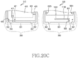
- FIG. 20A to FIG. 20G illustrate an electronic device including an antenna having a single feeding portion including a stub pattern connected with a switching circuit according to an embodiment of the present disclosure
- FIG. 21A and FIG. 21B illustrate an electronic device including an antenna having a single feeding portion including a stub pattern connected with a switching circuit according to another embodiment of the present disclosure
- FIG. 22 is a graph illustrating a radiation efficiency of an electronic device including an antenna according to FIG. 13A to FIG. 21B described above;
- FIG. 23A to FIG. 23D illustrate an electronic device including an antenna according to various embodiments of the present disclosure
- FIG. 24A to FIG. 24D illustrate an electronic device including an antenna according to various embodiments of the present disclosure
- FIG. 25A to FIG. 25H illustrate an electronic device including an antenna according to various embodiments of the present disclosure
- FIG. 26A to FIG. 26H illustrate an electronic device including an antenna according to various embodiments of the present disclosure
- FIG. 27A to FIG. 27C illustrate a slide-type electronic device according to various embodiments of the present disclosure
- FIG. 28A and FIG. 28B illustrate a foldable-type electronic device including a flexible display according to various embodiments of the present disclosure
- FIG. 29A to FIG. 29C illustrate a bendable-type electronic device including a flexible display according to various embodiments of the present disclosure
- FIG. 30A and FIG. 30B illustrate a foldable-type electronic device according to various embodiments of the present disclosure.
- FIG. 31A and FIG. 31B illustrate a detachable-type electronic device according to various embodiments of the present disclosure.
- An expression “have”, “may have”, “include” or “may include” or the like used in the present document is intended to indicate a presence of a corresponding characteristic (e.g., a number, a function, an operation, or a constitutional element such as a component), and should be understood that there are additional possibilities of one or more other characteristics.
- an expression “A or B”, “A and/or B”, or “one or more of A and/or B” or the like may include all possible combinations of items enumerated together.
- “A or B”, “at least one of A and B”, or “at least one of A or B” may indicate all cases where: (1) at least one A is included; (2) at least one B is included; and (3) at least one A and at least one B are both included.
- expressions such as “1 st ”, “2 nd ”, “first”, and “second” may be used in the present document to express various constitutional elements, it is not intended to limit the corresponding constitutional elements.
- the above expressions may be used to distinguish one constitutional element from another constitutional element.
- a 1 st user device and a 2 nd user device are both user devices, and indicate different user devices.
- a 1 st constitutional element may be termed a 2 nd constitutional element, and similarly, the 2 nd constitutional element may be termed the 1 st constitutional element without departing from the scope of the present document.
- a certain constitutional element e.g., the 1 st constitutional element
- a different constitutional element e.g., the 2 nd constitutional element
- the certain constitutional element is directly coupled with/to another constitutional element or can be coupled with/to the different constitutional element via another constitutional element (e.g., a 3 rd constitutional element).
- the certain constitutional element e.g., the 1 st constitutional element
- the different constitutional element e.g., the 2 nd constitutional element
- another constitutional element e.g., the 3 rd constitutional element
- An expression “configured to” used in the present document may be interchangeably used with, for example, “suitable for”, “having the capacity to”, “designed to”, “adapted to”, “made to”, or “capable of” according to a situation.
- a term “configured to” may not imply only “specially designed to” in a hardware manner. Instead, in a certain situation, an expressed “a device configured to” may imply that the device is “capable of” together with other devices or components.
- a processor configured to perform A, B, and C may imply a dedicated processor (e.g., an embedded processor) for performing a corresponding operation or a generic-purpose processor (e.g., Central Processing Unit (CPU) or an application processor) capable of performing corresponding operations by executing one or more software programs stored in a memory device.
- a dedicated processor e.g., an embedded processor
- a generic-purpose processor e.g., Central Processing Unit (CPU) or an application processor
- An electronic device may include, for example, at least one of a smart phone, a tablet Personal Computer (PC), a mobile phone, a video phone, an e-book reader, a desktop PC, a laptop PC, a netbook computer, a workstation, a server, a Personal Digital Assistant (PDA), a Portable Multimedia Player (PMP), a MPEG-1 Audio Layer 3 (MP3) player, a mobile medical device, a camera, and a wearable device.
- a smart phone a tablet Personal Computer (PC)
- PC Personal Computer
- PDA Personal Digital Assistant
- PMP Portable Multimedia Player
- MP3 MPEG-1 Audio Layer 3
- the wearable device may include at least one of an accessory-type device (e.g., a watch, a ring, a bracelet, an anklet, a necklace, glasses, contact lenses, or a Head-Mounted Device (HMD)), a fabric- or clothes-integrated device (e.g., electronic clothes), a body attaching-type device (e.g., a skin pad or tattoo), or a body implantable device (e.g., an implantable circuit).
- an accessory-type device e.g., a watch, a ring, a bracelet, an anklet, a necklace, glasses, contact lenses, or a Head-Mounted Device (HMD)
- a fabric- or clothes-integrated device e.g., electronic clothes
- a body attaching-type device e.g., a skin pad or tattoo
- a body implantable device e.g., an implantable circuit
- the electronic device may be a home appliance.
- the home appliance may include, for example, at least one of a TeleVision (TV), a Digital Video Disk (DVD) player, an audio player, a refrigerator, an air conditioner, a cleaner, an oven, a microwave oven, a washing machine, an air purifier, a set-top box, a home automation control panel, a security control panel, a TV box (e.g., Samsung HomeSyncTM, Apple TVTM, or Google TVTM), a game console (e.g., XboxTM, PlayStationTM), an electronic dictionary, an electronic key, a camcorder, and an electronic picture frame.
- TV TeleVision
- DVD Digital Video Disk
- the electronic device may include at least one of various medical devices (e.g., various portable medical measuring devices (e.g., a blood sugar measuring device, a hear rate measuring device, a blood pressure measuring device, a body temperature measuring device, etc.), Magnetic Resonance Angiography (MRA), Magnetic Resonance Imaging (MM), Computed Tomography (CT), imaging equipment, ultrasonic instrument, etc.)), a navigation device, a Global Positioning System (GPS) receiver, an Event Data Recorder (EDR), a Flight Data Recorder (FDR), a car infotainment device, an electronic equipment for ship (e.g., a vessel navigation device, a gyro compass, etc.), avionics, a security device, a car head unit, an industrial or domestic robot, an Automatic Teller's Machine (ATM) of financial institutions, Point Of Sales (POS) of shops, and Internet of things (e.g., a light bulb, various sensors, an electric or gas meter, etc.
- ATM
- the electronic device may include at least one of furniture or a part of buildings/constructions, an electronic board, an electronic signature input device, a projector, and various measurement machines (e.g., water supply, electricity, gas, propagation measurement machine, etc.).
- the electronic device may be one or more combinations of the aforementioned various devices.
- the electronic device may be a flexible device.
- the electronic device according to one exemplary embodiment of the present document is not limited to the aforementioned devices, and may include a new electronic device depending on technical progress.
- the term “user” used in the present document may refer to a person who uses the electronic device or a device which uses the electronic device (e.g., an Artificial Intelligence (AI) electronic device).
- AI Artificial Intelligence
- FIG. 1 illustrates a network environment including an electronic device according to various embodiments.
- the electronic device 101 may include a bus 110 , a processor 120 , a memory 130 , an input/output interface 150 , a display 160 , and a communication interface 170 .
- the electronic device 101 may omit at least one of the aforementioned constitutional elements or may additionally include other constitutional elements.
- the bus 110 may include a circuit for connecting the aforementioned constitutional elements 120 to 170 to each other and for delivering communication (e.g., a control message and/or data) between the aforementioned constitutional elements.
- the processor 120 may include one or more of a Central Processing Unit (CPU), an Application Processor (AP), and a Communication Processor (CP).
- the processor 120 may control, for example, at least one of other constitutional elements of the electronic device 101 and/or may execute an arithmetic operation or data processing for communication.
- the memory 130 may include a volatile and/or non-volatile memory.
- the memory 130 may store, for example, an instruction or data related to at least one different constitutional element of the electronic device 101 .
- the memory 130 may store a software and/or a program 140 .
- the program 140 may include, for example, a kernel 141 , a middleware 143 , an Application Programming Interface (API) 145 , and/or an application program (or an “application”) 147 , or the like.
- API Application Programming Interface
- At least one part of the kernel 141 , middleware 143 , or API 145 may be referred to as an Operating System (OS).
- OS Operating System
- the kernel 141 may control or manage, for example, system resources (e.g., the bus 110 , the processor 120 , the memory 130 , etc.) used to execute an operation or function implemented in other programs (e.g., the middleware 143 , the API 145 , or the application program 147 ). Further, the kernel 141 may provide an interface capable of controlling or managing the system resources by accessing individual constitutional elements of the electronic device 101 in the middleware 143 , the API 145 , or the application program 147 .
- system resources e.g., the bus 110 , the processor 120 , the memory 130 , etc.
- the kernel 141 may provide an interface capable of controlling or managing the system resources by accessing individual constitutional elements of the electronic device 101 in the middleware 143 , the API 145 , or the application program 147 .
- the middleware 143 may perform, for example, a mediation role so that the API 145 or the application program 147 can communicate with the kernel 141 to exchange data.
- the middleware 143 may handle one or more task requests received from the application program 147 according to a priority. For example, the middleware 143 may assign a priority of using the system resources (e.g., the bus 110 , the processor 120 , or the memory 130 ) of the electronic device 101 to at least one of the application programs 147 . For instance, the middleware 143 may process the one or more task requests according to the priority assigned to the at least one of the application programs, and thus may perform scheduling or load balancing on the one or more task requests.
- system resources e.g., the bus 110 , the processor 120 , or the memory 130
- the API 145 may include at least one interface or function (e.g., instruction), for example, for file control, window control, video processing, or character control, as an interface capable of controlling a function provided by the application 147 in the kernel 141 or the middleware 143 .
- interface or function e.g., instruction
- the input/output interface 150 may play a role of an interface for delivering an instruction or data input from a user or a different external device(s) to the different constitutional elements of the electronic device 101 . Further, the input/output interface 150 may output an instruction or data received from the different constitutional element(s) of the electronic device 101 to the different external device.
- the display 160 may include various types of displays, for example, a Liquid Crystal Display (LCD) display, a Light Emitting Diode (LED) display, an Organic Light-Emitting Diode (OLED) display, a MicroElectroMechanical Systems (MEMS) display, or an electronic paper display.
- the display 160 may display, for example, a variety of contents (e.g., text, image, video, icon, symbol, etc.) to the user.
- the display 160 may include a touch screen.
- the display 160 may receive a touch, gesture, proximity, or hovering input by using a stylus pen or a part of a user's body.
- the communication interface 170 may establish, for example, communication between the electronic device 101 and the external device (e.g., a 1 st external electronic device 102 , a 2 nd external electronic device 104 , or a server 106 ).
- the communication interface 170 may communicate with the external device (e.g., the 2 nd external electronic device 104 or the server 106 ) by being connected with a network 162 through wireless communication or wired communication.
- the wireless communication may use at least one of Long-Term Evolution (LTE), LTE Advance (LTE-A), Code Division Multiple Access (CDMA), Wideband CDMA (WCDMA), Universal Mobile Telecommunications System (UMTS), Wireless Broadband (WiBro), Global System for Mobile Communications (GSM), and the like.
- LTE Long-Term Evolution
- LTE-A LTE Advance
- CDMA Code Division Multiple Access
- WCDMA Wideband CDMA
- UMTS Universal Mobile Telecommunications System
- WiBro Wireless Broadband
- GSM Global System for Mobile Communications
- the wireless communication may include, for example, a near-distance communication 164 .
- the near-distance communication 164 may include, for example, at least one of Wireless Fidelity (WiFi), Bluetooth, Near Field Communication (NFC), Global Navigation Satellite System (GNSS), and the like.
- WiFi Wireless Fidelity
- NFC Near Field Communication
- GNSS Global Navigation Satellite System
- the GNSS may include, for example, at least one of Global Positioning System (GPS), Global Navigation Satellite System (Glonass), Beidou Navigation Satellite System (hereinafter, “Beidou”), Galileo, the European global satellite-based navigation system, and the like.
- GPS Global Positioning System
- Glonass Global Navigation Satellite System
- Beidou Beidou Navigation Satellite System
- Galileo the European global satellite-based navigation system
- the wired communication may include, for example, at least one of Universal Serial Bus (USB), High Definition Multimedia Interface (HDMI), Recommended Standard-232 (RS-232), power-line communication, Plain Old Telephone Service (POTS), and the like.
- the network 162 may include, for example, at least one of a telecommunications network, a computer network (e.g., LAN or WAN), the Internet, and a telephone network.
- Each of the 1 st and 2 nd external electronic devices 102 and 104 may be the same type or different type of the electronic device 101 .
- the server 106 may include a group of one or more servers. According to various exemplary embodiments, all or some of operations executed by the electronic device 101 may be executed in a different one or a plurality of electronic devices (e.g., the electronic device 102 or 104 or the server 106 ).
- the electronic device 101 may request at least a part of functions related thereto alternatively or additionally to a different electronic device (e.g., the electronic device 102 or 104 or the server 106 ) instead of executing the function or the service autonomously.
- the different electronic device e.g., the electronic device 102 or 104 or the server 106
- the electronic device 101 may provide the requested function or service either directly or by additionally processing the received result.
- a cloud computing, distributed computing, or client-server computing technique may be used.
- a conductive member used for an antenna radiator may include a conductive member disposed around edge of the electronic device as examples, but the conductive member used for an antenna radiator is not limited thereto.
- various structures comprising metal material may be used for an antenna radiator.
- the electronic device may be a bar-type electronic device, but the electronic device in not limited thereto.
- the electronic device may be an electronic device with various open and close types, or may be a wearable electronic device.
- FIG. 2 is a block diagram of an electronic device according to various exemplary embodiments.
- the electronic device 201 may include, for example, all or some parts of the electronic device 101 of FIG. 1 .
- the electronic device 201 may include one or more processors (e.g., Application Processors (APs)) 210 , a communication module 220 , a subscriber identity module 224 , a memory 230 , a sensor module 240 , an input unit 250 , a display 260 , an interface 270 , an audio module 280 , a camera module 291 , a power management module 295 , a battery 296 , an indicator 297 , and a motor 298 .
- APs Application Processors
- the processor 210 may control a plurality of hardware or software constitutional elements connected to the processor 210 by driving, for example, an operating system or an application program, and may process a variety of data including multimedia data and may perform an arithmetic operation.
- the processor 210 may be implemented, for example, with a System on Chip (SoC).
- SoC System on Chip
- the processor 210 may further include a Graphic Processing Unit (GPU) and/or an image signal processor.
- the processor 210 may include at least one part (e.g., a cellular module 221 ) of the aforementioned constitutional elements of FIG. 2 .
- the processor 210 may process an instruction or data, which is received from at least one of different constitutional elements (e.g., a non-volatile memory), by loading it to a volatile memory and may store a variety of data in the non-volatile memory.
- the communication module 220 may have the same or similar configuration of the communication interface 170 of FIG. 1 .
- the communication module 220 may include, for example, the cellular module 221 , a Wi-Fi module 223 , a BlueTooth (BT) module 225 , a GNSS module 227 (e.g., a GPS module, a Glonass module, a Beidou module, or a Galileo module), a Near Field Communication (NFC) module 228 , and a Radio Frequency (RF) module 229 .
- BT BlueTooth
- GNSS e.g., a GPS module, a Glonass module, a Beidou module, or a Galileo module
- NFC Near Field Communication
- RF Radio Frequency
- the cellular module 221 may provide a voice call, a video call, a text service, an Internet service, or the like, for example, through a communication network.
- the cellular module 221 may identify and authenticate the electronic device 201 in the communication network by using the subscriber identity module (e.g., a Subscriber Identity Module (SIM) card) 224 .
- the cellular module 221 may perform at least some functions that can be provided by the processor 210 .
- the cellular module 221 may include a Communication Processor (CP).
- CP Communication Processor
- Each of the WiFi module 223 , the Bluetooth module 225 , the GNSS module 227 , and the NFC module 228 may include, for example, a processor for processing data transmitted/received through a corresponding module.
- a processor for processing data transmitted/received through a corresponding module may be included in one Integrated Chip (IC) or IC package.
- IC Integrated Chip
- the RF module 229 may transmit/receive, for example, a communication signal (e.g., a Radio Frequency (RF) signal).
- the RF module 229 may include, for example, a transceiver, a Power Amp Module (PAM), a frequency filter, a Low Noise Amplifier (LNA), an antenna, or the like.
- PAM Power Amp Module
- LNA Low Noise Amplifier
- at least one of the cellular module 221 , the WiFi module 223 , the BT module 225 , the GPS module 227 , and the NFC module 228 may transmit/receive an RF signal via a separate RF module.
- the subscriber identity module 224 may include, for example, a card including the subscriber identity module and/or an embedded SIM, and may include unique identification information (e.g., an Integrated Circuit Card IDentifier (ICCID)) or subscriber information (e.g., an International Mobile Subscriber Identity (IMSI)).
- ICCID Integrated Circuit Card IDentifier
- IMSI International Mobile Subscriber Identity
- the memory 230 may include, for example, an internal memory 232 or an external memory 234 .
- the internal memory 232 may include, for example, at least one of a volatile memory (e.g., a Dynamic RANI (DRAM), a Static RAM (SRAM), a Synchronous Dynamic RAM (SDRAM), etc.) and a non-volatile memory (e.g., a One Time Programmable ROM (OTPROM), a Programmable ROM (PROM), an Erasable and Programmable ROM (EPROM), an Electrically Erasable and Programmable ROM (EEPROM), a mask ROM, a flash ROM, a flash memory (e.g., a NAND flash memory, a NOR flash memory, etc.), a hard drive, or a Solid State Drive (SSD)).
- a volatile memory e.g., a Dynamic RANI (DRAM), a Static RAM (SRAM), a Synchronous Dynamic RAM (SDRAM), etc.
- the external memory 234 may further include a flash drive, for example, Compact Flash (CF), Secure Digital (SD), Micro Secure Digital (Micro-SD), Mini Secure digital (Mini-SD), extreme Digital (xD), memory stick, or the like.
- CF Compact Flash
- SD Secure Digital
- Micro-SD Micro Secure Digital
- Mini-SD Mini Secure digital
- xD extreme Digital
- the external memory 234 may be operatively and/or electrically connected to the electronic device 201 via various interfaces.
- the sensor module 240 may measure, for example, physical quantity or detect an operational status of the electronic device 201 , and may convert the measured or detected information into an electric signal.
- the sensor module 240 may include, for example, at least one of a gesture sensor 240 A, a gyro sensor 240 B, a pressure sensor 240 C, a magnetic sensor 240 D, an acceleration sensor 240 E, a grip sensor 240 F, a proximity sensor 240 G, a color sensor 240 H (e.g., a Red, Green, Blue (RGB) sensor), a bio sensor 240 I, a temperature/humidity sensor 240 J, an illumination sensor 240 K, and an Ultra Violet (UV) sensor 240 M, an ultrasonic sensor 240 N.
- a gesture sensor 240 A e.g., a gyro sensor 240 B
- a pressure sensor 240 C e.g., a pressure sensor 240 C
- a magnetic sensor 240 D e.g.,
- the sensor module 240 may include, for example, an E-nose sensor, an ElectroMyoGraphy (EMG) sensor, an ElectroEncephaloGram (EEG) sensor, an ElectroCardioGram (ECG) sensor, an Infrared (IR) sensor, an iris sensor, and/or a fingerprint sensor.
- the sensor module 240 may further include a control circuit for controlling at least one or more sensors included therein.
- the electronic device 201 may further include a processor configured to control the sensor module 204 either separately or as one part of the processor 210 , and may control the sensor module 240 while the processor 210 is in a sleep state.
- the input unit 250 may include, for example, a touch panel 252 , a (digital) pen sensor 254 , a key 256 , or an ultrasonic input device 258 .
- the touch panel 252 may recognize a touch input, for example, by using at least one of an electrostatic type, a pressure-sensitive type, and an ultrasonic type.
- the touch panel 252 may further include a control circuit.
- the touch penal 252 may further include a tactile layer and thus may provide the user with a tactile reaction.
- the (digital) pen sensor 254 may be, for example, one part of a touch panel, or may include an additional sheet for recognition.
- the key 256 may be, for example, a physical button, an optical key, a keypad, or a touch key.
- the ultrasonic input device 258 may detect an ultrasonic wave generated from an input means through a microphone (e.g., a microphone 288 ) to confirm data corresponding to the detected ultrasonic wave.
- the display 260 may include a panel 262 , a hologram unit 264 , or a projector 266 .
- the panel 262 may include the same or similar structure of the display 160 of FIG. 1 .
- the panel 262 may be implemented, for example, in a flexible, transparent, or wearable manner.
- the panel 262 may be constructed as one module with the touch panel 252 .
- the hologram unit 264 may use an interference of light and show a stereoscopic image in the air.
- the projector 266 may display an image by projecting a light beam onto a screen.
- the screen may be located, for example, inside or outside the electronic device 201 .
- the display 260 may further include a control circuit for controlling the panel 262 , the hologram unit 264 , or the projector 266 .
- the interface 270 may include, for example, a High-Definition Multimedia Interface (HDMI) 272 , a Universal Serial Bus (USB) 274 , an optical communication interface 276 , or a D-subminiature (D-sub) 278 .
- the interface 270 may be included, for example, in the communication interface 170 of FIG. 1 .
- the interface 270 may include, for example, a Mobile High-definition Link (MHL) interface, a Secure Digital (SD)/Multi-Media Card (MMC) interface, or an Infrared Data Association (IrDA) standard interface.
- MHL Mobile High-definition Link
- SD Secure Digital
- MMC Multi-Media Card
- IrDA Infrared Data Association
- the audio module 280 may bilaterally convert, for example, a sound and electric signal. At least some constitutional elements of the audio module 280 may be included in, for example, the input/output interface 150 of FIG. 1 .
- the audio module 280 may convert sound information which is input or output, for example, through a speaker 282 , a receiver 284 , an earphone 286 , the microphone 288 , or the like.
- the camera module 291 is, for example, a device for image and video capturing, and according to one exemplary embodiment, may include one or more image sensors (e.g., a front sensor or a rear sensor), a lens, an Image Signal Processor (ISP), or a flash (e.g., LED or xenon lamp).
- image sensors e.g., a front sensor or a rear sensor
- lens e.g., a lens
- ISP Image Signal Processor
- flash e.g., LED or xenon lamp
- the power management module 295 may manage, for example, power of the electronic device 201 .
- the power management module 295 may include a Power Management Integrated Circuit (PMIC), a charger Integrated Circuit (IC), or a battery fuel gauge.
- the PMIC may have a wired and/or wireless charging type.
- the wireless charging type may include, for example, a magnetic resonance type, a magnetic induction type, an electromagnetic type, or the like, and may further include an additional circuit for wireless charging, for example, a coil loop, a resonant circuit, a rectifier, or the like.
- the battery gauge may measure, for example, residual quantity of the battery 296 and voltage, current, and temperature during charging.
- the battery 296 may include, for example, a rechargeable battery and/or a solar battery.
- the indicator 297 may display a specific state, for example, a booting state, a message state, a charging state, or the like, of the electronic device 201 or one part thereof (e.g., the processor 210 ).
- the motor 298 may convert an electric signal into a mechanical vibration, and may generate a vibration or haptic effect.
- the electronic device 201 may include a processing unit (e.g., a GPU) for supporting a mobile TV.
- the processing unit for supporting the mobile TV may process media data according to a protocol of, for example, Digital Multimedia Broadcasting (DMB), Digital Video Broadcasting (DVB), MediaFloTM, or the like.
- DMB Digital Multimedia Broadcasting
- DVD Digital Video Broadcasting
- MediaFloTM MediaFloTM
- Each of constitutional elements described in the present document may consist of one or more components, and names thereof may vary depending on a type of an electronic device.
- the electronic device according to various exemplary embodiments may include at least one of the constitutional elements described in the present document. Some of the constitutional elements may be omitted, or additional other constitutional elements may be further included. Further, some of the constitutional elements of the electronic device according to various exemplary embodiments may be combined and constructed as one entity, so as to equally perform functions of corresponding constitutional elements before combination.
- an electronic device including an antenna may be an electronic device having various rotation mechanisms including a first housing and a second housing rotatably disposed to the first housing, but the electronic device is not limited thereto.
- the present disclosure may also apply to an electronic device having a single housing to which an antenna is disposed and a conductive member (e.g., a metal member, a metal ornament, etc.) is also disposed in a region overlapping with the antenna.
- FIG. 3A to FIG. 3C are a perspective view and lateral view of an electronic device according to various embodiments of the present disclosure.
- FIG. 3D is a drawing for briefly explaining an outer side of an electronic device according to various embodiments of the present disclosure.
- An X-axis may represent a lengthwise direction (e.g., a long-side direction) of an electronic device 300
- a Y-axis may represent a widthwise direction (e.g., a short-side direction) of the electronic device 300
- a Z-axis may represent an up-and-down direction of the electronic device 300 .
- the electronic device 300 may include a first housing 310 , a second housing 320 , and a connecting member 330 for connecting the first housing 310 and the second housing 320 .
- the first housing 310 and the second housing 320 may constitute the entirety or part of an exterior of the electronic device 300 .
- the first housing 310 and/or the second housing 320 may be constructed of various materials.
- the first housing 310 and/or the second housing 320 may be constructed of materials such as plastics, metals, carbon fibers and other fiber composites, ceramics, glass, wood, or combinations of these materials.
- the first housing 310 may include a first side 341 facing a first direction z, a second side 342 facing a second direction ⁇ z opposite to the first direction 341 , and a first lateral side 343 at least partially surrounding a space between the first side 341 and the second side 342 .
- the first housing 310 may have a substantially rectangular plate shape.
- the first side 341 may have a substantially rectangular shape including a first edge # 1 341 - 1 , a first edge # 2 341 - 2 , a first edge # 3 341 - 3 , and a first edge # 4 341 - 4 .
- the first edge # 1 341 - 1 and the first edge # 2 341 - 2 may be disposed at opposite sides, and the first edge # 3 341 - 3 and the first edge # 4 341 - 4 may be disposed at opposite sides.
- the first edge # 1 341 - 1 may connect one end of the first edge # 3 341 - 3 and one end of the first edge # 4 341 - 4 .
- the first edge # 2 341 - 2 may connect the other end of the first edge # 3 341 - 3 and the other end of the first edge # 4 341 - 4 .
- the second side 342 may have a substantially rectangular shape including a second edge # 1 342 - 1 , a second edge # 2 342 - 2 , a second edge # 3 342 - 3 , and a second edge # 4 342 - 4 .
- the second edge # 1 342 - 1 and the second edge # 2 342 - 2 may be disposed at opposite sides, and the second edge # 3 342 - 3 and the second edge # 4 342 - 4 may be disposed at opposite sides.
- the second edge # 1 342 - 1 may connect one end of the second edge # 3 342 - 3 and one end of the second edge # 4 342 - 4 .
- the second edge # 2 342 - 2 may connect the other end of the second edge # 3 342 - 3 and the other end of the second edge # 4 342 - 4 .
- the first lateral side 343 may have a substantially rectangular annular shape including the first lateral side # 1 343 - 1 , the first lateral side # 2 343 - 2 , the first lateral side # 3 343 - 3 , and the first lateral side # 4 343 - 4 .
- the first lateral side # 1 343 - 1 and the first lateral side # 2 343 - 2 may be disposed at opposite sides.
- the first lateral side # 3 343 - 3 and the first lateral side # 4 343 - 4 may be disposed at opposite sides.
- the first lateral side # 1 343 - 1 may connect the first edge # 1 341 - 1 of the first side 341 and the second edge # 1 342 - 1 of the second side 342 .
- the first lateral side # 2 343 - 2 may connect the first edge # 2 341 - 2 of the first side 341 and the second edge # 2 342 - 2 of the second side 342 .
- the first lateral side # 3 343 - 3 may connect the first edge # 3 341 - 3 of the first side 341 and the second edge # 3 342 - 3 of the second side 342 .
- the first lateral side # 4 343 - 4 may connect the first edge # 4 341 - 4 of the first side 341 and the second edge # 4 342 - 4 of the second side 342 .
- the electronic device 300 may include various shapes of electronic components disposed to abut against the first side 341 of the first housing 310 .
- the electronic component may include a first display 311 disposed along at least part of the first side 341 of the first housing 310 .
- the first display 311 may be exposed through the first side 341 of the first housing 310 .
- the first display 311 may further include a panel capable of receiving a touch input or a hovering input.
- the first display 311 may further include a panel (e.g., a digitizer) capable of receiving the touch input or the hovering input by using a stylus.
- the first display 311 may include various shapes of touch screens.
- the first display 311 may have a shape in which sensors for the touch input or the hovering input are combined with an on-cell region or in-cell region of the display panel.
- the first display 311 may have a substantially rectangular shape including four edges.
- the first display 311 may include a screen first edge # 1 311 - 1 abutting against the first edge # 1 341 - 1 of the first side 341 , a screen first edge # 2 311 - 2 abutting against the first edge # 2 341 - 1 of the first side 341 , a screen first edge # 3 311 - 3 abutting against the first edge # 3 341 - 3 of the first side 341 , and a screen first edge # 4 311 - 4 abutting against the first edge # 4 341 - 4 of the first side 341 .
- the electronic device 300 may output a main home screen by using the first display 311 .
- the main home screen may be a first screen displayed on the display 311 when power of the electronic device 300 is on.
- the main home screen may be a first home screen among the several pages of the home screens.
- Short-cut icons, a main menu switching key, time, weather, or the like may be displayed on the home screen to execute frequently used applications.
- the main menu switching key may display a menu screen on the display 311 .
- a status bar indicating a status of the electronic device 300 such as a battery charging status, received signal strength, and current time, may be displayed on an upper region included in the display 311 .
- the electronic device 300 may include various shapes of electronic components disposed between the first edge # 1 341 - 1 of the first side 341 and the screen first edge # 1 311 - 1 of the first display 311 .
- the electronic component may include a receiver 312 to output a voice transmitted from a peer terminal during a call is made.
- the electronic component may include at least one of sensors 313 , 314 , and 135 .
- the sensors 313 , 314 , and 315 may include at least one of, for example, an illumination sensor (e.g., an optical sensor), a proximity sensor (e.g., an optical sensor), an infrared sensor, and an ultrasonic sensor.
- the electronic component may include a camera 316 (or a front camera).
- the electronic device 300 may include various shapes of electronic components disposed between the first edge # 2 341 - 2 of the first side 341 and the first edge # 2 311 - 2 of the first display 311 .
- the electronic component may be a touch key, a key button, or the like.
- the key button may perform a home key button function.
- a fingerprint sensor device may be disposed to the home key button.
- a signal may be generated by a gesture which physically presses the home key button, and the electronic device 300 may perform a first function (a home screen return function, a wake-up/sleep function, etc.) based on this signal.
- a signal may be generated by a gesture which swipes or touches an upper side of the home key button, and the electronic device 300 may perform a second function (e.g., a fingerprint recognition function, etc.) based on this signal.
- the electronic device 300 may include various shapes of electronic components disposed to abut against the second side 342 of the first housing 310 .
- the electronic component may include a camera (or a rear camera), a camera flash, a speaker, an output device (e.g., a button), or the like.
- the electronic component may include a display (not shown).
- the electronic device 300 may include various shapes of electronic components disposed to abut against the first lateral side 343 of the first housing 341 .
- the electronic component may include a socket device (not shown) capable of connecting a card-type external device.
- the electronic component may include a socket device (not shown) capable of connecting a memory card (e.g., Compact Flash (CF), Multi Media Card (MMC), Smart Media Card (SMC), a Secure Disk (SD), a Memory Stick (MS), etc.).
- the electronic component may include a socket device (not shown) capable of connecting a Subscriber Identification Module (SIM) card or a Universal Subscriber Identification Module (ISIM) card.
- the electronic component may include an interface connector port 317 .
- the interface connector port 317 may be used to charge the electronic device 300 by using a data transmission/reception function and/or external power provided by an external device.
- the electronic component may include a socket device (e.g., an ear jack) (not shown) capable of inserting an ear plug.
- the first lateral side 343 may include a through-hole for various shapes of the socket device.
- the interface connector port 317 may be disposed to the first lateral side # 2 343 - 2 of the first housing 341 , and the ear jack may be disposed to the first lateral side # 1 343 - 1 of the first housing 341 .
- the electronic device 300 may include various shapes of key buttons (or side key buttons) disposed to the first lateral side 343 of the first housing 310 .
- key buttons or side key buttons
- at least one key button may be disposed to the first lateral side # 3 343 - 3 , and may be used for a volume up/down function, a scroll function, or the like.
- Another key button of the at least one key button may be disposed to the first lateral side # 4 343 - 4 , and may be used for a power on/off function, a wake-up/sleep function of the electronic device, or the like.
- the second housing 320 may include a third side 346 facing a third direction z, a fourth side 347 facing a fourth direction ⁇ z opposite to the third direction z, and a second lateral side 348 at least partially surrounding a space between the third side 346 and the fourth side 347 .
- the second housing 320 may have a substantially rectangular plate shape.
- the third side 346 may have a substantially rectangular shape including a third edge # 1 346 - 1 , a third edge # 2 346 - 2 , a third edge # 3 346 - 3 , and a third edge # 4 346 - 4 .
- the third edge # 1 346 - 1 and the third edge # 2 346 - 2 may be disposed at opposite sides, and the third edge # 3 346 - 3 and the third edge # 4 346 - 4 may be disposed at opposite sides.
- the third edge # 1 346 - 1 may connect one end of the third edge # 3 346 - 3 and one end of the third edge # 4 346 - 4 .
- the third edge # 2 346 - 2 may connect the other end of the third edge # 3 346 - 3 and the other end of the third edge # 4 346 - 4 .
- the fourth side 347 may have a substantially rectangular shape including a fourth edge # 1 347 - 1 , a fourth edge # 2 347 - 2 , a fourth edge # 3 347 - 3 , and a fourth edge # 4 347 - 4 .
- the fourth edge # 1 347 - 1 and the fourth edge # 2 347 - 2 may be disposed at opposite sides, and the fourth edge # 3 347 - 3 and the fourth edge # 4 347 - 4 may be disposed at opposite sides.
- the fourth edge # 1 347 - 1 may connect one end of the fourth edge # 3 347 - 3 and one end of the fourth edge # 4 347 - 4 .
- the fourth edge # 2 347 - 2 may connect the other end of the fourth edge # 3 347 - 3 and the other end of the fourth edge # 4 347 - 4 .
- the second lateral side 348 may have a substantially rectangular annular shape including a second lateral side # 1 348 - 1 , a second lateral side # 2 348 - 2 , a second lateral side # 3 348 - 3 , and a second lateral side # 4 348 - 4 .
- the second lateral side # 1 348 - 1 and the second lateral side # 2 348 - 2 may be disposed at opposite sides.
- the second lateral side # 3 348 - 3 and the second lateral side # 4 348 - 4 may be disposed at opposite sides.
- the second lateral side # 1 348 - 1 may connect the second edge # 1 341 - 1 of the third side 346 and the second edge # 1 342 - 1 of the fourth side 347 .
- the second lateral side # 2 348 - 2 may connect the second edge # 2 341 - 2 of the third side 346 and the second edge # 2 342 - 2 of the fourth side 347 .
- the second lateral side # 3 348 - 3 may connect the third edge # 3 346 - 3 of the third side 346 and the fourth edge # 3 347 - 3 of the fourth side 347 .
- the second lateral side # 4 348 - 4 may connect the third edge # 4 346 - 4 of the third side 346 and the fourth edge # 4 347 - 4 of the fourth side 347 .
- the electronic device 300 may include various shapes of electronic components disposed to abut against the third side 346 of the second housing 320 .
- the electronic component may include a second display 321 disposed along at least part of the third side 346 of the second housing 320 .
- the second display 321 may be exposed through the third side 346 of the second housing 320 .
- the second display 321 may further include a panel capable of receiving a touch input or a hovering input.
- the second display 321 may further include a panel (e.g., a digitizer) capable of receiving the touch input or the hovering input by using a stylus.
- the second display 321 may include various shapes of touch screens.
- the first display 311 may have a shape in which sensors for the touch input or the hovering input are combined with an on-cell region or in-cell region of the display panel.
- the electronic device 300 may include various shapes of electronic components (e.g., a display sensor, a speaker, a socket, etc.) (not shown) disposed to abut against the fourth lateral side 347 of the second housing 320 .
- the electronic device 300 may include various shapes of electronic components (e.g., key buttons) (not shown) disposed to the second lateral side 348 of the second housing 320 .
- the first display 311 may include a substantially flat surface.
- at least part of the first display 311 may include a curved portion having a curvature.
- the curved portion may be constructed to have an inclined or curved side.
- the first display 311 may include a first edge region # 3 (not shown) abutting against the screen first edge # 3 311 - 3 and a first edge region # 4 (not shown) abutting against the first edge # 3 311 - 4 .
- the first display 311 may include a central region (not shown) disposed between the first edge region # 3 and the first edge region # 4 .
- At least one of the first edge region # 3 and the first edge region # 4 may include an inclined or curved side which is bent in a direction from the first side 341 to second side 342 of the first housing 310 .
- the central region may include a substantially flat plane.
- the second display 321 may include a substantially flat surface. Alternatively, at least part of the second display 321 may include an inclined or curved side.
- the electronic device 300 may control a display module to selectively display at least part of information by using at least part of at least one of the first display 311 and the second display 321 .
- the connecting member 330 may connect the first housing 310 and the second housing 320 .
- the second housing 320 may rotate about the first housing 310 by using the connecting member 330 .
- the first housing 310 may rotate about the second housing 320 by using the connecting member 330 .
- the second housing 320 may rotate to cover the first side 341 of the first housing 310 .
- the second housing 320 may rotate to cover the second side 342 of the first housing 310 .
- the connecting member 330 may establish a connection between the first lateral side # 4 343 - 4 of the first housing 310 and the second lateral side # 3 348 - 3 of the second housing 320 .
- the connecting member 330 may be constructed in various shapes.
- the connecting member 330 may be constructed as a hinge unit.
- the connecting member 330 may include at least one hinge arm.
- a well-known hinge module e.g., a hinge cam, a hinge shaft, a hinge spring, etc. may be disposed in the hinge arm.
- the connecting member 330 may be constructed as a polymer member.
- the connecting member 330 may be constructed of leathers, artificial leathers, plastic materials, metallic materials, or fiber materials, or may be constructed of a plurality of polymer layers.
- the connecting member 330 may include various shapes of flexible members.
- the electronic device 300 may have at least three shapes as shown in FIG. 3A to FIG. 3C , depending on a rotation angle of the second housing 320 .
- FIG. 3A illustrates an unfolded state (or an open mode state) of the electronic device 300 .
- FIG. 3B illustrates a first folded state of the electronic device 300 .
- the first folded state may represent a state in which the second housing 320 rotates about an axis A 1 as a rotation axis to cover the first side 341 of the first housing 310 .
- the first display 311 of the first housing 310 and the second display 321 of the second housing 320 may face each other, and may not be exposed.
- FIG. 3C illustrates a second folded state of the electronic device 300 .
- the third folded state may represent a state in which the second housing 320 rotates about an axis A 1 as a rotation axis to cover the third side 343 of the first housing 310 .
- the first display 311 of the first housing 310 and the second display 321 of the second housing 320 may be exposed in opposite directions.
- the connecting member 330 may connect the first housing 310 and the second housing 320 such that the first side 341 of the first housing 310 and the third side 346 of the second housing 320 are folded towards each other (or to face each other).
- the connecting member 330 may connect the first housing 310 and the second housing 320 such that the second side 342 of the first housing 310 and the fourth side 347 of the second housing 320 are folded towards each other (or to face each other).
- the first lateral side 343 of the first housing 310 and the second lateral side 348 of the second housing 320 may abut against each other.
- it may mean that the first lateral side 343 and the second lateral side 348 are in contact or are almost in contact with a slight gap (e.g., within 10 mm).
- a first conductive member 350 may be disposed to at least part of the first lateral side 343 of the first housing 310 .
- the first conductive member 350 may constitute at least part of at least one of the first lateral side # 1 343 - 2 , the first lateral side # 2 343 - 1 , the first lateral side # 3 343 - 3 , and the first lateral side # 4 343 - 4 .
- the first conductive member 350 may include a first non-conductive slit 356 and second non-conductive slit 357 extended in a first direction z or second direction ⁇ z of the first housing 310 so as to be divided into a plurality of conductive segments 351 , 352 , and 353 .
- the non-conductive slits 356 and 357 may be extended from a non-conductive member (e.g., a bracket, etc.) disposed outside or inside the first housing 310 .
- a non-conductive member e.g., a bracket, etc.
- a second conductive member 360 may be disposed to at least part of the second lateral side 348 of the second housing 320 .
- the second conductive member 360 may be disposed to a lower or upper end of the second housing 320 , and may include at least part of both sides of the second housing 320 .
- the second conductive member 360 may include a third non-conductive slit 366 and fourth non-conductive slit 367 extended in a third direction z or fourth direction ⁇ z of the second housing 320 so as to be divided in the plurality of conductive segments 361 , 362 , and 363 .
- the first slit 356 and the fourth slit 367 may abut against each other, and the second list 357 and the third slit 366 may abut against each other.
- the non-conductive slits 356 , 357 , 366 , and 367 may be referred to as a gap, and the non-conductive slits 356 , 357 , 366 , and 367 may be filled with a non-conductive member (e.g., an insulator).
- a non-conductive member e.g., an insulator
- the plurality of conductive segments 351 , 352 , 353 , 361 , 362 , and 363 may include a metallic material.
- the metallic material may include, for example, any one of aluminum, stainless, and an amorphous metal alloy.
- the amorphous metal alloy may have a microstructure similar to a liquid state which does not have a crystal structure since atoms are irregularly arranged.
- the amorphous metal alloy may have uniform isotropic properties, may have excellent mechanical strength due to absence of crystallographic anisotropy, and may have excellent corrosion resistance due to uniform structure and composition.
- an electronic device including an antenna having a plurality of feeding portions (2) an electronic device including an antenna having a switching circuit, (3) an electronic device including an antenna having a stub pattern, and (4) various examples of an electronic device are described distinctively. However, without being limited to embodiments based on such a distinction, the respective embodiments can be applied in a combined or united manner.
- an upper portion ⁇ circle around (1) ⁇ or lower portion ⁇ circle around (2) ⁇ of the first housing 310 of the device 300 or an upper portion ⁇ circle around (3) ⁇ or lower portion ⁇ circle around (4) ⁇ of the second housing 320 may include at least part of at least one of electronic devices including antennas proposed in FIG. 4 , FIG. 5 , FIGS. 6A to 6C , FIGS. 7A to 7C , FIGS. 8A to 8C , FIGS. 9A to 9C , FIGS. 10A to 10C , FIGS. 11A to 11C , FIGS. 13A to 13D , FIGS. 14A to 14D , FIGS. 15A and 15B , FIGS.
- An Electronic Device Including an Antenna having a Plurality of Feeding Portions
- FIG. 4 and FIG. 5 illustrate an electronic device including an antenna having a plurality of feeding portions according to an embodiment of the present disclosure.
- an electronic device including an antenna of the first housing 310 of the electronic device 300 is illustrated in the left side, and an electronic device including an antenna of the second housing 320 of the electronic device 300 is illustrated in the right side.
- the first conductive member 350 disposed to a lower end of the first lateral side 343 of the first housing 310 may be divided into the plurality of conductive segments 351 , 352 , and 353 by the first non-conductive slit 356 and the second non-conductive slit 357 .
- the second conductive segment 352 and/or the third conductive segment 353 may include a substantially ‘L’ shape.
- the first conductive segment 351 may have a substantially linear shape extended to the vicinity of one end portion of the third conductive segment 353 from the vicinity of one end portion of the second conductive segment 352 .
- the second conductive segment 352 and the third conductive segment 353 may have a substantially symmetrical shape.
- the second conductive member 360 disposed to a lower end of the second lateral side 348 of the second housing 320 may be divided into a plurality of conductive segments 361 , 362 , and 363 by the third non-conductive slit 366 and the fourth non-conductive slit 367 .
- the fifth conductive segment 362 and/or the sixth conductive segment 363 may include a substantially ‘L’ shape.
- the fourth conductive segment 361 may have a substantially linear shape extended to the vicinity of one end portion of the sixth conductive segment 363 from the vicinity of one end portion of the fifth conductive segment 362 .
- the fifth conductive segment 362 and the sixth conductive segment 363 may have a substantially symmetrical shape.
- the second non-conductive slit 357 may be located to be closer to the connecting member 330 than the first non-conductive slit 356
- the third non-conductive slit 366 may be located to be closer to the connecting member 330 than the fourth non-conductive slit 367 .
- a wireless communication circuit 410 may be electrically connected to a first point 351 - 1 abutting against the first slit 356 included in the first conductive segment 351 of the first conductive member 350 , and may be electrically connected to a second point 352 - 1 abutting against the second slit 357 included in the second conductive segment 352 of the first conductive member 350 .
- the first conductive segment 351 may operate as a first main antenna radiator which is supplied with power by a first feeding portion 411 of the wireless communication circuit 410 to constitute a resonance
- the second conductive segment 352 may operate as a second main antenna radiator which is supplied with power by a second feeding portion 412 to constitute a resonance.
- the third conductive segment 353 may operate as a secondary antenna radiator.
- the third conductive segment 353 may be electrically coupled to the first conductive segment 351 to operate as a coupling antenna or a coupling radiator.
- the electronic device 300 may adjust an antenna length differently on the basis of a supported bandwidth.
- an antenna bandwidth may be adjusted differently on the basis of a location of the first non-conductive slit 356 and a location of the second non-conductive slit 357 .
- an antenna may have a PIFA or monopole radiator as a default structure, and a volume and the number of antennas to be mounted may be determined on the basis of a service frequency, bandwidth, and type.
- a service frequency bandwidth, and type.
- a low band of 700 MHz to 900 MHz, a mid-band of 1700 MHz to 2100 MHz, and a high band of 2300 MHz to 2700 MHz are commonly used as a main communication band.
- various wireless communication services such as BT, GPS, and WIFI may be used.
- it is designed such that service bands having a similar frequency band are aggregated to be separated as several antennas.
- a main antenna which is responsible for voice/data communication GPRS, WCDMA, LTE, etc.
- it is located at a lower end portion of an electronic device having few metallic components which impede antenna performance.
- 24 bands are to be implemented. 24 bands may be implemented in total such as 2G(GSM850, EGSM, DCS, PCS), WCDMA(B1, B2, B5, B8), LTE(B1, B2, B3, B4, B5, B7, B8, B12, B17, B18, B19, B20, B26, B38, B39, B40, B41) or the like.
- the electronic device 300 may implement an antenna by aggregating service bands having a similar frequency band across two regions.
- the first conductive segment 351 may be designed to be an antenna for 2G(GSM850, EGSM, DCS, PCS), WCDMA(B1, B2, B5, B8), LTE(B1, B2, B3, B4, B5, B8, B12, B17, B18, B19, B20, B26, B39) as a first main antenna
- the second conductive segment 352 may be designed to be an antenna for LTE(B7, B38, B40, B41) as a second main antenna.
- At least one of the plurality of conductive segments 351 , 352 , and 353 of the first conductive member 350 may be electrically connected to a ground member of a circuit board 420 .
- the first conductive segment 351 may be electrically connected to a first ground member 421
- the second conductive segment 352 may be electrically connected to a second ground member 422 .
- the third conductive segment 353 may be electrically connected to a ground member 426 .
- At least one of the plurality of conductive segments 361 , 362 , and 363 of the second conductive member 360 may be electrically connected to the ground member.
- the fifth conductive segment 362 may be electrically connected to a ground member 424 .
- the sixth conductive segment 363 may be electrically connected to a ground member 425 .
- At least one of the plurality of conductive segments 361 , 362 , and 363 may be electrically connected to the ground member at a point abutting against the third slit 366 or the fourth slit 367 .
- the fourth conductive segment 361 may be further electrically connected to a ground member 423 at a point 361 - 1 abutting against the fourth non-conductive slit 367 .
- the ground member may be constructed as a ground plane in at least one region of the circuit board 420 .
- the circuit board 420 may collectively imply all boards which can be mounted generally inside the electronic device 300 such as a Printed Circuit Board (PCB), a Flexible Printed Circuit Board (FPCB), a Printed Board Assembly (PBA), or the like.
- PCB Printed Circuit Board
- FPCB Flexible Printed Circuit Board
- PBA Printed Board Assembly
- at least one of regions corresponding to the non-conductive slits 356 , 357 , 366 , and 367 of the first conductive member 350 or the second conductive member 360 at an outer circumference of the circuit board 420 may be recessed to improve radiation efficiency.
- FIG. 6A to FIG. 6C illustrate an electronic device including an antenna having a plurality of feeding portions including a switching circuit according to an embodiment of the present disclosure.
- a switching circuit 510 may be configured such that at least one of the plurality of conductive segments 361 , 362 , and 363 of the second conductive member 360 is electrically connected to the ground member.
- the switching circuit 510 may operate in an on-state when the first housing 310 and the second housing 320 are folded, and may operate in an off-state when the first housing 310 and the second housing 320 are unfolded. Accordingly, at least one of the plurality of conductive segments 361 , 362 , and 363 of the second conductive member 360 may be selectively connected to the ground member.
- At least one of the plurality of conductive segments 351 , 352 , and 353 of the first conductive member 350 of the first housing 310 may be supplied with power from each of the plurality of feeding portions.
- the first conductive segment 351 may be supplied with power from the first feeding portion 411 of the wireless communication circuit 410
- the second conductive segment 352 may be supplied with power from the second feeding portion 422 of the wireless communication circuit 410
- the first feeding portion 411 may be electrically connected to the first point 351 - 1 of the first conductive segment 351 abutting against the first non-conductive slit 356
- the second feeding portion 412 may be electrically connected to the second point 352 - 1 of the second conductive segment 352 abutting against the second non-conductive slit 357 .
- the first conductive segment 351 may operate as at least part of an antenna radiator which is supplied with power by the first feeding portion 411 to constitute a resonance
- the second conductive segment 352 may operate as at least part of an antenna radiator which is supplied with power by the second feeding portion 412 to constitute a resonance.
- At least one of the plurality of conductive segments 361 , 362 , and 363 of the second conductive member 360 of the second housing 320 may be connected to the switching circuit 510 to be electrically connected to the ground member.
- at least one of the plurality of conductive segments 361 , 362 , and 363 of the second conductive member 360 may be electrically connected to the ground member 423 at a point abutting against the third non-conductive slit 366 or fourth non-conductive slit 367 via the switching circuit 510 .
- the fourth conductive segment 361 of the second conductive member 360 may be selectively connected to the ground member 423 by the switching circuit.
- the switching circuit 510 when the switching circuit 510 operates in an on-state, the fourth conductive segment 361 located at a lower end of the second housing 320 may be electrically connected to the ground member 423 .
- the switching circuit 510 when the switching circuit 510 operates in an off-state, the electrical connection between the fourth conductive segment 361 and the ground member 423 may be cut off.
- the fifth conductive segment 362 of the second housing 320 may be selectively connected to the ground member 424 by the switching circuit 510 .
- the switching circuit 510 when the switching circuit 510 operates in the on-state, the fifth conductive segment 362 of the second housing 320 may be electrically connected to the ground member. For another example, when the switching circuit 510 operates in the off-state, the electrical connection between the fifth conductive segment 362 and the ground member 423 may be cut off.
- the fourth conductive segment 361 of the second housing 320 may not be electrically connected to the ground member.
- the fourth conductive segment 361 of the second housing 320 may be electrically connected to the ground member (e.g., the ground member 423 of FIG. 6A ).
- one of the fourth conductive segment 361 and fifth conductive segment 362 of the second housing 320 may be selectively connected to the ground member 423 by the switching circuit 510 .
- the switching circuit 510 may be shorted with one point of the fourth conductive segment 361 , and thus the fourth conductive segment 361 may be electrically connected to the ground member 423 .
- the switching circuit 510 may be shorted with one point of the fifth conductive segment 362 , and thus the fifth conductive segment 362 may be electrically connected to the ground member 423 .
- FIG. 7A to FIG. 7C illustrate an electronic device including an antenna having a single feeding portion including a switching circuit according to an embodiment of the present disclosure.
- the first feeding portion 411 may be supplied with power from at least one of the plurality of conductive segments 351 , 352 , and 353 of the first conductive member 350 of the first housing 310 .
- the first conductive segment 351 may be supplied with power from the first feeding portion 411 .
- the first feeding portion 411 may be electrically connected to one point 351 - 1 of the first conductive segment 351 abutting against the first non-conductive slit 356 .
- the second conductive segment 352 and/or third conductive segment 353 of the first conductive member 350 of the first housing 310 may not be electrically connected to the feeding portion.
- At least one of the plurality of conductive segments 351 , 352 , and 353 of the first conductive member 350 of the first housing 310 may be electrically connected to the ground member of the circuit board 420 .
- the first conductive segment 351 may be electrically connected to the ground member 421 .
- the second conductive segment 352 may be electrically connected to the ground member 422 .
- the third conductive segment 353 may be electrically connected to the ground member 426 .
- At least one of the conductive segments 361 , 362 , and 363 of the second conductive member 360 of the second housing 320 may be connected to the switching circuit 510 so as to be electrically connected to the ground member 423 .
- FIG. 8A to FIG. 8C illustrate an electronic device including an antenna having a single feeding portion including a switching circuit according to another embodiment of the present disclosure.
- an example for the first conductive member 350 of the first housing 310 and/or the second conductive member 360 of the second housing 320 may be different from the aforementioned example of FIG. 4A to FIG. 7C .
- a first non-conductive slit 811 may be located at one side of the first housing 310
- a second non-conductive slit 812 may be located at the other side of the first housing 310
- the first non-conductive slit 811 and the second non-conductive slit 812 may be disposed respectively at both long sides of the first housing 310
- the first housing 310 may be divided into a plurality of conductive segments 801 , 802 , and 803 by the first non-conductive slit 811 and second non-conductive slit 812 located at the sides.
- the first conductive segment 801 may include a substantially ‘U’ shape.
- a region corresponding to the non-conductive slits 811 and 812 at an outer circumference of the circuit board 840 may be at least partially recessed to improve radiation efficiency.
- the first conductive segment 801 of the first conductive member 350 may operate as at least part of a main antenna radiator, and the second conductive segment 802 and third conductive segment 803 prepared at both sides of the first housing 310 may operate as at least part of a secondary antenna radiator electrically coupled with the first conductive segment 801 .
- At least one of the conductive segments 801 , 802 , and 803 of the first conductive member 350 may be electrically connected to the ground member of the circuit board 840 .
- the first conductive segment 801 may be electrically connected with the first ground member 841 at one point 801 - 1 abutting against a second slit 8012 .
- the second conductive segment 802 may be electrically connected to a ground member 843 .
- the third conductive segment 803 may be electrically connected to a ground member 844 .
- At least one of the conductive segments 801 , 802 , and 803 of the first conductive member 350 may be supplied with power from a feeding portion 831 .
- the first conductive segment 801 of the first conductive member 350 may be supplied with power from the first feeding portion 831 at one point 801 - 2 .
- At least one of a plurality of conductive segments 804 , 805 , and 806 of the second conductive member 360 of the second housing 320 may be connected to a switching circuit 850 so as to be electrically connected to a ground member 842 .
- the switching circuit 850 may be located to abut against a non-conductive slit 817 located at one side of the second housing 320 .
- the fourth conductive segment 804 of the second housing 320 may be selectively connected to the ground member 842 by the switching circuit 850 .
- the switching circuit 810 when the switching circuit 810 operates in an on-state, the fourth conductive segment 804 may be electrically connected to the ground member 842 .
- the switching circuit 850 when the switching circuit 850 operates in an off-state, the electrical connection between the fourth conductive segment 804 and the ground member 842 may be cut off.
- the fifth conductive segment 805 of the second housing 320 may not be electrically connected to the ground member.
- the fifth conductive segment 805 of the second housing 320 may be electrically connected to the ground member.
- the fifth conductive segment 805 of the second housing 320 may be selectively connected to the ground member 842 by the switching circuit 850 .
- the switching circuit 810 when the switching circuit 810 operates in an on-state, the fifth conductive segment 805 may be electrically connected to the ground member 842 .
- the switching circuit 850 when the switching circuit 850 operates in an off-state, the electrical connection between the fifth conductive segment 805 and the ground member 842 may be cut off.
- one of the fourth conductive segment 804 and fifth conductive segment 805 of the second housing 320 may be selectively connected to the ground member 842 by the switching circuit 850 .
- the switching circuit 850 may be shorted with one point of the fourth conductive segment 804 , and thus the fourth conductive segment 804 may be electrically connected to the ground member 842 .
- the switching circuit 850 may be shorted with one point of the fifth conductive segment 805 , and thus the fifth conductive segment 805 may be electrically connected to the ground member 842 .
- the sixth conductive segment 806 of the second conductive member 360 of the second housing 320 may be electrically connected to a ground member 846 .
- FIG. 9A to FIG. 9C illustrate an electronic device including an antenna having a plurality of feeding portions including a switching circuit connected to a lumped element according to an embodiment of the present disclosure.
- the switching circuit 510 may be configured such that at least part of the plurality of conductive segments 361 , 362 , and 363 of the second conductive member 360 is electrically connected to a ground member via a lumped element 511 .
- the switching circuit 510 may operate in an on-state when the first housing 310 and the second housing 320 are folded, and may operate in an off-state when the first housing 310 and the second housing 320 are unfolded.
- at least part of the plurality of conductive segments 361 , 362 , and 363 of the second conductive member 360 of the second housing 320 may be selectively connected to the ground member via a lumped element.
- the lumped element may be an element including, for example, at least one of a resistor, a capacitor, and an inductor.
- the lumped element may include the inductor or the like.
- At least one of the plurality of conductive segments 351 , 352 , and 353 of the first conductive member 350 of the first housing 310 may be supplied with power from at least one feeding portion.
- at least one of the plurality of conductive segments 351 , 352 , and 353 of the first conductive member 350 of the first housing 310 may be electrically connected with at least one ground member.
- an electronic device including an antenna using the first conductive member 350 of FIG. 9A to FIG. 9C is at least similar or identical to an electronic device including an antenna using the first conductive member 350 of the first housing 310 of FIG. 6A to FIG. 6C , detailed descriptions thereof will be omitted.
- At least one of the plurality of conductive segments 361 , 362 , and 363 of the second conductive member 360 of the second housing 320 may be electrically connected to the ground member via the switching circuit 510 connected to the lumped element 511 .
- the fourth conductive segment 361 of the second housing 320 may be selectively connected to the ground member 423 by the switching circuit 510 .
- the switching circuit 510 when the switching circuit 510 operates in an on-state, the fourth conductive segment 361 located at a lower end of the second housing 320 may be electrically connected to the ground member 423 via the lumped element 511 .
- the switching circuit 510 when the switching circuit 510 operates in an off-state, the electrical connection between the fourth conductive segment 361 and the ground member 423 may be cut off.
- the fifth conductive segment 362 of the second housing 320 may be selectively connected to the ground member 424 by the switching circuit 510 connected to the lumped element 511 .
- the switching circuit 510 when the switching circuit 510 operates in the on-state, the fifth conductive segment 362 of the second housing 320 may be electrically connected to the ground member 424 via the lumped element 511 .
- the switching circuit 510 when the switching circuit 510 operates in the off-state, the electrical connection between the fifth conductive segment 362 and the ground member 424 may be cut off.
- one of the fourth conductive segment 361 and fifth conductive segment 362 of the second housing 320 may be selectively connected to the ground member 424 by the switching circuit 510 connected to the lumped element 511 .
- the switching circuit 510 may be shorted with one point of the fourth conductive segment 361 , and thus the fourth conductive segment 361 may be electrically connected to the ground member 423 via the lumped element 511 .
- the switching circuit 510 may be shorted with one point of the fifth conductive segment 362 , and thus the fifth conductive segment 362 may be electrically connected to the ground member 423 via the lumped element 511 .
- the sixth conductive segment 363 of the second conductive member 360 of the second housing 320 may be electrically connected to the ground member 425 .
- FIG. 10A to FIG. 10C illustrate an electronic device including an antenna having a single feeding portion including a switching circuit connected to a lumped element according to an embodiment of the present disclosure.
- At least one of the plurality of conductive segments 351 , 352 , and 353 of the first conductive member 350 of the first housing 310 may be supplied with power from at least one feeding portion.
- at least one of the plurality of conductive segments 351 , 352 , and 353 of the first conductive member 350 of the first housing 310 may be electrically connected with at least one ground member.
- an electronic device including an antenna using the first conductive member 350 of FIG. 10A to FIG. 10C is at least similar or identical to an electronic device including an antenna using the first conductive member 350 of the first housing 310 of FIG. 7A to FIG. 7C , detailed descriptions thereof will be omitted.
- the first conductive segment 351 may be supplied with power from the first feeding portion 411 .
- the first feeding portion 411 may be electrically connected to one point 351 - 1 of the first conductive segment 351 abutting against the first non-conductive slit 356 .
- At least one of the plurality of conductive segments 361 , 362 , and 363 of the second conductive member 360 of the second housing 320 may be electrically connected to the ground member via the switching circuit 510 connected to the lumped element 511 .
- the electronic device including the antenna using the second conductive member 360 of the second housing 320 of FIG. 10A to FIG. 10C is at least similar or identical to the electronic device including the antenna using the second conductive member 360 of the second housing 320 of FIG. 9A to FIG. 9C , redundant descriptions will be omitted.
- FIG. 11A to FIG. 11C illustrate an electronic device including an antenna having a single feeding portion including a switching circuit connected to a lumped element according to another embodiment of the present disclosure.
- the electronic device including the antenna of the first housing 310 of FIG. 11A to FIG. 11C is at least similar or identical to the aforementioned electronic device including the antenna of FIG. 8A to FIG. 8C , redundant descriptions will be omitted.
- the switching circuit 850 may be configured such that at least part of the plurality of conductive segments 804 , 805 , and 806 of the second conductive member 360 is electrically connected to the ground member 842 via a lumped element 851 .
- the switching circuit 850 may operate in an on-state when the first housing 310 and the second housing 320 are folded, and may operate in an off-state when the first housing 310 and the second housing 320 are unfolded.
- at least part of the plurality of conductive segments 804 , 805 , and 806 of the second conductive member 360 of the second housing 320 may be selectively connected to the ground member via a lumped element.
- the fourth conductive segment 804 of the second housing 320 may be selectively connected to the ground member 842 by the switching circuit 850 connected to the lumped element 851 .
- the switching circuit 850 when the switching circuit 850 operates in an on-state, the fourth conductive segment 804 may be electrically connected to the ground member 842 via the lumped element 851 .
- the switching circuit 850 when the switching circuit 850 operates in an off-state, the electrical connection between the fourth conductive segment 804 and the ground member 842 may be cut off.
- the fifth conductive segment 805 of the second housing 320 may not be electrically connected to the ground member.
- the fifth conductive segment 805 of the second housing 320 may be electrically connected to the ground member.
- the fifth conductive segment 805 located at one side of the second housing 320 may be selectively connected to the ground member 842 by the switching circuit 850 connected to the lumped element 851 .
- the switching circuit 850 when the switching circuit 850 operates in the on-state, the fifth conductive segment 805 of the second housing 320 may be electrically connected to the ground member 842 via the lumped element 851 .
- the switching circuit 850 when the switching circuit 850 operates in an off-state, the electrical connection between the fifth conductive segment 805 and the ground member 842 may be cut off.
- the fourth conductive segment 804 of the second housing 320 may not be electrically connected to the ground member.
- one of the fourth conductive segment 804 and fifth conductive segment 805 of the second housing 320 may be selectively connected to the ground member 842 by the switching circuit 850 connected to the lumped element 851 .
- the switching circuit 850 may be shorted with one point of the fourth conductive segment 804 , and thus the fourth conductive segment 804 may be electrically connected to the ground member 842 via the lumped element 851 .
- the switching circuit 850 may be shorted with one point of the fifth conductive segment 805 , and thus the fifth conductive segment 805 may be electrically connected to the ground member 842 via the lumped element 851 .
- the sixth conductive segment 806 of the second conductive member 360 of the second housing 320 may be electrically connected to the ground member 846 .
- FIG. 12A and FIG. 12B are graphs illustrating a reflection coefficient and radiation efficiency of an electronic device including an antenna according to the aforementioned FIG. 4 to FIG. 11C .
- the graphs of FIG. 12A and FIG. 12B respectively illustrate a total radiation efficiency per frequency band and a reflection coefficient per frequency when the first housing 310 and the second housing 320 are folded.
- an x-axis may represent a frequency band.
- a low band may be approximately in the range of 800 MHz to 1000 MHz.
- a middle band may be approximately in the range of 1700 MHz to 2200 MHz.
- a high band may be approximately in the range of 2300 MHz and 2700 MHz.
- a graph 1201 of FIG. 12A and a graph 1211 of FIG. 12B respectively represent a radiation efficiency and a reflection coefficient which are measured in the first conductive segment 351 included in the first conductive member 350 operating as a radiator of a main antenna as shown in the embodiment of FIG. 4 .
- a graph 1202 of FIG. 12A and a graph 1212 of FIG. 12B respectively illustrate a radiation efficiency and a reflection coefficient which are measured in the first conductive segment 351 of the first conductive member 350 when at least one of the conductive segments 361 , 362 , and 363 of the second conductive member 360 is electrically connected to the ground member due to shorting of the switching circuit 510 as shown in the embodiment of FIGS. 6A and 6B .
- graphs 1203 and 1204 of FIG. 12A and graphs 1213 and 1214 of FIG. 12B respectively represent a radiation efficiency and a reflection coefficient which are measured in the first conductive segment 351 included in the first conductive member 350 when at least one of the conductive segment 361 , 362 , and 363 of the second conductive member 360 is electrically connected to the ground member via an inductor having a value of 8.2 nH or 12 nH as the lumped element 511 due to shorting of the switching circuit 510 as shown in the embodiment of FIG. 9A to FIG. 9C .
- the conductive segments 361 , 362 , and 363 of the second conductive member 360 may be shorted with the ground member.
- a magnitude of the parasitic resonance is decreased, thereby improving the radiation efficiency of the antenna of the electronic device.
- At least one of the conductive segments 361 , 362 , and 363 of the second conductive member 360 may be shorted with the ground member via the inductor.
- the parasitic resonance which is excited under the influence of the coupling between at least one of the conductive segments 351 , 352 , and 353 of the first conductive member 350 and at least one of the conductive segments 361 , 362 , and 363 of the second conductive member 360 is shifted to a high band, thereby improving the radiation efficiency of the electronic device including the antenna.
- FIG. 13A to FIG. 13D illustrate an electronic device including an antenna having a plurality of feeding portions including a stub pattern according to an embodiment of the present disclosure.
- At least one of the plurality of conductive segments 351 , 352 , and 353 of the first conductive member 350 of the first housing 310 may be supplied with power from at least one feeding portion.
- at least one of the plurality of conductive segments 351 , 352 , and 353 of the first conductive member 350 of the first housing 310 may be electrically connected with at least one ground member.
- an electronic device including an antenna using the first conductive member 350 of FIG. 13A to FIG. 13D is at least similar or identical to an electronic device including an antenna using the first conductive member 350 of the first housing 310 of FIG. 6A to FIG. 6C , detailed descriptions thereof will be omitted.
- At least one of the plurality of conductive segments 361 , 362 , and 363 of the second conductive member 360 may be electrically connected to the ground member.
- the fifth conductive segment 362 of the second conductive member 360 may be electrically connected to the ground member 424 .
- the sixth conductive segment 363 of the second conductive member 360 may be electrically connected to the ground member 425 .
- the fourth conductive segment 361 of the second conductive member 360 may not be electrically connected to the ground member.
- At least one of the plurality of conductive segments 361 , 362 , and 363 of the second conductive member 360 of the second housing 320 may be electrically connected to a stub pattern.
- the stub pattern may be extended from at least part of at least one of the plurality of conductive segments 361 , 362 , and 363 .
- the stub pattern may include a branch line connected in a parallel manner to at least one of the conductive segments 361 , 362 , and 363 .
- the stub pattern may be physically separated from the plurality of conductive segments 361 , 362 , and 363 .
- At least one point of the stub pattern may be selectively connected to the conductive segment.
- at least one point of the stub pattern may be selectively connected to the ground member.
- the stub pattern may have various shapes suitable for antenna matching (e.g., impedance matching) of the electronic device including the antenna, and is not limited to the shape proposed in the drawing of the present specification.
- a point from which the stub pattern is extended in the conductive segment may be various for antenna matching.
- the stub pattern may be disposed to a location suitable for the antenna matching of the electronic device including the antenna, and is not limited to a location proposed in the drawing of the present specification. Such a perspective may also be applied to various examples described below.
- a stub pattern 1010 may be connected at one point of the sixth conductive segment 363 abutting against the third non-conductive slit 366 , and thus may be extended towards one side of the second housing 320 (e.g., in a direction of the fifth conductive segment 362 ) along a lower end of the second conductive member 360 .
- a stub pattern 1020 may be connected at one point of the sixth conductive segment 363 abutting against the third non-conductive slit 366 , thus may be extended towards one side of the second housing 320 (e.g., a direction of the fifth conductive segment 362 ) along a lower end of the second conductive member 360 , and may be connected again at one point of the fifth conductive segment 362 abutting against the fourth non-conductive slit 367 .
- a stub pattern 1030 may be connected at one point of the sixth conductive segment 363 abutting against the third non-conductive slit 366 , thus may be extended towards one side of the second housing 320 (e.g., a direction of the fifth conductive segment 362 ) along a lower end of the second conductive member 360 , and may turn around to be extended again towards the other side of the second housing 320 (e.g., a direction of the sixth conductive segment 363 ).
- a stub pattern 1040 may be extended to be substantially parallel along a lower end of the second conductive member 360 by being separated from the second conductive member 360 , and may be extended again towards an upper end of the second housing 320 .
- FIG. 14A to FIG. 14D illustrate an electronic device including an antenna having a single feeding portion including a stub pattern according to an embodiment of the present disclosure.
- At least one of the plurality of conductive segments 351 , 352 , and 353 of the first conductive member 350 of the first housing 310 may be supplied with power from at least one feeding portion.
- the first conductive segment 351 may be supplied with power from the first feeding portion 411 .
- the first feeding portion 411 may be electrically connected with one point of the first conductive segment 351 abutting against the first slit 356 .
- at least one of the plurality of conductive segments 351 , 352 , and 353 of the first conductive member 350 of the first housing 310 may be electrically connected with at least one ground member.
- an electronic device including an antenna using the first conductive member 350 of FIG. 14A to FIG. 14D is at least similar or identical to an electronic device including an antenna using the first conductive member 350 of the first housing 310 of FIG. 7A to FIG. 7C , detailed descriptions thereof will be omitted.
- At least one of the plurality of conductive segments 361 , 362 , and 363 of the second conductive member 360 may be electrically connected to the ground member.
- the electronic device including the antenna using the second conductive member 360 of FIG. 14A to FIG. 14D may be at least similar or identical to the electronic device including the antenna using the second conductive member 360 of FIG. 13A to FIG. 13D .
- At least one of the conductive segments 361 , 362 , and 363 of the second conductive member 360 of the second housing 320 may be electrically connected to a stub pattern.
- an example of preparing the stub pattern in the second housing 320 of FIG. 14A to FIG. 14D is at least similar or identical to an example of preparing the stub pattern in the second housing 320 of FIG. 13A to FIG. 3D , redundant descriptions will be omitted.
- FIG. 15A and FIG. 15B illustrate an electronic device including an antenna having a single feeding portion including a stub pattern according to an embodiment of the present disclosure.
- At least part of the plurality of conductive segments 804 , 805 , and 806 of the second conductive member 360 of the second housing 320 may be electrically connected to the ground member.
- the fifth conductive segment 805 of the second conductive member 360 may be electrically connected to the ground member 842 .
- the sixth conductive segment 806 of the second conductive member 360 may be electrically connected to the ground member 846 .
- the fourth conductive segment 804 of the second conductive member 360 may not be electrically connected to the ground member.
- At least one of the conductive segments 361 , 362 , and 363 of the second conductive member 360 of the second housing 320 may be electrically connected to a stub pattern.
- a stub pattern 1050 may be connected at one point of the sixth conductive segment 806 abutting against a third non-conductive slit 816 located at one side of the second housing 320 , and thus may be extended towards a lower end of the second housing 320 , and may be extended again to be substantially parallel in a direction of the fifth conductive segment 362 along a lower end of the second conductive member 360 .
- a stub pattern 1060 may be connected at one point of the sixth conductive segment 806 abutting against the third slit 816 located at one side of the second housing 320 , and thus may be extended again to be substantially parallel in a direction of the fifth conductive segment 362 along a lower end of the second conductive member 360 , and may be extended again towards an upper end of the second housing 320 .
- FIG. 16A to FIG. 16G illustrate an electronic device including an antenna having a plurality of feeding portions including a stub pattern connected with a switching circuit according to an embodiment of the present disclosure.
- At least one of the plurality of conductive segments 351 , 352 , and 353 of the first conductive member 350 of the first housing 310 may be supplied with power from at least one feeding portion.
- at least one of the plurality of conductive segments 351 , 352 , and 353 of the first conductive member 350 of the first housing 310 may be electrically connected with at least one ground member.
- the electronic device including the antenna using the first conductive member 350 of FIG. 16A to FIG. 16G is at least similar or identical to the electronic device including the antenna using the first conductive member 350 of the first housing 310 of FIG. 6A to FIG. 6C , redundant descriptions will be omitted.
- At least one of the plurality of conductive segments 361 , 362 , and 363 of the second conductive member 360 may be electrically connected to the ground member.
- the fifth conductive segment 362 of the second conductive member 360 may be electrically connected to a ground member 1624 .
- the sixth conductive segment 363 of the second conductive member 360 may be electrically connected to a ground member 1625 .
- At least one of the plurality of conductive segments 361 , 362 , and 363 of the second conductive member 360 of the second housing 320 may be selectively connected with a stub pattern by a switching circuit.
- the switching circuit may operate in an on-state when the first housing 310 and the second housing 320 are folded, and may operate in an off-state when the first housing 310 and the second housing 320 are unfolded. Accordingly, at least one of the plurality of conductive segments 361 , 362 , and 363 of the second conductive member 360 may be selectively connected with the stub pattern.
- the sixth conductive segment 363 of the second conductive member 360 may be selectively connected with a stub pattern 1110 by a switching circuit 950 .
- the stub pattern 1110 may be connected to the switching circuit 950 and thus may be extended towards one side of the second housing 320 (e.g., a direction of the fifth conductive segment 362 ) along a lower end of the second conductive member 360 .
- the fifth conductive segment 362 of the second conductive member 360 may be selectively connected with a stub pattern 1120 by the switching circuit 950 .
- the stub pattern 1120 may be connected at one point of the fourth conductive segment 361 abutting against the fourth non-conductive slit 367 and thus may be extended towards one side of the second housing 320 (e.g., a direction of the sixth conductive segment 363 ) along a lower end of the second conductive member 360 .
- the fourth conductive segment 361 of the second conductive member 360 may be selectively connected with a stub pattern 1130 by the switching circuit 950 .
- the stub pattern 1130 may be connected to the switching circuit 950 and thus may be extended towards one side of the second housing 320 (e.g., a direction of the sixth conductive segment 363 ) along a lower end of the second conductive member 360 , and may be electrically connected again with a ground member 1201 .
- the fourth conductive segment 361 of the second conductive member 360 may be selectively connected with a stub pattern 1140 by the switching circuit 950 .
- the stub pattern 1140 may be connected at one point of the sixth conductive segment 363 abutting against the third non-conductive slit 366 and thus may be extended towards one side of the second housing 320 (e.g., a direction of the fifth conductive segment 362 ) along a lower end of the second conductive member 360 .
- a stub pattern 1150 may be connected at one point of the sixth conductive segment 363 abutting against the third slit 366 , and thus may be extended towards one side of the second housing 320 (e.g., in a direction of the fifth conductive segment 362 ) along a lower end of the second conductive member 360 .
- the extended end of the stub pattern 1150 may be selectively connected with a ground member 1202 by the switching circuit 950 .
- the fifth conductive segment 362 of the second conductive member 360 may be selectively connected with a stub pattern 1160 by the switching circuit 950 .
- the stub pattern 1160 may be connected with the switching circuit and thus may be extended towards one side of the second housing 320 (e.g., a direction of the sixth conductive segment 363 ) along a lower end of the second conductive member 360 , and may be connected again at one point of the sixth conductive segment 363 abutting against the third non-conductive slit 366 .
- a stub pattern 1170 may be spaced apart from the second conductive segment 360 and thus may be extended to be substantially parallel along a lower end of the second conductive member 360 .
- the extended end of the stub pattern 1170 may be selectively connected with the ground member 1203 by the switching circuit 950 .
- FIG. 17A to FIG. 17G illustrate an electronic device including an antenna having a single feeding portion including a stub pattern connected with a switching circuit according to an embodiment of the present disclosure.
- At least one of the plurality of conductive segments 351 , 352 , and 353 of the first conductive member 350 of the first housing 310 may be supplied with power from at least one feeding portion.
- the first conductive segment 351 may be supplied with power from the first feeding portion 411 .
- the first feeding portion 411 may be electrically connected to one point of the first conductive segment 351 abutting against the first non-conductive slit 356 .
- at least one of the plurality of conductive segments 351 , 352 , and 353 of the first conductive member 350 of the first housing 310 may be electrically connected with at least one ground member.
- an electronic device including an antenna using the first conductive member 350 of FIG. 17A to FIG. 17G is at least similar or identical to an electronic device including an antenna using the first conductive member 350 of the first housing 310 of FIG. 7A to FIG. 7C , detailed descriptions thereof will be omitted.
- At least one of the plurality of conductive segments 361 , 362 , and 363 of the second conductive member 360 of the second housing 320 may be selectively connected with a stub pattern by a switching circuit.
- an example of preparing the stub pattern in the second housing 320 of FIG. 17A to FIG. 17G is at least similar or identical to an example of preparing the stub pattern in the second housing 320 of FIG. 16A to FIG. 16G , redundant descriptions will be omitted.
- FIG. 18A and FIG. 18B illustrate an electronic device including an antenna having a single feeding portion including a stub pattern connected with a switching circuit according to another embodiment of the present disclosure.
- the electronic device including the antenna of the first housing 310 of FIG. 18A and FIG. 18B is at least similar or identical to the aforementioned electronic device including the antenna of FIG. 8A to FIG. 8C , redundant descriptions will be omitted.
- At least part of the plurality of conductive segments 804 , 805 , and 806 of the second conductive member 360 of the second housing 320 may be electrically connected to the ground member.
- the fifth conductive segment 805 of the second conductive member 360 may be electrically connected to a ground member 1824 .
- the sixth conductive segment 806 of the second conductive member 360 may be electrically connected to a ground member 1825 .
- the fourth conductive segment 804 of the second conductive member 360 may not be electrically connected to the ground member.
- At least one of the plurality of conductive segments 804 , 805 , and 806 of the second conductive member 360 of the second housing 320 may be electrically connected with the stub pattern 1180 by a switching circuit 960 .
- the sixth conductive segment 806 of the second conductive member 360 may be electively connected with a stub pattern 1180 by the switching circuit 960 .
- the stub pattern 1180 may be connected to the switching circuit 960 and thus may be extended towards a lower end of the second housing 320 , and may be extended again to be substantially parallel in a direction of the fifth conductive segment 805 along a lower end of the second conductive member 360 .
- a stub pattern 1190 may be connected at one point of the sixth conductive segment 806 abutting against the third non-conductive slit 816 located at one side of the second housing 320 , and thus may be extended again to be substantially parallel in a direction of the fifth conductive segment 362 along a lower end of the second conductive member 360 , and may be extended again towards an upper end of the second housing 320 .
- the extended end of the stub pattern 1190 may be selectively connected with a ground member 1204 by the switching circuit 960 .
- FIG. 19A to FIG. 19G illustrate an electronic device including an antenna having a plurality of feeding portion including a stub pattern connected with a switching circuit connected with a lumped element according to an embodiment of the present disclosure.
- At least one of the plurality of conductive segments 351 , 352 , and 353 of the first conductive member 350 of the first housing 310 may be supplied with power from at least one feeding portion.
- at least one of the plurality of conductive segments 351 , 352 , and 353 of the first conductive member 350 of the first housing 310 may be electrically connected with at least one ground member.
- an electronic device including an antenna using the first conductive member 350 of FIG. 19A to FIG. 19G is at least similar or identical to an electronic device including an antenna using the first conductive member 350 of the first housing 310 of FIG. 6A to FIG. 6C , detailed descriptions thereof will be omitted.
- At least part of the plurality of conductive segments 804 , 805 , and 806 of the second conductive member 360 of the second housing 320 may be electrically connected to the ground member.
- the fifth conductive segment 805 of the second conductive member 360 may be electrically connected to a ground member 1924 .
- the sixth conductive segment 806 of the second conductive member 360 may be electrically connected to a ground member 1925 .
- At least one of the plurality of conductive segments 361 , 362 , and 363 of the second conductive member 360 of the second housing 320 may be selectively connected to a stub pattern by the switching circuit 950 connected to a lumped element 951 .
- the switching circuit may operate in an on-state when the first housing 310 and the second housing 320 are folded, and may operate in an off-state when the first housing 310 and the second housing 320 are unfolded.
- at least one of the plurality of conductive segments 361 , 362 , and 363 of the second conductive member 360 may be selectively connected with the stub pattern connected to the lumped element 951 .
- the sixth conductive segment 363 of the second conductive member 360 may be selectively connected with the stub pattern 1110 by the switching circuit 950 via the lumped element 951 .
- the stub pattern 1110 may be connected to the switching circuit 950 and thus may be extended towards one side of the second housing 320 (e.g., a direction of the fifth conductive segment 362 ) along a lower end of the second conductive member 360 .
- the fifth conductive segment 362 of the second conductive member 360 may be selectively connected with the stub pattern 1120 via the lumped element 951 .
- the stub pattern 1120 may be connected at one point of the fourth conductive segment 361 abutting against the fourth non-conductive slit 367 and thus may be extended towards one side of the second housing 320 (e.g., a direction of the sixth conductive segment 363 ) along a lower end of the second conductive member 360 .
- the fourth conductive segment 361 of the second conductive member 360 may be selectively connected with a stub pattern 1130 by the switching circuit 950 via the lumped element 951 .
- the stub pattern 1130 may be connected to the switching circuit 950 and thus may be extended towards one side of the second housing 320 (e.g., a direction of the sixth conductive segment 363 ) along a lower end of the second conductive member 360 , and may be electrically connected again with a ground member 1201 .
- the fourth conductive segment 361 of the second conductive member 360 may be selectively connected with the stub pattern 1140 via the lumped element 951 .
- the stub pattern 1140 may be connected at one point of the fourth conductive segment 361 abutting against the third non-conductive slit 366 and thus may be extended towards one side of the second housing 320 (e.g., a direction of the fifth conductive segment 362 ) along a lower end of the second conductive member 360 .
- the stub pattern 1150 may be connected at one point of the sixth conductive segment 363 abutting against the third slit 366 , and thus may be extended towards one side of the second housing 320 (e.g., in a direction of the fifth conductive segment 362 ) along a lower end of the second conductive member 360 .
- the extended end of the stub pattern 1150 may be selectively connected with a ground member 1202 by the switching circuit 950 via the lumped element 951 .
- the fifth conductive segment 362 of the second conductive member 360 may be selectively connected with the stub pattern 1160 via the lumped element 951 .
- the stub pattern 1160 may be connected with the switching circuit and thus may be extended towards one side of the second housing 320 (e.g., a direction of the sixth conductive segment 363 ) along a lower end of the second conductive member 360 , and may be connected again at one point of the sixth conductive segment 363 abutting against the third non-conductive slit 366 .
- the stub pattern 1170 may be spaced apart from the second conductive segment 360 and thus may be extended to be substantially parallel along a lower end of the second conductive member 360 .
- the extended end of the stub pattern 1170 may be selectively connected with the ground member 1203 by the switching circuit 950 via the lumped element 951 .
- FIG. 20A to FIG. 20G illustrate an electronic device including an antenna having a single feeding portion including a stub pattern connected with a switching circuit according to an embodiment of the present disclosure.
- At least one of the plurality of conductive segments 351 , 352 , and 353 of the first conductive member 350 of the first housing 310 may be supplied with power from at least one feeding portion.
- the first conductive segment 351 may be supplied with power from the first feeding portion 411 .
- the first feeding portion 411 may be electrically connected with one point of the first conductive segment 351 abutting against the first slit 356 .
- at least one of the plurality of conductive segments 351 , 352 , and 353 of the first conductive member 350 of the first housing 310 may be electrically connected with at least one ground member.
- an electronic device including an antenna using the first conductive member 350 of FIG. 20A to FIG. 20G is at least similar or identical to an electronic device including an antenna using the first conductive member 350 of the first housing 310 of FIG. 7A to FIG. 7C , detailed descriptions thereof will be omitted.
- At least one of the plurality of conductive segments 361 , 362 , and 363 of the second conductive member 360 of the second housing 320 may be selectively connected with a stub pattern by a switching circuit.
- FIG. 21A and FIG. 21B illustrate an electronic device including an antenna having a single feeding portion including a stub pattern connected with a switching circuit according to another embodiment of the present disclosure.
- the electronic device including the antenna of the first housing 310 of FIG. 21A and FIG. 21B is at least similar or identical to the aforementioned electronic device including the antenna of FIG. 8A to FIG. 8C , redundant descriptions will be omitted.
- At least part of the plurality of conductive segments 804 , 805 , and 806 of the second conductive member 360 of the second housing 320 may be electrically connected to the ground member.
- the fifth conductive segment 805 of the second conductive member 360 may be electrically connected to a ground member 2124 .
- the sixth conductive segment 806 of the second conductive member 360 may be electrically connected to a ground member 2125 .
- the fourth conductive segment 804 of the second conductive member 360 may not be electrically connected to the ground member.
- the fourth conductive segment 804 of the second conductive member 360 may be in an electrically floating state.
- At least one of the plurality of conductive segments 804 , 805 , and 806 of the second conductive member 360 of the second housing 320 may be electrically connected with the stub pattern by the switching circuit 960 connected to a lumped element 961 .
- the sixth conductive segment 806 of the second conductive member 360 may be electively connected with the stub pattern 1180 by the lumped circuit 961 .
- the stub pattern 1180 may be connected to the switching circuit 960 and thus may be extended towards a lower end of the second housing 320 , and may be extended again to be substantially parallel in a direction of the fifth conductive segment 805 along a lower end of the second conductive member 360 .
- the stub pattern 1190 may be connected at one point of the sixth conductive segment 806 abutting against the third non-conductive slit 816 located at one side of the second housing 320 , and thus may be extended again to be substantially parallel in a direction of the fifth conductive segment 362 along a lower end of the second conductive member 360 , and may be extended again towards an upper end of the second housing 320 .
- the extended end of the stub pattern 1190 may be selectively connected with the ground member 1204 by the switching circuit 960 via the lumped element 961 .
- FIG. 22 is a graph illustrating a radiation efficiency of an electronic device including an antenna according to FIG. 13A to FIG. 21B described above.
- An x-axis of FIG. 22 represents a frequency band, and detailed descriptions thereof will be omitted since a characteristic of a frequency band of the x-axis is the same as the description of the x-axis of FIG. 12A .
- a graph 2201 represents a radiation efficiency measured in the first conductive segment 351 included in the first conductive member 350 which operates as a radiator of a main antenna as shown in the embodiment of FIG. 4 .
- a graph 2202 represents a radiation efficiency measured in the first conductive segment 351 of the first conductive member 350 when at least one of the conductive segments 361 , 362 , and 363 of the second conductive member 360 is connected with the stub pattern as shown in the embodiment of FIG. 13A and FIG. 13B .
- a resonance of a low band (about 800 MHz ⁇ 900 MHz) is similar a resonance of before being connected to the stub pattern, but a parasitic resonance of a middle band (about 1600 MHz ⁇ 1800 MHz) is shifted to a high band.
- a radiation efficiency of the electronic device including the antenna may be improved.
- the first housing e.g., the first housing 310 of FIG. 3A to FIG. 3C
- the second housing e.g., the second housing 320 of FIG. 3A to FIG. 3C
- the parasitic resonance which is excited under the influence of the coupling between the conductive segments is shifted to a high band, thereby improving the radiation efficiency of the electronic device including the antenna.
- the decrease of the capacitance loading and a frequency shift width of the parasitic resonance may vary depending on a length of the stub pattern and a progression direction thereof.
- FIG. 23A to FIG. 23D illustrate an electronic device including an antenna according to various embodiments of the present disclosure.
- the electronic device 2300 a including an antenna may include a circuit board 2340 a and a conductive member 2350 a which surrounds at least part of the circuit board 2340 a .
- the conductive member 2350 a may include a first conductive segment 2351 a and third conductive segment 2353 a divided by a gap 2356 a (or slit).
- the gap 2356 a may be filled with a non-conductive material.
- the first conductive segment 2351 a may be at least similar or identical to the first conductive segment 351 of the first conductive member 350 of FIGS. 4, 5, 6A to 7C, 9A to 10C, 13A to 14D, 16A to 17G , or 19 A to 20 G.
- the third conductive segment 2353 a may be at least similar or identical to the third conductive segment 353 of the first conductive member 350 of FIGS. 4, 5, 6A to 7C, 9A to 10C, 13A to 14D, 16A to 17G , or 19 A to 20 G.
- the electronic device may include a housing (e.g., the first housing 310 ) having a substantially rectangular shape, without being limited to the aforementioned shape, may have various shapes such as a round rectangular shape, an elliptical shape, or the like.
- the electronic device 2300 a including the antenna of FIG. 23A may be included in any one (e.g., a lower left corner) of four corners (e.g., an upper left corner, an upper right corner, a lower left corner, and a lower right corner in a plan view) of the housing 310 .
- At least one point of the conductive member 2350 a may be electrically connected to a ground portion (not shown) disposed to at least some regions of the circuit board 2340 a .
- the ground portion of the circuit board 2340 a may be electrically connected to one end 2303 a of the third conducive segment 2353 a or to a point located at the vicinity thereof.
- the ground portion of the circuit board 2340 a may be electrically connected to one end 2301 a of the first conductive segment 2351 a or to a point located in the vicinity thereof.
- At least one point of the conductive member 2350 a may be electrically connected to at least one feeding portion (not shown) of the circuit board 2340 a .
- the feeding portion of the circuit board 2340 a may be electrically connected to one end 2301 a of the first conductive segment 2351 a or to a point located in the vicinity thereof.
- the point which is electrically connected to the feeding portion of the circuit board 2340 a in the first conductive segment 2351 a may be disposed between the slit 2356 a and the point electrically connected to the ground portion of the circuit board 2340 a.
- an electronic device 2300 b including an antenna may include a circuit board 2340 b and a conductive member 2350 b which surrounds at least part of the circuit board 2340 b .
- the conductive member 2350 b may be at least similar or identical to the conductive member 2350 a of FIG. 23A .
- the conductive member 2350 b may be electrically connected to the feeding portion or ground portion of the circuit board 2340 b as described above with reference to FIG. 23A .
- the circuit board 2340 b may include a slit 2370 b disposed at a portion abutting against a slit 2356 b of the conductive member 2350 b .
- the slit 2370 b is a portion not including a conductive material, and may improve a radiation performance of the electronic device 2300 b including the antenna.
- the slit 2370 b of the circuit board 2340 b may play a role of a frequency matching element of the electronic device 2300 b including the antenna.
- the slit 2370 b of the circuit board 2340 b may have various shapes suitable for frequency matching, and is not limited to the shape proposed in the drawing of the present specification.
- the slit 2370 b of the circuit board 2340 b may be disposed at a location suitable for frequency matching, and is not limited to the location proposed in the drawing of the present specification. Such a perspective may also be applied to various examples described below.
- the slit 2370 b of the circuit board 2340 b may be recessed in a direction 2370 which intersects (e.g., orthogonal to) a direction in which a first conductive segment 2351 b is extended.
- the slit 2370 b of the circuit board 2340 b may be constructed in such a manner that part of a conductive material layer (e.g., a ground plane) is removed from the circuit board 2340 b , or the conductive material layer is printed in a region except for the slit 2370 b.
- a conductive material layer e.g., a ground plane
- an electronic device 2300 c including an antenna may include a circuit board 2340 c and a conductive member 2350 c which surrounds at least part of the circuit board 2340 c .
- the conductive member 2350 c may include a first conductive segment 2351 c and third conductive segment 2353 c divided by a gap 2357 c (or slit).
- the gap 2357 c may be filled with a non-conductive material.
- the first conductive segment 2351 c may be at least similar or identical to the first conductive segment 351 of the first conductive member 350 of FIGS. 4, 5, 6A to 7C, 9A to 10C, 13A to 14D, 16A to 17G , or 19 A to 20 G.
- the third conductive segment 2353 c may be at least similar or identical to the third conductive segment 353 of the first conductive member 350 of FIGS. 4, 5, 6A to 7C, 9A to 10C, 13A to 14D, 16A to 17G , or 19 A to 20 G.
- the electronic device may include a housing (e.g., the first housing 310 ) having a substantially rectangular shape.
- the electronic device 2300 c including the antenna of FIG. 23C may be included in any one (e.g., a lower right corner) of four corners (e.g., an upper left corner, an upper right corner, a lower left corner, and a lower right corner in a plan view) of the housing 310 .
- At least one point of the conductive member 2350 c may be electrically connected to a ground portion (not shown) of the circuit board 2340 c .
- the ground portion of the circuit board 2340 c may be electrically connected to one end 2301 c of the first conductive segment 2351 c or to a point located at the vicinity thereof.
- the ground portion of the circuit board 2340 c may be electrically connected to one end 2302 c of a second conductive segment 2352 c or to a point located in the vicinity thereof.
- an electronic device 2300 d including an antenna may include a circuit board 2340 d and a conductive member 2350 d which surrounds at least part of the circuit board 2340 d .
- the conductive member 2350 d may be at least similar or identical to the conductive member 2350 c of FIG. 23C .
- the circuit board 2340 d may include a slit 2370 d disposed at a portion abutting against a slit 2357 d of the conductive member 2350 d .
- the slit 2370 d is a portion not including a conductive material, and may improve a radiation performance of the electronic device 2300 b including an antenna.
- the slit 2370 d may be at least similar or identical to the slit 2370 b of FIG. 23B , and detailed descriptions thereof will be omitted.
- FIG. 24A to FIG. 24D illustrate an electronic device including an antenna according to various embodiments of the present disclosure.
- an electronic device 2400 a including an antenna may include a circuit board 2440 a and a conductive member 2450 a which surrounds at least part of the circuit board 2440 a .
- the conductive member 2450 a may include a first conductive segment 2451 a and third conductive segment 2453 a separated by a slit 2456 a.
- the conductive member 2450 a is at least similar or identical to the conductive member 2350 a of FIG. 23A or the conductive member 2350 b of FIG. 23B , redundant descriptions will be omitted.
- the electronic device may include a housing (e.g., the first housing 310 ) having a substantially rectangular shape.
- the electronic device 2400 a including the antenna of FIG. 24A may be included in any one (e.g., a lower left corner) of four corners (e.g., an upper left corner, an upper right corner, a lower left corner, and a lower right corner in a plan view) of the housing 310 .
- the third conductive segment 2453 a may include a substantially ‘L’ shape including a first extended portion 2325 a - 1 extended in a first direction from the slit 2456 a and a second extended portion 2353 a - 2 extended in a second direction (e.g., a direction perpendicular to the first direction) from one end of the first extended portion 2353 a - 1 .
- a ground portion of the circuit board 2440 a may be electrically connected to a point on the second extended portion 2353 a - 2 of the third conductive segment 2453 a.
- At least one point of the conductive member 2350 a may be electrically connected to at least one feeding portion (not shown) of the circuit board 2440 a .
- the feeding portion of the circuit board 2440 a may be electrically connected to one end 2401 a of the first conductive segment 2451 a or to a point located at the vicinity thereof.
- an electronic device 2400 b including an antenna may include a circuit board 2440 b and a conductive member 2450 b which surrounds at least part of the circuit board 2440 b .
- the conductive member 2450 b may be at least similar or identical to the conductive member 2450 a of FIG. 24A .
- the conductive member 2450 b may be electrically connected to the feeding portion or ground portion of the circuit board 2440 b as described above with reference to FIG. 24A .
- the circuit board 2440 b may include a slit 2470 b disposed at a portion abutting against a slit 2456 b of the conductive member 2450 b .
- the slit 2470 b is a portion not including a conductive material, and may improve a radiation performance of the electronic device 2400 b including an antenna.
- the slit 2470 b may be at least similar or identical to the slit 2370 b of FIG. 23B , and detailed descriptions thereof will be omitted.
- an electronic device 2400 c including an antenna may include a circuit board 2440 c and a conductive member 2450 c which surrounds at least part of the circuit board 2440 c .
- the conductive member 2450 c may include a first conductive segment 2451 c and second conductive segment 2452 c divided by a gap 2457 c (or slit).
- the conductive member 2450 c is at least similar or identical to the conductive member 2350 c of FIG. 23C or the conductive member 2350 d of FIG. 23D , redundant descriptions will be omitted.
- the electronic device may include a housing (e.g., the first housing 310 ) having a substantially rectangular shape.
- the electronic device 2400 c including the antenna of FIG. 24C may be included in any one (e.g., a lower right corner) of four corners (e.g., an upper left corner, an upper right corner, a lower left corner, and a lower right corner in a plan view) of the housing 310 .
- At least one point of the conductive member 2450 c may be electrically connected to a ground portion (not shown) of the circuit board 2440 c .
- the second conductive segment 2452 c may include a substantially ‘L’ shape including a first extended portion 2452 c - 1 extended in a first direction from the slit 2457 c and a second extended portion 2452 a - 2 extended in a second direction (e.g., a direction perpendicular to the first direction) from one end of the first extended portion 2452 c - 1 .
- a ground portion of the circuit board 2440 c may be electrically connected to a point on the second extended portion 2452 a - 2 of the second conductive segment 2452 c.
- an electronic device 2400 d including an antenna may include a circuit board 2440 d and a conductive member 2450 d which surrounds at least part of the circuit board 2440 d .
- the conductive member 2450 d may be at least similar or identical to the conductive member 2450 c of FIG. 24C .
- the circuit board 2440 d may include a slit 2470 d disposed at a portion abutting against a slit 2457 d of the conductive member 2450 d .
- the slit 2470 d is a portion not including a conductive material, and may improve a radiation performance of the electronic device 2400 b including the antenna.
- the slit 2470 d may be at least similar or identical to the slit 2470 b of FIG. 24B , and detailed descriptions thereof will be omitted.
- FIG. 25A to FIG. 25H illustrate an electronic device including an antenna according to various embodiments of the present disclosure.
- an electronic device 2500 a including an antenna may include a circuit board 2540 a and a conductive member 2550 a which surrounds at least part of the circuit board 2540 a .
- the conductive member 2550 a may include a first conductive segment 2551 a and third conductive segment 2553 a divided by a gap 2556 a (or slit).
- the gap 2556 a may be filled with a non-conductive material.
- the first conductive segment 2551 a may be at least similar or identical to the first conductive segment 801 of the first conductive member 350 of FIGS. 8A to 8C , FIGS. 11A to 11C , FIGS. 15A and 15B , FIGS. 18A and 18B , or FIGS. 21A and 21B .
- the third conductive segment 2553 a may be at least similar or identical to the third conductive segment 803 of the first conductive member 350 of FIGS. 8A to 8C , FIGS. 11A to 11C , FIGS. 15A and 15B , FIGS. 18A and 18B , or FIGS. 21A and 21B .
- At least one point of the conductive member 2550 a may be electrically connected to a ground portion (not shown) of the circuit board 2540 a .
- the ground portion of the circuit board 2540 a may be electrically connected to a point on the first conductive segment 2551 a .
- the ground portion of the circuit board 2540 a may be electrically connected to a point on the third conductive segment 2553 a.
- At least one point of the conductive member 2550 a may be electrically connected to at least one feeding portion (not shown) of the circuit board 2540 a .
- the feeding portion of the circuit board 2540 a may be electrically connected to a point on the first conductive segment 2551 a.
- an electronic device 2500 b including an antenna may include a circuit board 2540 b and a conductive member 2550 b which surrounds at least part of the circuit board 2540 b .
- the conductive member 2550 b may be at least similar or identical to the conductive member 2550 a of FIG. 25A .
- the conductive member 2550 b may be electrically connected to the feeding portion or ground portion of the circuit board 2540 b , as described above with reference to FIG. 25A .
- the circuit board 2540 b may include a slit 2570 b disposed at a portion abutting against a slit 2556 b of a conductive member 2550 b .
- the slit 2570 b is a portion not including a conductive material, and may improve a radiation performance of the electronic device 2500 b including the antenna.
- the first conductive segment 2551 b may include a substantially ‘L’ shape including a first extended portion 2551 b - 1 extended in a first direction from the slit 2556 b and a second extended portion 2551 b - 2 extended in a second direction (e.g., a direction perpendicular to the first direction) from one end of the first extended portion 2551 b - 1 .
- the slit 2570 b of the circuit board 2540 b may be recessed in a direction in which the second extended portion 255 b - 2 of the first conductive segment 2551 b is substantially extended.
- the slit 2570 b of the circuit board 2540 b may be constructed in such a manner that part of a conductive material layer (e.g., a ground plane) is removed from the circuit board 2540 b , or the conductive material layer is printed in a region except for the slit 2570 b.
- a conductive material layer e.g., a ground plane
- an electronic device 2500 c including an antenna may include a circuit board 2540 c and a conductive member 2550 c which surrounds at least part of the circuit board 2540 c .
- the conductive member 2550 c may be at least similar or identical to the conductive member 2550 a of FIG. 25A .
- the conductive member 2550 c may be electrically connected to a ground portion of the circuit board 2540 c .
- the ground portion of the circuit board 2540 c may be electrically connected to a point on the first conductive segment 2551 c of the conductive member 2550 c.
- the circuit board 2540 c may include an extended portion 2540 c - 1 extended to abut against the conductive member 2550 c .
- the extended portion 2540 c - 1 may be part of the ground portion, or may be a portion electrically connected to the ground portion.
- the circuit board 2540 c may include an extended portion 2540 c - 1 extended to abut against the third conductive member 2553 c .
- the extended portion 2540 c - 1 may be physically in contact with the third conductive member 2553 c .
- a connection may be easily established by using an electrical connecting means (e.g., a metallic bolt fastening or soldering) between the extended portion 2540 c - 1 and the third conductive member 2553 c.
- an electrical connecting means e.g., a metallic bolt fastening or soldering
- an electronic device 2500 d including an antenna may include a circuit board 2540 d and a conductive member 2550 d which surrounds at least part of the circuit board 2540 d .
- the conductive member 2550 d may be at least similar or identical to the conductive member 2550 c of FIG. 25C .
- the circuit board 2540 d may be at least similar or identical to the circuit board 2540 c of FIG. 25C .
- An electrical connection between the circuit board 2540 d and the conductive member 2550 d may be at least similar or identical to the aforementioned electrical connection between the circuit board 2540 c and the conductive member 2550 c of FIG. 25C .
- the circuit board 2540 d may include a slit 2570 d disposed at a portion abutting against a slit 2556 d of a conductive member 2550 d .
- the slit 2570 d is a portion not including a conductive material, and may improve a radiation performance of the electronic device 2500 d including an antenna.
- the slit 2570 d may be at least similar or identical to the slit 2570 b of FIG. 25B .
- the electronic device may include a housing (e.g., the first housing 310 ) having a substantially rectangular shape.
- the electronic devices 2500 a , 2500 b , 2500 c , or 2500 d including the antennas of FIG. 25A to FIG. 25D may be included in any one (e.g., a lower right corner) of four corners (e.g., an upper left corner, an upper right corner, a lower left corner, and a lower right corner in a plan view) of the housing 310 .
- an electronic device 2500 e including an antenna may include a circuit board 2540 e and a conductive member 2550 e which surrounds at least part of the circuit board 2540 e .
- the conductive member 2550 e may include a first conductive segment 2551 c and third conductive segment 2553 c divided by a gap 2557 e (or slit).
- the gap 2557 e may be filled with a non-conductive material.
- the first conductive segment 2551 e may be at least similar or identical to the first conductive segment 801 of the first conductive member 350 of FIGS. 8 A to 8 C, FIGS. 11A to 11C , FIGS. 15A and 15B , FIGS. 18A and 18B , or FIGS. 21A and 21B .
- the second conductive segment 2552 e may be at least similar or identical to the third conductive segment 803 of the first conductive member 350 of FIGS. 8A to 8C , FIGS. 11A to 11C , FIGS. 15A and 15B , FIGS. 18A and 18B , or FIGS. 21A and 21B .
- At least one point of the conductive member 2550 e may be electrically connected to a ground portion (not shown) of the circuit board 2540 e .
- the ground portion of the circuit board 2540 e may be electrically connected to a point on the first conductive segment 2551 e .
- the ground portion of the circuit board 2540 e may be electrically connected to a point on the second conductive segment 2652 e.
- At least one point of the conductive member 2550 e may be electrically connected to at least one feeding portion (not shown) of the circuit board 2540 e .
- the feeding portion of the circuit board 2540 e may be electrically connected to a point on the first conductive segment 2551 a.
- an electronic device 2500 f including an antenna may include a circuit board 2540 f and a conductive member 2550 f which surrounds at least part of the circuit board 2540 f .
- the conductive member 2550 f may be at least similar or identical to the conductive member 2550 e of FIG. 25E .
- the conductive member 2550 e may be electrically connected to the feeding portion or ground portion of the circuit board 2540 e as described above with reference to FIG. 25E .
- the circuit board 2540 f may include a slit 2570 f disposed at a portion abutting against a slit 2557 f of a conductive member 2550 f .
- the slit 2570 f is a portion not including a conductive material, and may improve a radiation performance of the electronic device 2500 f including an antenna.
- the first conductive segment 2551 f may include a substantially ‘L’ shape including a first extended portion 2551 f - 1 extended in a first direction from the slit 2556 b and a second extended portion 2551 f - 2 extended in a second direction (e.g., a direction perpendicular to the first direction) from one end of the first extended portion 2551 f - 1 .
- the slit 2570 b of the circuit board 2540 b may be recessed in a direction in which the second extended portion 255 b - 2 of the first conductive segment 2551 f is substantially extended.
- the slit 2570 b of the circuit board 2540 b may be constructed in such a manner that part of a conductive material layer (e.g., a ground plane) is removed from the circuit board 2540 b , or the conductive material layer is printed in a region except for the slit 2570 b.
- a conductive material layer e.g., a ground plane
- an electronic device 2500 g including an antenna may include a circuit board 2540 g and a conductive member 2550 g which surrounds at least part of the circuit board 2540 g .
- the conductive member 2550 g may be at least similar or identical to the conductive member 2550 e of FIG. 25E .
- the conductive member 2550 g may be electrically connected to a ground portion of the circuit board 2540 g .
- the ground portion of the circuit board 2540 g may be electrically connected to a point on the first conductive segment 2551 g of the conductive member 2550 g.
- the circuit board 2540 g may include an extended portion 2540 g - 1 extended to abut against the conductive member 2550 g .
- the extended portion 2540 g - 1 may be part of the ground portion, or may be a portion electrically connected to the ground portion.
- the circuit board 2540 g may include an extended portion 2540 g - 1 extended to abut against the second conductive member 2552 g .
- the extended portion 2540 g - 1 may be physically in contact with the second conductive member 2552 g .
- a connection may be easily established by using an electrical connecting means (e.g., a metallic bolt fastening or soldering) between the extended portion 2540 g - 1 and the second conductive member 2552 g.
- an electrical connecting means e.g., a metallic bolt fastening or soldering
- an electronic device 2500 h including an antenna may include a circuit board 2540 h and a conductive member 2550 h which surrounds at least part of the circuit board 2540 h .
- the conductive member 2550 h may be at least similar or identical to the conductive member 2550 g of FIG. 25G .
- the circuit board 2540 h may be at least similar or identical to the circuit board 2540 g of FIG. 25G .
- An electrical connection between the circuit board 2540 h and the conductive member 2550 h may be at least similar or identical to the aforementioned electrical connection between the circuit board 2540 g and the conductive member 2550 g of FIG. 25G .
- the circuit board 2540 h may include a slit 2570 h disposed at a portion abutting against a slit 2557 h of the conductive member 2550 h .
- the slit 2570 h is a portion not including a conductive material, and may improve a radiation performance of the electronic device 2500 b including an antenna.
- the slit 2570 h may be at least similar or identical to the slit 2570 f of FIG. 25F .
- the electronic device may include a housing (e.g., the first housing 310 ) having a substantially rectangular shape.
- the electronic devices 2500 e , 2500 f , 2500 g , or 2500 h including the antennas of FIG. 25E to FIG. 25H may be included in any one (e.g., a lower right corner) of four corners (e.g., an upper left corner, an upper right corner, a lower left corner, and a lower right corner in a plan view) of the housing 310 .
- FIG. 26A to FIG. 26H illustrate an electronic device including an antenna according to various embodiments of the present disclosure.
- an electronic device 2600 a including an antenna may include a circuit board 2640 a and a conductive member 2650 a which surrounds at least part of the circuit board 2640 a .
- the conductive member 2650 a may include a first conductive segment 2651 a and third conductive segment 2653 a divided by a gap 2656 a (or slit).
- the gap 2656 a may be filled with a non-conductive material.
- the first conductive segment 2651 a may be at least similar or identical to the first conductive segment 801 of the first conductive member 350 of FIGS. 8A to 8C , FIGS. 11A to 11C , FIGS. 15A and 15B , FIGS. 18A and 18B , or FIGS. 21A and 21B .
- the third conductive segment 2653 a may be at least similar or identical to the third conductive segment 803 of the first conductive member 350 of FIGS. 8A to 8C , FIGS. 11A to 11C , FIGS. 15A and 15B , FIGS. 18A and 18B , or FIGS. 21A and 21B .
- At least one point of the conductive member 2650 a may be electrically connected to a ground portion (not shown) of the circuit board 2540 a .
- the ground portion of the circuit board 2640 a may be electrically connected to a point on the third conductive segment 2653 a.
- At least one point of the conductive member 2650 a may be electrically connected to at least one feeding portion (not shown) of the circuit board 2640 a .
- the feeding portion of the circuit board 2640 a may be electrically connected to a point on the first conductive segment 2651 a.
- an electronic device 2600 b including an antenna may include a circuit board 2640 b and a conductive member 2650 b which surrounds at least part of the circuit board 2640 b .
- the conductive member 2650 b may be at least similar or identical to the conductive member 2650 a of FIG. 26A .
- the conductive member 2650 b may be electrically connected to the feeding portion or ground portion of the circuit board 2640 b as described above with reference to FIG. 26A .
- the circuit board 2640 b may include a slit 2670 b disposed at a portion abutting against a slit 2657 d of the conductive member 2650 b .
- the slit 2670 b is a portion not including a conductive material, and may improve a radiation performance of the electronic device 2600 b including an antenna.
- the first conductive segment 2651 b may include a substantially ‘L’ shape including a first extended portion 2651 b - 1 extended in a first direction from the slit 2656 b and a second extended portion 2651 b - 2 extended in a second direction (e.g., a direction perpendicular to the first direction) from one end of the first extended portion 2651 b - 1 .
- the slit 2670 b of the circuit board 2640 b may be recessed in a direction in which the second extended portion 265 b - 2 of the first conductive segment 2651 b is substantially extended.
- the slit 2670 b of the circuit board 2640 b may be constructed in such a manner that part of a conductive material layer (e.g., a ground plane) is removed from the circuit board 2640 b , or the conductive material layer is printed in a region except for the slit 2670 b.
- a conductive material layer e.g., a ground plane
- an electronic device 2600 c including an antenna may include a circuit board 2640 c and a conductive member 2650 c which surrounds at least part of the circuit board 2640 c .
- the conductive member 2650 c may be at least similar or identical to the conductive member 2650 a of FIG. 26A .
- the conductive member 2650 c may be electrically connected to a ground portion of the circuit board 2640 c .
- the ground portion of the circuit board 2640 c may be electrically connected to a point on the third conductive segment 2653 c of the conductive member 2650 c.
- the circuit board 2640 c may include an extended portion 2640 c - 1 extended to abut against the conductive member 2650 c .
- the extended portion 2640 c - 1 may be part of the ground portion, or may be a portion electrically connected to the ground portion.
- the circuit board 2640 c may include an extended portion 2640 c - 1 extended to abut against the third conductive member 2653 c .
- the extended portion 2640 c - 1 may be physically in contact with the third conductive member 2653 c .
- a connection may be easily established by using an electrical connecting means (e.g., a metallic bolt fastening or soldering) between the extended portion 2640 c - 1 and the third conductive member 2653 c.
- an electrical connecting means e.g., a metallic bolt fastening or soldering
- an electronic device 2600 d including an antenna may include a circuit board 2640 d and a conductive member 2650 d which surrounds at least part of the circuit board 2640 d .
- the conductive member 2650 d may be at least similar or identical to the conductive member 2650 c of FIG. 26C .
- the circuit board 2640 d may be at least similar or identical to the circuit board 2640 c of FIG. 26C .
- An electrical connection between the circuit board 2640 d and the conductive member 2650 d may be at least similar or identical to the aforementioned electrical connection between the circuit board 2640 c and the conductive member 2650 c of FIG. 26C .
- the circuit board 2640 d may include a slit 2670 d disposed at a portion abutting against a slit 2656 d of a conductive member 2650 d .
- the slit 2670 d is a portion not including a conductive material, and may improve a radiation performance of the electronic device 2600 d including an antenna.
- the slit 2670 d may be at least similar or identical to the slit 2670 b of FIG. 26B .
- the electronic device may include a housing (e.g., the first housing 310 ) having a substantially rectangular shape.
- the electronic devices 2600 a , 2600 b , 2600 c , or 2600 d including the antennas of FIG. 26A to FIG. 26D may be included in any one (e.g., a lower right corner) of four corners (e.g., an upper left corner, an upper right corner, a lower left corner, and a lower right corner in a plan view) of the housing 310 .
- an electronic device 2600 e including an antenna may include a circuit board 2640 e and a conductive member 2650 e which surrounds at least part of the circuit board 2640 e .
- the conductive member 2650 e may include a first conductive segment 2651 c and third conductive segment 2653 c divided by a gap 2657 e (or slit).
- the gap 2657 e may be filled with a non-conductive material.
- the first conductive segment 2651 e may be at least similar or identical to the first conductive segment 801 of the first conductive member 350 of FIGS. 8A to 8C , FIGS. 11E to 11C , FIGS. 15A and 15B , FIGS. 18A and 18B , or FIGS. 21E and 21B .
- the second conductive segment 2652 e may be at least similar or identical to the second conductive segment 802 of the first conductive member 350 of FIGS. 8A to 8C , FIGS. 11E to 11C , FIGS. 15A and 15B , FIGS. 18A and 18B , or FIGS. 21E and 21B .
- At least one point of the conductive member 2650 e may be electrically connected to a ground portion (not shown) of the circuit board 2640 e .
- the ground portion of the circuit board 2640 e may be electrically connected to a point on the second conductive segment 2552 e.
- At least one point of the conductive member 2650 e may be electrically connected to at least one feeding portion (not shown) of the circuit board 2640 e .
- the feeding portion of the circuit board 2640 e may be electrically connected to a point on the first conductive segment 2651 e.
- an electronic device 2600 f including an antenna may include a circuit board 2640 f and a conductive member 2650 f which surrounds at least part of the circuit board 2640 f .
- the conductive member 2650 f may be at least similar or identical to the conductive member 2650 e of FIG. 26E .
- the conductive member 2650 e may be electrically connected to the feeding portion or ground portion of the circuit board 2640 e as described above with reference to FIG. 26E .
- the circuit board 2640 f may include a slit 2670 f disposed at a portion abutting against a slit 2656 d of a conductive member 2650 f .
- the slit 2670 f is a portion not including a conductive material, and may improve a radiation performance of the electronic device 2600 f including an antenna.
- the first conductive segment 2651 f may include a substantially ‘L’ shape including a first extended portion 2651 f - 1 extended in a first direction from the slit 2656 b and a second extended portion 2651 f - 2 extended in a second direction (e.g., a direction perpendicular to the first direction) from one end of the first extended portion 2651 f - 1 .
- the slit 2670 b of the circuit board 2640 b may be recessed in a direction in which the second extended portion 265 b - 2 of the first conductive segment 2651 f is substantially extended.
- the slit 2670 b of the circuit board 2640 b may be constructed in such a manner that part of a conductive material layer (e.g., a ground plane) is removed from the circuit board 2640 b , or the conductive material layer is printed in a region except for the slit 2670 b.
- a conductive material layer e.g., a ground plane
- an electronic device 2600 g including an antenna may include a circuit board 2640 g and a conductive member 2650 g which surrounds at least part of the circuit board 2640 g .
- the conductive member 2650 g may be at least similar or identical to the conductive member 2650 e of FIG. 26E .
- the conductive member 2650 g may be electrically connected to a ground portion of the circuit board 2640 g .
- the ground portion of the circuit board 2640 g may be electrically connected to a point on the second conductive segment 2652 g of the conductive member 2650 g.
- the circuit board 2640 g may include an extended portion 2640 g - 1 extended to abut against the conductive member 2650 g .
- the extended portion 2640 g - 1 may be part of the ground portion, or may be a portion electrically connected to the ground portion.
- the circuit board 2640 g may include an extended portion 2640 g - 1 extended to abut against the second conductive member 2652 g .
- the extended portion 2640 g - 1 may be physically in contact with the second conductive member 2652 g .
- a connection may be easily established by using an electrical connecting means (e.g., a metallic bolt fastening or soldering) between the extended portion 2640 g - 1 and the second conductive member 2652 g.
- an electrical connecting means e.g., a metallic bolt fastening or soldering
- an electronic device 2600 h including an antenna may include a circuit board 2640 h and a conductive member 2650 h which surrounds at least part of the circuit board 2640 h .
- the conductive member 2650 h may be at least similar or identical to the conductive member 2650 g of FIG. 26G .
- the circuit board 2640 h may be at least similar or identical to the circuit board 2640 g of FIG. 26G .
- An electrical connection between the circuit board 2640 h and the conductive member 2650 h may be at least similar or identical to the aforementioned electrical connection between the circuit board 2640 g and the conductive member 2650 g of FIG. 26G .
- the circuit board 2640 h may include a slit 2670 h disposed at a portion abutting against a slit 2657 h of a conductive member 2650 h .
- the slit 2670 h is a portion not including a conductive material, and may improve a radiation performance of the electronic device 2600 h including an antenna.
- the slit 2670 h may be at least similar or identical to the slit 2670 f of FIG. 26F .
- the electronic device may include a housing (e.g., the first housing 310 ) having a substantially rectangular shape.
- the electronic devices 2600 e , 2600 f , 2600 g , or 2600 h including the antennas of FIG. 26E to FIG. 26H may be included in any one (e.g., a lower right corner) of four corners (e.g., an upper left corner, an upper right corner, a lower left corner, and a lower right corner in a plan view) of the housing 310 .
- FIG. 27A to FIG. 27C illustrate a slide-type electronic device according to various embodiments of the present disclosure.
- an electronic device 2800 may include a first housing 2810 and a second housing 2820 disposed to overlap with the first housing 2810 .
- the second housing 2820 may operate in a sliding manner in the first housing 2810 .
- the second housing 2820 may include a first display 2825 in a front side thereof.
- the first housing 2810 may include a second display 2835 which is at least partially exposed.
- the second housing 2820 may slide along the first housing 2810 , and may move in an X-axis direction.
- the second housing 2820 may slide along the first housing 2810 , and may move in a Y-axis direction.
- a plurality of conductive segments 2815 , 2816 , 2817 , and 2818 and a plurality of non-conductive segments 2811 , 2812 , and 2813 may be disposed along a boundary of the first housing 2810 .
- a plurality of conductive segments 2825 , 2826 , 2827 , and 2828 and a plurality of non-conductive segments 2821 , 2822 , and 2823 may be disposed along a boundary of the second housing 2820 .
- At least one non-conductive slit of the first housing 2810 and a non-conductive slit of the second housing 2820 may be disposed at locations facing each other.
- the aforementioned electronic device including the antenna of the present disclosure may be disposed to the first housing 2810 and the second housing 2820 .
- the electronic device including the antenna of the first housing 2810 of FIG. 27A to FIG. 27C may include at least part of the aforementioned electronic device including the antenna of the first housing 310 of FIG. 3A to FIG. 21B .
- the electronic device including the antenna of the second housing 2820 of FIG. 27A to FIG. 27C may include at least part of the aforementioned electronic device including the antenna of the second housing 320 of FIG. 3A to FIG. 21B .
- At least one of the plurality of conductive segments 2825 , 2826 , 2827 , and 2828 of the second housing 2820 may be connected with the ground member.
- At least one of the plurality of conductive segments 2825 , 2826 , 2827 , and 2828 of the second housing 2820 may be selectively connected with the ground member via the switching circuit.
- the switching circuit when the first housing 2810 and the second housing 2820 are disposed to overlap with each other, the switching circuit may be in an on-state, and when the second housing 2820 is open in a sliding manner from the first housing 2810 , the switching circuit may be in an off-state.
- At least one of the plurality of conductive segments 2825 , 2826 , 2827 , and 2828 of the second housing 2820 may be electrically connected with the ground member by the switching circuit via the lumped element.
- At least one of the plurality of conductive segments 2825 , 2826 , 2827 , and 2828 of the second housing 2820 may be connected with the stub pattern.
- the stub pattern may be connected directly with the ground member, or may be connected with the ground member via the lumped element.
- the stub pattern may be connected with the ground member selectively by the switching circuit, or may be connected with the ground member selectively by the switching circuit via the lumped element.
- an upper portion ⁇ circle around (1) ⁇ or lower portion ⁇ circle around (2) ⁇ of the first housing 2810 of the device 2800 or an upper portion ⁇ circle around (3) ⁇ or lower portion ⁇ circle around (4) ⁇ of the second housing 2820 of FIG. 27A to FIG. 27C may include at least part of at least one of electronic devices including antennas proposed in FIG. 4 , FIG. 5 , FIGS. 6A to 6C , FIGS. 7A to 7C , FIGS. 8A to 8C , FIGS. 9A to 9C , FIGS. 10A to 10C , FIGS. 11A to 11C , FIGS. 13A to 13D , FIGS. 14A to 14D , FIGS.
- FIGS. 16A to 16G FIGS. 17A to 17G , FIGS. 18A and 18B , FIGS. 19A to 19G , FIGS. 20A to 20G , FIGS. 21A and 21B , FIGS. 23A to 23D , FIGS. 24A to 24D , FIGS. 25A to 25H , or FIGS. 26A to 26H .
- FIG. 28A and FIG. 28B illustrate a foldable-type electronic device including a flexible display according to various embodiments of the present disclosure.
- an electronic device 2900 may include a first housing 2910 and a second housing 2920 which may overlap with the first housing 2910 .
- the second housing 2920 may operate in a foldable manner in the first housing 2910 .
- the first housing 2910 and the second housing 2920 may be folded to face each other, and a flexible display 2901 may be disposed to a side at which the first housing 2910 and the second housing 2920 face each other.
- the flexible display 2901 may include both the first housing 2910 and the second housing 2920 , and may be disposed seamlessly.
- the second housing 2920 may operate to overlap with the first housing 2910 by rotating about a rotation axis A 2 by means of a connecting device 2930 .
- a plurality of conductive segments 2915 , 2916 , 2917 , and 2918 and a plurality of non-conductive segments 2911 , 2912 , 2913 , and 2914 may be disposed along a boundary of the first housing 2910 .
- a plurality of conductive segments 2925 , 2926 , 2927 , and 2928 and a plurality of non-conductive segments 2921 , 2922 , 2923 , and 2924 may be disposed along a boundary of the second housing 2920 .
- At least one non-conductive slit of the first housing 2910 and a non-conductive slit of the second housing 2920 may be disposed at locations facing each other.
- the aforementioned electronic device including the antenna of the present disclosure may be disposed to the first housing 2910 and the second housing 2920 .
- the electronic device including the antenna of the first housing 2910 of FIG. 28A and FIG. 28B may include at least part of the aforementioned electronic device including the antenna of the first housing 310 of FIG. 3A to FIG. 21B .
- the electronic device including the antenna of the second housing 2920 of FIG. 28A and FIG. 28B may include at least part of the aforementioned electronic device including the antenna of the second housing 320 of FIG. 3A to FIG. 21B .
- At least one of the plurality of conductive segments 2925 , 2926 , 2927 , and 2928 of the second housing 2920 may be connected with the ground member.
- At least one of the plurality of conductive segments 2925 , 2926 , 2927 , and 2928 of the second housing 2920 may be selectively connected with the ground member via the switching circuit.
- the switching circuit when the first housing 2910 and the second housing 2920 are disposed to overlap with each other, the switching circuit may be in an on-state, and when the second housing 2920 is unfolded to be open from the first housing 2910 , the switching circuit may be in an off-state.
- At least one of the plurality of conductive segments 2925 , 2926 , 2927 , and 2928 of the second housing 2920 may be selectively connected with the ground member by the switching circuit including the lumped element on an electrical path.
- At least one of the plurality of conductive segments 2925 , 2926 , 2927 , and 2928 of the second housing 2920 may be connected with the stub pattern.
- the stub pattern may be connected directly with the ground member, or may be connected with the ground member via the lumped element.
- the stub pattern may be connected with the ground member selectively by the switching circuit, or may be connected with the ground member selectively by the switching circuit via the lumped element.
- an upper portion ⁇ circle around (1) ⁇ (e.g., one portion of the first housing 2910 ) or lower portion ⁇ circle around (2) ⁇ (e.g., one portion of the second housing 2920 ) disposed at both sides of the electronic device 2900 of FIG. 28A and FIG. 28B may include at least part of at least one of electronic devices including antennas proposed in FIG. 4 , FIG. 5 , FIGS. 6A to 6C , FIGS. 7A to 7C , FIGS. 8A to 8C , FIGS. 9A to 9C , FIGS. 10A to 10C , FIGS. 11A to 11C , FIGS. 13A to 13D , FIGS. 14A to 14D , FIGS.
- FIGS. 16A to 16G FIGS. 17A to 17G , FIGS. 18A and 18B , FIGS. 19A to 19G , FIGS. 20A to 20G , FIGS. 21A and 21B , FIGS. 23A to 23D , FIGS. 24A to 24D , FIGS. 25A to 25H , or FIGS. 26A to 26H .
- FIG. 29A to FIG. 29C illustrate a bendable-type electronic device including a flexible display according to various embodiments of the present disclosure.
- an electronic device 3000 may include a single or whole housing.
- the electronic device 3000 may be a communication electronic device including a speaker device 3002 and a microphone device 3003 .
- the electronic device 3000 may be bent about an axis A 3 , which is a substantially central portion, as a rotational axis. When it is bent, the electronic device 3000 may be divided into a first housing 3010 and a second housing 3020 with respect to the axis A 3 .
- the first housing 3010 and the second housing 3020 may be bent to face each other.
- the electronic device 3000 may include one flexible display 3001 disposed to both of the first housing 3010 and the second housing 3020 .
- the second housing 3020 may change to overlap with the first housing 3010 by rotating about the rotational axis A 3 without an additional connecting device.
- a plurality of conductive segments 3015 , 3016 , 3017 , and 3018 and a plurality of non-conductive segments 3011 , 3012 , 3013 , and 3014 may be disposed along a boundary of the first housing 3010 .
- a plurality of conductive segments 3025 , 3026 , 3027 , and 3028 and a plurality of non-conductive segments 3021 , 3022 , 3023 , and 3024 may be disposed along a boundary of the second housing 3020 .
- At least one non-conductive slit of the first housing 3010 and a non-conductive slit of the second housing 3020 may be disposed at locations facing each other.
- the aforementioned electronic device including the antenna of the present disclosure may be disposed to the first housing 3010 and the second housing 3020 .
- the electronic device including the antenna of the first housing 3010 of FIG. 29A to FIG. 29C may include at least part of the aforementioned electronic device including the antenna of the first housing 310 of FIG. 3A to FIG. 21B .
- the electronic device including the antenna of the second housing 3020 of FIG. 29A to FIG. 29C may include at least part of the aforementioned electronic device including the antenna of the second housing 320 of FIG. 3A to FIG. 21B .
- At least one of the plurality of conductive segments 3025 , 3026 , 3027 , and 3028 of the second housing 3020 may be connected with the ground member.
- At least one of the plurality of conductive segments 3025 , 3026 , 3027 , and 3028 of the second housing 3020 may be selectively connected with the ground member via the switching circuit.
- the switching circuit when the first housing 3010 and the second housing 3020 are disposed to overlap with each other, the switching circuit may be in an on-state, and when the second housing 3020 is unfolded to be open from the first housing 3010 , the switching circuit may be in an off-state.
- At least one of the plurality of conductive segments 3025 , 3026 , 3027 , and 3028 of the second housing 3020 may be electrically connected with the ground member by the switching circuit via the lumped element.
- At least one of the plurality of conductive segments 3025 , 3026 , 3027 , and 3028 of the second housing 3020 may be connected with the stub pattern.
- the stub pattern may be connected directly with the ground member, or may be connected with the ground member via the lumped element.
- the stub pattern may be connected with the ground member selectively by the switching circuit, or may be connected with the ground member selectively by the switching circuit via the lumped element.
- an upper portion ⁇ circle around (1) ⁇ (e.g., one portion of the first housing 3010 ) or lower portion ⁇ circle around (2) ⁇ (e.g., one portion of the second housing 3020 ) disposed at both sides of the electronic device 3000 of FIG. 29A to FIG. 29C may include at least part of at least one of electronic devices including antennas proposed in FIG. 4 , FIG. 5 , FIGS. 6A to 6C , FIGS. 7A to 7C , FIGS. 8A to 8C , FIGS. 9A to 9C , FIGS. 10A to 10C , FIGS. 11A to 11C , FIGS. 13A to 13D , FIGS. 14A to 14D , FIGS.
- FIGS. 16A to 16G FIGS. 17A to 17G , FIGS. 18A and 18B , FIGS. 19A to 19G , FIGS. 20A to 20G , FIGS. 21A and 21B , FIGS. 23A to 23D , FIGS. 24A to 24D , FIGS. 25A to 25H , or FIGS. 26A to 26H .
- FIG. 30A and FIG. 30B illustrate a foldable-type electronic device according to various embodiments of the present disclosure.
- an electronic device 3100 may include a first housing 3110 and a second housing 3120 disposed to overlap with the first housing 3110 .
- the first housing 3110 and the second housing 3120 may be disposed to a specific connecting member 3101 of which a center is foldable about an axis A 4 .
- the first housing 3110 may be a communication electronic device including a first display 3116 , a speaker device 3117 , and a microphone device 3118 .
- the second housing 3120 may include a second display 3126 .
- the first housing 3110 and the second housing 3120 may be operatively connected by means of a connecting member 3101 .
- the first housing 3110 and the second housing 3120 may be operatively connected by means of wireless communication (e.g., Bluetooth communication, etc.).
- the first housing 3110 may operate to overlap with the second housing 3120 by rotating about a rotational axis A 4 by means of the connecting member 3101 .
- a plurality of conductive segments 3131 , 3132 , 3133 , 3134 , and 3135 and a plurality of non-conductive segments 3111 , 3112 , 3113 , 3114 , and 3115 may be disposed along a boundary of the first housing 3110 .
- a plurality of conductive segments 3121 , 3122 , 3123 , 3124 , and 3126 and a plurality of non-conductive segments 3141 , 3142 , 3143 , 3144 , and 3145 may be disposed along a boundary of the second housing 3120 .
- At least one non-conductive slit of the first housing 3110 and a non-conductive slit of the second housing 3120 may be disposed at locations facing each other.
- the aforementioned electronic device including the antenna of the present disclosure may be disposed to the first housing 3110 and the second housing 3120 .
- the electronic device including the antenna of the first housing 3110 of FIG. 30A and FIG. 30B may include at least part of the aforementioned electronic device including the antenna of the first housing 310 of FIG. 3A to FIG. 21B .
- the electronic device including the antenna of the second housing 3020 of FIG. 30A and FIG. 30B may include at least part of the aforementioned electronic device including the antenna of the second housing 320 of FIG. 3A to FIG. 21B .
- At least one of the plurality of conductive segments 3121 , 3122 , 3123 , 3124 , and 3126 of the second housing 3120 may be connected with the ground member.
- At least one of the plurality of conductive segments 3121 , 3122 , 3123 , 3124 , and 3126 of the second housing 3120 may be selectively connected with the ground member via the switching circuit.
- the switching circuit when the first housing 3110 and the second housing 3120 are disposed to overlap with each other, the switching circuit may be in an on-state, and when the second housing 3120 is unfolded to be open from the first housing 3110 , the switching circuit may be in an off-state.
- At least one of the plurality of conductive segments 3121 , 3122 , 3123 , 3124 , and 3126 of the second housing 3120 may be electrically connected with the ground member by the switching circuit via the lumped element.
- At least one of the plurality of conductive segments 3121 , 3122 , 3123 , 3124 , and 3126 of the second housing 3120 may be connected with the stub pattern.
- the stub pattern may be connected directly with the ground member, or may be connected with the ground member via the lumped element.
- the stub pattern may be connected with the ground member selectively by the switching circuit, or may be connected with the ground member selectively by the switching circuit via the lumped element.
- an upper portion ⁇ circle around (1) ⁇ or lower portion ⁇ circle around (2) ⁇ of the first housing 3110 of the device 3100 or an upper portion ⁇ circle around (3) ⁇ or lower portion ⁇ circle around (4) ⁇ of the second housing 3120 of the electronic device 3100 of FIG. 30A and FIG. 30B may include at least part of at least one of electronic devices including antennas proposed in FIG. 4 , FIG. 5 , FIGS. 6A to 6C , FIGS. 7A to 7C , FIGS. 8A to 8C , FIGS. 9A to 9C , FIGS. 10A to 10C , FIGS. 11A to 11C , FIGS. 13A to 13D , FIGS. 14A to 14D , FIGS.
- FIGS. 16A to 16G FIGS. 17A to 17G , FIGS. 18A and 18B , FIGS. 19A to 19G , FIGS. 20A to 20G , FIGS. 21A and 21B , FIGS. 23A to 23D , FIGS. 24A to 24D , FIGS. 25A to 25H , or FIGS. 26A to 26H .
- FIG. 31A and FIG. 31B illustrate a detachable-type electronic device according to various embodiments of the present disclosure.
- an electronic device 3200 may include a first housing 3210 and a second housing 3220 detachably deposed to the first housing 3210 .
- the first housing 3210 may be a key pad 3211 including a plurality of key buttons.
- the second housing 3220 may include a display 3221 .
- the first housing 3210 and the second housing 3220 may be operatively connected by means of wireless communication (e.g., Bluetooth communication, etc.).
- wireless communication e.g., Bluetooth communication, etc.
- the electronic device 3200 may be carried in such a manner that the second housing 3220 is fastened by a stopper 3240 installed at the first housing 3210 and a locking device 3230 disposed at a location facing the stopper 3240 .
- a plurality of conductive segments 3215 , 3216 , and 3217 and a plurality of non-conductive segments 3212 and 3213 may be disposed along a boundary of the first housing 3210 .
- a plurality of conductive segments 3225 , 3226 , and 3227 and a plurality of non-conductive segments 3222 and 3223 may be disposed along a boundary of the second housing 3220 .
- At least one non-conductive slit of the first housing 3210 and a non-conductive slit of the second housing 3220 may be disposed at locations facing each other.
- the aforementioned electronic device including the antenna of the present disclosure may be disposed to the first housing 3210 and the second housing 3220 .
- the electronic device including the antenna of the first housing 3210 of FIG. 31A and FIG. 31B may include at least part of the aforementioned electronic device including the antenna of the first housing 310 of FIG. 3A to FIG. 21B .
- the electronic device including the antenna of the second housing 3220 of FIG. 31A and FIG. 31B may include at least part of the aforementioned electronic device including the antenna of the second housing 320 of FIG. 3A to FIG. 21B .
- At least one of the plurality of conductive segments 3225 , 3226 , and 3227 of the second housing 3220 may be connected with the ground member.
- At least one of the plurality of conductive segments 3225 , 3226 , and 3227 of the second housing 3220 may be selectively connected with the ground member via the switching circuit.
- the switching circuit when the first housing 3110 and the second housing 3120 are disposed to overlap with each other, the switching circuit may be in an on-state, and when the second housing 3220 is unfolded or detached to be open from the first housing 3110 , the switching circuit may be in an off-state.
- At least one of the plurality of conductive segments 3225 , 3226 , and 3227 of the second housing 3220 may be electrically connected with the ground member by the switching circuit via the lumped element.
- At least one of the plurality of conductive segments 3225 , 3226 , and 3227 of the second housing 3220 may be connected with the stub pattern.
- the stub pattern may be connected directly with the ground member, or may be connected with the ground member via the lumped element.
- the stub pattern may be connected with the ground member selectively by the switching circuit, or may be connected with the ground member selectively by the switching circuit via the lumped element.
- an upper portion ⁇ circle around (1) ⁇ (e.g., one portion of the first housing 3110 ) or lower portion ⁇ circle around (2) ⁇ (e.g., one portion of the second housing 3120 ) disposed at both sides of the electronic device 3200 of FIG. 31A and FIG. 31B may include at least part of at least one of electronic devices including antennas proposed in FIG. 4 , FIG. 5 , FIGS. 6A to 6C , FIGS. 7A to 7C , FIGS. 8A to 8C , FIGS. 9A to 9C , FIGS. 10A to 10C , FIGS. 11A to 11C , FIGS. 13A to 13D , FIGS. 14A to 14D , FIGS.
- FIGS. 16A to 16G FIGS. 17A to 17G , FIGS. 18A and 18B , FIGS. 19A to 19G , FIGS. 20A to 20G , FIGS. 21A and 21B , FIGS. 23A to 23D , FIGS. 24A to 24D , FIGS. 25A to 25H , or FIGS. 26A to 26H .
- an electronic device may include a first housing including a first side facing a first direction, a second side facing a second direction opposite to the first direction, and a first lateral side surrounding at least part of a space between the first side and the second side.
- the electronic device may include a second housing including a third side facing a third direction, a fourth side facing a fourth direction opposite to the third direction, and a second lateral side surrounding at least part of a space between the third side and the fourth side.
- the electronic device may include a first display located in the first housing and exposed through the first housing.
- the electronic device may include a connecting member which connects the first housing and the second housing such that the first housing and the second housing are folded to face each other, wherein when the first housing and the second housing are folded, the first lateral side and the second lateral side abut against each other.
- the electronic device may include a first conductive member disposed to at least part of the first lateral side, wherein the first conductive member includes a first non-conductive slit and second non-conductive slit extended in the first direction or the second direction such that the first conductive member is divided into a plurality of conductive segments.
- the electronic device may include a second conductive member disposed to at least part of the second lateral side, wherein the second conductive member includes a third non-conductive slit and fourth non-conductive slit extended in the third direction or the fourth direction such that the second conductive member is divided into a plurality of conductive segments, and when the first housing and the second housing are folded, the first slit and the fourth slit abut against each other and the second slit and the third slit abut against each other.
- the electronic device may include at least one wireless communication circuit electrically connected with one of the plurality of conductive segments of the first conductive member at a first point abutting against the first slit, and electrically connected with another of the plurality of conductive segments of the first conductive member at a second point abutting against the second slit.
- the electronic device may further include a ground member inside the second housing.
- a least one of the conductive segments of the second conductive member may be electrically connected with the ground member.
- At least one of the conductive segments of the second conductive member may be electrically connected with the ground member at a point abutting against the third slit or the fourth slit.
- the second slit may be located closer to the connecting member than the first slit.
- the third slit may be located closer to the connecting member than the fourth slit.
- At least one of the conductive segments of the second conductive member may be electrically connected with the ground member at a point abutting against the fourth slit.
- the electronic device may further include a switching circuit configured to electrically connect at least one of the plurality of conductive segments of the second conductive member with the ground member.
- the switching circuit may operate in an on-state to electrically connect the at least one conductive segment with the ground member when the first housing and the second housing are folded.
- the switching circuit may operate in on off-state to cut off the connection between the at least one conductive segment and the ground member when the first housing and the second housing are unfolded.
- the switching circuit may electrically connect one of the plurality of conductive segments with the ground member when the first housing and the second housing are folded.
- the switching circuit may electrically connect another of the plurality of conductive segments with the ground member when the first housing and the second housing are unfolded.
- the switching circuit may electrically connect at least one of the plurality of conductive segment of the second conductive member with the ground member via an inductor.
- the switching circuit may operate in an on-state to electrically connect the at least one conductive segment with the ground member via the inductor when the first housing and the second housing are folded.
- the switching circuit may operate in on off-state to cut off the connection between the at least one conductive segment and the ground member when the first housing and the second housing are unfolded.
- the switching circuit may electrically connect one of the plurality of conductive segments with the ground member via the inductor when the first housing and the second housing are folded.
- the switching circuit may electrically connect another of the plurality of conductive segments with the ground member via the inductor when the first housing and the second housing are unfolded.
- the electronic device may further include a stub pattern connected with at least one of the conductive segments of the second conductive member.
- the stub pattern may be connected at a point abutting against the third slit or the fourth slit and thus is extended towards one side of the second housing.
- the stub pattern may be electrically connected with the ground member.
- the electronic device may further include a switching circuit configured to connect at least one of the plurality of conductive segments of the second conductive member with the stub pattern.
- the switching circuit may electrically connect at least one of the plurality of conductive segments of the second conductive member with the stub pattern via an inductor.
- the first housing and the second housing may be connected in any one of a foldable type, a slide type, a bendable type, and a detachable type.
- an electronic device may include a first housing including a first side facing a first direction, a second side facing a second direction opposite to the first direction, and a first lateral side surrounding at least part of a space between the first side and the second side.
- the electronic device may include a second housing including a third side facing a third direction, a fourth side facing a fourth direction opposite to the third direction, and a second lateral side surrounding at least part of a space between the third side and the fourth side.
- the electronic device may include a connecting member which connects the first housing and the second housing such that the first housing and the second housing are folded to face each other.
- the electronic device may include a first conductive member including a first non-conductive slit and second non-conductive slit disposed to at least part of the first lateral side and a plurality of conductive segments divided by the slits.
- the electronic device may include a second conductive member including a third non-conductive slit and fourth non-conductive slit disposed to at least part of the first lateral side and a plurality of conductive segments divided by the slits.
- the electronic device may include at least one wireless communication circuit electrically connected with at least one of the plurality of conductive segments of the first conductive member.
- the electronic device may include a switching circuit configured to selectively connect at least one of the conductive segments of the second conductive member with the ground member.
- the switching circuit may electrically connect at least one of the plurality of conductive segment of the second conductive member with the ground member via an inductor.
- an electronic device may include a first housing including a first side facing a first direction, a second side facing a second direction opposite to the first direction, and a first lateral side surrounding at least part of a space between the first side and the second side.
- the electronic device may include a second housing including a third side facing a third direction, a fourth side facing a fourth direction opposite to the third direction, and a second lateral side surrounding at least part of a space between the third side and the fourth side.
- the electronic device may include a connecting member which connects the first housing and the second housing such that the first housing and the second housing are folded to face each other.
- the electronic device may include a first conductive member including a first non-conductive slit and second non-conductive slit disposed to at least part of the first lateral side and a plurality of conductive segments divided by the slits.
- the electronic device may include a second conductive member including a third non-conductive slit and fourth non-conductive slit disposed to at least part of the first lateral side and a plurality of conductive segments divided by the slits.
- the electronic device may include at least one wireless communication circuit electrically connected with at least one of the plurality of conductive segments of the first conductive member.
- the electronic device may include a stub pattern connected with at least one of the conductive segments of the second conductive member.
- the electronic device may further include a switching circuit configured to selectively connect the stub pattern with the ground member or another of the plurality of conductive segments of the second conductive member.
Landscapes
- Engineering & Computer Science (AREA)
- Signal Processing (AREA)
- Computer Networks & Wireless Communication (AREA)
- Telephone Set Structure (AREA)
- Support Of Aerials (AREA)
- Burglar Alarm Systems (AREA)
Applications Claiming Priority (3)
| Application Number | Priority Date | Filing Date | Title |
|---|---|---|---|
| KR1020160049632A KR102518499B1 (ko) | 2016-04-22 | 2016-04-22 | 안테나 및 이를 포함하는 전자 장치 |
| KR10-2016-0049632 | 2016-04-22 | ||
| PCT/KR2017/000984 WO2017183802A1 (ko) | 2016-04-22 | 2017-01-26 | 안테나 및 이를 포함하는 전자 장치 |
Related Parent Applications (1)
| Application Number | Title | Priority Date | Filing Date |
|---|---|---|---|
| PCT/KR2017/000984 A-371-Of-International WO2017183802A1 (ko) | 2016-04-22 | 2017-01-26 | 안테나 및 이를 포함하는 전자 장치 |
Related Child Applications (1)
| Application Number | Title | Priority Date | Filing Date |
|---|---|---|---|
| US17/113,577 Continuation US11658394B2 (en) | 2016-04-22 | 2020-12-07 | Antenna and electronic device comprising same |
Publications (2)
| Publication Number | Publication Date |
|---|---|
| US20190140342A1 US20190140342A1 (en) | 2019-05-09 |
| US10879589B2 true US10879589B2 (en) | 2020-12-29 |
Family
ID=60116102
Family Applications (2)
| Application Number | Title | Priority Date | Filing Date |
|---|---|---|---|
| US16/095,618 Active US10879589B2 (en) | 2016-04-22 | 2017-01-26 | Antenna and electronic device comprising same |
| US17/113,577 Active US11658394B2 (en) | 2016-04-22 | 2020-12-07 | Antenna and electronic device comprising same |
Family Applications After (1)
| Application Number | Title | Priority Date | Filing Date |
|---|---|---|---|
| US17/113,577 Active US11658394B2 (en) | 2016-04-22 | 2020-12-07 | Antenna and electronic device comprising same |
Country Status (6)
| Country | Link |
|---|---|
| US (2) | US10879589B2 (de) |
| EP (4) | EP3439103B1 (de) |
| KR (3) | KR102518499B1 (de) |
| ES (3) | ES2968057T3 (de) |
| PL (1) | PL4080681T3 (de) |
| WO (1) | WO2017183802A1 (de) |
Cited By (5)
| Publication number | Priority date | Publication date | Assignee | Title |
|---|---|---|---|---|
| US20210151886A1 (en) * | 2018-05-15 | 2021-05-20 | Huawei Technologies Co., Ltd. | Antenna System and Terminal Device |
| US20210318720A1 (en) * | 2018-12-29 | 2021-10-14 | Guangdong Oppo Mobile Telecommunications Corp., Ltd. | Electronic device |
| US11658394B2 (en) * | 2016-04-22 | 2023-05-23 | Samsung Electronics Co., Ltd | Antenna and electronic device comprising same |
| US11901610B2 (en) | 2018-08-30 | 2024-02-13 | Samsung Electronics Co., Ltd. | Electronic apparatus including antenna module |
| US11996608B2 (en) * | 2016-04-22 | 2024-05-28 | Samsung Electronics Co., Ltd | Antenna and electronic device comprising same |
Families Citing this family (40)
| Publication number | Priority date | Publication date | Assignee | Title |
|---|---|---|---|---|
| KR102164704B1 (ko) | 2015-11-13 | 2020-10-12 | 삼성전자주식회사 | 금속 프레임 안테나를 구비한 전자 장치 |
| KR102621757B1 (ko) | 2016-09-07 | 2024-01-08 | 삼성전자주식회사 | 무선 통신을 위한 안테나 및 이를 포함하는 전자 장치 |
| KR102454823B1 (ko) * | 2018-02-27 | 2022-10-17 | 삼성전자주식회사 | 메탈 커버를 안테나 방사체로 이용하는 전자 장치 |
| KR102483631B1 (ko) * | 2018-06-11 | 2023-01-03 | 삼성전자주식회사 | 안테나를 포함하는 전자 장치 |
| KR102522698B1 (ko) * | 2018-08-03 | 2023-04-18 | 삼성전자주식회사 | 복수의 안테나들을 통해 신호를 전송하기 위한 전자 장치 및 그에 관한 구조 |
| WO2020032620A1 (en) | 2018-08-10 | 2020-02-13 | Samsung Electronics Co., Ltd. | Foldable electronic device including antenna |
| KR20200018282A (ko) * | 2018-08-10 | 2020-02-19 | 삼성전자주식회사 | 안테나를 포함하는 폴더블 전자 장치 |
| WO2020054883A1 (ko) * | 2018-09-11 | 2020-03-19 | 엘지전자 주식회사 | 이동 단말기 |
| KR102585017B1 (ko) * | 2018-12-12 | 2023-10-05 | 삼성전자주식회사 | 안테나 및 이를 포함하는 전자 장치 |
| CN109728412B (zh) * | 2018-12-25 | 2021-12-24 | 维沃移动通信有限公司 | 一种移动终端 |
| CN114710575B (zh) * | 2019-01-11 | 2023-06-16 | 华为技术有限公司 | 显示方法及相关装置 |
| KR102606484B1 (ko) * | 2019-01-25 | 2023-11-27 | 삼성전자주식회사 | 안테나 장치를 포함하는 전자 장치 |
| US11369937B2 (en) * | 2019-02-10 | 2022-06-28 | Dwight Eric Kinzer | Electromagnetic reactor |
| KR102613216B1 (ko) * | 2019-02-13 | 2023-12-13 | 삼성전자 주식회사 | 안테나 및 그것을 포함하는 전자 장치 |
| KR102661194B1 (ko) * | 2019-02-15 | 2024-04-29 | 삼성전자 주식회사 | 하우징, 하우징 제조 방법 및 그것을 포함하는 전자 장치 |
| EP3922002A4 (de) * | 2019-02-19 | 2022-03-23 | Samsung Electronics Co., Ltd. | Elektronische vorrichtung einschliesslich antennenvorrichtung |
| KR102618860B1 (ko) * | 2019-02-19 | 2023-12-28 | 삼성전자주식회사 | 안테나 및 이를 포함하는 전자 장치 |
| KR20200101791A (ko) * | 2019-02-20 | 2020-08-28 | 삼성전자주식회사 | 폴더블 장치 |
| CN115939729A (zh) * | 2019-02-22 | 2023-04-07 | 华为技术有限公司 | 天线装置及电子设备 |
| KR102665648B1 (ko) * | 2019-03-04 | 2024-05-14 | 삼성전자 주식회사 | 오디오 데이터를 제공하는 방법 및 이를 지원하기 위한 전자 장치 |
| CN110022388B (zh) * | 2019-03-25 | 2020-12-15 | Oppo广东移动通信有限公司 | 电子设备、显示屏组件及其加工方法 |
| CN110138960B (zh) * | 2019-04-11 | 2021-11-23 | 闻泰通讯股份有限公司 | 可折叠移动终端的天线调谐方法、系统及可折叠移动终端 |
| KR20200121518A (ko) * | 2019-04-16 | 2020-10-26 | 삼성전자주식회사 | 안테나 및 그것을 포함하는 폴더블 전자 장치 |
| CN113972496B (zh) * | 2019-05-13 | 2022-09-09 | 华为技术有限公司 | 电子设备 |
| KR20210004754A (ko) * | 2019-07-05 | 2021-01-13 | 삼성전자주식회사 | 안테나 구조체 및 그를 포함하는 전자 장치 |
| KR20210004752A (ko) * | 2019-07-05 | 2021-01-13 | 삼성전자주식회사 | 안테나 구조체 및 그를 포함하는 전자 장치 |
| WO2021006390A1 (ko) * | 2019-07-10 | 2021-01-14 | 엘지전자 주식회사 | 이동 단말기 및 이에 결합하는 보조 장치 |
| CN112421210B (zh) * | 2019-08-22 | 2022-05-17 | 华为技术有限公司 | 一种天线组件和具有卷曲屏的电子设备 |
| KR20210031309A (ko) * | 2019-09-11 | 2021-03-19 | 삼성전자주식회사 | 안테나를 포함하는 폴더블 전자 장치 |
| KR20210099971A (ko) * | 2020-02-05 | 2021-08-13 | 삼성전자주식회사 | 이격된 하우징들을 포함하는 전자 장치 |
| TWI727783B (zh) * | 2020-05-05 | 2021-05-11 | 華碩電腦股份有限公司 | 筆記型電腦 |
| EP4216370A4 (de) * | 2020-11-13 | 2024-03-13 | Samsung Electronics Co Ltd | Elektronische vorrichtung mit schlitzantenne |
| CN112952345B (zh) * | 2021-01-27 | 2023-05-26 | 维沃移动通信有限公司 | 电子设备 |
| KR20230133349A (ko) * | 2021-02-19 | 2023-09-19 | 구글 엘엘씨 | 폴더블 장치에 힌지 통합 |
| CN115117595A (zh) * | 2021-03-23 | 2022-09-27 | 北京小米移动软件有限公司 | 一种终端设备 |
| KR20220135454A (ko) * | 2021-03-30 | 2022-10-07 | 삼성전자주식회사 | 안테나를 포함하는 전자 장치 |
| CN113721713A (zh) * | 2021-08-30 | 2021-11-30 | 联想(北京)有限公司 | 电子设备 |
| WO2023090658A1 (ko) * | 2021-11-16 | 2023-05-25 | 삼성전자 주식회사 | 접지 구조를 포함하는 전자 장치 |
| CN114583443A (zh) * | 2022-04-11 | 2022-06-03 | 维沃移动通信有限公司 | 折叠设备 |
| WO2024039044A1 (ko) * | 2022-08-19 | 2024-02-22 | 삼성전자주식회사 | 분절 안테나를 포함하는 폴더블 전자 장치 |
Citations (27)
| Publication number | Priority date | Publication date | Assignee | Title |
|---|---|---|---|---|
| JPS5613129B2 (de) | 1975-03-31 | 1981-03-26 | ||
| US20030117324A1 (en) * | 2001-10-24 | 2003-06-26 | Hiroshi Iwai | Antenna structure, method of using antenna structure and communication device |
| US20040227673A1 (en) * | 2003-02-06 | 2004-11-18 | Hiroshi Iwai | Portable radio communication apparatus provided with a part of housing operating as an antenna |
| US20050146475A1 (en) * | 2003-12-31 | 2005-07-07 | Bettner Allen W. | Slot antenna configuration |
| US7391375B1 (en) | 2007-02-16 | 2008-06-24 | Cheng Uei Precision Industry Co., Ltd. | Multi-band antenna |
| US20120068893A1 (en) | 2010-09-22 | 2012-03-22 | Jerzy Guterman | Antenna structures having resonating elements and parasitic elements within slots in conductive elements |
| US20120112970A1 (en) * | 2010-11-05 | 2012-05-10 | Ruben Caballero | Antenna system with antenna swapping and antenna tuning |
| US20130201067A1 (en) | 2012-02-03 | 2013-08-08 | Hongfei Hu | Tunable Antenna System |
| US20130321340A1 (en) * | 2011-02-10 | 2013-12-05 | Samsung Electronics Co., Ltd. | Portable device comprising a touch-screen display, and method for controlling same |
| US8654030B1 (en) * | 2012-10-16 | 2014-02-18 | Microsoft Corporation | Antenna placement |
| US20140240178A1 (en) | 2013-02-25 | 2014-08-28 | Samsung Electronics Co., Ltd. | Portable terminal with antenna device for display element or display assembly including flexible functional region |
| US20140266937A1 (en) * | 2013-03-14 | 2014-09-18 | Alireza Mahanfar | Closely spaced antennas isolated through different modes |
| KR101495161B1 (ko) | 2008-01-09 | 2015-02-24 | 엘지전자 주식회사 | 휴대 단말기 |
| US20150171916A1 (en) * | 2013-12-13 | 2015-06-18 | Motorola Mobility Llc | Mobile device with antenna and capacitance sensing system with slotted metal bezel |
| JP2015159613A (ja) | 2015-05-01 | 2015-09-03 | 富士通株式会社 | 携帯装置 |
| US20150317120A1 (en) * | 2014-05-02 | 2015-11-05 | Samsung Electronics Co., Ltd. | Method and apparatus for outputting contents using a plurality of displays |
| WO2017082659A1 (en) | 2015-11-13 | 2017-05-18 | Samsung Electronics Co., Ltd. | Antenna device and electronic device including the same |
| US20170142241A1 (en) * | 2015-11-13 | 2017-05-18 | Samsung Electronics Co., Ltd. | Electronic device with metal frame antenna |
| US20170245377A1 (en) * | 2016-02-22 | 2017-08-24 | Samsung Electronics Co., Ltd. | Electronic device having segmental portion on housing thereof |
| US20170346164A1 (en) * | 2016-05-27 | 2017-11-30 | Samsung Electronics Co., Ltd. | Electronic device with multi-slot antenna |
| US20170351297A1 (en) * | 2016-06-01 | 2017-12-07 | Samsung Electronics Co., Ltd. | Foldable electronic device |
| US20170365930A1 (en) * | 2016-06-20 | 2017-12-21 | Lenovo (Singapore) Pte. Ltd. | Electronic device having a slot antenna |
| US20180366813A1 (en) * | 2015-12-07 | 2018-12-20 | Samsung Electronics Co., Ltd. | Electronic device comprising antenna |
| US20200051468A1 (en) * | 2018-08-10 | 2020-02-13 | Samsung Electronics Co., Ltd. | Foldable electronic device including antenna |
| US20200119429A1 (en) * | 2018-10-16 | 2020-04-16 | Samsung Electronics Co., Ltd. | Antenna having single non-conductive portion and electronic device including the same |
| US20200136231A1 (en) * | 2018-10-24 | 2020-04-30 | Samsung Electronics Co., Ltd. | Antenna and electronic device including the same |
| US20200245481A1 (en) * | 2019-01-25 | 2020-07-30 | Samsung Electronics Co., Ltd. | Electronic device including antenna device |
Family Cites Families (35)
| Publication number | Priority date | Publication date | Assignee | Title |
|---|---|---|---|---|
| JP4444021B2 (ja) * | 2004-06-29 | 2010-03-31 | パナソニック株式会社 | 折畳式携帯無線機 |
| JP4401889B2 (ja) | 2004-07-29 | 2010-01-20 | パナソニック株式会社 | 折畳式携帯無線機 |
| US7714801B2 (en) * | 2005-01-05 | 2010-05-11 | Nokia Corporation | Foldable electronic device and a flexible display device |
| WO2007004499A1 (ja) * | 2005-06-30 | 2007-01-11 | Matsushita Electric Industrial Co., Ltd. | 携帯無線機 |
| US8340736B2 (en) * | 2009-03-26 | 2012-12-25 | Kyocera Corporation | Mobile electronic device |
| US8310825B2 (en) | 2009-10-07 | 2012-11-13 | Dell Products, Lp | Portable computing device with wireless capability while in folded position |
| CN103026548A (zh) * | 2010-06-02 | 2013-04-03 | 夏普株式会社 | 便携式无线机 |
| US20120194394A1 (en) * | 2011-01-27 | 2012-08-02 | Kyocera Corporation | Portable electronic device |
| KR102013588B1 (ko) | 2012-09-19 | 2019-08-23 | 엘지전자 주식회사 | 이동 단말기 |
| US20150326053A1 (en) * | 2014-05-09 | 2015-11-12 | Lenovo (Singapore) Pte. Ltd. | Foldable wireless charging system |
| KR102309066B1 (ko) | 2014-10-08 | 2021-10-06 | 삼성전자 주식회사 | 전자 기기 및 그의 안테나 장치 |
| KR101827275B1 (ko) * | 2015-11-27 | 2018-02-08 | 엘지전자 주식회사 | 이동 단말기 |
| US10498038B2 (en) * | 2015-11-27 | 2019-12-03 | Lg Electronics Inc. | Mobile terminal |
| US10446911B2 (en) * | 2016-02-08 | 2019-10-15 | Microsoft Technology Licensing, Llc | Cover of device acting as antenna of the device |
| KR102518499B1 (ko) * | 2016-04-22 | 2023-04-05 | 삼성전자주식회사 | 안테나 및 이를 포함하는 전자 장치 |
| WO2017183801A1 (ko) * | 2016-04-22 | 2017-10-26 | 엘지전자 주식회사 | 이동 단말기 |
| KR102621757B1 (ko) * | 2016-09-07 | 2024-01-08 | 삼성전자주식회사 | 무선 통신을 위한 안테나 및 이를 포함하는 전자 장치 |
| CN109845234A (zh) * | 2016-10-11 | 2019-06-04 | 夏普株式会社 | 电子设备 |
| KR20180134668A (ko) * | 2017-06-09 | 2018-12-19 | 엘지전자 주식회사 | 이동 단말기 및 그 제어방법 |
| US10700416B2 (en) * | 2017-08-30 | 2020-06-30 | Lg Electronics Inc. | Mobile terminal |
| CN109494477B (zh) * | 2017-09-12 | 2022-01-07 | 中兴通讯股份有限公司 | 设备天线及可折叠设备 |
| US11158929B2 (en) * | 2017-09-29 | 2021-10-26 | Futurewei Technologies, Inc. | Antenna placement arrangements on device with extendable display |
| US11205834B2 (en) * | 2018-06-26 | 2021-12-21 | Apple Inc. | Electronic device antennas having switchable feed terminals |
| KR102530386B1 (ko) * | 2018-09-05 | 2023-05-10 | 삼성전자주식회사 | 안테나를 포함하는 폴더블 장치 |
| KR102545668B1 (ko) * | 2018-10-24 | 2023-06-21 | 삼성전자주식회사 | 안테나 및 이를 포함하는 전자 장치 |
| KR102585017B1 (ko) * | 2018-12-12 | 2023-10-05 | 삼성전자주식회사 | 안테나 및 이를 포함하는 전자 장치 |
| KR102613216B1 (ko) * | 2019-02-13 | 2023-12-13 | 삼성전자 주식회사 | 안테나 및 그것을 포함하는 전자 장치 |
| EP3922002A4 (de) * | 2019-02-19 | 2022-03-23 | Samsung Electronics Co., Ltd. | Elektronische vorrichtung einschliesslich antennenvorrichtung |
| KR102640610B1 (ko) * | 2019-02-19 | 2024-02-26 | 삼성전자 주식회사 | 통합된 접지 구조를 포함하는 폴더블 전자 장치 |
| KR102618860B1 (ko) * | 2019-02-19 | 2023-12-28 | 삼성전자주식회사 | 안테나 및 이를 포함하는 전자 장치 |
| KR20200101791A (ko) * | 2019-02-20 | 2020-08-28 | 삼성전자주식회사 | 폴더블 장치 |
| KR20210031309A (ko) * | 2019-09-11 | 2021-03-19 | 삼성전자주식회사 | 안테나를 포함하는 폴더블 전자 장치 |
| KR20210067654A (ko) * | 2019-11-29 | 2021-06-08 | 삼성전자주식회사 | 폴더블 전자 장치 및 이를 위한 방법 |
| WO2021162290A1 (ko) * | 2020-02-10 | 2021-08-19 | 삼성전자 주식회사 | 안테나를 포함하는 전자 장치 |
| EP4185084A4 (de) * | 2020-10-26 | 2024-01-03 | Samsung Electronics Co Ltd | Verfahren und elektronische vorrichtung zur verbesserung der antennenleistung |
-
2016
- 2016-04-22 KR KR1020160049632A patent/KR102518499B1/ko active IP Right Grant
-
2017
- 2017-01-26 EP EP17786071.5A patent/EP3439103B1/de active Active
- 2017-01-26 US US16/095,618 patent/US10879589B2/en active Active
- 2017-01-26 ES ES22177634T patent/ES2968057T3/es active Active
- 2017-01-26 ES ES17786071T patent/ES2906862T3/es active Active
- 2017-01-26 EP EP23214251.3A patent/EP4311211A3/de active Pending
- 2017-01-26 WO PCT/KR2017/000984 patent/WO2017183802A1/ko active Application Filing
- 2017-01-26 EP EP21167587.1A patent/EP3886252B1/de active Active
- 2017-01-26 ES ES21167587T patent/ES2922801T3/es active Active
- 2017-01-26 EP EP22177634.7A patent/EP4080681B1/de active Active
- 2017-01-26 PL PL22177634.7T patent/PL4080681T3/pl unknown
-
2020
- 2020-12-07 US US17/113,577 patent/US11658394B2/en active Active
-
2023
- 2023-03-31 KR KR1020230043138A patent/KR102634952B1/ko active IP Right Grant
-
2024
- 2024-02-02 KR KR1020240016892A patent/KR20240023551A/ko active Application Filing
Patent Citations (35)
| Publication number | Priority date | Publication date | Assignee | Title |
|---|---|---|---|---|
| JPS5613129B2 (de) | 1975-03-31 | 1981-03-26 | ||
| US20030117324A1 (en) * | 2001-10-24 | 2003-06-26 | Hiroshi Iwai | Antenna structure, method of using antenna structure and communication device |
| US20040227673A1 (en) * | 2003-02-06 | 2004-11-18 | Hiroshi Iwai | Portable radio communication apparatus provided with a part of housing operating as an antenna |
| US20050146475A1 (en) * | 2003-12-31 | 2005-07-07 | Bettner Allen W. | Slot antenna configuration |
| US7391375B1 (en) | 2007-02-16 | 2008-06-24 | Cheng Uei Precision Industry Co., Ltd. | Multi-band antenna |
| KR101495161B1 (ko) | 2008-01-09 | 2015-02-24 | 엘지전자 주식회사 | 휴대 단말기 |
| JP5613129B2 (ja) | 2010-09-22 | 2014-10-22 | アップル インコーポレイテッド | 導電性素子のスロット内に共振素子及び寄生素子を有するアンテナ構造 |
| US20120068893A1 (en) | 2010-09-22 | 2012-03-22 | Jerzy Guterman | Antenna structures having resonating elements and parasitic elements within slots in conductive elements |
| US20120112970A1 (en) * | 2010-11-05 | 2012-05-10 | Ruben Caballero | Antenna system with antenna swapping and antenna tuning |
| US20130321340A1 (en) * | 2011-02-10 | 2013-12-05 | Samsung Electronics Co., Ltd. | Portable device comprising a touch-screen display, and method for controlling same |
| US20130201067A1 (en) | 2012-02-03 | 2013-08-08 | Hongfei Hu | Tunable Antenna System |
| US8654030B1 (en) * | 2012-10-16 | 2014-02-18 | Microsoft Corporation | Antenna placement |
| US20140240178A1 (en) | 2013-02-25 | 2014-08-28 | Samsung Electronics Co., Ltd. | Portable terminal with antenna device for display element or display assembly including flexible functional region |
| KR20140105886A (ko) | 2013-02-25 | 2014-09-03 | 삼성전자주식회사 | 유연성 기능영역을 포함한 디스플레이 소자 또는 디스플레이 조립체용 안테나 장치를 구비하는 휴대용 단말기 |
| US20140266937A1 (en) * | 2013-03-14 | 2014-09-18 | Alireza Mahanfar | Closely spaced antennas isolated through different modes |
| KR20150128985A (ko) | 2013-03-14 | 2015-11-18 | 마이크로소프트 테크놀로지 라이센싱, 엘엘씨 | 상이한 모드를 통해 격리되는 밀접 배치된 안테나 |
| US20150171916A1 (en) * | 2013-12-13 | 2015-06-18 | Motorola Mobility Llc | Mobile device with antenna and capacitance sensing system with slotted metal bezel |
| US20150317120A1 (en) * | 2014-05-02 | 2015-11-05 | Samsung Electronics Co., Ltd. | Method and apparatus for outputting contents using a plurality of displays |
| JP2015159613A (ja) | 2015-05-01 | 2015-09-03 | 富士通株式会社 | 携帯装置 |
| US10075569B2 (en) * | 2015-11-13 | 2018-09-11 | Samsung Electronics Co., Ltd | Electronic device with metal frame antenna |
| US20170141820A1 (en) * | 2015-11-13 | 2017-05-18 | Samsung Electronics Co., Ltd. | Antenna device and electronic device including the same |
| US20170142241A1 (en) * | 2015-11-13 | 2017-05-18 | Samsung Electronics Co., Ltd. | Electronic device with metal frame antenna |
| US9831928B2 (en) * | 2015-11-13 | 2017-11-28 | Samsung Electronics Co., Ltd | Antenna device and electronic device including the same |
| WO2017082659A1 (en) | 2015-11-13 | 2017-05-18 | Samsung Electronics Co., Ltd. | Antenna device and electronic device including the same |
| US20180366813A1 (en) * | 2015-12-07 | 2018-12-20 | Samsung Electronics Co., Ltd. | Electronic device comprising antenna |
| US20170245377A1 (en) * | 2016-02-22 | 2017-08-24 | Samsung Electronics Co., Ltd. | Electronic device having segmental portion on housing thereof |
| US10456052B2 (en) * | 2016-02-22 | 2019-10-29 | Samsung Electronics Co., Ltd. | Electronic device having segmental portion on housing thereof |
| US20170346164A1 (en) * | 2016-05-27 | 2017-11-30 | Samsung Electronics Co., Ltd. | Electronic device with multi-slot antenna |
| US9952622B2 (en) * | 2016-06-01 | 2018-04-24 | Samsung Electronics Co., Ltd. | Foldable electronic device |
| US20170351297A1 (en) * | 2016-06-01 | 2017-12-07 | Samsung Electronics Co., Ltd. | Foldable electronic device |
| US20170365930A1 (en) * | 2016-06-20 | 2017-12-21 | Lenovo (Singapore) Pte. Ltd. | Electronic device having a slot antenna |
| US20200051468A1 (en) * | 2018-08-10 | 2020-02-13 | Samsung Electronics Co., Ltd. | Foldable electronic device including antenna |
| US20200119429A1 (en) * | 2018-10-16 | 2020-04-16 | Samsung Electronics Co., Ltd. | Antenna having single non-conductive portion and electronic device including the same |
| US20200136231A1 (en) * | 2018-10-24 | 2020-04-30 | Samsung Electronics Co., Ltd. | Antenna and electronic device including the same |
| US20200245481A1 (en) * | 2019-01-25 | 2020-07-30 | Samsung Electronics Co., Ltd. | Electronic device including antenna device |
Non-Patent Citations (4)
| Title |
|---|
| European Search Report dated Mar. 29, 2019 issued in counterpart application No. 17786071.5-1205, 9 pages. |
| European Search Report dated Oct. 29, 2020 issued in counterpart application No. 17786071.5-1205, 5 pages. |
| PCT/ISA/210 Search Report issued on PCT/KR2017/000984 (pp. 5). |
| PCT/ISA/237 Written Opinion issued on PCT/KR2017/000984 (pp. 6). |
Cited By (8)
| Publication number | Priority date | Publication date | Assignee | Title |
|---|---|---|---|---|
| US11658394B2 (en) * | 2016-04-22 | 2023-05-23 | Samsung Electronics Co., Ltd | Antenna and electronic device comprising same |
| US20230261364A1 (en) * | 2016-04-22 | 2023-08-17 | Samsung Electronics Co., Ltd. | Antenna and electronic device comprising same |
| US11996608B2 (en) * | 2016-04-22 | 2024-05-28 | Samsung Electronics Co., Ltd | Antenna and electronic device comprising same |
| US20210151886A1 (en) * | 2018-05-15 | 2021-05-20 | Huawei Technologies Co., Ltd. | Antenna System and Terminal Device |
| US11735809B2 (en) * | 2018-05-15 | 2023-08-22 | Huawei Technologies Co., Ltd. | Antenna system and terminal device |
| US11901610B2 (en) | 2018-08-30 | 2024-02-13 | Samsung Electronics Co., Ltd. | Electronic apparatus including antenna module |
| US20210318720A1 (en) * | 2018-12-29 | 2021-10-14 | Guangdong Oppo Mobile Telecommunications Corp., Ltd. | Electronic device |
| US11899492B2 (en) * | 2018-12-29 | 2024-02-13 | Guangdong Oppo Mobile Telecommunications Corp., Ltd. | Electronic device |
Also Published As
| Publication number | Publication date |
|---|---|
| ES2906862T3 (es) | 2022-04-20 |
| KR20170120985A (ko) | 2017-11-01 |
| EP3439103A4 (de) | 2019-05-01 |
| EP3886252A1 (de) | 2021-09-29 |
| KR102518499B1 (ko) | 2023-04-05 |
| EP4080681C0 (de) | 2023-12-06 |
| EP4311211A3 (de) | 2024-04-17 |
| EP3439103B1 (de) | 2021-12-08 |
| ES2922801T3 (es) | 2022-09-20 |
| KR20230048287A (ko) | 2023-04-11 |
| US11658394B2 (en) | 2023-05-23 |
| EP3886252B1 (de) | 2022-06-08 |
| KR102634952B1 (ko) | 2024-02-07 |
| PL4080681T3 (pl) | 2024-05-06 |
| US20210091456A1 (en) | 2021-03-25 |
| US20230261364A1 (en) | 2023-08-17 |
| EP3439103A1 (de) | 2019-02-06 |
| WO2017183802A1 (ko) | 2017-10-26 |
| KR20240023551A (ko) | 2024-02-22 |
| EP4080681A1 (de) | 2022-10-26 |
| US20190140342A1 (en) | 2019-05-09 |
| EP4311211A2 (de) | 2024-01-24 |
| EP4080681B1 (de) | 2023-12-06 |
| ES2968057T3 (es) | 2024-05-07 |
Similar Documents
| Publication | Publication Date | Title |
|---|---|---|
| US11658394B2 (en) | Antenna and electronic device comprising same | |
| US10701194B2 (en) | Electronic device with metal frame antenna | |
| US11476569B2 (en) | Electronic device including multiband antenna | |
| US10819010B2 (en) | Electronic device including antenna | |
| US10620669B2 (en) | Electronic device including multiband antenna | |
| US10305166B2 (en) | Antenna device and electronic device including the same | |
| KR102464155B1 (ko) | 안테나 장치 및 그것을 포함하는 전자 장치 | |
| US10658731B2 (en) | Antenna device and electronic device comprising same | |
| KR102580692B1 (ko) | 금속 프레임 안테나를 구비한 전자 장치 | |
| US11996608B2 (en) | Antenna and electronic device comprising same |
Legal Events
| Date | Code | Title | Description |
|---|---|---|---|
| FEPP | Fee payment procedure |
Free format text: ENTITY STATUS SET TO UNDISCOUNTED (ORIGINAL EVENT CODE: BIG.); ENTITY STATUS OF PATENT OWNER: LARGE ENTITY |
|
| AS | Assignment |
Owner name: SAMSUNG ELECTRONICS CO., LTD., KOREA, REPUBLIC OF Free format text: ASSIGNMENT OF ASSIGNORS INTEREST;ASSIGNORS:LIM, JAE-HO;LEE, KYUNG-JONG;KIM, HOSAENG;AND OTHERS;SIGNING DATES FROM 20180917 TO 20181015;REEL/FRAME:047336/0528 |
|
| STPP | Information on status: patent application and granting procedure in general |
Free format text: DOCKETED NEW CASE - READY FOR EXAMINATION |
|
| STPP | Information on status: patent application and granting procedure in general |
Free format text: NON FINAL ACTION MAILED |
|
| STPP | Information on status: patent application and granting procedure in general |
Free format text: FINAL REJECTION MAILED |
|
| STPP | Information on status: patent application and granting procedure in general |
Free format text: ADVISORY ACTION MAILED |
|
| STPP | Information on status: patent application and granting procedure in general |
Free format text: NOTICE OF ALLOWANCE MAILED -- APPLICATION RECEIVED IN OFFICE OF PUBLICATIONS |
|
| STPP | Information on status: patent application and granting procedure in general |
Free format text: AWAITING TC RESP., ISSUE FEE NOT PAID |
|
| STCF | Information on status: patent grant |
Free format text: PATENTED CASE |
|
| MAFP | Maintenance fee payment |
Free format text: PAYMENT OF MAINTENANCE FEE, 4TH YEAR, LARGE ENTITY (ORIGINAL EVENT CODE: M1551); ENTITY STATUS OF PATENT OWNER: LARGE ENTITY Year of fee payment: 4 |