US10823902B2 - Print head - Google Patents
Print head Download PDFInfo
- Publication number
- US10823902B2 US10823902B2 US16/537,289 US201916537289A US10823902B2 US 10823902 B2 US10823902 B2 US 10823902B2 US 201916537289 A US201916537289 A US 201916537289A US 10823902 B2 US10823902 B2 US 10823902B2
- Authority
- US
- United States
- Prior art keywords
- light guide
- light
- blocking part
- guide paths
- width
- Prior art date
- Legal status (The legal status is an assumption and is not a legal conclusion. Google has not performed a legal analysis and makes no representation as to the accuracy of the status listed.)
- Active
Links
Images


Classifications
-
- B—PERFORMING OPERATIONS; TRANSPORTING
- B41—PRINTING; LINING MACHINES; TYPEWRITERS; STAMPS
- B41J—TYPEWRITERS; SELECTIVE PRINTING MECHANISMS, i.e. MECHANISMS PRINTING OTHERWISE THAN FROM A FORME; CORRECTION OF TYPOGRAPHICAL ERRORS
- B41J2/00—Typewriters or selective printing mechanisms characterised by the printing or marking process for which they are designed
- B41J2/435—Typewriters or selective printing mechanisms characterised by the printing or marking process for which they are designed characterised by selective application of radiation to a printing material or impression-transfer material
- B41J2/447—Typewriters or selective printing mechanisms characterised by the printing or marking process for which they are designed characterised by selective application of radiation to a printing material or impression-transfer material using arrays of radiation sources
-
- G—PHYSICS
- G02—OPTICS
- G02B—OPTICAL ELEMENTS, SYSTEMS OR APPARATUS
- G02B6/00—Light guides; Structural details of arrangements comprising light guides and other optical elements, e.g. couplings
- G02B6/0001—Light guides; Structural details of arrangements comprising light guides and other optical elements, e.g. couplings specially adapted for lighting devices or systems
- G02B6/0011—Light guides; Structural details of arrangements comprising light guides and other optical elements, e.g. couplings specially adapted for lighting devices or systems the light guides being planar or of plate-like form
- G02B6/0066—Light guides; Structural details of arrangements comprising light guides and other optical elements, e.g. couplings specially adapted for lighting devices or systems the light guides being planar or of plate-like form characterised by the light source being coupled to the light guide
-
- G—PHYSICS
- G03—PHOTOGRAPHY; CINEMATOGRAPHY; ANALOGOUS TECHNIQUES USING WAVES OTHER THAN OPTICAL WAVES; ELECTROGRAPHY; HOLOGRAPHY
- G03G—ELECTROGRAPHY; ELECTROPHOTOGRAPHY; MAGNETOGRAPHY
- G03G15/00—Apparatus for electrographic processes using a charge pattern
- G03G15/04—Apparatus for electrographic processes using a charge pattern for exposing, i.e. imagewise exposure by optically projecting the original image on a photoconductive recording material
- G03G15/04036—Details of illuminating systems, e.g. lamps, reflectors
- G03G15/04045—Details of illuminating systems, e.g. lamps, reflectors for exposing image information provided otherwise than by directly projecting the original image onto the photoconductive recording material, e.g. digital copiers
- G03G15/04063—Details of illuminating systems, e.g. lamps, reflectors for exposing image information provided otherwise than by directly projecting the original image onto the photoconductive recording material, e.g. digital copiers by EL-bars
-
- B—PERFORMING OPERATIONS; TRANSPORTING
- B41—PRINTING; LINING MACHINES; TYPEWRITERS; STAMPS
- B41J—TYPEWRITERS; SELECTIVE PRINTING MECHANISMS, i.e. MECHANISMS PRINTING OTHERWISE THAN FROM A FORME; CORRECTION OF TYPOGRAPHICAL ERRORS
- B41J2/00—Typewriters or selective printing mechanisms characterised by the printing or marking process for which they are designed
- B41J2/435—Typewriters or selective printing mechanisms characterised by the printing or marking process for which they are designed characterised by selective application of radiation to a printing material or impression-transfer material
- B41J2/44—Typewriters or selective printing mechanisms characterised by the printing or marking process for which they are designed characterised by selective application of radiation to a printing material or impression-transfer material using single radiation source per colour, e.g. lighting beams or shutter arrangements
-
- G—PHYSICS
- G02—OPTICS
- G02B—OPTICAL ELEMENTS, SYSTEMS OR APPARATUS
- G02B6/00—Light guides; Structural details of arrangements comprising light guides and other optical elements, e.g. couplings
- G02B6/04—Light guides; Structural details of arrangements comprising light guides and other optical elements, e.g. couplings formed by bundles of fibres
- G02B6/06—Light guides; Structural details of arrangements comprising light guides and other optical elements, e.g. couplings formed by bundles of fibres the relative position of the fibres being the same at both ends, e.g. for transporting images
Definitions
- the present disclosure relates to a print head.
- a print head in which a light emitting element such as an organic EL element is used for a light source has been developed.
- a GRIN lens such as a Selfoc lens array (Selfoc is a registered trademark of Nippon Sheet Glass Co., Ltd.) is typically used (for example, Japanese Unexamined Patent Publication No. 2000-156285).
- the GRIN lens has a relatively large dimension, and, in a case where a light emitting element is formed on a substrate, the GRIN lens is required to be provided on a substrate surface (rear surface) on an opposite side a substrate surface (front surface) on which the light emitting element is formed, and thus a dimension of a print head is increased.
- the present inventors have studied miniaturization of a print head, and have found that substantially parallel light can be obtained by using a member provided with a light blocking part having a lattice section instead of the GRIN lens.
- the present inventors have further studied the member provided with a light blocking part having a lattice section, and have newly found a technique capable of improving exposure characteristics.
- a print head capable of improving exposure characteristics is provided.
- a print head emitting imaging light including a light guide portion extending in a first direction and including a light blocking part and a plurality of light guide paths, the light blocking part having a lattice shape when viewed from the first direction, the plurality of light guide paths defined by the light blocking part, or the light blocking part including a plurality of light guide paths disposed in parallel or disposed in a zigzag shape when viewed from the first direction and a light blocking part defining the light guide paths, the light blocking part and the light guide paths are alternately arranged in the light guide portion in a second direction perpendicular to the first direction; and a light emitting element array disposed on one side of the light guide portion in the first direction, a plurality of light emitting elements emitting light incident to each of the light guide paths are arranged in the light emitting element array at an equal interval in the second direction, in which the plurality of light guide paths have an identical width of 30 ⁇ m or less in the second direction.
- the present inventors have newly found that a plurality of light guide paths of the light guide portion have an identical width of 30 ⁇ m or less, and thus exposure unevenness is reduced such that exposure characteristics of the print head are improved.
- the width of the plurality of light guide paths is equal to or more than 10 ⁇ m. In this case, it is possible to obtain a sufficient light amount in practical use in exposure.
- a width of the light blocking part at a location interposed between the light guide paths adjacent to each other in the second direction is equal to or less than 15 ⁇ m.
- the light guide path has a perfect circular shape or a polygonal shape in a cross section orthogonal to the first direction.
- the light emitting element is an organic EL element.
- FIG. 1 is a cross-sectional view illustrating a print head according to an embodiment.
- FIG. 2 is a perspective view illustrating a light guide portion in FIG. 1 .
- FIGS. 3A and 3B are simulation result graphs illustrating a relationship between a width of a light guide path and a tonal ratio.
- FIG. 4 is an actually measured data graph illustrating a relationship between a width of a light guide path and a tonal ratio.
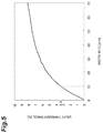
- FIG. 5 is a graph illustrating a relationship between a width of a light guide path and light transmissive efficiency.
- FIGS. 6A and 6B are cross-sectional views illustrating light guide portions according to other aspects.
- FIGS. 7A to 7C are cross-sectional views illustrating light guide portions according to still other aspects.
- a print head 1 is configured to include a light guide portion 10 and a light emitting element array 20 as illustrated in FIG. 1 .
- the light guide portion 10 has a square columnar outer shape, and extends in one direction.
- the extending direction of the light guide portion 10 will be referred to as a Z direction (first direction)
- a direction along one side of the light guide portion 10 in a square cross section orthogonal to the Z direction will be referred to as an X direction (second direction)
- a direction orthogonal to the X direction in the square cross section will be referred to as a Y direction.
- the light guide portion 10 is configured to include a light blocking part 11 and a plurality of light guide paths 12 .
- the light blocking part 11 is configured with a plurality of partition walls 11 a and a plurality of outer peripheral walls 11 b .
- the light blocking part 11 is made of a material having high light blocking property (for example, a black matrix material or a plating material).
- the light blocking part 11 has a lattice shape when viewed from the Z direction, and, more specifically, a square lattice shape. In other words, in an XY cross section (and an end surface) of the light guide portion 10 , the plurality of light guide paths 12 having a square shape are disposed in parallel.
- the light blocking part 11 includes four partition walls 11 a arranged in the X direction, four partition walls 11 a arranged in the Y direction, and four outer peripheral walls 11 b forming an outer peripheral surface of the light guide portion 10 , and has a lattice shape of five rows and five columns.
- the number of rows and columns of lattices of the light blocking part 11 may be changed as appropriate.
- the light guide paths 12 are air gaps defined by the light blocking part 11 .
- the light guide portion 10 includes twenty-five light guide paths 12 .
- An interval between the partition walls 11 a adjacent to each other (an interval between the partition wall 11 a and the outer peripheral wall 11 b ) of the light blocking part 11 is designed to be uniform, and thus the light guide paths 12 all have an identical opening dimension and an identical cross section dimension.
- the partition walls 11 a and the light guide paths 12 of the light blocking part 11 are alternately arranged in the X direction, and the partition walls 11 a and the light guide paths 12 of the light blocking part 11 are alternately arranged in the Y direction.
- a length L 1 of the light guide portion 10 in the Z direction is 100 to 300 ⁇ m (as an example, 150 ⁇ m).
- a length L 2 of the light guide portion 10 in the X direction and a length L 3 thereof in the Y direction are changed depending on the number of rows and columns of the lattices of the light blocking part 11 , and may be designed to be the same as or larger than a dimension of the light emitting element array 20 .
- a width W 11 of each of the partition walls 11 a arranged in the X direction is designed to be equal to or less than 15 ⁇ m, and is 10 ⁇ m as an example.
- Each of the partition walls 11 a arranged in the Y direction is designed to have the same width as the width W 11 of each of the partition walls 11 a arranged in the X direction.
- a width W 12 of each light guide path 12 in the X direction is designed to be 10 ⁇ m or more to 30 ⁇ m or less, and is 15 ⁇ m as an example.
- a width of each light guide path 12 in the Y direction is designed to be the same as the width W 12 .
- the length L 1 of the light guide portion 10 in the Z direction is designed to ten times the width W 12 of the light guide path 12 .
- Each light guide path 12 of the light blocking part 11 may be filled with a light transmissive member.
- Each light guide path 12 may be completely embedded with a light transmissive member.
- the light blocking part 11 of the light guide portion 10 may be formed through injection molding.
- a resin having light blocking property may be used as a constituent material of the light blocking part 11 .
- the light blocking part 11 may be formed through injection molding, and then each light guide path 12 may be filled with a light transmissive resin which is an example of the light transmissive member by using a photolithography technique or a nanoimprint technique.
- the light blocking part 11 of the light guide portion 10 may be formed by using a MEMS technique. In this case, silicon may be used as a constituent material of the light blocking part 11 .
- the light blocking part 11 may be formed by using the MEMS technique, and then each light guide path 12 may be filled with a light transmissive resin which is an example of the light transmissive member by using a photolithography technique or a nanoimprint technique.
- the light blocking part 11 may be formed after the light transmissive member is formed.
- a light transmissive resin which is an example of the light transmissive member is molded to a shape of the light guide path 12 by using a photolithography technique or a nanoimprint technique. After the light transmissive member is molded, a material having high light blocking material is caused to flow into voids of the light transmissive member, and thus the light blocking part 11 is formed.
- a black resin may be used as a constituent material of the light blocking part 11 .
- a base 22 is disposed on one end surface 10 a (a lower end surface in FIG. 1 ) side of the light guide portion 10 .
- the base 22 has a tabular shape, and is made of a light transmissive material.
- the base 22 is a glass substrate.
- a thickness (that is, a Z direction length) of the base 22 is 0.1 mm as an example.
- One surface 22 a of the base 22 faces the end surface 10 a of the light guide portion 10 , and is in contact with the end surface 10 a.
- the light emitting element array 20 is provided on the other surface 22 b of the base 22 .
- the light emitting element array 20 includes a plurality of organic EL elements 21 arranged at an equal interval.
- FIG. 1 illustrates the organic EL elements 21 arranged in the X direction, but the organic EL elements 21 of the light emitting element array 20 may be arranged in a lattice shape or a zigzag shape in an X-Y plane.
- a separation width W 21 of the organic EL elements 21 adjacent to each other in the X direction is 80 ⁇ m
- a width W 22 of the organic EL element 21 in the X direction is 80 ⁇ m.
- a width W 23 of the light emitting element array 20 may be designed to be smaller than the width (corresponding to L 2 in FIG. 2 ) of the light guide portion 10 .
- Each organic EL element 21 may have a square shape, a rectangular shape, or a polygonal shape (for example, an octagonal shape) when viewed from the Z direction.
- the organic EL element 21 is an organic EL element emitting monochromatic white light as an example.
- the organic EL element 21 has a structure in which an organic EL layer is interposed between a pair of electrodes in a thickness direction thereof (the thickness direction of the base 22 , that is, the Z direction).
- an electrode on the light guide portion 10 side is a transparent electrode made of, for example, indium tin oxide (ITO) or indium zinc oxide (IZO).
- ITO indium tin oxide
- IZO indium zinc oxide
- the organic EL layer is a layer containing at least an organic compound (light emitting material) which emits light due to injection of electrons or holes.
- the organic compound may be a low-molecular compound, and may be a high-molecular compound.
- the organic EL layer may include an electron injection layer, an electron transport layer, a hole injection layer, and a hole transport layer in addition to the light emitting layer containing the light emitting material.
- a light emitting material of the organic EL layer may be a fluorescent material, and may be a phosphorescent material.
- FIG. 1 a wiring or a drive circuit supplying drive power to each organic EL element 21 is not illustrated.
- the other end surface 10 b (an upper end surface in FIG. 1 ) of the light guide portion 10 is covered with a film 24 .
- the film 24 is provided to prevent dust from entering the inside of the light guide portion 10 .
- the film 24 may be omitted as appropriate.
- the print head 1 is provided with a holding member 26 surrounding the periphery of the light guide portion 10 on one surface 22 a of the base 22 .
- the holding member 26 holds the light guide portion 10 on the periphery of the light guide portion 10 .
- the holding member 26 is provided to be coplanar with the end surface 10 b of the light guide portion 10 .
- the holding member 26 may be made of a light blocking material, and may be made of a light transmissive material (for example, a light transmissive resin material such as an epoxy resin or an acrylic resin). In a case where the holding member 26 has light transmissive property, the holding member 26 may be made of the same material as that of a light transmissive member filling the light guide path 12 . There may be an aspect in which the print head 1 does not include the holding member 26 .
- each organic EL element 21 of the light emitting element array 20 which is a light source
- light is generated from each organic EL element 21 .
- the light generated from the organic EL element 21 is incident to each light guide path 12 from one end surface 10 a side of the light guide portion 10 via the base 22 .
- only light parallel to the extending direction (that is, the Z direction and the extending direction of the light guide portion 10 ) of the light guide path 12 or light substantially parallel thereto selectively passes through the light guide path 12 , and is emitted from the other end surface 10 b of the light guide portion 10 .
- the light incident to the light guide path 12 from the light emitting element array 20 passes through the light guide path 12 so as to be converted into light substantially parallel to the extending direction of the light guide path 12 , and thus directivity can be increased.
- high-directivity light is emitted from the end surface 10 b of the light guide portion 10 .
- An exposure target (not illustrated) of the print head 1 is disposed at a position facing the end surface 10 b of the light guide portion 10 .
- the exposure target is irradiated with high-directivity light from the print head 1 .
- the exposure target is disposed near the end surface 10 b of the light guide portion 10 from the viewpoint of realizing a high resolution, and is disposed near the end surface 10 b of the light guide portion 10 by about 100 ⁇ m as an example.
- the exposure target may be disposed to be brought into contact with the film 24 .
- the plurality of light guide paths 12 of the light guide portion 10 are designed with an identical width of 15 ⁇ m, and thus high exposure characteristics are realized. Specifically, since the plurality of light guide paths 12 of the light guide portion 10 are designed with an identical width of 30 ⁇ m or less, exposure unevenness which is one of exposure characteristics can be reduced. Since the plurality of light guide paths 12 of the light guide portion 10 are designed with an identical width of 10 ⁇ m or more, a light amount which is one of exposure characteristics can be sufficiently obtained.
- the present inventors have checked a relationship between the width W 12 of the light guide path 12 and a tonal ratio through simulation.
- light-ray tracking calculation was performed according to a Monte Carlo method by using optical system analysis software.
- a separation distance between an exposure target and the light guide path 12 was 100 ⁇ m. Simulation results are as illustrated in FIGS. 3A and 3B . In graphs of FIGS.
- a transverse axis expresses a position [ ⁇ m] in the X direction (main scanning direction), and a longitudinal axis expresses a tonal ratio.
- a tonal ratio of when the width W 12 of the light guide path 12 is 20 ⁇ m is indicated by a solid line
- a tonal ratio of when the width W 12 of the light guide path 12 is 30 ⁇ m is indicated by a dashed line.
- a tonal ratio of when the width W 12 of the light guide path 12 is 40 ⁇ m is indicated by a dot chain line
- a tonal ratio of when the width W 12 of the light guide path 12 is 50 ⁇ m is indicated by a two-dot chain line.
- the graph of FIG. 4 illustrates actually measured data indicating a relationship between the width W 12 of the light guide path 12 and a tonal ratio.
- a transverse axis expresses a position [mm] in the X direction
- a longitudinal axis expresses a tonal ratio.
- a tonal ratio of when the width W 12 of the light guide path 12 is 20 ⁇ m is indicated by a solid line
- a tonal ratio of when the width W 12 of the light guide path 12 is 30 ⁇ m is indicated by a dashed line
- a tonal ratio of when the width W 12 of the light guide path 12 is 50 ⁇ m is indicated by a dot chain line.
- the width W 12 of the light guide path 12 is designed to be equal to or less than 30 ⁇ m, and thus a cycle of exposure unevenness is reduced to about 1 ⁇ 3 compared with a case of the width W 12 of the light guide path 12 exceeds 30 ⁇ m.
- the width W 12 of the light guide path 12 is equal to or less than 30 ⁇ m, it is possible to realize high exposure characteristics.
- the exposure unevenness is caused by a shadow of the partition wall 11 a , does not occur in a case where the width W 22 of the organic EL element 21 is the same as the width W 12 of the light guide path 12 , the separation width W 21 of the organic EL elements 21 is the same as the width W 11 of the partition wall 11 a , and the organic EL element 21 is completely positioned with the light guide path 12 , but may occur in other cases.
- the exposure unevenness occurs in a case where the organic EL element 21 has the width W 22 larger than the width W 12 of the light guide path 12 .
- the organic EL element 21 has the width W 22 which is the same as the width W 12 of the light guide path 12 , it is considerably difficult to accurately position the organic EL element 21 with the light guide path 12 via the base 22 , and thus the exposure unevenness may occur.
- a resolution is increased, but the exposure unevenness easily occurs.
- the print head 1 can effectively reduce the exposure unevenness under the condition in which the exposure unevenness occurs.
- the present inventors have checked a relationship between the width W 12 of the light guide path 12 and a light transmittance through simulation in relation to a light amount which is one of the exposure characteristics.
- a measurement result is as illustrated in FIG. 5 .
- a transverse axis expresses the width W 12 [ ⁇ m] of the light guide path 12
- a longitudinal axis expresses a light transmittance [%].
- the width W 12 of the light guide path 12 at which a light transmittance is 3.3% is 10 ⁇ m
- the width W 12 of the light guide path 12 is designed to be equal to or more than 10 ⁇ m, and thus a sufficient light amount in practical use can be obtained.
- the width W 12 of the light guide path 12 is equal to or more than 10 ⁇ m, it is possible to realize higher exposure characteristics.
- the exposure unevenness may be reduced by separating an exposure target from the light guide portion 10 , or disposing an optical component such as a diffusion plate or a lens between an exposure target and the light guide portion 10 .
- problems such as a reduction in a resolution, an increase in a size of a device, an increase in the number of components, and complication of manufacturing steps occur.
- the print head 1 can reduce exposure unevenness while preventing the problems such as a reduction in a resolution, an increase in a size of a device, an increase in the number of components, and complication of manufacturing steps.
- the print head according to the present disclosure is not limited to the embodiment, and may be variously modified.
- light generated from an organic EL element may be monochromatic light such as red light or blue light instead of white light.
- a light emitting element configuring the light emitting element array is not limited to an organic EL element, and may be a liquid crystal element or a fluorescent display tube.
- a color filter may be provided between a light emitting element and a base, and colored light may be emitted from the end surface 10 b of the light guide portion 10 while using a light emitting element generating monochromatic white light.
- light may be colored to each color of RGB with color filters, and thus full-color light may be emitted from the end surface 10 b of the light guide portion 10 .
- the base 22 not only a glass substrate but also a silicon substrate or a plastic substrate may be used.
- the base 22 may be flexible, and, in this case, for example, a resin film such as a polyethylene terephthalate (PET) film or a polyimide (PI) film may be used.
- PET polyethylene terephthalate
- PI polyimide
- An opening shape and a cross-sectional shape of the light guide path of the light guide portion are not limited to a square shape, and may be a rectangular shape, a linear shape, and a polygonal shape, a circular shape, or an elliptical shape other than a quadrangular shape.
- the light guide path of the light guide portion may be disposed in a zigzag shape when viewed from the extending direction of the light guide portion.
- the number of light guide paths of the light guide portion or the number of light emitting elements may be changed as appropriate.
- An antireflection film which is formed through plating or heat treatment may be provided on an inner surface wall of the light guide path of the light guide portion in order to suppress reflection at the inner wall surface.
- the light guide portion may have aspects as illustrated in FIGS. 6A and 6B and FIGS. 7A to 7C .
- FIGS. 6A and 6B and FIGS. 7A to 7C all illustrate cross-sectional shapes of the light guide portion in an XY cross section orthogonal to the extending direction (Z direction) of the light guide paths.
- each of the light guide paths 12 of the light guide portion 10 illustrated in FIGS. 6A and 6B has a perfect circular cross-sectional shape (30 ⁇ m in diameter as an example), and each of the light guide paths 12 of the light guide portion 10 illustrated in FIG. 6B has a hexagonal cross-sectional shape (30 ⁇ m in width as an example).
- the plurality of light guide paths 12 are disposed in a zigzag shape at a predetermined interval (at 10 ⁇ m interval as an example).
- Each of the light guide paths 12 of the light guide portion 10 illustrated in FIG. 7A has a perfect circular cross-sectional shape (30 ⁇ m in diameter as an example)
- each of the light guide paths 12 of the light guide portion 10 illustrated in FIG. 7B has a hexagonal cross-sectional shape (30 ⁇ m in width as an example)
- each of the light guide paths 12 of the light guide portion 10 illustrated in FIG. 7C has a square cross-sectional shape (30 ⁇ m square as an example).
Landscapes
- Physics & Mathematics (AREA)
- General Physics & Mathematics (AREA)
- Optics & Photonics (AREA)
- Health & Medical Sciences (AREA)
- General Health & Medical Sciences (AREA)
- Toxicology (AREA)
- Printers Or Recording Devices Using Electromagnetic And Radiation Means (AREA)
- Electroluminescent Light Sources (AREA)
- Particle Formation And Scattering Control In Inkjet Printers (AREA)
- Impact Printers (AREA)
Applications Claiming Priority (2)
| Application Number | Priority Date | Filing Date | Title |
|---|---|---|---|
| JP2018-151210 | 2018-08-10 | ||
| JP2018151210 | 2018-08-10 |
Publications (2)
| Publication Number | Publication Date |
|---|---|
| US20200049879A1 US20200049879A1 (en) | 2020-02-13 |
| US10823902B2 true US10823902B2 (en) | 2020-11-03 |
Family
ID=69406990
Family Applications (1)
| Application Number | Title | Priority Date | Filing Date |
|---|---|---|---|
| US16/537,289 Active US10823902B2 (en) | 2018-08-10 | 2019-08-09 | Print head |
Country Status (4)
| Country | Link |
|---|---|
| US (1) | US10823902B2 (ja) |
| JP (1) | JP6752948B2 (ja) |
| CN (1) | CN110816075B (ja) |
| TW (1) | TWI777080B (ja) |
Cited By (1)
| Publication number | Priority date | Publication date | Assignee | Title |
|---|---|---|---|---|
| US20220077934A1 (en) * | 2020-09-10 | 2022-03-10 | Saco Technologies Inc. | Light shaping element and light shaping assembly |
Citations (18)
| Publication number | Priority date | Publication date | Assignee | Title |
|---|---|---|---|---|
| JPH10181089A (ja) | 1996-12-26 | 1998-07-07 | Ricoh Co Ltd | 光学装置 |
| CN1232994A (zh) | 1998-02-02 | 1999-10-27 | 双叶电子工业株式会社 | 光学印制机和光学印制头 |
| JP2000156285A (ja) | 1998-11-19 | 2000-06-06 | Canon Inc | 露光装置及び画像形成装置 |
| US20030202751A1 (en) * | 2000-12-29 | 2003-10-30 | Venkatesan Murali | Lithographically defined optic array |
| US20040179796A1 (en) * | 2001-03-09 | 2004-09-16 | Christian Jakobsen | Fabrication of microstructured fibres |
| US20050036029A1 (en) | 2000-12-12 | 2005-02-17 | Nissim Pilossof | Imaging head with laser diode array and a beam-shaping micro light-pipe array |
| JP2005271574A (ja) | 2003-11-05 | 2005-10-06 | Ricoh Co Ltd | 光書き込みユニット、画像形成装置、プロセスカートリッジ、光量調整方法 |
| US20050232560A1 (en) * | 2001-12-11 | 2005-10-20 | Blazephotonics Limited | Method and apparatus relating to optical fibre waveguides |
| TW200821780A (en) | 2006-09-29 | 2008-05-16 | Seiko Epson Corp | Electro-optical device and image forming apparatus |
| CN101308250A (zh) | 2007-05-14 | 2008-11-19 | 精工爱普生株式会社 | 遮光部件、行头及使用该行头的图像形成装置 |
| CN101408748A (zh) | 2007-07-20 | 2009-04-15 | 精工爱普生株式会社 | 行头及使用该行头的图像形成装置 |
| JP2009137107A (ja) | 2007-12-05 | 2009-06-25 | Seiko Epson Corp | ラインヘッドおよび該ラインヘッドを用いた画像形成装置 |
| JP2011131457A (ja) | 2009-12-24 | 2011-07-07 | Seiko Epson Corp | 光源装置および画像形成装置 |
| US20120223214A1 (en) * | 2011-03-03 | 2012-09-06 | California Institute Of Technology | Light Guided Pixel |
| US20140192515A1 (en) * | 2013-01-07 | 2014-07-10 | Samsung Display Co., Ltd. | Display device |
| WO2016080257A1 (ja) | 2014-11-21 | 2016-05-26 | コニカミノルタ株式会社 | 光源ユニット |
| CN206515603U (zh) | 2016-02-24 | 2017-09-22 | 双叶电子工业株式会社 | 光写入装置 |
| WO2018124012A1 (ja) | 2016-12-27 | 2018-07-05 | 大日本印刷株式会社 | スペーサー、面光源装置および画像表示装置 |
-
2019
- 2019-08-08 TW TW108128235A patent/TWI777080B/zh active
- 2019-08-08 CN CN201910729596.1A patent/CN110816075B/zh active Active
- 2019-08-09 US US16/537,289 patent/US10823902B2/en active Active
- 2019-08-09 JP JP2019147524A patent/JP6752948B2/ja not_active Expired - Fee Related
Patent Citations (19)
| Publication number | Priority date | Publication date | Assignee | Title |
|---|---|---|---|---|
| JPH10181089A (ja) | 1996-12-26 | 1998-07-07 | Ricoh Co Ltd | 光学装置 |
| CN1232994A (zh) | 1998-02-02 | 1999-10-27 | 双叶电子工业株式会社 | 光学印制机和光学印制头 |
| JP2000156285A (ja) | 1998-11-19 | 2000-06-06 | Canon Inc | 露光装置及び画像形成装置 |
| US20050036029A1 (en) | 2000-12-12 | 2005-02-17 | Nissim Pilossof | Imaging head with laser diode array and a beam-shaping micro light-pipe array |
| US20030202751A1 (en) * | 2000-12-29 | 2003-10-30 | Venkatesan Murali | Lithographically defined optic array |
| US20040179796A1 (en) * | 2001-03-09 | 2004-09-16 | Christian Jakobsen | Fabrication of microstructured fibres |
| US20050232560A1 (en) * | 2001-12-11 | 2005-10-20 | Blazephotonics Limited | Method and apparatus relating to optical fibre waveguides |
| JP2005271574A (ja) | 2003-11-05 | 2005-10-06 | Ricoh Co Ltd | 光書き込みユニット、画像形成装置、プロセスカートリッジ、光量調整方法 |
| TW200821780A (en) | 2006-09-29 | 2008-05-16 | Seiko Epson Corp | Electro-optical device and image forming apparatus |
| CN101308250A (zh) | 2007-05-14 | 2008-11-19 | 精工爱普生株式会社 | 遮光部件、行头及使用该行头的图像形成装置 |
| CN101408748A (zh) | 2007-07-20 | 2009-04-15 | 精工爱普生株式会社 | 行头及使用该行头的图像形成装置 |
| JP2009137107A (ja) | 2007-12-05 | 2009-06-25 | Seiko Epson Corp | ラインヘッドおよび該ラインヘッドを用いた画像形成装置 |
| JP2011131457A (ja) | 2009-12-24 | 2011-07-07 | Seiko Epson Corp | 光源装置および画像形成装置 |
| US20120223214A1 (en) * | 2011-03-03 | 2012-09-06 | California Institute Of Technology | Light Guided Pixel |
| US20140192515A1 (en) * | 2013-01-07 | 2014-07-10 | Samsung Display Co., Ltd. | Display device |
| WO2016080257A1 (ja) | 2014-11-21 | 2016-05-26 | コニカミノルタ株式会社 | 光源ユニット |
| CN107000447A (zh) | 2014-11-21 | 2017-08-01 | 柯尼卡美能达株式会社 | 光源单元 |
| CN206515603U (zh) | 2016-02-24 | 2017-09-22 | 双叶电子工业株式会社 | 光写入装置 |
| WO2018124012A1 (ja) | 2016-12-27 | 2018-07-05 | 大日本印刷株式会社 | スペーサー、面光源装置および画像表示装置 |
Cited By (2)
| Publication number | Priority date | Publication date | Assignee | Title |
|---|---|---|---|---|
| US20220077934A1 (en) * | 2020-09-10 | 2022-03-10 | Saco Technologies Inc. | Light shaping element and light shaping assembly |
| US11953193B2 (en) * | 2020-09-10 | 2024-04-09 | Saco Technologies Inc. | Light shaping element and light shaping assembly |
Also Published As
| Publication number | Publication date |
|---|---|
| US20200049879A1 (en) | 2020-02-13 |
| JP6752948B2 (ja) | 2020-09-09 |
| JP2020026139A (ja) | 2020-02-20 |
| TW202009144A (zh) | 2020-03-01 |
| CN110816075A (zh) | 2020-02-21 |
| CN110816075B (zh) | 2021-03-09 |
| TWI777080B (zh) | 2022-09-11 |
Similar Documents
| Publication | Publication Date | Title |
|---|---|---|
| US11061276B2 (en) | Laser array display | |
| US9853241B2 (en) | Organic light-emitting display apparatus and fabrication method thereof | |
| US10431719B2 (en) | Display with color conversion | |
| KR100817577B1 (ko) | 탄소 나노튜브 전계방출 표시장치 | |
| KR102226567B1 (ko) | 표시 장치 | |
| US20070183136A1 (en) | Backlight assembly and display device having the same | |
| US11143915B2 (en) | Lighting device including light guide plate and display device including the lighting device | |
| US11239295B2 (en) | Organic light-emitting display devices, methods for manufacturing the same, and masks for making supporting members | |
| US20180277610A1 (en) | Electrooptical device, manufacturing method of electrooptical device, and electronic equipment | |
| TW202029166A (zh) | 全彩led顯示面板 | |
| JP2014049367A (ja) | 表示装置 | |
| TW200421930A (en) | Area light emitting device, method for manufacturing the same, and liquid crystal display unit | |
| CN108630672B (zh) | 影像显示模块及其制作方法、及显示设备 | |
| KR102590433B1 (ko) | 디스플레이 모듈, 이를 포함하는 디스플레이 장치 및 디스플레이 모듈 제조 방법 | |
| CN111081685B (zh) | 显示装置 | |
| US10823902B2 (en) | Print head | |
| US20150146132A1 (en) | Surface light source device, display device, and lighting device | |
| JP2004111119A (ja) | 表示装置およびその製造方法 | |
| JP6649332B2 (ja) | プリントヘッド | |
| CN111247577A (zh) | 显示装置 | |
| KR102657295B1 (ko) | 유기발광장치 | |
| CN114419994A (zh) | 背光模组 | |
| WO2020100862A1 (ja) | 表示装置およびその製造方法、電子機器および照明装置 | |
| CN113711088A (zh) | 显示装置和电子设备 | |
| JP2020097198A (ja) | プリントヘッド |
Legal Events
| Date | Code | Title | Description |
|---|---|---|---|
| FEPP | Fee payment procedure |
Free format text: ENTITY STATUS SET TO UNDISCOUNTED (ORIGINAL EVENT CODE: BIG.); ENTITY STATUS OF PATENT OWNER: LARGE ENTITY |
|
| STPP | Information on status: patent application and granting procedure in general |
Free format text: DOCKETED NEW CASE - READY FOR EXAMINATION |
|
| AS | Assignment |
Owner name: FUTABA CORPORATION, JAPAN Free format text: ASSIGNMENT OF ASSIGNORS INTEREST;ASSIGNOR:SATO, TOMOYA;REEL/FRAME:050781/0548 Effective date: 20190902 |
|
| STPP | Information on status: patent application and granting procedure in general |
Free format text: NOTICE OF ALLOWANCE MAILED -- APPLICATION RECEIVED IN OFFICE OF PUBLICATIONS |
|
| STPP | Information on status: patent application and granting procedure in general |
Free format text: NOTICE OF ALLOWANCE MAILED -- APPLICATION RECEIVED IN OFFICE OF PUBLICATIONS |
|
| STPP | Information on status: patent application and granting procedure in general |
Free format text: PUBLICATIONS -- ISSUE FEE PAYMENT VERIFIED |
|
| STCF | Information on status: patent grant |
Free format text: PATENTED CASE |