US10809561B2 - Display panel - Google Patents
Display panel Download PDFInfo
- Publication number
- US10809561B2 US10809561B2 US16/033,248 US201816033248A US10809561B2 US 10809561 B2 US10809561 B2 US 10809561B2 US 201816033248 A US201816033248 A US 201816033248A US 10809561 B2 US10809561 B2 US 10809561B2
- Authority
- US
- United States
- Prior art keywords
- substrate
- extending direction
- electrodes
- display panel
- disposed
- Prior art date
- Legal status (The legal status is an assumption and is not a legal conclusion. Google has not performed a legal analysis and makes no representation as to the accuracy of the status listed.)
- Active, expires
Links
- 239000000758 substrate Substances 0.000 claims abstract description 158
- 239000004973 liquid crystal related substance Substances 0.000 claims abstract description 65
- 230000003287 optical effect Effects 0.000 claims description 13
- 239000010408 film Substances 0.000 description 61
- 238000000034 method Methods 0.000 description 26
- 238000004519 manufacturing process Methods 0.000 description 13
- 230000000694 effects Effects 0.000 description 6
- 238000000926 separation method Methods 0.000 description 6
- 239000004065 semiconductor Substances 0.000 description 3
- 230000001154 acute effect Effects 0.000 description 2
- 230000008901 benefit Effects 0.000 description 2
- 238000005530 etching Methods 0.000 description 2
- 239000000463 material Substances 0.000 description 2
- 238000012986 modification Methods 0.000 description 2
- 230000004048 modification Effects 0.000 description 2
- 238000000206 photolithography Methods 0.000 description 2
- OFIYHXOOOISSDN-UHFFFAOYSA-N tellanylidenegallium Chemical compound [Te]=[Ga] OFIYHXOOOISSDN-UHFFFAOYSA-N 0.000 description 2
- 230000005684 electric field Effects 0.000 description 1
- 239000011521 glass Substances 0.000 description 1
- 229920000620 organic polymer Polymers 0.000 description 1
- 230000010287 polarization Effects 0.000 description 1
- 239000010453 quartz Substances 0.000 description 1
- VYPSYNLAJGMNEJ-UHFFFAOYSA-N silicon dioxide Inorganic materials O=[Si]=O VYPSYNLAJGMNEJ-UHFFFAOYSA-N 0.000 description 1
Images


Classifications
-
- G—PHYSICS
- G06—COMPUTING; CALCULATING OR COUNTING
- G06F—ELECTRIC DIGITAL DATA PROCESSING
- G06F3/00—Input arrangements for transferring data to be processed into a form capable of being handled by the computer; Output arrangements for transferring data from processing unit to output unit, e.g. interface arrangements
- G06F3/01—Input arrangements or combined input and output arrangements for interaction between user and computer
- G06F3/03—Arrangements for converting the position or the displacement of a member into a coded form
- G06F3/041—Digitisers, e.g. for touch screens or touch pads, characterised by the transducing means
- G06F3/0412—Digitisers structurally integrated in a display
-
- G—PHYSICS
- G02—OPTICS
- G02F—OPTICAL DEVICES OR ARRANGEMENTS FOR THE CONTROL OF LIGHT BY MODIFICATION OF THE OPTICAL PROPERTIES OF THE MEDIA OF THE ELEMENTS INVOLVED THEREIN; NON-LINEAR OPTICS; FREQUENCY-CHANGING OF LIGHT; OPTICAL LOGIC ELEMENTS; OPTICAL ANALOGUE/DIGITAL CONVERTERS
- G02F1/00—Devices or arrangements for the control of the intensity, colour, phase, polarisation or direction of light arriving from an independent light source, e.g. switching, gating or modulating; Non-linear optics
- G02F1/01—Devices or arrangements for the control of the intensity, colour, phase, polarisation or direction of light arriving from an independent light source, e.g. switching, gating or modulating; Non-linear optics for the control of the intensity, phase, polarisation or colour
- G02F1/13—Devices or arrangements for the control of the intensity, colour, phase, polarisation or direction of light arriving from an independent light source, e.g. switching, gating or modulating; Non-linear optics for the control of the intensity, phase, polarisation or colour based on liquid crystals, e.g. single liquid crystal display cells
- G02F1/133—Constructional arrangements; Operation of liquid crystal cells; Circuit arrangements
- G02F1/1333—Constructional arrangements; Manufacturing methods
- G02F1/1335—Structural association of cells with optical devices, e.g. polarisers or reflectors
- G02F1/133528—Polarisers
-
- G—PHYSICS
- G02—OPTICS
- G02F—OPTICAL DEVICES OR ARRANGEMENTS FOR THE CONTROL OF LIGHT BY MODIFICATION OF THE OPTICAL PROPERTIES OF THE MEDIA OF THE ELEMENTS INVOLVED THEREIN; NON-LINEAR OPTICS; FREQUENCY-CHANGING OF LIGHT; OPTICAL LOGIC ELEMENTS; OPTICAL ANALOGUE/DIGITAL CONVERTERS
- G02F1/00—Devices or arrangements for the control of the intensity, colour, phase, polarisation or direction of light arriving from an independent light source, e.g. switching, gating or modulating; Non-linear optics
- G02F1/01—Devices or arrangements for the control of the intensity, colour, phase, polarisation or direction of light arriving from an independent light source, e.g. switching, gating or modulating; Non-linear optics for the control of the intensity, phase, polarisation or colour
- G02F1/13—Devices or arrangements for the control of the intensity, colour, phase, polarisation or direction of light arriving from an independent light source, e.g. switching, gating or modulating; Non-linear optics for the control of the intensity, phase, polarisation or colour based on liquid crystals, e.g. single liquid crystal display cells
- G02F1/133—Constructional arrangements; Operation of liquid crystal cells; Circuit arrangements
- G02F1/136—Liquid crystal cells structurally associated with a semi-conducting layer or substrate, e.g. cells forming part of an integrated circuit
- G02F1/1362—Active matrix addressed cells
- G02F1/136286—Wiring, e.g. gate line, drain line
-
- G—PHYSICS
- G02—OPTICS
- G02F—OPTICAL DEVICES OR ARRANGEMENTS FOR THE CONTROL OF LIGHT BY MODIFICATION OF THE OPTICAL PROPERTIES OF THE MEDIA OF THE ELEMENTS INVOLVED THEREIN; NON-LINEAR OPTICS; FREQUENCY-CHANGING OF LIGHT; OPTICAL LOGIC ELEMENTS; OPTICAL ANALOGUE/DIGITAL CONVERTERS
- G02F1/00—Devices or arrangements for the control of the intensity, colour, phase, polarisation or direction of light arriving from an independent light source, e.g. switching, gating or modulating; Non-linear optics
- G02F1/01—Devices or arrangements for the control of the intensity, colour, phase, polarisation or direction of light arriving from an independent light source, e.g. switching, gating or modulating; Non-linear optics for the control of the intensity, phase, polarisation or colour
- G02F1/13—Devices or arrangements for the control of the intensity, colour, phase, polarisation or direction of light arriving from an independent light source, e.g. switching, gating or modulating; Non-linear optics for the control of the intensity, phase, polarisation or colour based on liquid crystals, e.g. single liquid crystal display cells
- G02F1/1323—Arrangements for providing a switchable viewing angle
-
- G—PHYSICS
- G02—OPTICS
- G02F—OPTICAL DEVICES OR ARRANGEMENTS FOR THE CONTROL OF LIGHT BY MODIFICATION OF THE OPTICAL PROPERTIES OF THE MEDIA OF THE ELEMENTS INVOLVED THEREIN; NON-LINEAR OPTICS; FREQUENCY-CHANGING OF LIGHT; OPTICAL LOGIC ELEMENTS; OPTICAL ANALOGUE/DIGITAL CONVERTERS
- G02F1/00—Devices or arrangements for the control of the intensity, colour, phase, polarisation or direction of light arriving from an independent light source, e.g. switching, gating or modulating; Non-linear optics
- G02F1/01—Devices or arrangements for the control of the intensity, colour, phase, polarisation or direction of light arriving from an independent light source, e.g. switching, gating or modulating; Non-linear optics for the control of the intensity, phase, polarisation or colour
- G02F1/13—Devices or arrangements for the control of the intensity, colour, phase, polarisation or direction of light arriving from an independent light source, e.g. switching, gating or modulating; Non-linear optics for the control of the intensity, phase, polarisation or colour based on liquid crystals, e.g. single liquid crystal display cells
- G02F1/133—Constructional arrangements; Operation of liquid crystal cells; Circuit arrangements
- G02F1/1333—Constructional arrangements; Manufacturing methods
- G02F1/13338—Input devices, e.g. touch panels
-
- G—PHYSICS
- G02—OPTICS
- G02F—OPTICAL DEVICES OR ARRANGEMENTS FOR THE CONTROL OF LIGHT BY MODIFICATION OF THE OPTICAL PROPERTIES OF THE MEDIA OF THE ELEMENTS INVOLVED THEREIN; NON-LINEAR OPTICS; FREQUENCY-CHANGING OF LIGHT; OPTICAL LOGIC ELEMENTS; OPTICAL ANALOGUE/DIGITAL CONVERTERS
- G02F1/00—Devices or arrangements for the control of the intensity, colour, phase, polarisation or direction of light arriving from an independent light source, e.g. switching, gating or modulating; Non-linear optics
- G02F1/01—Devices or arrangements for the control of the intensity, colour, phase, polarisation or direction of light arriving from an independent light source, e.g. switching, gating or modulating; Non-linear optics for the control of the intensity, phase, polarisation or colour
- G02F1/13—Devices or arrangements for the control of the intensity, colour, phase, polarisation or direction of light arriving from an independent light source, e.g. switching, gating or modulating; Non-linear optics for the control of the intensity, phase, polarisation or colour based on liquid crystals, e.g. single liquid crystal display cells
- G02F1/133—Constructional arrangements; Operation of liquid crystal cells; Circuit arrangements
- G02F1/1333—Constructional arrangements; Manufacturing methods
- G02F1/1337—Surface-induced orientation of the liquid crystal molecules, e.g. by alignment layers
- G02F1/133707—Structures for producing distorted electric fields, e.g. bumps, protrusions, recesses, slits in pixel electrodes
-
- G—PHYSICS
- G02—OPTICS
- G02F—OPTICAL DEVICES OR ARRANGEMENTS FOR THE CONTROL OF LIGHT BY MODIFICATION OF THE OPTICAL PROPERTIES OF THE MEDIA OF THE ELEMENTS INVOLVED THEREIN; NON-LINEAR OPTICS; FREQUENCY-CHANGING OF LIGHT; OPTICAL LOGIC ELEMENTS; OPTICAL ANALOGUE/DIGITAL CONVERTERS
- G02F1/00—Devices or arrangements for the control of the intensity, colour, phase, polarisation or direction of light arriving from an independent light source, e.g. switching, gating or modulating; Non-linear optics
- G02F1/01—Devices or arrangements for the control of the intensity, colour, phase, polarisation or direction of light arriving from an independent light source, e.g. switching, gating or modulating; Non-linear optics for the control of the intensity, phase, polarisation or colour
- G02F1/13—Devices or arrangements for the control of the intensity, colour, phase, polarisation or direction of light arriving from an independent light source, e.g. switching, gating or modulating; Non-linear optics for the control of the intensity, phase, polarisation or colour based on liquid crystals, e.g. single liquid crystal display cells
- G02F1/133—Constructional arrangements; Operation of liquid crystal cells; Circuit arrangements
- G02F1/1333—Constructional arrangements; Manufacturing methods
- G02F1/1343—Electrodes
- G02F1/134309—Electrodes characterised by their geometrical arrangement
- G02F1/134336—Matrix
-
- G—PHYSICS
- G02—OPTICS
- G02F—OPTICAL DEVICES OR ARRANGEMENTS FOR THE CONTROL OF LIGHT BY MODIFICATION OF THE OPTICAL PROPERTIES OF THE MEDIA OF THE ELEMENTS INVOLVED THEREIN; NON-LINEAR OPTICS; FREQUENCY-CHANGING OF LIGHT; OPTICAL LOGIC ELEMENTS; OPTICAL ANALOGUE/DIGITAL CONVERTERS
- G02F1/00—Devices or arrangements for the control of the intensity, colour, phase, polarisation or direction of light arriving from an independent light source, e.g. switching, gating or modulating; Non-linear optics
- G02F1/01—Devices or arrangements for the control of the intensity, colour, phase, polarisation or direction of light arriving from an independent light source, e.g. switching, gating or modulating; Non-linear optics for the control of the intensity, phase, polarisation or colour
- G02F1/13—Devices or arrangements for the control of the intensity, colour, phase, polarisation or direction of light arriving from an independent light source, e.g. switching, gating or modulating; Non-linear optics for the control of the intensity, phase, polarisation or colour based on liquid crystals, e.g. single liquid crystal display cells
- G02F1/133—Constructional arrangements; Operation of liquid crystal cells; Circuit arrangements
- G02F1/1333—Constructional arrangements; Manufacturing methods
- G02F1/1343—Electrodes
- G02F1/134309—Electrodes characterised by their geometrical arrangement
- G02F1/134363—Electrodes characterised by their geometrical arrangement for applying an electric field parallel to the substrate, i.e. in-plane switching [IPS]
-
- G—PHYSICS
- G02—OPTICS
- G02F—OPTICAL DEVICES OR ARRANGEMENTS FOR THE CONTROL OF LIGHT BY MODIFICATION OF THE OPTICAL PROPERTIES OF THE MEDIA OF THE ELEMENTS INVOLVED THEREIN; NON-LINEAR OPTICS; FREQUENCY-CHANGING OF LIGHT; OPTICAL LOGIC ELEMENTS; OPTICAL ANALOGUE/DIGITAL CONVERTERS
- G02F1/00—Devices or arrangements for the control of the intensity, colour, phase, polarisation or direction of light arriving from an independent light source, e.g. switching, gating or modulating; Non-linear optics
- G02F1/01—Devices or arrangements for the control of the intensity, colour, phase, polarisation or direction of light arriving from an independent light source, e.g. switching, gating or modulating; Non-linear optics for the control of the intensity, phase, polarisation or colour
- G02F1/13—Devices or arrangements for the control of the intensity, colour, phase, polarisation or direction of light arriving from an independent light source, e.g. switching, gating or modulating; Non-linear optics for the control of the intensity, phase, polarisation or colour based on liquid crystals, e.g. single liquid crystal display cells
- G02F1/133—Constructional arrangements; Operation of liquid crystal cells; Circuit arrangements
- G02F1/136—Liquid crystal cells structurally associated with a semi-conducting layer or substrate, e.g. cells forming part of an integrated circuit
- G02F1/1362—Active matrix addressed cells
- G02F1/1368—Active matrix addressed cells in which the switching element is a three-electrode device
-
- G—PHYSICS
- G02—OPTICS
- G02F—OPTICAL DEVICES OR ARRANGEMENTS FOR THE CONTROL OF LIGHT BY MODIFICATION OF THE OPTICAL PROPERTIES OF THE MEDIA OF THE ELEMENTS INVOLVED THEREIN; NON-LINEAR OPTICS; FREQUENCY-CHANGING OF LIGHT; OPTICAL LOGIC ELEMENTS; OPTICAL ANALOGUE/DIGITAL CONVERTERS
- G02F1/00—Devices or arrangements for the control of the intensity, colour, phase, polarisation or direction of light arriving from an independent light source, e.g. switching, gating or modulating; Non-linear optics
- G02F1/01—Devices or arrangements for the control of the intensity, colour, phase, polarisation or direction of light arriving from an independent light source, e.g. switching, gating or modulating; Non-linear optics for the control of the intensity, phase, polarisation or colour
- G02F1/13—Devices or arrangements for the control of the intensity, colour, phase, polarisation or direction of light arriving from an independent light source, e.g. switching, gating or modulating; Non-linear optics for the control of the intensity, phase, polarisation or colour based on liquid crystals, e.g. single liquid crystal display cells
- G02F1/137—Devices or arrangements for the control of the intensity, colour, phase, polarisation or direction of light arriving from an independent light source, e.g. switching, gating or modulating; Non-linear optics for the control of the intensity, phase, polarisation or colour based on liquid crystals, e.g. single liquid crystal display cells characterised by the electro-optical or magneto-optical effect, e.g. field-induced phase transition, orientation effect, guest-host interaction or dynamic scattering
-
- G—PHYSICS
- G02—OPTICS
- G02F—OPTICAL DEVICES OR ARRANGEMENTS FOR THE CONTROL OF LIGHT BY MODIFICATION OF THE OPTICAL PROPERTIES OF THE MEDIA OF THE ELEMENTS INVOLVED THEREIN; NON-LINEAR OPTICS; FREQUENCY-CHANGING OF LIGHT; OPTICAL LOGIC ELEMENTS; OPTICAL ANALOGUE/DIGITAL CONVERTERS
- G02F1/00—Devices or arrangements for the control of the intensity, colour, phase, polarisation or direction of light arriving from an independent light source, e.g. switching, gating or modulating; Non-linear optics
- G02F1/01—Devices or arrangements for the control of the intensity, colour, phase, polarisation or direction of light arriving from an independent light source, e.g. switching, gating or modulating; Non-linear optics for the control of the intensity, phase, polarisation or colour
- G02F1/13—Devices or arrangements for the control of the intensity, colour, phase, polarisation or direction of light arriving from an independent light source, e.g. switching, gating or modulating; Non-linear optics for the control of the intensity, phase, polarisation or colour based on liquid crystals, e.g. single liquid crystal display cells
- G02F1/133—Constructional arrangements; Operation of liquid crystal cells; Circuit arrangements
- G02F1/1333—Constructional arrangements; Manufacturing methods
- G02F1/1335—Structural association of cells with optical devices, e.g. polarisers or reflectors
- G02F1/133528—Polarisers
- G02F1/133531—Polarisers characterised by the arrangement of polariser or analyser axes
-
- G—PHYSICS
- G02—OPTICS
- G02F—OPTICAL DEVICES OR ARRANGEMENTS FOR THE CONTROL OF LIGHT BY MODIFICATION OF THE OPTICAL PROPERTIES OF THE MEDIA OF THE ELEMENTS INVOLVED THEREIN; NON-LINEAR OPTICS; FREQUENCY-CHANGING OF LIGHT; OPTICAL LOGIC ELEMENTS; OPTICAL ANALOGUE/DIGITAL CONVERTERS
- G02F1/00—Devices or arrangements for the control of the intensity, colour, phase, polarisation or direction of light arriving from an independent light source, e.g. switching, gating or modulating; Non-linear optics
- G02F1/01—Devices or arrangements for the control of the intensity, colour, phase, polarisation or direction of light arriving from an independent light source, e.g. switching, gating or modulating; Non-linear optics for the control of the intensity, phase, polarisation or colour
- G02F1/13—Devices or arrangements for the control of the intensity, colour, phase, polarisation or direction of light arriving from an independent light source, e.g. switching, gating or modulating; Non-linear optics for the control of the intensity, phase, polarisation or colour based on liquid crystals, e.g. single liquid crystal display cells
- G02F1/133—Constructional arrangements; Operation of liquid crystal cells; Circuit arrangements
- G02F1/1333—Constructional arrangements; Manufacturing methods
- G02F1/1335—Structural association of cells with optical devices, e.g. polarisers or reflectors
- G02F1/133528—Polarisers
- G02F1/133548—Wire-grid polarisers
-
- G—PHYSICS
- G02—OPTICS
- G02F—OPTICAL DEVICES OR ARRANGEMENTS FOR THE CONTROL OF LIGHT BY MODIFICATION OF THE OPTICAL PROPERTIES OF THE MEDIA OF THE ELEMENTS INVOLVED THEREIN; NON-LINEAR OPTICS; FREQUENCY-CHANGING OF LIGHT; OPTICAL LOGIC ELEMENTS; OPTICAL ANALOGUE/DIGITAL CONVERTERS
- G02F1/00—Devices or arrangements for the control of the intensity, colour, phase, polarisation or direction of light arriving from an independent light source, e.g. switching, gating or modulating; Non-linear optics
- G02F1/01—Devices or arrangements for the control of the intensity, colour, phase, polarisation or direction of light arriving from an independent light source, e.g. switching, gating or modulating; Non-linear optics for the control of the intensity, phase, polarisation or colour
- G02F1/13—Devices or arrangements for the control of the intensity, colour, phase, polarisation or direction of light arriving from an independent light source, e.g. switching, gating or modulating; Non-linear optics for the control of the intensity, phase, polarisation or colour based on liquid crystals, e.g. single liquid crystal display cells
- G02F1/133—Constructional arrangements; Operation of liquid crystal cells; Circuit arrangements
- G02F1/1333—Constructional arrangements; Manufacturing methods
- G02F1/1335—Structural association of cells with optical devices, e.g. polarisers or reflectors
- G02F1/13356—Structural association of cells with optical devices, e.g. polarisers or reflectors characterised by the placement of the optical elements
- G02F1/133565—Structural association of cells with optical devices, e.g. polarisers or reflectors characterised by the placement of the optical elements inside the LC elements, i.e. between the cell substrates
-
- G—PHYSICS
- G02—OPTICS
- G02F—OPTICAL DEVICES OR ARRANGEMENTS FOR THE CONTROL OF LIGHT BY MODIFICATION OF THE OPTICAL PROPERTIES OF THE MEDIA OF THE ELEMENTS INVOLVED THEREIN; NON-LINEAR OPTICS; FREQUENCY-CHANGING OF LIGHT; OPTICAL LOGIC ELEMENTS; OPTICAL ANALOGUE/DIGITAL CONVERTERS
- G02F1/00—Devices or arrangements for the control of the intensity, colour, phase, polarisation or direction of light arriving from an independent light source, e.g. switching, gating or modulating; Non-linear optics
- G02F1/01—Devices or arrangements for the control of the intensity, colour, phase, polarisation or direction of light arriving from an independent light source, e.g. switching, gating or modulating; Non-linear optics for the control of the intensity, phase, polarisation or colour
- G02F1/13—Devices or arrangements for the control of the intensity, colour, phase, polarisation or direction of light arriving from an independent light source, e.g. switching, gating or modulating; Non-linear optics for the control of the intensity, phase, polarisation or colour based on liquid crystals, e.g. single liquid crystal display cells
- G02F1/133—Constructional arrangements; Operation of liquid crystal cells; Circuit arrangements
- G02F1/1333—Constructional arrangements; Manufacturing methods
- G02F1/1343—Electrodes
- G02F1/134309—Electrodes characterised by their geometrical arrangement
- G02F1/134318—Electrodes characterised by their geometrical arrangement having a patterned common electrode
-
- G—PHYSICS
- G02—OPTICS
- G02F—OPTICAL DEVICES OR ARRANGEMENTS FOR THE CONTROL OF LIGHT BY MODIFICATION OF THE OPTICAL PROPERTIES OF THE MEDIA OF THE ELEMENTS INVOLVED THEREIN; NON-LINEAR OPTICS; FREQUENCY-CHANGING OF LIGHT; OPTICAL LOGIC ELEMENTS; OPTICAL ANALOGUE/DIGITAL CONVERTERS
- G02F1/00—Devices or arrangements for the control of the intensity, colour, phase, polarisation or direction of light arriving from an independent light source, e.g. switching, gating or modulating; Non-linear optics
- G02F1/01—Devices or arrangements for the control of the intensity, colour, phase, polarisation or direction of light arriving from an independent light source, e.g. switching, gating or modulating; Non-linear optics for the control of the intensity, phase, polarisation or colour
- G02F1/13—Devices or arrangements for the control of the intensity, colour, phase, polarisation or direction of light arriving from an independent light source, e.g. switching, gating or modulating; Non-linear optics for the control of the intensity, phase, polarisation or colour based on liquid crystals, e.g. single liquid crystal display cells
- G02F1/133—Constructional arrangements; Operation of liquid crystal cells; Circuit arrangements
- G02F1/1333—Constructional arrangements; Manufacturing methods
- G02F1/1343—Electrodes
- G02F1/134309—Electrodes characterised by their geometrical arrangement
- G02F1/134372—Electrodes characterised by their geometrical arrangement for fringe field switching [FFS] where the common electrode is not patterned
-
- G—PHYSICS
- G02—OPTICS
- G02F—OPTICAL DEVICES OR ARRANGEMENTS FOR THE CONTROL OF LIGHT BY MODIFICATION OF THE OPTICAL PROPERTIES OF THE MEDIA OF THE ELEMENTS INVOLVED THEREIN; NON-LINEAR OPTICS; FREQUENCY-CHANGING OF LIGHT; OPTICAL LOGIC ELEMENTS; OPTICAL ANALOGUE/DIGITAL CONVERTERS
- G02F1/00—Devices or arrangements for the control of the intensity, colour, phase, polarisation or direction of light arriving from an independent light source, e.g. switching, gating or modulating; Non-linear optics
- G02F1/01—Devices or arrangements for the control of the intensity, colour, phase, polarisation or direction of light arriving from an independent light source, e.g. switching, gating or modulating; Non-linear optics for the control of the intensity, phase, polarisation or colour
- G02F1/13—Devices or arrangements for the control of the intensity, colour, phase, polarisation or direction of light arriving from an independent light source, e.g. switching, gating or modulating; Non-linear optics for the control of the intensity, phase, polarisation or colour based on liquid crystals, e.g. single liquid crystal display cells
- G02F1/137—Devices or arrangements for the control of the intensity, colour, phase, polarisation or direction of light arriving from an independent light source, e.g. switching, gating or modulating; Non-linear optics for the control of the intensity, phase, polarisation or colour based on liquid crystals, e.g. single liquid crystal display cells characterised by the electro-optical or magneto-optical effect, e.g. field-induced phase transition, orientation effect, guest-host interaction or dynamic scattering
- G02F1/13706—Devices or arrangements for the control of the intensity, colour, phase, polarisation or direction of light arriving from an independent light source, e.g. switching, gating or modulating; Non-linear optics for the control of the intensity, phase, polarisation or colour based on liquid crystals, e.g. single liquid crystal display cells characterised by the electro-optical or magneto-optical effect, e.g. field-induced phase transition, orientation effect, guest-host interaction or dynamic scattering the liquid crystal having positive dielectric anisotropy
-
- G—PHYSICS
- G02—OPTICS
- G02F—OPTICAL DEVICES OR ARRANGEMENTS FOR THE CONTROL OF LIGHT BY MODIFICATION OF THE OPTICAL PROPERTIES OF THE MEDIA OF THE ELEMENTS INVOLVED THEREIN; NON-LINEAR OPTICS; FREQUENCY-CHANGING OF LIGHT; OPTICAL LOGIC ELEMENTS; OPTICAL ANALOGUE/DIGITAL CONVERTERS
- G02F1/00—Devices or arrangements for the control of the intensity, colour, phase, polarisation or direction of light arriving from an independent light source, e.g. switching, gating or modulating; Non-linear optics
- G02F1/01—Devices or arrangements for the control of the intensity, colour, phase, polarisation or direction of light arriving from an independent light source, e.g. switching, gating or modulating; Non-linear optics for the control of the intensity, phase, polarisation or colour
- G02F1/13—Devices or arrangements for the control of the intensity, colour, phase, polarisation or direction of light arriving from an independent light source, e.g. switching, gating or modulating; Non-linear optics for the control of the intensity, phase, polarisation or colour based on liquid crystals, e.g. single liquid crystal display cells
- G02F1/137—Devices or arrangements for the control of the intensity, colour, phase, polarisation or direction of light arriving from an independent light source, e.g. switching, gating or modulating; Non-linear optics for the control of the intensity, phase, polarisation or colour based on liquid crystals, e.g. single liquid crystal display cells characterised by the electro-optical or magneto-optical effect, e.g. field-induced phase transition, orientation effect, guest-host interaction or dynamic scattering
- G02F1/13712—Devices or arrangements for the control of the intensity, colour, phase, polarisation or direction of light arriving from an independent light source, e.g. switching, gating or modulating; Non-linear optics for the control of the intensity, phase, polarisation or colour based on liquid crystals, e.g. single liquid crystal display cells characterised by the electro-optical or magneto-optical effect, e.g. field-induced phase transition, orientation effect, guest-host interaction or dynamic scattering the liquid crystal having negative dielectric anisotropy
-
- G02F2001/133531—
-
- G02F2001/133548—
-
- G02F2001/133565—
-
- G02F2001/134318—
-
- G02F2001/134372—
-
- G02F2001/13706—
-
- G02F2001/13712—
-
- G—PHYSICS
- G02—OPTICS
- G02F—OPTICAL DEVICES OR ARRANGEMENTS FOR THE CONTROL OF LIGHT BY MODIFICATION OF THE OPTICAL PROPERTIES OF THE MEDIA OF THE ELEMENTS INVOLVED THEREIN; NON-LINEAR OPTICS; FREQUENCY-CHANGING OF LIGHT; OPTICAL LOGIC ELEMENTS; OPTICAL ANALOGUE/DIGITAL CONVERTERS
- G02F2201/00—Constructional arrangements not provided for in groups G02F1/00 - G02F7/00
- G02F2201/12—Constructional arrangements not provided for in groups G02F1/00 - G02F7/00 electrode
- G02F2201/121—Constructional arrangements not provided for in groups G02F1/00 - G02F7/00 electrode common or background
-
- G—PHYSICS
- G02—OPTICS
- G02F—OPTICAL DEVICES OR ARRANGEMENTS FOR THE CONTROL OF LIGHT BY MODIFICATION OF THE OPTICAL PROPERTIES OF THE MEDIA OF THE ELEMENTS INVOLVED THEREIN; NON-LINEAR OPTICS; FREQUENCY-CHANGING OF LIGHT; OPTICAL LOGIC ELEMENTS; OPTICAL ANALOGUE/DIGITAL CONVERTERS
- G02F2201/00—Constructional arrangements not provided for in groups G02F1/00 - G02F7/00
- G02F2201/12—Constructional arrangements not provided for in groups G02F1/00 - G02F7/00 electrode
- G02F2201/123—Constructional arrangements not provided for in groups G02F1/00 - G02F7/00 electrode pixel
-
- G—PHYSICS
- G02—OPTICS
- G02F—OPTICAL DEVICES OR ARRANGEMENTS FOR THE CONTROL OF LIGHT BY MODIFICATION OF THE OPTICAL PROPERTIES OF THE MEDIA OF THE ELEMENTS INVOLVED THEREIN; NON-LINEAR OPTICS; FREQUENCY-CHANGING OF LIGHT; OPTICAL LOGIC ELEMENTS; OPTICAL ANALOGUE/DIGITAL CONVERTERS
- G02F2201/00—Constructional arrangements not provided for in groups G02F1/00 - G02F7/00
- G02F2201/12—Constructional arrangements not provided for in groups G02F1/00 - G02F7/00 electrode
- G02F2201/128—Constructional arrangements not provided for in groups G02F1/00 - G02F7/00 electrode field shaping
-
- G—PHYSICS
- G06—COMPUTING; CALCULATING OR COUNTING
- G06F—ELECTRIC DIGITAL DATA PROCESSING
- G06F2203/00—Indexing scheme relating to G06F3/00 - G06F3/048
- G06F2203/041—Indexing scheme relating to G06F3/041 - G06F3/045
- G06F2203/04103—Manufacturing, i.e. details related to manufacturing processes specially suited for touch sensitive devices
Definitions
- the invention is related to a display panel; more particularly, the invention is related to a display panel including polarized patterns.
- Light is a type of electromagnetic wave which includes interacting electric and magnetic fields.
- the direction of the electric field of light is referred to as a “polarized direction”. If the polarized direction of light continuously changes while the light moves forward, the light is referred to as “non-polarized light”; if the polarization direction of light remains unchanged while the light moves forward, the light is referred to as “polarized light”.
- a polarizing film is a component allowing only the light polarized toward a specific direction to pass through and absorbing the polarized light along the specific direction, such that non-polarized light is converted into polarized light.
- the polarizing film is used to control passage of light rays.
- the existing polarizing films are attached to outer sides of substrates of liquid crystal panels, which requires an additional process and thus increases the manufacture costs and the projection time of the liquid crystal. As a result, a method for solving the above problem is urgently needed.
- the invention provides a display panel in which no additional polarizing film is required to be formed at an outer side of a substrate; thereby, the yield of the display panel may be increased, and the manufacturing costs of the display panel may be reduced.
- a display panel in an embodiment of the invention, includes a substrate, an opposite substrate, a liquid crystal layer, a pixel array, and a plurality of first polarized patterns.
- the opposite substrate is opposite to the substrate.
- the liquid crystal layer is disposed between the substrate and the opposite substrate.
- the pixel array is disposed between the substrate and the liquid crystal layer.
- the pixel array includes a plurality of scan lines, a plurality of data lines, a plurality of active devices, and a plurality of first electrodes.
- the data lines and the scan lines are staggered.
- the active devices are electrically connected to the scan lines and data lines.
- the first electrodes are disposed on the substrate. Each of the first electrodes includes a plurality of slits.
- the first polarized patterns overlap with the first electrodes in a direction perpendicular to the substrate.
- the first polarized patterns are disposed between the substrate and the opposite substrate.
- An extending direction of the first polarized patterns is different from an extending direction of the slits.
- the first polarized patterns are disposed between the substrate and the opposite substrate. Therefore, it is not necessary to form the polarizing film at the outer side of the substrate and/or the opposite substrate, whereby the manufacturing costs of the display panel may be reduced, and the yield of the display panel may be increased.
- the extending direction of the first polarized patterns provided in the invention is different from the extending direction of the slits in the pixel array. Owing to the alignment achieved by an alignment film, the display panel may accomplish better polarizing effects, and the liquid crystal efficiency may be enhanced.
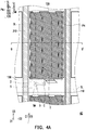
- FIG. 1A is a schematic top view of a display panel according to an embodiment of the invention.
- FIG. 1B is a schematic cross-sectional view taken along a section line AA′ in FIG. 1A .
- FIG. 1C is a schematic cross-sectional view taken along the section line AA′ in FIG. 1A .
- FIG. 2A is a schematic top view of a display panel according to another embodiment of the invention.
- FIG. 2B is a schematic cross-sectional view taken along a section line CC′ in FIG. 2A .
- FIG. 2C a schematic cross-sectional view taken along a section line DD′ in FIG. 2A .
- FIG. 3A is a schematic top view of a display panel according to still another embodiment of the invention.
- FIG. 3B is a schematic cross-sectional view taken along a section line EE′ in FIG. 2A .
- FIG. 3C a schematic cross-sectional view taken along a section line FF′ in FIG. 2A .
- FIG. 4A is a schematic top view of a display panel according to still another embodiment of the invention.
- FIG. 4B is a schematic cross-sectional view taken along a section line GG′ in FIG. 4A .
- FIG. 5 is a schematic top view of a display panel according to still another embodiment of the invention.
- FIG. 6A is a schematic top view of a display panel according to still another embodiment of the invention.
- FIG. 6B is a schematic cross-sectional view taken along a section line HH′ in FIG. 6A .
- FIG. 1A is a schematic top view of a display panel according to an embodiment of the invention.
- FIG. 1B is a schematic cross-sectional view taken along a section line AA′ in FIG. 1A .
- FIG. 1C is a schematic cross-sectional view taken along the section line AA′ in FIG. 1A .
- the number and the size of striped patterns of first polarized patterns P 1 depicted in FIG. 1A to FIG. 1C are simply illustrative and do not serve to limit the number and the size of the striped patterns provided in the invention.
- a display panel 10 includes a substrate 100 , an opposite substrate 200 , a liquid crystal layer LC, a pixel array PA, and first polarized patterns P 1 .
- a material of the substrate 100 may be glass, quartz, organic polymer, or other appropriate materials.
- the opposite substrate 200 is opposite to the substrate 100 .
- the liquid crystal layer LC is disposed between the substrate 100 and the opposite substrate 200 .
- the pixel array PA is disposed between the substrate 100 and the liquid crystal layer LC.
- the pixel array PA includes a plurality of scan lines SL, a plurality of data lines DL, a plurality of active devices TFT, a plurality of first electrodes 130 , and a plurality of second electrodes 120 .
- the scan lines SL are located on the substrate 100 .
- the data lines DL are located above the scan lines SL, and the data lines DL and the scan lines SL are staggered.
- an insulating layer 102 is sandwiched between the scan lines SL and the data lines DL.
- the extending direction D 2 of the scan lines SL is substantially perpendicular to the extending direction D 3 of the data lines DL, but the invention is not limited thereto. In other embodiments, an acute angle or an obtuse angle is included between the extending direction D 2 of the scan lines SL and the extending direction D 3 of the data lines DL.
- Each active device TFT includes a gate G, a semiconductor layer SM, a source S, and a drain D.
- the gate G is electrically connected to the scan line SL.
- the semiconductor layer SM is located above the gate G and separated from the gate G by an insulating layer.
- the source S and the drain D are disposed on the semiconductor layer SM.
- the source S is electrically connected to the data line DL.
- the active devices TFT are bottom gate thin film transistors, but the invention is not limited thereto. In other embodiments, the active devices TFT may be top gate thin film transistors or other types of switch devices.
- the pixel array PA further includes a plurality of first auxiliary electrodes 110 disposed above the data lines DL.
- the first auxiliary electrodes 110 and the data lines DL are separated from each other.
- an insulating layer 104 is sandwiched between the first auxiliary electrodes 110 and the data lines DL.
- an extending direction of the first auxiliary electrodes 110 is equal to the extending direction D 3 of the data lines DL, but the invention is not limited thereto. In other embodiments, an included angle is between the extending direction of the first auxiliary electrodes 110 and the extending direction D 3 of the data lines DL.
- the pixel array PA provided in the embodiment includes the first auxiliary electrodes 110 , it does not indicate that the first auxiliary electrodes 110 provided in the invention have to be included in the pixel array PA. In some embodiments, it is possible that the pixel array PA does not include the first auxiliary electrodes 110 and the insulating layer 104 . In some embodiments, the first auxiliary electrodes 110 serve as touch electrodes.
- the first electrodes 130 and the second electrodes 120 are located on the substrate 100 .
- the second electrodes 120 are located between the first electrodes 130 and the substrate 100 or located between the first electrodes 130 and the liquid crystal layer LC.
- the second electrodes 120 are located between the first electrodes 130 and the substrate 100 .
- An insulating layer 108 is sandwiched between the first electrodes 130 and the second electrodes 120 .
- An insulating layer 106 is sandwiched between the second electrodes 120 and the first auxiliary electrodes 110 .
- the second electrodes 120 are pixel electrodes, and the second electrodes 120 are electrically connected to the drains D of active devices TFT through contact windows C, but the invention is not limited thereto.
- the insulating layer 106 is sandwiched between the first electrodes 130 and the first auxiliary electrodes 110 , and the insulating layer 108 is sandwiched between the first electrodes 130 and the second electrodes 120 ; that is, the second electrodes 120 are disposed above the first electrodes 130 , and the second electrodes 120 are electrically connected to the drains D of active devices TFT.
- the first electrodes 130 are common electrodes, and the first electrodes 130 include a plurality of slits T. The slits T overlap with the second electrodes 120 , but the invention is not limited thereto.
- the second electrodes 120 serving as the pixel electrodes include a plurality of slits T.
- an extending direction E 1 of the slits T in a pixel region is, for example, equal to the extending direction D 3 of the data lines DL, wherein the pixel region, for example, corresponds to the location of the pixel electrodes and approximately overlaps with the pixel electrodes, but the invention is not limited thereto.
- an acute angle or an obtuse angle is included between the extending direction of the slits T in the pixel region and the extending direction D 3 of the data lines DL.
- the slits T may have another extending direction different from the extending direction E 1 at a position close to the scan lines SL, and said extending direction at the position of the slits T close to the scan lines SL may further facilitate the liquid crystal alignment.
- a portion of the first electrodes 130 is disposed above and overlaps with the data lines DL, and the portion of the first electrodes 130 has the same extending direction as that of the data lines DL.
- the first polarized patterns P 1 are disposed between the substrate 100 and the opposite substrate 200 .
- the first polarized patterns P 1 are disposed between the substrate 100 and the liquid crystal layer LC, and a color filter device CF is disposed between the liquid crystal layer LC and the opposite substrate 200 .
- a polarizing film PF and an optical compensation film CM are provided on another side of the opposite substrate 200 opposite to the color filter device CF, wherein the optical compensation film CM is disposed between the polarizing film PF and the opposite substrate 200 , but the invention is not limited thereto.
- the first polarized patterns P 1 are disposed between the color filter device CF and the liquid crystal layer LC or between the color filter device CF and the opposite substrate 200 , and the polarizing film PF and the optical compensation film CM are disposed on another side of the substrate 100 opposite to the pixel array PA, such as the outer side of the substrate 100 , wherein the optical compensation film CM is disposed between the polarizing film PF and the substrate 100 .
- the polarizing film PF is disposed on the substrate 100 or the opposite substrate 200 where no first polarized patterns P 1 are disposed, and the optical compensation film CM is disposed between the polarizing film PF and the substrate 100 or the opposite substrate 200 .
- the first polarized patterns P 1 and the first auxiliary electrodes 110 belong to the same film layer and are separated from each other. In one embodiment, the first polarized patterns P 1 and the first auxiliary electrodes 110 are, for example, separated by an insulating layer, so that there is no short circuit between the first polarized patterns P 1 and the first auxiliary electrodes 110 . In one embodiment, the first polarized patterns P 1 and the first auxiliary electrodes 110 are simultaneously formed, for example, by performing a nano-imprint process, such that no additional process for manufacturing the first polarized patterns P 1 is required, and the manufacturing costs are reduced.
- each of the first polarized patterns P 1 is composed of a plurality of striped patterns in parallel, a width W of each of the striped patterns is within a range from 15 nm to 120 nm, and a gap GP between the adjacent striped patterns is within a range from 15 nm to 120 nm.
- the first polarized patterns P 1 include a plurality of independent striped patterns extending along an extending direction E 2 , and the extending direction E 2 of the first polarized patterns P 1 is different from the extending direction E 1 of the slits T.
- an alignment film (not illustrated) is sandwiched between the liquid crystal layer LC and the substrate 100 .
- the alignment film has an alignment direction which is substantially parallel to or substantially perpendicular to an extending direction of polarized patterns (e.g., the extending direction E 2 of the first polarized patterns P 1 ).
- the liquid crystal layer LC includes positive type liquid crystal (i.e., liquid crystal with positive dielectric anisotropy), an included angle between the extending direction E 2 of the first polarized patterns P 1 and the extending direction E 1 of the slits T is ⁇ degree, ⁇ 15 ⁇ 15, and ⁇ 0. In one embodiment, an included angle between the extending direction E 2 of the first polarized patterns P 1 and the extending direction E 1 of the slits T is ⁇ degree, ⁇ 15 ⁇ 2 or 2 ⁇ 15, and in some preferred embodiments, ⁇ 15 ⁇ 5 or 5 ⁇ 15.
- positive type liquid crystal i.e., liquid crystal with positive dielectric anisotropy
- an included angle between the extending direction E 2 of the first polarized patterns P 1 and the extending direction E 1 of the slits T is ⁇ degree, ⁇ 15 ⁇ 2 or 2 ⁇ 15, and in some preferred embodiments, ⁇ 15 ⁇ 5 or 5 ⁇ 15.
- the extending direction of the first auxiliary electrodes 110 is, for example, equal to the extending direction D 3 of the data lines DL, and an included angle between the extending direction E 2 of the first polarized patterns P 1 and the extending direction of the first auxiliary electrodes 110 is less than 45 degrees.
- the liquid crystal layer LC includes negative type liquid crystal (i.e., liquid crystal with negative dielectric anisotropy), an included angle between the extending direction E 2 of the first polarized patterns P 1 and the extending direction E 1 of the slits T is ⁇ degree, 75 ⁇ 105, and ⁇ 90. In one embodiment, an included angle between the extending direction E 2 of the first polarized patterns P 1 and the extending direction E 1 of the slits T is ⁇ degree, 75 ⁇ 88 or 92 ⁇ 105, and in some preferred embodiments, 75 ⁇ 85 or 95 ⁇ 105.
- negative type liquid crystal i.e., liquid crystal with negative dielectric anisotropy
- the extending direction of the first auxiliary electrodes 110 is, for example, equal to the extending direction D 2 of the scan lines SL, and an included angle between the extending direction E 2 of the first polarized patterns P 1 and an extending direction of the first auxiliary electrodes 110 is less than 45 degrees.
- the first polarized patterns P 1 and the first auxiliary electrodes 110 are simultaneously formed, for example, by performing a nano-imprint process.
- the photomask patterns are transferred and printed by applying a physical contact method; hence, a problem of a film separation is easily generated after imprinting.
- an included angle between the extending direction E 2 of the first polarized patterns P 1 and the extending direction of the first auxiliary electrodes 110 is less than 45 degrees, and a direction of the film separation during separating the film may be as close as possible to the extending direction E 2 of the first polarized patterns P 1 and/or the extending direction of the first auxiliary electrodes 110 , such that the overall yield of the nano-imprint process may increase.
- the first polarized patterns P 1 and the first auxiliary electrodes 110 belong to the same film layer. Therefore, it is not required to form any additional polarizing film at the outer side of the substrate 100 , and the manufacturing costs of the display panel 10 may be reduced while the yield of the display panel 10 is increased.
- the extending direction E 2 of the first polarized patterns P 1 provided in the invention is different from the extending direction E 1 of the slits T in the pixel array PA. Owing to the alignment achieved by the alignment film, the display panel 10 may accomplish better polarizing effects, and the liquid crystal efficiency may be enhanced.
- FIG. 2A is a schematic top view of a display panel according to another embodiment of the invention.
- FIG. 2B is a schematic cross-sectional view taken along a section line CC′ in FIG. 2A .
- FIG. 2C a schematic cross-sectional view taken along a section line DD′ in FIG. 2A .
- the number and the size of striped patterns of first polarized patterns P 2 depicted in FIG. 2A to FIG. 2C are simply illustrative and do not serve to limit the number and the size of striped patterns provided in the invention.
- the reference numbers of components and partial content of the embodiments depicted in FIG. 1A to FIG. 1C are adopted in the embodiments depicted in FIG. 2A to FIG. 2C , wherein identical or similar reference numbers indicate identical or similar components, and descriptions of the same techniques are omitted. The omitted descriptions may be found in the above embodiments and will not be repeated in the following embodiments.
- the main difference between the embodiment depicted in FIG. 2A to FIG. 2C and the embodiment depicted in FIG. 1A to FIG. 1C lies in that the first polarized patterns P 1 shown in FIG. 1A to FIG. 1C and the first auxiliary electrodes 110 belong to the same film layer, while the first polarized patterns P 2 shown in FIG. 2A to FIG. 2C and the data lines DL belong to the same film layer.
- a display panel 20 includes a substrate 100 , an opposite substrate 200 , a liquid crystal layer LC, a pixel array PA, and first polarized patterns P 2 .
- the opposite substrate 200 is opposite to the substrate 100 .
- the liquid crystal layer LC is located between the substrate 100 and the opposite substrate 200 .
- the pixel array PA is located between the substrate 100 and the liquid crystal layer LC.
- the pixel array PA includes a plurality of scan lines SL, a plurality of data lines DL, a plurality of active devices TFT, a plurality of first electrodes 130 , and a plurality of second electrodes 120 .
- the data lines DL and the scan lines SL are staggered.
- the active devices TFT are electrically connected to the scan lines SL and the data lines DL.
- the second electrodes 120 are electrically connected to the active devices TFT.
- the first electrodes 130 are located on the substrate 100 .
- Each of the first electrodes 130 includes a plurality of slits T.
- the first polarized patterns P 2 in a direction D 1 perpendicular to the substrate 100 overlap with the second electrodes 120 and partially overlap with the first electrodes 130 .
- the first polarized patterns P 2 are located between the substrate 100 and the opposite substrate 200 .
- the extending direction E 3 of the first polarized patterns P 2 is different from the extending direction E 1 of the slits T.
- the first polarized patterns P 2 and the data lines DL belong to the same film layer and are separated from each other, and an included angle between the extending direction E 3 of the first polarized patterns P 2 and the extending direction D 3 of the data lines DL is less than 45 degrees.
- the first polarized patterns P 2 and the data lines DL are simultaneously formed by, for example, performing an etching and photolithography process or the nano-imprint process, such that no additional process for manufacturing the first polarized patterns P 2 is required.
- the photomask patterns are transferred and printed by applying a physical contact method; hence, a problem of a film separation is easily generated after imprinting.
- an included angle between the extending direction E 3 of the first polarized patterns P 2 and the extending direction D 3 of the data lines DL is less than 45 degrees, and a direction of the film separation during separating the film may be as close as possible to the extending direction E 3 of the first polarized patterns P 2 and/or the extending direction D 3 of the data lines DL, such that the overall yield of the nano-imprint process may increase.
- the first polarized patterns P 2 and the data lines DL belong to the same film layer. Therefore, it is not required to form any additional polarizing film at the outer side of the substrate 100 , and the manufacturing costs of the display panel 20 may be reduced while the yield of the display panel 20 is increased.
- the extending direction E 3 of the first polarized patterns P 2 provided in the invention is different from the extending direction E 1 of the slits T of the first electrodes 130 in the pixel array PA. Owing to the alignment achieved by the alignment film, the display panel 20 may accomplish better polarizing effects, and the liquid crystal efficiency may be enhanced.
- FIG. 3A is a schematic top view of a display panel according to another embodiment of the invention.
- FIG. 3B is a schematic cross-sectional view taken along a section line EE′ in FIG. 3A .
- FIG. 3C a schematic cross-sectional view taken along a section line FF′ in FIG. 3A .
- the number and the size of striped patterns of the first polarized patterns P 3 depicted in FIG. 3A to FIG. 3C are simply illustrative and do not serve to limit the number and the size of striped patterns provided in the invention.
- the main difference between the embodiment depicted in FIG. 3A to FIG. 3C and the embodiment depicted in FIG. 1A to FIG. 1C lies in that the first polarized patterns P 1 shown in FIG. 1A to FIG. 1C and the first auxiliary electrodes 110 belong to the same film layer, while the first polarized patterns P 3 shown in FIG. 3A to FIG. 3C and the scan lines SL belong to the same film layer.
- a display panel 30 includes a substrate 100 , an opposite substrate 200 , a liquid crystal layer LC, a pixel array PA, and first polarized patterns P 3 .
- the opposite substrate 200 is opposite to the substrate 100 .
- the liquid crystal layer LC is located between the substrate 100 and the opposite substrate 200 .
- the pixel array PA is located between the substrate 100 and the liquid crystal layer LC.
- the pixel array PA includes a plurality of scan lines SL, a plurality of data lines DL, a plurality of active devices TFT, a plurality of first electrodes 130 , and a plurality of second electrodes 120 .
- the data lines DL and the scan lines SL are staggered.
- the active devices TFT are electrically connected to the scan lines SL and the data lines DL.
- the second electrodes 120 are electrically connected to the active devices TFT.
- the first electrodes 130 are located on the substrate 100 .
- Each of the first electrodes 130 includes a plurality of slits T.
- the first polarized patterns P 3 in a direction D 1 perpendicular to the substrate 100 overlap with the second electrodes 120 and partially overlap with the first electrodes 130 .
- the first polarized patterns P 3 are located between the substrate 100 and the opposite substrate 200 .
- the extending direction E 4 of the first polarized patterns P 3 is different from the extending direction E 1 of the slits T.
- the liquid crystal layer LC includes negative type liquid crystal, an included angle between an extending direction E 4 of the first polarized patterns P 3 and an extending direction E 1 of the slits T is ⁇ degree, 75 ⁇ 105, and ⁇ 90. In an embodiment, an included angle between the extending direction E 4 of the first polarized patterns P 3 and the extending direction E 1 of the slits T is ⁇ degree, 75 ⁇ 88 or 92 ⁇ 105, and in some preferred embodiments, 75 ⁇ 85 or 95 ⁇ 105.
- the first polarized patterns P 3 and the scan lines SL belong to the same film layer and are separated from each other, and an included angle between the extending direction E 4 of the first polarized patterns P 3 and the extending direction D 2 of the scan lines SL is less than 45 degrees.
- the first polarized patterns P 3 and the scan lines SL are simultaneously formed by, for example, performing an etching and photolithography process or the nano-imprint process, such that no additional process for manufacturing the first polarized patterns P 3 is required.
- the nano-imprint process the photomask patterns transferred and printed by applying the physical contact method; hence, a problem of a film separation is easily generated after imprinting.
- an included angle between the extending direction E 4 of the first polarized patterns P 3 and the extending direction D 2 of the scan lines SL is less than 45 degrees, and a direction of the film separation during separating the film may be as close as possible to the extending direction E 4 of the first polarized patterns P 3 and/or the extending direction D 2 of the scan lines SL, such that the overall yield of the nano-imprint process may increase.
- the first polarized patterns P 3 and the scan lines SL belong to the same film layer. Therefore, it is not required to form any additional polarizing film at the outer side of the substrate 100 , and the manufacturing costs of the display panel 30 may be reduced while the yield of the display panel 30 is increased.
- the extending direction E 4 of the first polarized patterns P 3 provided in the invention is different from the extending direction E 1 of the slits T of the first electrodes 130 in the pixel array PA. Owing to the alignment of the alignment film, the display panel 30 may achieve better polarizing effects, and the liquid crystal efficiency may be enhanced.
- FIG. 4A is a schematic cross-sectional view of a display panel according to yet another embodiment of the invention.
- FIG. 4B is a schematic cross-sectional view taken along a section line GG′ in FIG. 4A . It should be noted that the number and the size of striped patterns of the first polarized patterns P 4 depicted in FIG. 4A and FIG. 4 B are simply illustrative and do not serve to limit the number and the size of striped patterns provided in the invention.
- the main difference between the embodiment depicted in FIG. 4A and FIG. 4B and the embodiment depicted in FIG. 1A to FIG. 1C lies in that the first polarized patterns P 1 in FIG. 1A to FIG. 1C are located between the liquid crystal layer and the substrate 100 , while the first polarized patterns P 4 in FIG. 4A and FIG. 4B are located between the liquid crystal layer LC and the opposite substrate 200 .
- a display panel 40 includes a substrate 100 , an opposite substrate 200 , a liquid crystal layer LC, a pixel array PA, and first polarized patterns P 4 .
- the opposite substrate 200 is opposite to the substrate 100 .
- the liquid crystal layer LC is located between the substrate 100 and the opposite substrate 200 .
- the pixel array PA is located between the substrate 100 and the liquid crystal layer LC.
- the pixel array PA includes a plurality of scan lines SL, a plurality of data lines DL, a plurality of active devices TFT, a plurality of first electrodes 130 , and a plurality of second electrodes 120 .
- the data lines DL and the scan lines SL are staggered.
- the active devices TFT are electrically connected to the scan lines SL and the data lines DL.
- the second electrodes 120 are electrically connected to the active devices TFT.
- the first electrodes 130 are located on the substrate 100 . Each of the first electrodes 130 includes a plurality of slits T.
- the first polarized patterns P 4 are disposed between the liquid crystal layer LC and the opposite substrate 200 .
- the extending direction E 5 of the first polarized patterns P 4 is different from the extending direction E 1 of the slits T.
- An included angle between the extending direction E 5 of the first polarized patterns P 4 and the extending direction E 1 of the slits T is ⁇ degree, and the value of ⁇ is preferably the value described in the above embodiments.
- Plural second auxiliary electrodes 210 are located on the opposite substrate 200 .
- an extending direction of the second auxiliary electrodes 210 is identical to the extending direction D 3 of the data lines DL, but the invention is not limited thereto.
- the extending direction of the second auxiliary electrodes 210 is identical to the extending direction D 2 of the scan lines SL.
- the first polarized patterns P 4 and the second auxiliary electrodes 210 belong to the same film layer, and an included angle between the extending direction E 5 of the first polarized patterns P 4 and the extending direction of the second auxiliary electrodes 210 is less than 45 degrees.
- the pixel array PA even includes a plurality of first auxiliary electrodes 110 located above the scan lines SL.
- the first auxiliary electrodes 110 and the scan lines SL are separated at least by an insulating layer 102 from each other.
- an extending direction of the first auxiliary electrodes 110 is equal to the extending direction D 2 of the scan lines SL.
- the second auxiliary electrodes 210 and the first auxiliary electrodes 110 may serve as touch electrodes.
- the extending direction of the first auxiliary electrodes 110 is substantially perpendicular to the extending direction of the second auxiliary electrodes 210 .
- the second auxiliary electrodes 210 may serve as view-angle control signal electrodes.
- the second auxiliary electrodes 210 are located between the color filter device CF and the opposite substrate 200 , and an insulating layer 202 is sandwiched between the second auxiliary electrodes 210 and the color filter device CF, but the invention is not limited thereto. In other embodiments, the color filter device CF is located between the second auxiliary electrodes 210 and the opposite substrate 200 .
- the color filter device CF is disposed on the opposite substrate 200 .
- the invention is not limited thereto.
- the color filter device CF may also be disposed on the substrate 100 to form a color filter on array (COA) structure.
- COA color filter on array
- the optical compensation film CM is arranged at another side of the substrate 100 opposite to the pixel array PA. In one embodiment, the optical compensation film CM is located between the polarizing film PF and the substrate 100 , but the invention is not limited thereto. In other embodiments, no polarizing film PF is arranged on the substrate 100 , and plural second polarized patterns are provided between the substrate 100 and the liquid crystal layer LC. In one embodiment, the second polarized patterns and the scan lines, the data lines, or the first auxiliary electrodes belong to the same film layer and are, for example, simultaneously formed together with the scan lines, the data lines, or the first auxiliary electrodes by performing the nano-imprint process.
- the second polarized patterns are located on the substrate 100 or the opposite substrate 200 where no first polarized pattern is located, and the second polarized patterns overlap with the first polarized patterns P 4 in a direction D 1 perpendicular to the substrate 100 .
- the extending direction of the second polarized patterns is perpendicular to the extending direction of the first polarized patterns P 4 .
- the first polarized patterns P 4 and the second auxiliary electrodes 210 belong to the same film layer. Therefore, it is not required to form any additional polarizing film at the outer side of the opposite substrate 200 , and the manufacturing costs of the display panel 40 may be reduced while the yield of the display panel 40 is increased.
- the extending direction of the first polarized patterns P 4 provided in the invention is different from the extending direction of the slits of the first electrodes in the pixel array. Owing to the alignment achieved by the alignment film, the display panel 40 may accomplish better polarizing effects, and the liquid crystal efficiency may be enhanced.
- FIG. 5 is a schematic cross-sectional view of a display panel according to yet another embodiment of the invention. It should be noted that the number and the size of striped patterns of the first polarized patterns P 4 depicted in FIG. 5 are simply illustrative and do not serve to limit the number and the size of striped patterns provided in the invention.
- the main difference between the embodiment depicted in FIG. 4A and FIG. 4B and the embodiment depicted in FIG. 5 lies in that the first polarized patterns P 4 depicted in FIG. 4B and the second auxiliary electrodes 210 are located between the color filter device CF and the opposite substrate 200 , and the first polarized patterns P 4 depicted in FIG. 5 and the second auxiliary electrodes 210 are located between the liquid crystal layer LC and the color filter device CF.
- a display panel 50 includes a substrate 100 , an opposite substrate 200 , a liquid crystal layer LC, a pixel array PA, and first polarized patterns P 4 .
- the opposite substrate 200 is located opposite to the substrate 100 .
- the liquid crystal layer LC is located between the substrate 100 and the opposite substrate 200 .
- the pixel array PA is located between the substrate 100 and the liquid crystal layer LC.
- the pixel array PA includes a plurality of scan lines, a plurality of data lines DL, a plurality of active devices, a plurality of first electrodes 130 , and a plurality of second electrodes 120 .
- the data lines DL and the scan lines are staggered.
- the active devices are electrically connected to the scan lines SL and the data lines DL, and the second electrodes 120 are electrically connected to the active devices.
- the first electrodes 130 are disposed on the substrate 100 .
- Each of the first electrodes 130 includes a plurality of slits.
- the first polarized patterns P 4 in a direction D 1 perpendicular to the substrate 100 overlap with the second electrodes 120 and partially overlap with the first electrodes 130 .
- the first polarized patterns P 4 are located between the liquid crystal layer LC and the opposite substrate 200 .
- the extending direction of the first polarized patterns P 4 is different from the extending direction of the slits.
- the first polarized patterns P 4 and the second auxiliary electrodes 210 belong to the same film layer. Therefore, it is not required to form any additional polarizing film at the outer side of the opposite substrate 200 , and the manufacturing costs of the display panel 50 may be reduced while the yield of the display panel 50 is increased.
- the extending direction of the first polarized patterns P 4 provided in the invention is different from the extending direction of the slits of the first electrodes 130 in the pixel array PA, which contributes to the smooth movement of the liquid crystal in the liquid crystal layer LC along a predetermined direction.
- FIG. 6A is a schematic top view of a display panel 60 according to yet another embodiment of the invention.
- FIG. 6B is a schematic cross-sectional view taken along a section line HH′ in FIG. 6A . It should be noted that the number and the size of striped patterns of the first polarized patterns P 4 and the second polarized patterns P 5 depicted in FIG. 6A and FIG. 6B are simply illustrative and do not serve to limit the number and the size of striped patterns provided in the invention.
- the main difference between the embodiment depicted in FIG. 4A and FIG. 4B and the embodiment depicted in FIG. 6A and FIG. 6B lies in that there are plural second polarized patterns P 5 between the substrate 100 and the liquid crystal layer LC.
- the second polarized patterns P 5 and the first auxiliary electrodes 110 belong to the same film layer, but the invention is not limited thereto. In other embodiments, the second polarized patterns P 5 and the scan lines SL or the data lines DL belong to the same film layer.
- the second polarized patterns P 5 in a direction D 1 perpendicular to the substrate 100 overlap with the first polarized patterns P 4 , wherein the extending direction E 6 of the second polarized patterns P 5 intersects with the extending direction E 5 of the first polarized patterns P 4 .
- the extending direction E 6 of the second polarized patterns P 5 is perpendicular to the extending direction E 5 of the first polarized patterns P 4 .
- an optical compensation film may be arranged at an outer side of the substrate 100 or the opposite substrate 200 , but the invention is not limited thereto.
- the second polarized patterns P 5 are arranged between the substrate 100 and the liquid crystal layer LC
- the first polarized patterns P 4 are arranged between the opposite substrate 200 and the liquid crystal layer LC; therefore, no additional polarizing film is required to be disposed at the outer side of the substrate 100 and the opposite substrate 200 .
- the first polarized patterns are located between the substrate and the opposite substrate. Therefore, it is not required to form any additional polarizing film at the outer side of the substrate and/or the opposite substrate, and the manufacturing costs of the display panel may be reduced while the yield of the display panel is increased.
- the extending direction of the first polarized patterns provided in the invention is different from the extending direction of the slits in the pixel array. Owing to the alignment achieved by the alignment film, the display panel may accomplish better polarizing effects, and the liquid crystal efficiency is enhanced.
Landscapes
- Physics & Mathematics (AREA)
- Nonlinear Science (AREA)
- General Physics & Mathematics (AREA)
- Crystallography & Structural Chemistry (AREA)
- Optics & Photonics (AREA)
- Chemical & Material Sciences (AREA)
- Engineering & Computer Science (AREA)
- Mathematical Physics (AREA)
- Theoretical Computer Science (AREA)
- General Engineering & Computer Science (AREA)
- Geometry (AREA)
- Microelectronics & Electronic Packaging (AREA)
- Human Computer Interaction (AREA)
- Spectroscopy & Molecular Physics (AREA)
- Liquid Crystal (AREA)
Applications Claiming Priority (3)
| Application Number | Priority Date | Filing Date | Title |
|---|---|---|---|
| TW106130949A | 2017-09-11 | ||
| TW106130949A TWI636566B (zh) | 2017-09-11 | 2017-09-11 | 顯示面板 |
| TW106130949 | 2017-09-11 |
Publications (2)
| Publication Number | Publication Date |
|---|---|
| US20190079346A1 US20190079346A1 (en) | 2019-03-14 |
| US10809561B2 true US10809561B2 (en) | 2020-10-20 |
Family
ID=61215380
Family Applications (1)
| Application Number | Title | Priority Date | Filing Date |
|---|---|---|---|
| US16/033,248 Active 2038-08-01 US10809561B2 (en) | 2017-09-11 | 2018-07-12 | Display panel |
Country Status (3)
| Country | Link |
|---|---|
| US (1) | US10809561B2 (zh) |
| CN (1) | CN107728397B (zh) |
| TW (1) | TWI636566B (zh) |
Families Citing this family (4)
| Publication number | Priority date | Publication date | Assignee | Title |
|---|---|---|---|---|
| TWI647525B (zh) * | 2018-03-05 | 2019-01-11 | 友達光電股份有限公司 | 畫素結構 |
| TWI700535B (zh) * | 2019-07-03 | 2020-08-01 | 友達光電股份有限公司 | 畫素陣列基板 |
| TWI746185B (zh) * | 2020-09-25 | 2021-11-11 | 凌巨科技股份有限公司 | 液晶顯示裝置 |
| TWI740747B (zh) * | 2020-12-14 | 2021-09-21 | 友達光電股份有限公司 | 液晶面板 |
Citations (11)
| Publication number | Priority date | Publication date | Assignee | Title |
|---|---|---|---|---|
| US6396553B1 (en) * | 1998-06-16 | 2002-05-28 | Nec Corporation | Twisted nematic liquid crystal display device with improved viewing angle characteristics |
| CN1658035A (zh) | 2004-02-18 | 2005-08-24 | 力特光电科技股份有限公司 | 广视角液晶显示面板 |
| US8081273B2 (en) | 2006-10-26 | 2011-12-20 | Samsung Electronics Co., Ltd. | Liquid crystal display |
| US20120057106A1 (en) * | 2010-09-07 | 2012-03-08 | Electronics And Telecommunications Research Institute | Polarizer and liquid crystal display |
| US20140049736A1 (en) * | 2012-08-20 | 2014-02-20 | Beijing Boe Optoelectronics Technology Co., Ltd. | Liquid crystal display panel, method for fabricating the same and liquid crystal display device |
| CN104330915A (zh) | 2014-11-07 | 2015-02-04 | 京东方科技集团股份有限公司 | 一种阵列基板、液晶显示面板及显示装置 |
| CN105652504A (zh) | 2016-04-11 | 2016-06-08 | 京东方科技集团股份有限公司 | 彩膜基板及其制作方法、显示装置 |
| CN106154655A (zh) | 2016-08-26 | 2016-11-23 | 京东方科技集团股份有限公司 | 一种阵列基板及其制造方法、显示装置及驱动方法 |
| CN107121719A (zh) | 2017-07-03 | 2017-09-01 | 京东方科技集团股份有限公司 | 一种线栅偏振片、显示装置及线栅偏振片的制备方法 |
| US20180130929A1 (en) * | 2016-11-09 | 2018-05-10 | Samsung Display Co. Ltd. | Display device and method for fabricating the same |
| US20180181240A1 (en) * | 2016-12-26 | 2018-06-28 | Lg Display Co., Ltd. | Display Device with Integrated Touch Screen |
Family Cites Families (16)
| Publication number | Priority date | Publication date | Assignee | Title |
|---|---|---|---|---|
| TW583425B (en) * | 2001-08-02 | 2004-04-11 | Sanyo Electric Co | Liquid crystal display |
| KR100872562B1 (ko) * | 2002-12-31 | 2008-12-08 | 하이디스 테크놀로지 주식회사 | 액정표시장치 |
| CN1945396B (zh) * | 2005-10-09 | 2012-08-29 | 财团法人工业技术研究院 | 液晶显示面板 |
| JP2008282001A (ja) * | 2007-04-10 | 2008-11-20 | Fujifilm Corp | マトリクス型液晶表示装置 |
| CN101290446B (zh) * | 2008-05-16 | 2011-10-05 | 京东方科技集团股份有限公司 | Tft-lcd阵列基板及其制造方法 |
| KR101002594B1 (ko) * | 2008-11-06 | 2010-12-20 | 웅진케미칼 주식회사 | 편광특성이 내재된 유연한 기판 및 그를 구비한 유연한 박막 액정 표시 장치 |
| EP2400341B1 (en) * | 2009-02-17 | 2014-12-03 | Sharp Kabushiki Kaisha | Liquid crystal display device |
| KR20120040870A (ko) * | 2010-10-20 | 2012-04-30 | 엘지이노텍 주식회사 | 액정표시장치 |
| EP2487529B1 (en) * | 2011-02-14 | 2014-05-21 | Samsung Electronics Co., Ltd. | Display panel comprising metal grid color selective polarizer |
| CN104991377B (zh) * | 2015-08-03 | 2018-01-30 | 京东方科技集团股份有限公司 | 阵列基板、液晶显示面板及显示装置 |
| CN105785665A (zh) * | 2016-05-09 | 2016-07-20 | 深圳市华星光电技术有限公司 | Lcd显示器 |
| TWI575287B (zh) * | 2016-06-22 | 2017-03-21 | 友達光電股份有限公司 | 顯示面板及顯示模組 |
| CN105929593A (zh) * | 2016-07-11 | 2016-09-07 | 京东方科技集团股份有限公司 | 阵列基板、透明显示基板和透明显示装置 |
| CN106019692B (zh) * | 2016-07-28 | 2019-08-30 | 京东方科技集团股份有限公司 | 一种显示基板、显示装置及制作方法 |
| CN106597730A (zh) * | 2016-12-27 | 2017-04-26 | 深圳市华星光电技术有限公司 | 液晶显示面板及液晶显示器 |
| CN106950636A (zh) * | 2017-04-20 | 2017-07-14 | 京东方科技集团股份有限公司 | 一种金属线栅偏振片基板及其制备方法 |
-
2017
- 2017-09-11 TW TW106130949A patent/TWI636566B/zh active
- 2017-11-14 CN CN201711120002.4A patent/CN107728397B/zh active Active
-
2018
- 2018-07-12 US US16/033,248 patent/US10809561B2/en active Active
Patent Citations (12)
| Publication number | Priority date | Publication date | Assignee | Title |
|---|---|---|---|---|
| US6396553B1 (en) * | 1998-06-16 | 2002-05-28 | Nec Corporation | Twisted nematic liquid crystal display device with improved viewing angle characteristics |
| CN1658035A (zh) | 2004-02-18 | 2005-08-24 | 力特光电科技股份有限公司 | 广视角液晶显示面板 |
| US8081273B2 (en) | 2006-10-26 | 2011-12-20 | Samsung Electronics Co., Ltd. | Liquid crystal display |
| US20120057106A1 (en) * | 2010-09-07 | 2012-03-08 | Electronics And Telecommunications Research Institute | Polarizer and liquid crystal display |
| US20140049736A1 (en) * | 2012-08-20 | 2014-02-20 | Beijing Boe Optoelectronics Technology Co., Ltd. | Liquid crystal display panel, method for fabricating the same and liquid crystal display device |
| CN104330915A (zh) | 2014-11-07 | 2015-02-04 | 京东方科技集团股份有限公司 | 一种阵列基板、液晶显示面板及显示装置 |
| US9880414B2 (en) | 2014-11-07 | 2018-01-30 | Boe Technology Group Co., Ltd. | Array substrate, liquid crystal display panel and display device |
| CN105652504A (zh) | 2016-04-11 | 2016-06-08 | 京东方科技集团股份有限公司 | 彩膜基板及其制作方法、显示装置 |
| CN106154655A (zh) | 2016-08-26 | 2016-11-23 | 京东方科技集团股份有限公司 | 一种阵列基板及其制造方法、显示装置及驱动方法 |
| US20180130929A1 (en) * | 2016-11-09 | 2018-05-10 | Samsung Display Co. Ltd. | Display device and method for fabricating the same |
| US20180181240A1 (en) * | 2016-12-26 | 2018-06-28 | Lg Display Co., Ltd. | Display Device with Integrated Touch Screen |
| CN107121719A (zh) | 2017-07-03 | 2017-09-01 | 京东方科技集团股份有限公司 | 一种线栅偏振片、显示装置及线栅偏振片的制备方法 |
Also Published As
| Publication number | Publication date |
|---|---|
| CN107728397A (zh) | 2018-02-23 |
| TWI636566B (zh) | 2018-09-21 |
| US20190079346A1 (en) | 2019-03-14 |
| CN107728397B (zh) | 2021-04-09 |
| TW201913999A (zh) | 2019-04-01 |
Similar Documents
| Publication | Publication Date | Title |
|---|---|---|
| US10809561B2 (en) | Display panel | |
| KR101978326B1 (ko) | 어레이 기판, 그 제조 방법 및 구동 방법, 및 디스플레이 디바이스 | |
| US8174636B2 (en) | Thin film transistor substrate and liquid crystal display having the same comprising a coupling capacitor as a voltage divider between a TFT and a data line | |
| US8455870B2 (en) | Thin film transistor array panel and method of manufacturing the same | |
| US8908116B2 (en) | Liquid crystal display device | |
| US9442236B2 (en) | Liquid crystal display including wire grid polarizer and manufacturing method thereof | |
| US8085375B2 (en) | Liquid crystal display and method of manufacturing the same | |
| US7859629B2 (en) | In-plane switching mode liquid crystal display wherein the upper and lower pixel electrodes are arranged on opposite sides of the respective upper and lower pixel regions | |
| US20170199410A1 (en) | Array substrate, method of manufacturing the same, and liquid crystal display panel | |
| US10310339B2 (en) | Liquid crystal display device and method for manufacturing the same | |
| US20150092132A1 (en) | Thin film transistor array panel, liquid crystal display and manufacturing method of thin film transistor array panel | |
| US10353251B2 (en) | Display panel and manufacturing method thereof | |
| US8502945B2 (en) | Array substrate of fringe field switching mode liquid crystal display panel and method of manufacturing the same | |
| US9853060B2 (en) | Thin film transistor substrate and method of manufacturing the same | |
| KR20040034189A (ko) | 액정표시장치용 어레이 기판 및 그 제조방법 | |
| EP3279721B1 (en) | Array substrate and manufacturing method therefor, and display device | |
| US9690146B2 (en) | Array substrate, its manufacturing method, and display device | |
| JP5139503B2 (ja) | 液晶表示装置およびその製造方法 | |
| US9436042B2 (en) | Liquid crystal display device including first to third wirings and a pixel electrode, and method of manufacturing the same | |
| US8841679B2 (en) | Thin film transistor array panel | |
| WO2017128779A1 (zh) | 显示基板及其制作方法、显示装置 | |
| US10816857B2 (en) | Display device | |
| US10180610B2 (en) | Thin film transistor array substrate and manufacturing method thereof, and display device | |
| KR102244437B1 (ko) | 액정 표시장치 및 그 제조방법 | |
| JP6625307B1 (ja) | 液晶表示装置及び液晶表示装置の製造方法 |
Legal Events
| Date | Code | Title | Description |
|---|---|---|---|
| AS | Assignment |
Owner name: AU OPTRONICS CORPORATION, TAIWAN Free format text: ASSIGNMENT OF ASSIGNORS INTEREST;ASSIGNORS:LO, YEN-HUA;HUANG, HSIN-CHUN;GUO, WEN-REI;AND OTHERS;REEL/FRAME:046338/0863 Effective date: 20180706 |
|
| FEPP | Fee payment procedure |
Free format text: ENTITY STATUS SET TO UNDISCOUNTED (ORIGINAL EVENT CODE: BIG.); ENTITY STATUS OF PATENT OWNER: LARGE ENTITY |
|
| STPP | Information on status: patent application and granting procedure in general |
Free format text: DOCKETED NEW CASE - READY FOR EXAMINATION |
|
| STPP | Information on status: patent application and granting procedure in general |
Free format text: NON FINAL ACTION MAILED |
|
| STPP | Information on status: patent application and granting procedure in general |
Free format text: RESPONSE TO NON-FINAL OFFICE ACTION ENTERED AND FORWARDED TO EXAMINER |
|
| STPP | Information on status: patent application and granting procedure in general |
Free format text: FINAL REJECTION MAILED |
|
| STPP | Information on status: patent application and granting procedure in general |
Free format text: PUBLICATIONS -- ISSUE FEE PAYMENT RECEIVED |
|
| STCF | Information on status: patent grant |
Free format text: PATENTED CASE |
|
| MAFP | Maintenance fee payment |
Free format text: PAYMENT OF MAINTENANCE FEE, 4TH YEAR, LARGE ENTITY (ORIGINAL EVENT CODE: M1551); ENTITY STATUS OF PATENT OWNER: LARGE ENTITY Year of fee payment: 4 |