US10782003B2 - LED substrate and light illuminating apparatus with the same - Google Patents
LED substrate and light illuminating apparatus with the same Download PDFInfo
- Publication number
- US10782003B2 US10782003B2 US15/464,707 US201715464707A US10782003B2 US 10782003 B2 US10782003 B2 US 10782003B2 US 201715464707 A US201715464707 A US 201715464707A US 10782003 B2 US10782003 B2 US 10782003B2
- Authority
- US
- United States
- Prior art keywords
- led substrate
- led
- electrode
- circuit
- circuits
- Prior art date
- Legal status (The legal status is an assumption and is not a legal conclusion. Google has not performed a legal analysis and makes no representation as to the accuracy of the status listed.)
- Active, expires
Links
- 239000000758 substrate Substances 0.000 title claims abstract description 338
- 238000010586 diagram Methods 0.000 description 39
- 238000010276 construction Methods 0.000 description 31
- RYGMFSIKBFXOCR-UHFFFAOYSA-N Copper Chemical compound [Cu] RYGMFSIKBFXOCR-UHFFFAOYSA-N 0.000 description 7
- 229910052802 copper Inorganic materials 0.000 description 7
- 239000010949 copper Substances 0.000 description 7
- 229910052751 metal Inorganic materials 0.000 description 7
- 239000002184 metal Substances 0.000 description 7
- 230000000712 assembly Effects 0.000 description 6
- 238000000429 assembly Methods 0.000 description 6
- 239000011347 resin Substances 0.000 description 6
- 229920005989 resin Polymers 0.000 description 6
- 238000012423 maintenance Methods 0.000 description 4
- 239000000853 adhesive Substances 0.000 description 3
- 230000001070 adhesive effect Effects 0.000 description 3
- 238000007645 offset printing Methods 0.000 description 3
- 238000004080 punching Methods 0.000 description 3
- 238000011144 upstream manufacturing Methods 0.000 description 3
- 238000013461 design Methods 0.000 description 2
- 238000005401 electroluminescence Methods 0.000 description 2
- 238000004519 manufacturing process Methods 0.000 description 2
- 229910052782 aluminium Inorganic materials 0.000 description 1
- XAGFODPZIPBFFR-UHFFFAOYSA-N aluminium Chemical compound [Al] XAGFODPZIPBFFR-UHFFFAOYSA-N 0.000 description 1
- 238000013459 approach Methods 0.000 description 1
- 230000006835 compression Effects 0.000 description 1
- 238000007906 compression Methods 0.000 description 1
- PMHQVHHXPFUNSP-UHFFFAOYSA-M copper(1+);methylsulfanylmethane;bromide Chemical compound Br[Cu].CSC PMHQVHHXPFUNSP-UHFFFAOYSA-M 0.000 description 1
- 230000000694 effects Effects 0.000 description 1
- 238000005516 engineering process Methods 0.000 description 1
- 238000002474 experimental method Methods 0.000 description 1
- 239000004519 grease Substances 0.000 description 1
- 238000005286 illumination Methods 0.000 description 1
- 239000004973 liquid crystal related substance Substances 0.000 description 1
- 239000000463 material Substances 0.000 description 1
- QSHDDOUJBYECFT-UHFFFAOYSA-N mercury Chemical compound [Hg] QSHDDOUJBYECFT-UHFFFAOYSA-N 0.000 description 1
- 229910052753 mercury Inorganic materials 0.000 description 1
- VSQYNPJPULBZKU-UHFFFAOYSA-N mercury xenon Chemical compound [Xe].[Hg] VSQYNPJPULBZKU-UHFFFAOYSA-N 0.000 description 1
- 238000012986 modification Methods 0.000 description 1
- 230000004048 modification Effects 0.000 description 1
- 230000005855 radiation Effects 0.000 description 1
- 239000004065 semiconductor Substances 0.000 description 1
Images


Classifications
-
- F—MECHANICAL ENGINEERING; LIGHTING; HEATING; WEAPONS; BLASTING
- F21—LIGHTING
- F21V—FUNCTIONAL FEATURES OR DETAILS OF LIGHTING DEVICES OR SYSTEMS THEREOF; STRUCTURAL COMBINATIONS OF LIGHTING DEVICES WITH OTHER ARTICLES, NOT OTHERWISE PROVIDED FOR
- F21V19/00—Fastening of light sources or lamp holders
- F21V19/001—Fastening of light sources or lamp holders the light sources being semiconductors devices, e.g. LEDs
- F21V19/0015—Fastening arrangements intended to retain light sources
- F21V19/0025—Fastening arrangements intended to retain light sources the fastening means engaging the conductors of the light source, i.e. providing simultaneous fastening of the light sources and their electric connections
-
- F—MECHANICAL ENGINEERING; LIGHTING; HEATING; WEAPONS; BLASTING
- F21—LIGHTING
- F21K—NON-ELECTRIC LIGHT SOURCES USING LUMINESCENCE; LIGHT SOURCES USING ELECTROCHEMILUMINESCENCE; LIGHT SOURCES USING CHARGES OF COMBUSTIBLE MATERIAL; LIGHT SOURCES USING SEMICONDUCTOR DEVICES AS LIGHT-GENERATING ELEMENTS; LIGHT SOURCES NOT OTHERWISE PROVIDED FOR
- F21K9/00—Light sources using semiconductor devices as light-generating elements, e.g. using light-emitting diodes [LED] or lasers
- F21K9/20—Light sources comprising attachment means
-
- F—MECHANICAL ENGINEERING; LIGHTING; HEATING; WEAPONS; BLASTING
- F21—LIGHTING
- F21V—FUNCTIONAL FEATURES OR DETAILS OF LIGHTING DEVICES OR SYSTEMS THEREOF; STRUCTURAL COMBINATIONS OF LIGHTING DEVICES WITH OTHER ARTICLES, NOT OTHERWISE PROVIDED FOR
- F21V17/00—Fastening of component parts of lighting devices, e.g. shades, globes, refractors, reflectors, filters, screens, grids or protective cages
- F21V17/10—Fastening of component parts of lighting devices, e.g. shades, globes, refractors, reflectors, filters, screens, grids or protective cages characterised by specific fastening means or way of fastening
-
- F—MECHANICAL ENGINEERING; LIGHTING; HEATING; WEAPONS; BLASTING
- F21—LIGHTING
- F21V—FUNCTIONAL FEATURES OR DETAILS OF LIGHTING DEVICES OR SYSTEMS THEREOF; STRUCTURAL COMBINATIONS OF LIGHTING DEVICES WITH OTHER ARTICLES, NOT OTHERWISE PROVIDED FOR
- F21V19/00—Fastening of light sources or lamp holders
- F21V19/001—Fastening of light sources or lamp holders the light sources being semiconductors devices, e.g. LEDs
- F21V19/003—Fastening of light source holders, e.g. of circuit boards or substrates holding light sources
-
- F—MECHANICAL ENGINEERING; LIGHTING; HEATING; WEAPONS; BLASTING
- F21—LIGHTING
- F21V—FUNCTIONAL FEATURES OR DETAILS OF LIGHTING DEVICES OR SYSTEMS THEREOF; STRUCTURAL COMBINATIONS OF LIGHTING DEVICES WITH OTHER ARTICLES, NOT OTHERWISE PROVIDED FOR
- F21V23/00—Arrangement of electric circuit elements in or on lighting devices
- F21V23/06—Arrangement of electric circuit elements in or on lighting devices the elements being coupling devices, e.g. connectors
-
- F—MECHANICAL ENGINEERING; LIGHTING; HEATING; WEAPONS; BLASTING
- F21—LIGHTING
- F21V—FUNCTIONAL FEATURES OR DETAILS OF LIGHTING DEVICES OR SYSTEMS THEREOF; STRUCTURAL COMBINATIONS OF LIGHTING DEVICES WITH OTHER ARTICLES, NOT OTHERWISE PROVIDED FOR
- F21V29/00—Protecting lighting devices from thermal damage; Cooling or heating arrangements specially adapted for lighting devices or systems
- F21V29/50—Cooling arrangements
- F21V29/502—Cooling arrangements characterised by the adaptation for cooling of specific components
- F21V29/503—Cooling arrangements characterised by the adaptation for cooling of specific components of light sources
-
- F—MECHANICAL ENGINEERING; LIGHTING; HEATING; WEAPONS; BLASTING
- F21—LIGHTING
- F21V—FUNCTIONAL FEATURES OR DETAILS OF LIGHTING DEVICES OR SYSTEMS THEREOF; STRUCTURAL COMBINATIONS OF LIGHTING DEVICES WITH OTHER ARTICLES, NOT OTHERWISE PROVIDED FOR
- F21V29/00—Protecting lighting devices from thermal damage; Cooling or heating arrangements specially adapted for lighting devices or systems
- F21V29/50—Cooling arrangements
- F21V29/70—Cooling arrangements characterised by passive heat-dissipating elements, e.g. heat-sinks
- F21V29/74—Cooling arrangements characterised by passive heat-dissipating elements, e.g. heat-sinks with fins or blades
- F21V29/76—Cooling arrangements characterised by passive heat-dissipating elements, e.g. heat-sinks with fins or blades with essentially identical parallel planar fins or blades, e.g. with comb-like cross-section
-
- H—ELECTRICITY
- H01—ELECTRIC ELEMENTS
- H01L—SEMICONDUCTOR DEVICES NOT COVERED BY CLASS H10
- H01L25/00—Assemblies consisting of a plurality of individual semiconductor or other solid state devices ; Multistep manufacturing processes thereof
- H01L25/03—Assemblies consisting of a plurality of individual semiconductor or other solid state devices ; Multistep manufacturing processes thereof all the devices being of a type provided for in the same subgroup of groups H01L27/00 - H01L33/00, or in a single subclass of H10K, H10N, e.g. assemblies of rectifier diodes
- H01L25/04—Assemblies consisting of a plurality of individual semiconductor or other solid state devices ; Multistep manufacturing processes thereof all the devices being of a type provided for in the same subgroup of groups H01L27/00 - H01L33/00, or in a single subclass of H10K, H10N, e.g. assemblies of rectifier diodes the devices not having separate containers
- H01L25/075—Assemblies consisting of a plurality of individual semiconductor or other solid state devices ; Multistep manufacturing processes thereof all the devices being of a type provided for in the same subgroup of groups H01L27/00 - H01L33/00, or in a single subclass of H10K, H10N, e.g. assemblies of rectifier diodes the devices not having separate containers the devices being of a type provided for in group H01L33/00
- H01L25/0753—Assemblies consisting of a plurality of individual semiconductor or other solid state devices ; Multistep manufacturing processes thereof all the devices being of a type provided for in the same subgroup of groups H01L27/00 - H01L33/00, or in a single subclass of H10K, H10N, e.g. assemblies of rectifier diodes the devices not having separate containers the devices being of a type provided for in group H01L33/00 the devices being arranged next to each other
-
- H—ELECTRICITY
- H01—ELECTRIC ELEMENTS
- H01L—SEMICONDUCTOR DEVICES NOT COVERED BY CLASS H10
- H01L33/00—Semiconductor devices having potential barriers specially adapted for light emission; Processes or apparatus specially adapted for the manufacture or treatment thereof or of parts thereof; Details thereof
- H01L33/48—Semiconductor devices having potential barriers specially adapted for light emission; Processes or apparatus specially adapted for the manufacture or treatment thereof or of parts thereof; Details thereof characterised by the semiconductor body packages
- H01L33/62—Arrangements for conducting electric current to or from the semiconductor body, e.g. lead-frames, wire-bonds or solder balls
-
- F—MECHANICAL ENGINEERING; LIGHTING; HEATING; WEAPONS; BLASTING
- F21—LIGHTING
- F21Y—INDEXING SCHEME ASSOCIATED WITH SUBCLASSES F21K, F21L, F21S and F21V, RELATING TO THE FORM OR THE KIND OF THE LIGHT SOURCES OR OF THE COLOUR OF THE LIGHT EMITTED
- F21Y2103/00—Elongate light sources, e.g. fluorescent tubes
- F21Y2103/10—Elongate light sources, e.g. fluorescent tubes comprising a linear array of point-like light-generating elements
-
- F—MECHANICAL ENGINEERING; LIGHTING; HEATING; WEAPONS; BLASTING
- F21—LIGHTING
- F21Y—INDEXING SCHEME ASSOCIATED WITH SUBCLASSES F21K, F21L, F21S and F21V, RELATING TO THE FORM OR THE KIND OF THE LIGHT SOURCES OR OF THE COLOUR OF THE LIGHT EMITTED
- F21Y2115/00—Light-generating elements of semiconductor light sources
- F21Y2115/10—Light-emitting diodes [LED]
Definitions
- the present disclosure relates to a light emitting diode (LED) substrate having a plurality of LED chips mounted thereon and a light illuminating apparatus with the LED substrate.
- LED light emitting diode
- UV curable ink that is cured by radiation of UV light was used as an ink for sheet-fed offset printing.
- a UV curable resin was used as an adhesive around Flat Panel Display (FPD) such as a liquid crystal panel or an organic Electro Luminescence (EL) panel.
- FPD Flat Panel Display
- EL organic Electro Luminescence
- a UV light illuminating apparatus that irradiates UV light is used, and in particular, there is a need to illuminate over a wide-range irradiation area for sheet-fed offset printing or FPD applications, so a UV light illuminating apparatus that irradiates light of a line shape is used.
- UV light illuminating apparatus As the UV light illuminating apparatus, a lamp-type illuminating apparatus using a high pressure mercury lamp or a mercury xenon lamp as a light source has been long known, but recently, in keeping with the demand for reduced power consumption, a longer service life, and a compact device, a UV light illuminating apparatus using LED as an alternative to a traditional discharge lamp for a light source is developed.
- the UV light illuminating apparatus which uses LED as a light source and irradiates UV light of a line shape is disclosed by, for example, Patent Literature 1, and has a plurality of substrates arranged in the shape of a straight line, each substrate having a plurality of light emitting devices (LEDs) mounted thereon, to obtain UV light of a line shape.
- LEDs light emitting devices
- the UV light illuminating apparatus having the arrangement of a plurality of substrates
- it is necessary to replace or examine the substrate and thus it is desirable to allow the substrate to be easily removed.
- a well-known approach is, for example, to arrange a plurality of LED assemblies with positive and negative electrodes disposed in alternating manner and connect adjacent pairs of positive and negative electrodes by interconnect clamps as described in Patent Literature 2.
- Patent Literature 1 Japanese Patent Publication No. 2015-153771
- Patent Literature 2 Japanese Patent Publication No. 2014-528171
- the present disclosure is directed to providing a LED substrate that has a plurality of LEDs, while having no directionality, then is easy to replace, and a light illuminating apparatus with the LED substrate.
- a light emitting diode (LED) substrate of the present disclosure includes a substrate of a rectangular shape having sides in a first direction and a second direction perpendicular to the first direction, a plurality of LED devices placed on a surface of the substrate, and a plurality of conducting member which electrically connects the plurality of LED devices on the surface of the substrate and forms 2n circuits independent from each other in the first direction, wherein n is an integer greater than or equal to 1, and each circuit has a first electrode part on the conducting member connected to one end of the circuit and a second electrode part on the conducting member connected to the other end of the circuit, the first electrode part being electrically connected to outside to receive input of an electric current from the outside, the second electrode part being electrically connected to outside to output an electric current to the outside, and the first electrode part and the second electrode part face each other in the second direction, and are alternately placed in the first direction such that the first electrode part and the second electrode part are point-symmetrical with respect to a center of the substrate as a
- the substrate has no directionality, removing the concerns about polarity, for example, when replacing the substrate.
- each circuit preferably comprises a parallel circuit in which some of the plurality of LED devices are connected in parallel.
- the plurality of LED devices may be placed in a line shape along the first direction.
- each circuit preferably comprises a plurality of parallel circuits in which some of the plurality of LED devices are connected in parallel, and a series circuit in which the plurality of parallel circuits is connected in series.
- the plurality of LED devices may be placed in multi-line shape along the first direction.
- a light illuminating apparatus of the present disclosure may include at least one LED substrate described above.
- the LED substrate may be placed in M numbers along the second direction wherein M is an integer greater than or equal to 2, and when 1 st to M th LED substrates are set in a sequential order along the second direction and 1 st to 2n th circuits are set in a sequential order along the first direction, the light illuminating apparatus may include a connecting member placed between the second electrode and the first electrode facing each other between the i th LED substrate and the i+1 th LED substrate and between the first electrode and the second electrode to electrically connect them, wherein i is an integer greater than or equal to 1 and less than or equal to M ⁇ 1, a first power supply member connected to the first electrode of the 2j ⁇ 1 th circuit formed in the 1 st LED substrate and the 2j th circuit formed in the M th LED substrate to supply an electric current to the first electrode, wherein j is an integer greater than or equal to 1 and less than or equal to n, and a second power supply member connected to the second electrode of the 2j
- the LED substrate may be placed in M numbers along the second direction wherein M is an integer greater than or equal to 2, and when 1 st to M th LED substrates are set in a sequential order along the second direction and 1 st to 2n th circuits are set in a sequential order along the first direction, the light illuminating apparatus may include a first connecting member placed between the second electrode and the first electrode facing each other between the i th LED substrate and the i+1 th LED substrate and between the first electrode and the second electrode to electrically connect them, wherein i is an integer greater than or equal to 1 and less than or equal to M ⁇ 1, a second connecting member placed between the second electrode of the 2j ⁇ 1 th circuit and the first electrode of the 2j+1 th circuit formed in the M th LED substrate to electrically connect them, wherein j is an integer greater than or equal to 1 and less than or equal to n, a first power supply member connected to the first electrode of the 2j ⁇ 1 th circuit formed in the 1
- the LED substrate may be placed in N numbers along the first direction wherein N is an integer greater than or equal to 2, and when 1 st to N th LED substrates are set in a sequential order along the first direction and 1 st to 2n th circuits are set in a sequential order along the first direction, the light illuminating apparatus may include a connecting member placed between the second electrode of the j th circuit and the first electrode of the j+1 th circuit formed in the i th LED substrate and between the second electrode of the 2n th circuit formed in the i th LED substrate and the first electrode of the 1 st circuit formed in the i+1 th LED substrate to electrically connect them, wherein i is an integer greater than or equal to 1 and less than or equal to N ⁇ 1 and j is an integer greater than or equal to 1 and less than or equal to 2n ⁇ 1, a first power supply member connected to the first electrode of the 1 st circuit formed in the 1 st LED substrate to supply an electric current to
- a LED substrate that has a plurality of LEDs, while having no directionality, then is easy to replace is realized. Furthermore, a light illuminating apparatus with the LED substrate provides outstanding maintenance.
- FIGS. 1A, 1B and 1C are diagrams of outward appearance schematically illustrating the construction of a light illuminating apparatus according to an embodiment of the present disclosure.
- FIGS. 2A and 2B are diagrams of outward appearance schematically illustrating the construction of a light emitting diode (LED) unit provided in a light illuminating apparatus according to an embodiment of the present disclosure.
- LED light emitting diode
- FIG. 3 is a plane view illustrating the construction of a LED substrate module provided in a light illuminating apparatus according to an embodiment of the present disclosure.
- FIGS. 4A and 4B are diagrams illustrating the construction of an end power supply terminal provided in a light illuminating apparatus according to an embodiment of the present disclosure.
- FIGS. 5A and 5B are diagrams illustrating the construction of an end power supply terminal provided in a light illuminating apparatus according to an embodiment of the present disclosure.
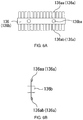
- FIGS. 6A and 6B are diagrams illustrating the construction of an intermediate power supply terminal provided in a light illuminating apparatus according to an embodiment of the present disclosure.
- FIG. 7 is an equivalent circuit diagram of a LED substrate module provided in a light illuminating apparatus according to an embodiment of the present disclosure.
- FIG. 8 is a diagram showing a first variation of a LED unit provided in a light illuminating apparatus according to an embodiment of the present disclosure.
- FIG. 9 is an equivalent circuit diagram of a LED substrate module shown in FIG. 8 .
- FIG. 10 is a diagram showing a second variation of a LED unit provided in a light illuminating apparatus according to an embodiment of the present disclosure.
- FIG. 11 is a diagram showing a third variation of a LED unit provided in a light illuminating apparatus according to an embodiment of the present disclosure.
- FIG. 12 is a diagram showing a fourth variation of a LED unit provided in a light illuminating apparatus according to an embodiment of the present disclosure.
- FIG. 13 is a diagram showing a fourth variation of a LED unit provided in a light illuminating apparatus according to an embodiment of the present disclosure.
- FIG. 14 is a diagram showing a fifth variation of a LED unit provided in a light illuminating apparatus according to an embodiment of the present disclosure.
- FIG. 15 is a diagram showing a sixth variation of a LED unit provided in a light illuminating apparatus according to an embodiment of the present disclosure.
- FIG. 16 is a diagram showing a seventh variation of a LED unit provided in a light illuminating apparatus according to an embodiment of the present disclosure.
- FIG. 17 is a diagram showing a seventh variation of a LED unit provided in a light illuminating apparatus according to an embodiment of the present disclosure.
- FIG. 18 is a diagram showing an eighth variation of a LED unit provided in a light illuminating apparatus according to an embodiment of the present disclosure.
- FIG. 19 is a diagram showing a ninth variation of a LED unit provided in a light illuminating apparatus according to an embodiment of the present disclosure.
- FIG. 1 is a diagram of outward appearance schematically illustrating the construction of a light illuminating apparatus 10 according to an embodiment of the present disclosure.
- the light illuminating apparatus 10 of this embodiment is an apparatus that is mounted in a light source apparatus for curing an ultraviolet (UV) curable ink used as an ink for sheet-fed offset printing or a UV curable resin used as an adhesive in Flat Panel Display (FPD), and is placed facing an object to be illuminated to emit UV light of a line shape to the object to be illuminated.
- UV ultraviolet
- FPD Flat Panel Display
- a lengthwise (line length) direction of UV light of a line shape emitted from the light illuminating apparatus 10 is defined as X-axis direction (first direction), a widthwise (line width) direction is defined as Y-axis direction (second direction), and a direction perpendicular (i.e., orthogonal) to X axis and Y axis is defined as Z-axis direction.
- FIG. 1A is a front view (a diagram when viewed in Z-axis direction) of the light illuminating apparatus 10 of this embodiment
- FIG. 1B is a bottom view (a diagram when viewed in Y-axis direction)
- FIG. 1C is a right side view (a diagram when viewed in X-axis direction).
- the light illuminating apparatus 10 of this embodiment has a plurality of light emitting diode (LED) units 100 in a case not shown.
- FIG. 2 is a diagram of outward appearance schematically illustrating the construction of the LED unit 100
- FIG. 2A is a front view (a diagram when viewed in Z-axis direction) of the LED unit 100
- FIG. 2B is a right side view (a diagram when viewed in X-axis direction) of the LED unit 100 .
- the LED unit 100 includes a base plate 110 , LED substrate modules 120 a , 120 b , 120 c , 120 d , 120 e (hereinafter, collectively referred to as a ⁇ LED substrate module 120 ⁇ ), end power supply terminals 132 , 134 , and an intermediate power supply terminal 136 (hereinafter, the end power supply terminal 132 , 134 and the intermediate power supply terminal 136 are collectively referred to as a ⁇ power supply member 130 ⁇ ), and is an apparatus that emits UV light (as described in detail below).
- 4 LED units 100 are arranged in a line in X-axis direction ( FIG. 1 ).
- the base plate 110 is a rectangular plate-shaped member of metal (for example, aluminum or copper) to fix each component. As shown in FIG. 2 , the base plate 110 of this embodiment has mounting surfaces 114 a , 114 b , 114 c , 114 d , 114 e of an approximately rectangular shape on which five LED substrate modules 120 a , 120 b , 120 c , 120 d , 120 e are mounted respectively.
- Four cylindrical bosses 116 for determining the position of each LED substrate module 120 a , 120 b , 120 c , 120 d , 120 e are formed at the four corners of each mounting surface 114 a , 114 b , 114 c , 114 d , 114 e .
- the base plate 110 of this embodiment has a function of a heat sink that radiates heat from each LED substrate module 120 a , 120 b , 120 c , 120 d , 120 e ) in air.
- a plurality of screw holes (not shown), to which the power supply member 130 (the end power supply terminal 132 , 134 and the intermediate power supply terminal 136 ) as described below is attached, is each formed between each LED substrate module 120 a , 120 b , 120 c , 120 d , 120 e , at the outer part of the LED substrate module 120 a (Y-axis direction upstream side), and at the outer part of the LED substrate module 120 e (Y-axis direction downstream side).
- the LED unit 100 of this embodiment has five LED substrate modules 120 a , 120 b , 120 c , 120 d , 120 e , and the LED substrate modules 120 a , 120 b , 120 c , 120 d , 120 e are respectively attached to the mounting surfaces 114 a , 114 b , 114 c , 114 d , 114 e of the base plate 110 , and because each LED substrate module 120 a , 120 b , 120 c , 120 d , 120 e has the same construction, hereinafter, the construction of the LED substrate module 120 c is representatively described.
- FIG. 3 is a plane view illustrating the construction of the LED substrate module 120 c .
- the LED substrate module 120 c of this embodiment includes a substrate 121 of a rectangular shape parallel to X-axis direction and Y-axis direction, and a plurality of LED devices 125 placed on the substrate 121 .
- the substrate 121 is a rectangular shaped wiring substrate formed of a material having high thermal conductivity (for example, aluminum nitride), and as shown in FIG. 3 , the substrate 121 has 20 LED devices 125 mounted at the rough center of Y-axis direction on the surface at a predetermined interval along X-axis direction by Chip On Board (COB) technology.
- COB Chip On Board
- two anode patterns 122 a , 123 a and two cathode patterns 122 b , 123 b are formed on the substrate 121 to supply power to each LED device 125 , and the anode pattern 122 a and the cathode pattern 122 b and 10 LED devices 125 connected to them form a first circuit, and the anode pattern 123 a and the cathode pattern 123 b and 10 LED devices 125 connected to them form a second circuit. Furthermore, as shown in FIG.
- the anode pattern 122 a in the first circuit, is placed at an upper side (Y-axis direction upstream side) than the cathode pattern 122 b in the drawing, and in the second circuit, the anode pattern 123 a is placed at a lower side (Y-axis direction downstream side) than the cathode pattern 123 b in the drawing, so that a direction in which an electric current flows in the first circuit and a direction in which an electric current flows in the second circuit are opposite to each other.
- the LED device 125 of this embodiment is a so-called vertical LED chip with electrodes arranged in vertical structure, and the LED device 125 is a semiconductor device that emits UV light of 385 nm wavelength when a drive current is supplied through the anode pattern 122 a and the cathode pattern 122 b (or the anode pattern 123 a and the cathode pattern 123 b ).
- An anode electrode is formed on the bottom surface of the LED device 125
- a cathode electrode is formed on the top surface of the LED device 125 .
- the bottom surface (i.e., the anode electrode) of 10 LED devices 125 of the first circuit is directly mounted on the anode pattern 122 a , and the cathode electrodes of 10 LED devices 125 of the first circuit are wire-bonded to the cathode pattern 122 b .
- the bottom surface (i.e., the anode electrode) of 10 LED devices 125 of the second circuit is directly mounted on the anode pattern 123 a , and the cathode electrodes of 10 LED devices 125 of the second circuit are wire-bonded to the cathode pattern 123 b .
- 10 LED devices 125 of the first circuit are connected in parallel and 10 LED devices 125 of the second circuit are connected in parallel, and the first circuit and the second circuit are each independent from each other.
- two anode patterns 122 a , 123 a and two cathode patterns 122 b , 123 b of this embodiment have, respectively, rectangular shaped terminal areas 122 ap , 123 ap , 122 bp , 123 bp (dotted line portions in FIG. 3 ) that come into contact with the end power supply terminal 132 , 134 and the intermediate power supply terminal 136 shown in FIG. 2 .
- the terminal area 122 ap of the anode pattern 122 a and the terminal area 122 bp of the cathode pattern 122 b are placed facing each other in Y-axis direction.
- the terminal area 123 ap of the anode pattern 123 a and the terminal area 123 bp of the cathode pattern 123 b are placed facing each other in Y-axis direction. Furthermore, the terminal area 122 ap of the anode pattern 122 a and the terminal area 123 bp of the cathode pattern 123 b are arranged in a row in X-axis direction, the terminal area 122 bp of the cathode pattern 122 b and the terminal area 123 ap of the anode pattern 123 a are arranged in a row in X-axis direction, and the terminal areas 122 ap , 123 ap of the two anode patterns 122 a , 123 a and the terminal areas 122 bp , 123 bp of the two cathode patterns 122 b , 123 b are respectively point-symmetrical with respect to the center O of the substrate 121 as a symmetry point.
- each electrode i.e., the terminal areas 122 ap , 123 ap , 122 bp , 123 bp ) of the substrate 121 of this embodiment has no directionality with respect to the power supply member 130 . Accordingly, there is no need to pay attention to directionality of the LED substrate module 120 c at all when attaching the LED substrate module 120 c to the base plate 110 as well as replacing the LED substrate module 120 c . Furthermore, the same is the case when attaching the LED substrate modules 120 a , 120 b , 120 d , 120 e to the base plate 110 or replacing the LED substrate modules 120 a , 120 b , 120 d , 120 e . Accordingly, by this construction, maintenance of the light illuminating apparatus 10 ( FIG. 1 ) is remarkably improved.
- through-holes 121 a , 121 b , 121 c , 121 d are formed at the four corners of the substrate 121 , and when each LED substrate module 120 is attached to the base plate 110 , the cylindrical bosses 116 of the base plate 110 are inserted into and pass through the through-holes 121 a , 121 b , 121 c , 121 d to determine the position ( FIG. 2 ). Furthermore, to increase thermal conductivity between the LED substrate modules 120 a , 120 b , 120 c , 120 d , 120 e and the base plate 110 shown in FIG.
- heat-radiating grease or an adhesive having high thermal conductivity may be applied between the back surface of the LED substrate module 120 and each mounting surface 114 a , 114 b , 114 c , 114 d , 114 e.
- the power supply member 130 is attached to the base plate 110 on the LED substrate modules 120 a , 120 b , 120 c , 120 d , 120 e ) (Z-axis direction downstream side), and elastic compression is applied to each substrate 121 of the LED substrate modules 120 a , 120 b , 120 c , 120 d , 120 e against the base plate 110 , and along with this, power is supplied to each electrode (i.e., the terminal areas 122 ap , 123 ap , 122 bp , 123 bp ) of each substrate 121 .
- the power supply member 130 of this embodiment includes a pair of end power supply terminals 132 , 134 disposed at the two end parts of Y-axis direction (i.e., connected to the LED substrate modules 120 a and 120 e ), and eight intermediate power supply terminals 136 placed between each LED substrate module 120 a , 120 b , 120 c , 120 d , 120 e.
- FIG. 4 is a diagram illustrating the construction of the end power supply terminal 132
- FIG. 4A is a plane view
- FIG. 4B is a right side view
- FIG. 5 is a diagram illustrating the construction of the end power supply terminal 134
- FIG. 5A is a plane view
- FIG. 5B is a right side view
- FIG. 6 is a diagram illustrating the construction of the intermediate power supply terminal 136
- FIG. 6A is a plane view
- FIG. 6B is a right side view.
- the end power supply terminal 132 includes a conducting part 132 a formed by punching a thin plate of metal (for example, copper), and a fixing part 132 b of an insulating property (for example, made of resin), each fixing part being fixed to the base plate 110 ( FIG. 2 ) with the conducting part 132 a interposed between in plate thickness direction.
- the end power supply terminal 132 has a plurality of through-holes 132 ba passing through the fixing part 132 b and the conducting part 132 a , and screws not shown are rotatably put into the screw holes (not shown) of the base plate 110 ( FIG. 2 ) through the through-holes 132 ba , to fix the end power supply terminal 132 to the base plate 110 ( FIG. 2 ).
- the conducting part 132 a includes an anode plate 132 aa of an approximately rectangular shape protruding from the fixing part 132 b in Y-axis direction when viewed from the top (when viewed in Z-axis direction), and a contact point part 132 ab protruding in a comb-teeth shape in the direction opposite to the anode plate 132 aa and having a spring property at the front end part. Furthermore, the anode plate 132 aa has a through-hole 132 c.
- the end power supply terminal 134 includes a conducting part 134 a formed by punching a thin plate of metal (for example, copper) and a fixing part 134 b of an insulating property (for example, made of resin), each fixing part being fixed to the base plate 110 with the conducting part 134 a interposed between in plate thickness direction.
- the end power supply terminal 134 has a plurality of through-holes 134 ba passing through the fixing part 134 b and the conducting part 134 a , and screws not shown are rotatably put into the screw holes (not shown) of the base plate 110 ( FIG. 2 ) through the through-holes 134 ba , to fix the end power supply terminal 134 to the base plate 110 ( FIG. 2 ).
- the conducting part 134 a includes a cathode plate 134 aa of an approximately rectangular shape protruding from the fixing part 134 b in Y-axis direction when viewed from the top (when viewed in Z-axis direction), and a contact point part 134 ab protruding in a comb-teeth shape in the direction opposite to the cathode plate 134 aa and having a spring property at the front end part. Furthermore, the cathode plate 134 aa has a through-hole 134 c.
- the anode plate 132 aa and the cathode plate 134 aa of the end power supply terminals 132 , 134 respectively connected to the LED substrate modules 120 a and 120 e are disposed on an anode terminal and a cathode terminal not shown when the end power supply terminals 132 , 134 are attached to the base plate 110 , and when screws not shown are each attached to the anode terminal and the cathode terminal not shown through the through-holes 132 c , 134 c , the anode plate 132 aa and the anode terminal are electrically connected and the cathode plate 134 aa and the cathode terminal are electrically connected.
- the anode terminal and the cathode terminal are connected to a power source apparatus not shown, and when power is supplied from the power source apparatus, power is supplied to the anode plate 132 aa and the cathode plate 134 aa of the LED substrate modules 120 a and 120 e . Furthermore, when the end power supply terminal 132 connected to the LED substrate modules 120 a and 120 e is attached to the base plate 110 , the contact point part 132 ab presses the terminal areas 122 ap and 123 ap of the LED substrate modules 120 a and 120 e to electrically and thermally connect the substrate 121 ( FIG. 3 ) of the LED substrate modules 120 a and 120 e to the base plate 110 .
- the contact point part 134 presses the terminal areas 123 bp and 122 bp of the LED substrate modules 120 a and 120 e to electrically and thermally connect the substrate 121 ( FIG. 3 ) of the LED substrate modules 120 a and 120 e to the base plate 110 .
- the intermediate power supply terminal 136 is a member which is each placed between each LED substrate module 120 a , 120 b , 120 c , 120 d , 120 e to respectively connect in series the first circuit and the second circuit of each LED substrate module 120 a , 120 b , 120 c , 120 d , 120 e ( FIG. 3 ).
- the intermediate power supply terminal 136 includes a conducting part 136 a formed by punching a thin plate of metal (for example, copper) and a fixing part 136 b of an insulating property (for example, made of resin), each fixing part being fixed to the base plate 110 ( FIG. 2 ) with the conducting part 136 a interposed between in plate thickness direction.
- the intermediate power supply terminal 136 has a plurality of through-holes 136 ba passing through the fixing part 136 b and the conducting part 136 a , and screws not shown are rotatably put into the screw holes (not shown) of the base plate 110 ( FIG. 2 ) through the through-holes 136 ba , to fix the intermediate power supply terminal 136 to the base plate 110 ( FIG. 2 ).
- the conducting part 136 a has contact point parts 136 aa , 136 ab that protrude from the fixing part 136 b in a comb-teeth shape in Y-axis direction and in the direction opposite to Y-axis direction, and have a spring property at the front end part. Furthermore, as shown in FIG. 6 , the conducting part 136 a has contact point parts 136 aa , 136 ab that protrude from the fixing part 136 b in a comb-teeth shape in Y-axis direction and in the direction opposite to Y-axis direction, and have a spring property at the front end part. Furthermore, as shown in FIG.
- each first circuit of each LED substrate module 120 a , 120 b , 120 c , 120 d , 120 e is connected in series and each second circuit is connected in series, and an equivalent circuit diagram is as shown in FIG. 7 .
- each first circuit i.e., 10 LED devices 125 connected in parallel
- each second circuit i.e., 10 LED devices 125 connected in parallel
- the LED substrate modules 120 a , 120 b , 120 c , 120 d , 120 e is each expressed as one LED symbol.
- the power supply member 130 connecting five LED substrate modules 120 a , 120 b , 120 c , 120 d , 120 e in series has a function to electrically connect each substrate 121 and a function to fix to the base plate 110 ( FIG. 2 ). Accordingly, attachment and replacement of the LED substrate modules 120 a , 120 b , 120 c , 120 d , 120 e can be easily accomplished by attachment and removal of the power supply member 130 .
- each LED substrate module 120 a , 120 b , 120 c , 120 d , 120 e has no directionality with respect to the power supply member 130 , there is no need to pay attention to the directionality at all when attaching each LED substrate module 120 a , 120 b , 120 c , 120 d , 120 e to the base plate 110 and even when replacing each LED substrate module 120 a , 120 b , 120 c , 120 d , 120 e . Accordingly, by this construction, maintenance of the light illuminating apparatus 10 is remarkably improved.
- the light illuminating apparatus 10 of this embodiment has a plurality of LED units 100
- the present disclosure is not necessarily limited thereto, and the light illuminating apparatus 10 may have one LED unit 100 according to use.
- this embodiment is configured to emit UV light of 385 nm wavelength
- the present disclosure is not limited thereto, and may be configured to emit UV light of other wavelength (for example, 365 nm wavelength, 385 nm wavelength, 395 nm wavelength, 405 nm wavelength) or to emit visible light or infrared light.
- five LED substrate modules 120 a , 120 b , 120 c , 120 d , 120 e have the same LED device 125 mounted thereon, for example, each LED substrate module 120 a , 120 b , 120 c , 120 d , 120 e may have LED devices of different wavelengths mounted thereon to irradiate light of mixed wavelengths.
- the LED substrate module 120 of this embodiment has a first circuit and a second circuit independent from each other in Y-axis direction ( FIG. 3 ), the present disclosure is not necessarily limited thereto.
- the terminal area 122 ap , 123 ap of the anode pattern 122 a , 123 a and the terminal area 122 bp , 123 bp of the cathode pattern 122 b , 123 b on the substrate 121 may be point-symmetrical with the respect of the center O of the substrate 121 as a symmetry point, and 2n circuits (n is an integer greater than or equal to 1) independent from each other in the first direction may be formed on the substrate 121 .
- the present disclosure is not limited thereto, and M LED substrate modules 120 (M is an integer greater than or equal to 2) may be placed in Y-axis direction. Accordingly, provided that the number of circuits of each LED substrate module 120 and the number of LED substrate modules 120 is generalized and a relationship between the LED substrate module 120 and the power supply member 130 is considered, the light illuminating apparatus of the present disclosure is as below.
- the intermediate power supply terminal 136 (connecting member) is placed between the terminal area 122 bp or 123 bp (second electrode) and the terminal area 122 ap or 123 ap (first electrode) facing each other between the i th LED substrate module 120 (i is an integer greater than or equal to 1 and less than or equal to M ⁇ 1) and the i+1 th LED substrate module 120 .
- the end power supply terminal 132 (first power supply member) is connected to the terminal area 122 ap or 123 ap (first electrode) of the 2j ⁇ 1 th circuit (j is an integer greater than or equal to 1 and less than or equal to n) formed in the 1 st LED substrate module 120 and the 2j th circuit formed in the M th LED substrate module 120 .
- the end power supply terminal 134 (second power supply member) is connected to the terminal area 122 bp or 123 bp (second electrode) of the 2j ⁇ 1 th circuit formed in the M th LED substrate module 120 and the 2j th circuit formed in the 1 st LED substrate module 120 .
- FIG. 8 is a diagram showing a first variation of the LED unit 100 of this embodiment.
- a LED unit 100 A of this variation is different from the LED unit 100 of this embodiment in the respect that the LED unit 100 A has a short bar 138 between the end power supply terminals 132 , 134 connected to the LED substrate module 120 a .
- FIG. 9 is an equivalent circuit diagram of the LED unit 100 A of this variation. As shown in FIG. 9 , in this variation, because the end power supply terminals 132 , 134 are connected by the short bar 138 , the first circuit and the second circuit are successive, forming a series circuit.
- the LED substrate module 120 a does not need to have an anode terminal for connecting to the anode plate 132 aa , and a cathode terminal for connecting to the cathode plate 134 aa.
- FIG. 10 is a diagram showing a second variation of the LED unit 100 of this embodiment.
- a LED unit 100 B of this variation is different from the LED unit 100 A of the first variation in the respect that the LED unit 100 B has an integrated end power supply terminal 139 instead of the end power supply terminal 132 , 134 connected to the LED substrate module 120 a and the short bar 138 .
- the light illuminating apparatus of the present disclosure is as below. That is, in the light illuminating apparatus, when 1 st to M th LED substrate modules 120 are set in a sequential order along Y-axis direction and 1 st to 2n th circuits are set in a sequential order along X-axis direction in each LED substrate module 120 , the intermediate power supply terminal 136 (first connecting member) is placed between the terminal area 122 bp or 123 bp (second electrode) and the terminal area 122 ap or 123 ap (first electrode) facing each other between the i th LED substrate module 120 (i is an integer greater than or equal to 1 and less than or equal to M ⁇ 1) and the i+1 th LED substrate module 120 .
- the end power supply terminal 139 (second connecting member) is placed between the terminal area 122 bp or 123 bp (second electrode) of the 2j ⁇ 1 th circuit (j is an integer greater than or equal to 1 and less than or equal to n) and the terminal area 122 ap or 123 ap (first electrode) of the 2j th circuit formed in the M th LED substrate module 120 .
- the end power supply terminal 132 (first power supply member) is connected to the terminal area 122 ap or 123 ap (first electrode) of the 2j ⁇ 1 th circuit formed in the 1 st LED substrate module 120 .
- the end power supply terminal 134 (second power supply member) is connected to the terminal area 122 bp or 123 bp (second electrode) of the 2j th circuit formed in the 1 st LED substrate module 120 .
- FIG. 11 is a diagram showing a third variation of the LED unit 100 of this embodiment.
- a LED unit 100 C this variation is different from the LED unit 100 of this embodiment in the respect that the LED unit 100 C is configured such that the LED substrate modules 120 a , 120 b , 120 c are arranged in X-axis direction, the first circuit and the second circuit of each LED substrate module 120 a , 120 b , 120 c are connected by the end power supply terminal 139 , and the second circuit of each LED substrate module 120 a , 120 b , 120 c and the first circuit of an adjacent LED substrate module are also connected by the end power supply terminal 139 .
- the end power supply terminal 139 is installed between the terminal area 122 bp and the terminal area 123 ap of each LED substrate module 120 a , 120 b , 120 c , between the terminal area 123 bp of the LED substrate module 120 a and the terminal area 122 ap of the LED substrate module 120 b , and between the terminal area 123 bp of the LED substrate module 120 b and the terminal area 122 ap of the LED substrate module 120 c .
- the dimension in Y-axis direction can be restrained.
- the light illuminating apparatus of the present disclosure is as below. That is, in the light illuminating apparatus, when 1 st to N th LED substrate modules 120 are set in a sequential order along X-axis direction and 1 st to 2n th circuits are set in a sequential order along X-axis direction in each LED substrate module 120 , the end power supply terminal 139 (connecting member) is placed between the terminal area 122 bp or 123 bp (second electrode) of the j th circuit (j is an integer greater than or equal to 1 and less than or equal to 2n ⁇ 1) and the terminal area 122 ap or 123 ap (first electrode) of the j+1 th circuit formed in the i th LED substrate module 120 (i is an integer greater than or equal to 1 and less than or equal to N ⁇ 1)
- the end power supply terminal 132 (first power supply member) is connected to the terminal area 122 ap or 123 ap (first electrode) of the 1 st circuit formed in the 1 st LED substrate module 120 .
- the end power supply terminal 134 (second power supply member) is connected to the terminal area 122 bp or 123 bp (second electrode) of the 2n th circuit formed in the N th LED substrate module 120 .
- FIGS. 12 and 13 are diagrams showing a fourth variation of the LED unit 100 of this embodiment.
- a LED unit 100 D of this variation is different from the LED unit 100 of this embodiment, as shown in FIG. 13 , in the respect of the LED unit 100 D on which a substrate 121 M having a first circuit and a second circuit is mounted, in which four circuits each consisting of ten LED devices 125 connected in parallel are connected in series, forming each of the first circuit and the second circuit.
- the LED unit 100 D of this variation is different from the LED unit 100 A of the first variation in the respect that LED substrate modules 120 Ma and 120 Mb having the substrate 121 M mounted thereon are provided in Y-axis direction.
- the number of intermediate power supply terminals 136 connecting the substrates 121 M can be reduced as compared to the first variation, making it possible to easily realize the LED unit 100 D with large area and high output. Furthermore, it is possible to reduce manufacturing costs as compared to the construction using one large-area substrate.
- FIG. 14 is a diagram showing a fifth variation of the LED unit 100 of this embodiment.
- a LED unit 100 E of this variation is different from the LED unit 100 D of the fourth variation in the respect that the LED unit 100 E has the integrated end power supply terminal 139 instead of the end power supply terminal 132 , 134 connected to the LED substrate module 120 Mb. That is, in this variation, the end power supply terminal 139 is installed between the terminal area 122 bp and the terminal area 123 ap of the LED substrate module 120 Mb.
- the first circuit and the second circuit are successive, forming a series circuit in the LED unit 100 E, in the same way as the first variation and the second variation.
- FIG. 15 is a diagram showing a sixth variation of the LED unit 100 of this embodiment.
- a LED unit 100 F of this variation is different from the LED unit 100 E of the fifth variation in the respect that the LED unit 100 F is configured such that the LED substrate modules 120 Ma, 120 Mb are arranged in X-axis direction, the first circuit and the second circuit of each LED substrate module 120 Ma, 120 Mb are connected by the end power supply terminal 139 , and the second circuit of the LED substrate module 120 Ma and the first circuit of the adjacent LED substrate module 120 Mb are also connected by the end power supply terminal 139 .
- the end power supply terminal 139 is installed between the terminal area 122 bp and the terminal area 123 ap of each LED substrate module 120 Ma, 120 Mb, and between the terminal area 123 bp of the LED substrate module 120 Ma and the terminal area 122 ap of the LED substrate module 120 Mb.
- the dimension in Y-axis direction can be restrained.
- FIGS. 16 and 17 are diagrams showing a seventh variation of the LED unit 100 of this embodiment.
- a LED unit 100 G of this variation is different from the LED unit 100 D of the fourth variation in the respect that the LED unit 100 G has a substrate 121 N shown in FIG. 17 mounted thereon, and an end power supply terminal 132 G, 134 G and an intermediate power supply terminal 136 G instead of the end power supply terminal 132 , 134 and the intermediate power supply terminal 136 .
- the substrate 121 N of this variation is different from the substrate 121 M of the fourth variation ( FIG.
- the substrate 121 N has a through-hole 121 Nx into which a screw (not shown) for fixing the substrate 121 N is inserted, passing therethrough, at the rough center of the substrate 121 N, and through-holes 121 Na, 121 Nb, 121 Nc, 121 Nd for fixing the end power supply terminal 132 G, 134 G or the intermediate power supply terminal 136 G at the terminal areas 122 ap , 122 bp , 123 ap , 123 bp.
- the end power supply terminal 132 G is a thin plate-shaped member of metal (for example, copper) to supply power to LED substrate modules 120 Na, 120 Nb.
- the end power supply terminal 132 G has a through-hole 132 Ga for fixing to the substrate 121 N and a through-hole 132 Gb for fixing to the anode terminal not shown.
- the end power supply terminal 132 G is attached to the terminal area 122 ap of the LED substrate module 120 Na and the terminal area 123 ap of the LED substrate module 120 Nb, and is each fixed by a screw (not shown) passing through the through-hole 132 Ga and the through-hole 121 Na of the LED substrate module 120 Na ( FIG. 17 ) and a screw (not shown) passing through the through-hole 132 Ga and the through-hole 121 Nc of the LED substrate module 120 Nb ( FIG. 17 ).
- each end power supply terminal 132 G is fixed to the anode terminal (not shown) by a screw (not shown) passing through the through-hole 132 Gb.
- the end power supply terminal 134 G is a thin plate-shaped member of metal (for example, copper) to supply power to the LED substrate module 120 Na, 120 Nb.
- the end power supply terminal 134 G has a through-hole 134 Ga for fixing to the substrate 121 N and a through-hole 134 Gb for fixing to the cathode terminal not shown.
- the end power supply terminal 134 G is attached to the terminal area 123 bp of the LED substrate module 120 Na and the terminal area 122 bp of the LED substrate module 120 Nb, and is each fixed by a screw (not shown) passing through the through-hole 134 Ga and the through-hole 121 Nd of the LED substrate module 120 Na ( FIG.
- each end power supply terminal 134 G is fixed to the cathode terminal (not shown) by a screw (not shown) passing through the through-hole 134 Gb.
- the intermediate power supply terminal 136 G is a thin plate-shaped member of metal (for example, copper) respectively connecting the first circuit and the second circuit of the LED substrate module 120 Na, 120 Nb in series.
- the intermediate power supply terminal 136 G has through-holes 136 Ga, 136 Gb for fixing to the substrate 121 N.
- the intermediate power supply terminal 136 G is attached between the terminal area 122 bp of the LED substrate module 120 Na and the terminal area 122 ap of the LED substrate module 120 Nb, and between the terminal area 123 ap of the LED substrate module 120 Na and the terminal area 123 bp of the LED substrate module 120 Nb.
- the intermediate power supply terminal 136 G placed between the terminal area 122 bp of the LED substrate module 120 Na and the terminal area 122 ap of the LED substrate module 120 Nb is fixed by a screw (not shown) passing through the through-hole 136 Ga and the through-hole 121 Nb of the LED substrate module 120 Na ( FIG. 17 ) and a screw (not shown) passing through the through-hole 136 Gb and the through-hole 121 Na of the LED substrate module 120 Nb ( FIG. 17 ).
- the intermediate power supply terminal 136 G placed between the terminal area 123 ap of the LED substrate module 120 Na and the terminal area 123 bp of the LED substrate module 120 Nb is fixed by a screw (not shown) passing through the through-hole 136 Ga and the through-hole 121 Nd of the LED substrate module 120 Nb ( FIG. 17 ) and a screw (not shown) passing through the through-hole 136 Gb and the through-hole 121 Nc of the LED substrate module 120 Na ( FIG. 17 ).
- the end power supply terminal 132 G, 134 G and the intermediate power supply terminal 136 G are directly fixed to the LED substrate module 120 Na, 120 Nb. Furthermore, in this variation, dissimilar to the LED unit 100 D of the fourth variation, because it is impossible to press the LED substrate modules 120 Na and 120 Nb by the end power supply terminal 132 G, 134 G and the intermediate power supply terminal 136 G, a screw not shown is allowed to be inserted into and pass through the through-hole 121 Nx to fix each of the LED substrate modules 120 Na and 120 Nb. By the construction of this variation, it is possible to firmly fix the LED substrate modules 120 Na and 120 Nb by a screw.
- FIG. 18 is a diagram showing an eighth variation of the LED unit 100 of this embodiment.
- a LED unit 100 H of this variation is different from the LED unit 100 G of the seventh variation in the respect that the LED unit 100 H uses the end power supply terminal 135 connecting the terminal area 122 bp and the terminal area 123 ap of the LED substrate module 120 Nb, instead of the end power supply terminal 132 G, 134 G connected to the terminal areas 122 bp and 123 a of the LED substrate module 120 Nb.
- the first circuit and the second circuit are successive, forming a series circuit in the LED unit 100 H, in the same way as the first variation and the second variation.
- FIG. 19 is a diagram showing a ninth variation of the LED unit 100 of this embodiment.
- a LED unit 100 I of this variation is different from the LED unit 100 H of the eighth variation in the respect that the LED substrate modules 120 Na, 120 Nb are arranged in X-axis direction, the first circuit and the second circuit of each LED substrate module 120 Na, 120 Nb are connected by the end power supply terminal 135 , and the second circuit of the LED substrate module 120 Na and the first circuit of the adjacent LED substrate module 120 Nb are also connected by the end power supply terminal 135 .
- the end power supply terminal 135 is installed between the terminal area 122 bp and the terminal area 123 ap of each LED substrate module 120 Na, 120 Nb, and between the terminal area 123 bp of the LED substrate module 120 Na and the terminal area 122 ap of the LED substrate module 120 Nb.
- the dimension in Y-axis direction can be restrained.
Landscapes
- Engineering & Computer Science (AREA)
- Microelectronics & Electronic Packaging (AREA)
- Power Engineering (AREA)
- General Engineering & Computer Science (AREA)
- Computer Hardware Design (AREA)
- Physics & Mathematics (AREA)
- Manufacturing & Machinery (AREA)
- Condensed Matter Physics & Semiconductors (AREA)
- General Physics & Mathematics (AREA)
- Optics & Photonics (AREA)
- Led Device Packages (AREA)
- Fastening Of Light Sources Or Lamp Holders (AREA)
- Non-Portable Lighting Devices Or Systems Thereof (AREA)
- Supply, Installation And Extraction Of Printed Sheets Or Plates (AREA)
Applications Claiming Priority (2)
| Application Number | Priority Date | Filing Date | Title |
|---|---|---|---|
| JP2016-073751 | 2016-03-31 | ||
| JP2016073751A JP6360514B2 (ja) | 2016-03-31 | 2016-03-31 | Led基板及びそれを有する光照射装置 |
Publications (2)
| Publication Number | Publication Date |
|---|---|
| US20170284642A1 US20170284642A1 (en) | 2017-10-05 |
| US10782003B2 true US10782003B2 (en) | 2020-09-22 |
Family
ID=58360933
Family Applications (1)
| Application Number | Title | Priority Date | Filing Date |
|---|---|---|---|
| US15/464,707 Active 2038-07-07 US10782003B2 (en) | 2016-03-31 | 2017-03-21 | LED substrate and light illuminating apparatus with the same |
Country Status (6)
| Country | Link |
|---|---|
| US (1) | US10782003B2 (zh) |
| EP (1) | EP3226295B1 (zh) |
| JP (1) | JP6360514B2 (zh) |
| KR (1) | KR102147464B1 (zh) |
| CN (1) | CN107388050A (zh) |
| TW (1) | TWI723138B (zh) |
Families Citing this family (2)
| Publication number | Priority date | Publication date | Assignee | Title |
|---|---|---|---|---|
| US10054849B2 (en) * | 2016-05-17 | 2018-08-21 | Seiko Epson Corporation | Light source device and projector |
| KR102650608B1 (ko) * | 2020-12-18 | 2024-03-25 | 세메스 주식회사 | 광 처리 부재, 그를 포함하는 기판 처리 장치 및 기판 처리 방법 |
Citations (14)
| Publication number | Priority date | Publication date | Assignee | Title |
|---|---|---|---|---|
| US4845405A (en) * | 1986-05-14 | 1989-07-04 | Sanyo Electric Co., Ltd. | Monolithic LED display |
| JP2006228557A (ja) | 2005-02-17 | 2006-08-31 | Koizumi Sangyo Corp | El光源装置 |
| JP2006295084A (ja) | 2005-04-14 | 2006-10-26 | Citizen Electronics Co Ltd | 発光ダイオードのパッケージ構造 |
| US7259403B2 (en) * | 2001-08-09 | 2007-08-21 | Matsushita Electric Industrial Co., Ltd. | Card-type LED illumination source |
| WO2008091837A2 (en) | 2007-01-22 | 2008-07-31 | Cree Led Lighting Solutions, Inc. | Fault tolerant light emitters, systems incorporating fault tolerant light emitters and methods of fabricating fault tolerant light emitters |
| JP2009147082A (ja) | 2007-12-13 | 2009-07-02 | Rohm Co Ltd | 半導体発光ユニットおよびこれを用いた半導体発光装置 |
| JP2009534792A (ja) | 2006-04-21 | 2009-09-24 | クリー インコーポレイテッド | 全般照明用の固体照明器具 |
| US20090316409A1 (en) * | 2008-06-24 | 2009-12-24 | Yu-Sik Kim | Sub-mount, light emitting device including sub-mount and methods of manufacturing such sub-mount and/or light emitting device |
| CN102374401A (zh) | 2010-08-19 | 2012-03-14 | 富士迈半导体精密工业(上海)有限公司 | 发光二极管灯具 |
| EP2442362A1 (en) | 2010-10-13 | 2012-04-18 | Intematix Technology Center Corp. | Light emitting device |
| WO2013040453A2 (en) | 2011-09-16 | 2013-03-21 | Air Motion Systems, Inc. | Assembly and interconnection method for high-power led devices |
| WO2014207620A1 (en) | 2013-06-28 | 2014-12-31 | Koninklijke Philips N.V. | Bonding led die to lead frame strips |
| JP2015053160A (ja) | 2013-09-06 | 2015-03-19 | 京セラコネクタプロダクツ株式会社 | 照明器具 |
| JP2015153771A (ja) | 2014-02-10 | 2015-08-24 | 京セラ株式会社 | 光照射装置および印刷装置 |
Family Cites Families (10)
| Publication number | Priority date | Publication date | Assignee | Title |
|---|---|---|---|---|
| JP2001307506A (ja) * | 2000-04-17 | 2001-11-02 | Hitachi Ltd | 白色発光装置および照明器具 |
| JP2004266246A (ja) * | 2003-02-12 | 2004-09-24 | Toyoda Gosei Co Ltd | 発光装置 |
| DE602006020486D1 (de) * | 2005-12-16 | 2011-04-14 | Koninkl Philips Electronics Nv | Miteinander verbindbare beleuchtungsmodule umfassendes beleuchtungssystem |
| TWI440210B (zh) * | 2007-01-22 | 2014-06-01 | Cree Inc | 使用發光裝置外部互連陣列之照明裝置及其製造方法 |
| KR100951843B1 (ko) * | 2007-06-28 | 2010-04-12 | (주) 아모엘이디 | 필터 및 반도체 패키지 |
| WO2010050694A2 (ko) * | 2008-10-29 | 2010-05-06 | 서울옵토디바이스주식회사 | 발광 다이오드 |
| JP2011018695A (ja) * | 2009-07-07 | 2011-01-27 | Stanley Electric Co Ltd | 発光装置およびその製造方法 |
| JP2013115351A (ja) * | 2011-11-30 | 2013-06-10 | Sumitomo Metal Mining Co Ltd | Led波長変換部材とその製造方法 |
| KR101434835B1 (ko) * | 2012-10-29 | 2014-09-02 | 연세대학교 산학협력단 | 발광 효율을 개선할 수 있는 구조를 갖는 led 패키지 및 그 제조방법 |
| KR102291493B1 (ko) * | 2016-08-11 | 2021-08-20 | 삼성디스플레이 주식회사 | 컬러 필터 및 이를 포함하는 표시 장치 |
-
2016
- 2016-03-31 JP JP2016073751A patent/JP6360514B2/ja active Active
-
2017
- 2017-03-07 TW TW106107446A patent/TWI723138B/zh not_active IP Right Cessation
- 2017-03-16 KR KR1020170033063A patent/KR102147464B1/ko active IP Right Grant
- 2017-03-20 EP EP17161735.0A patent/EP3226295B1/en active Active
- 2017-03-21 US US15/464,707 patent/US10782003B2/en active Active
- 2017-03-22 CN CN201710171840.8A patent/CN107388050A/zh active Pending
Patent Citations (20)
| Publication number | Priority date | Publication date | Assignee | Title |
|---|---|---|---|---|
| US4845405A (en) * | 1986-05-14 | 1989-07-04 | Sanyo Electric Co., Ltd. | Monolithic LED display |
| US7259403B2 (en) * | 2001-08-09 | 2007-08-21 | Matsushita Electric Industrial Co., Ltd. | Card-type LED illumination source |
| JP2006228557A (ja) | 2005-02-17 | 2006-08-31 | Koizumi Sangyo Corp | El光源装置 |
| JP2006295084A (ja) | 2005-04-14 | 2006-10-26 | Citizen Electronics Co Ltd | 発光ダイオードのパッケージ構造 |
| JP2009534792A (ja) | 2006-04-21 | 2009-09-24 | クリー インコーポレイテッド | 全般照明用の固体照明器具 |
| WO2008091837A2 (en) | 2007-01-22 | 2008-07-31 | Cree Led Lighting Solutions, Inc. | Fault tolerant light emitters, systems incorporating fault tolerant light emitters and methods of fabricating fault tolerant light emitters |
| US20080179602A1 (en) | 2007-01-22 | 2008-07-31 | Led Lighting Fixtures, Inc. | Fault tolerant light emitters, systems incorporating fault tolerant light emitters and methods of fabricating fault tolerant light emitters |
| JP2009147082A (ja) | 2007-12-13 | 2009-07-02 | Rohm Co Ltd | 半導体発光ユニットおよびこれを用いた半導体発光装置 |
| US20090316409A1 (en) * | 2008-06-24 | 2009-12-24 | Yu-Sik Kim | Sub-mount, light emitting device including sub-mount and methods of manufacturing such sub-mount and/or light emitting device |
| CN102374401A (zh) | 2010-08-19 | 2012-03-14 | 富士迈半导体精密工业(上海)有限公司 | 发光二极管灯具 |
| EP2442362A1 (en) | 2010-10-13 | 2012-04-18 | Intematix Technology Center Corp. | Light emitting device |
| US20120091476A1 (en) * | 2010-10-13 | 2012-04-19 | Intematix Technology Center Corporation | Light emitting device |
| WO2013040453A2 (en) | 2011-09-16 | 2013-03-21 | Air Motion Systems, Inc. | Assembly and interconnection method for high-power led devices |
| US20130087722A1 (en) | 2011-09-16 | 2013-04-11 | Michael H. Brown | Assembly and interconnection method for high-power led devices |
| JP2014528171A (ja) | 2011-09-16 | 2014-10-23 | エアー・モーション・システムズ・インコーポレイテッドAir Motion Systems, Inc. | 高出力led装置の組立及び相互接続の方法 |
| WO2014207620A1 (en) | 2013-06-28 | 2014-12-31 | Koninklijke Philips N.V. | Bonding led die to lead frame strips |
| US20160329473A1 (en) | 2013-06-28 | 2016-11-10 | Koninklijke Philips N.V. | Bonding LED Die to Lead Frame Strips |
| US20170092628A1 (en) | 2013-06-28 | 2017-03-30 | Koninklijke Philips N.V. | Bonding led die to lead frame strips |
| JP2015053160A (ja) | 2013-09-06 | 2015-03-19 | 京セラコネクタプロダクツ株式会社 | 照明器具 |
| JP2015153771A (ja) | 2014-02-10 | 2015-08-24 | 京セラ株式会社 | 光照射装置および印刷装置 |
Also Published As
| Publication number | Publication date |
|---|---|
| EP3226295A1 (en) | 2017-10-04 |
| CN107388050A (zh) | 2017-11-24 |
| JP6360514B2 (ja) | 2018-07-18 |
| KR102147464B1 (ko) | 2020-08-25 |
| EP3226295B1 (en) | 2020-07-15 |
| TW201736007A (zh) | 2017-10-16 |
| KR20170113128A (ko) | 2017-10-12 |
| JP2017188489A (ja) | 2017-10-12 |
| US20170284642A1 (en) | 2017-10-05 |
| TWI723138B (zh) | 2021-04-01 |
Similar Documents
| Publication | Publication Date | Title |
|---|---|---|
| US20120020089A1 (en) | Light emitting diode light bar | |
| TW201030277A (en) | Separation-type LED lamp tube | |
| KR20150113860A (ko) | 광 조사 장치 | |
| US9304353B2 (en) | Direct backlight module | |
| US10782003B2 (en) | LED substrate and light illuminating apparatus with the same | |
| US10362642B2 (en) | Light emitting device and light illuminating apparatus comprising the light emitting device | |
| US10784425B2 (en) | Light illuminating module and wire board for LED device | |
| JP2011018695A (ja) | 発光装置およびその製造方法 | |
| CN111511154B (zh) | 电路基板固定构造以及具备该构造的光照射装置 | |
| JP2012119624A (ja) | 発光モジュールおよび発光装置 | |
| KR101918548B1 (ko) | 광 조사 장치 | |
| KR101349294B1 (ko) | 발광다이오드 모듈 및 조명기구 | |
| KR102458620B1 (ko) | Led 조명 디바이스 | |
| CN102200235A (zh) | Led发光条 | |
| KR101191566B1 (ko) | 엘이디 조명기기 | |
| WO2023182191A1 (ja) | 光照射モジュール、光照射装置 | |
| KR20110049518A (ko) | 조명용 led 모듈 | |
| KR100826451B1 (ko) | 분리형 기판 및 이를 이용한 발광장치 | |
| KR20230001067U (ko) | 5mm 단위 길이 측정 및 5mm 미세 길이 절단이 가능한 LED 바 PCB 제작 방법 | |
| TWI420959B (zh) | 發光二極體模組 | |
| JP3157746U (ja) | 並列led発光素子の並列発光回路 | |
| TWI381125B (zh) | 照明裝置 | |
| KR20100121416A (ko) | 광원 | |
| KR20140095989A (ko) | 패키지공정 및 회로기판이 없는 발광 다이오드장치 및 그의 제조방법 | |
| JP2017120686A (ja) | 発光モジュール、ランプ装置および照明装置 |
Legal Events
| Date | Code | Title | Description |
|---|---|---|---|
| AS | Assignment |
Owner name: HOYA CANDEO OPTRONICS CORPORATION, JAPAN Free format text: ASSIGNMENT OF ASSIGNORS INTEREST;ASSIGNOR:WATANABE, HIROAKI;REEL/FRAME:041660/0577 Effective date: 20170301 |
|
| STPP | Information on status: patent application and granting procedure in general |
Free format text: DOCKETED NEW CASE - READY FOR EXAMINATION |
|
| STPP | Information on status: patent application and granting procedure in general |
Free format text: NON FINAL ACTION MAILED |
|
| STPP | Information on status: patent application and granting procedure in general |
Free format text: RESPONSE TO NON-FINAL OFFICE ACTION ENTERED AND FORWARDED TO EXAMINER |
|
| STPP | Information on status: patent application and granting procedure in general |
Free format text: EX PARTE QUAYLE ACTION MAILED |
|
| STPP | Information on status: patent application and granting procedure in general |
Free format text: RESPONSE TO EX PARTE QUAYLE ACTION ENTERED AND FORWARDED TO EXAMINER |
|
| STPP | Information on status: patent application and granting procedure in general |
Free format text: PUBLICATIONS -- ISSUE FEE PAYMENT VERIFIED |
|
| STCF | Information on status: patent grant |
Free format text: PATENTED CASE |
|
| FEPP | Fee payment procedure |
Free format text: MAINTENANCE FEE REMINDER MAILED (ORIGINAL EVENT CODE: REM.); ENTITY STATUS OF PATENT OWNER: LARGE ENTITY |