US10386956B2 - Organic light-emitting display panel and organic light-emitting display device having built-in touchscreen - Google Patents
Organic light-emitting display panel and organic light-emitting display device having built-in touchscreen Download PDFInfo
- Publication number
- US10386956B2 US10386956B2 US15/391,625 US201615391625A US10386956B2 US 10386956 B2 US10386956 B2 US 10386956B2 US 201615391625 A US201615391625 A US 201615391625A US 10386956 B2 US10386956 B2 US 10386956B2
- Authority
- US
- United States
- Prior art keywords
- touch
- organic light
- emitting display
- electrode
- display panel
- Prior art date
- Legal status (The legal status is an assumption and is not a legal conclusion. Google has not performed a legal analysis and makes no representation as to the accuracy of the status listed.)
- Active
Links
- 238000005538 encapsulation Methods 0.000 claims abstract description 87
- 239000002184 metal Substances 0.000 claims description 79
- 229910052751 metal Inorganic materials 0.000 claims description 79
- 238000009413 insulation Methods 0.000 claims description 24
- 239000003990 capacitor Substances 0.000 claims description 10
- 239000011159 matrix material Substances 0.000 claims 2
- 239000010410 layer Substances 0.000 description 225
- 150000002739 metals Chemical class 0.000 description 31
- 230000003071 parasitic effect Effects 0.000 description 15
- 238000000034 method Methods 0.000 description 9
- 238000012545 processing Methods 0.000 description 9
- 238000004519 manufacturing process Methods 0.000 description 6
- 230000008859 change Effects 0.000 description 5
- 238000010586 diagram Methods 0.000 description 4
- 230000035945 sensitivity Effects 0.000 description 4
- 239000004642 Polyimide Substances 0.000 description 3
- 239000011368 organic material Substances 0.000 description 3
- 229920001721 polyimide Polymers 0.000 description 3
- 229910003460 diamond Inorganic materials 0.000 description 2
- 239000010432 diamond Substances 0.000 description 2
- 239000011229 interlayer Substances 0.000 description 2
- 230000002093 peripheral effect Effects 0.000 description 2
- 239000011241 protective layer Substances 0.000 description 2
- 230000004044 response Effects 0.000 description 2
- 230000002123 temporal effect Effects 0.000 description 2
- QVGXLLKOCUKJST-UHFFFAOYSA-N atomic oxygen Chemical compound [O] QVGXLLKOCUKJST-UHFFFAOYSA-N 0.000 description 1
- 239000003086 colorant Substances 0.000 description 1
- 230000003247 decreasing effect Effects 0.000 description 1
- 238000013461 design Methods 0.000 description 1
- 238000011161 development Methods 0.000 description 1
- 230000000694 effects Effects 0.000 description 1
- 230000005674 electromagnetic induction Effects 0.000 description 1
- 239000012535 impurity Substances 0.000 description 1
- 238000001764 infiltration Methods 0.000 description 1
- 230000008595 infiltration Effects 0.000 description 1
- 230000002452 interceptive effect Effects 0.000 description 1
- 239000004973 liquid crystal related substance Substances 0.000 description 1
- 239000007769 metal material Substances 0.000 description 1
- 238000012986 modification Methods 0.000 description 1
- 230000004048 modification Effects 0.000 description 1
- 239000012044 organic layer Substances 0.000 description 1
- 229910052760 oxygen Inorganic materials 0.000 description 1
- 239000001301 oxygen Substances 0.000 description 1
- 238000000059 patterning Methods 0.000 description 1
- 230000008054 signal transmission Effects 0.000 description 1
- 239000002356 single layer Substances 0.000 description 1
- 239000000126 substance Substances 0.000 description 1
- 239000000758 substrate Substances 0.000 description 1
Images


Classifications
-
- H—ELECTRICITY
- H10—SEMICONDUCTOR DEVICES; ELECTRIC SOLID-STATE DEVICES NOT OTHERWISE PROVIDED FOR
- H10K—ORGANIC ELECTRIC SOLID-STATE DEVICES
- H10K59/00—Integrated devices, or assemblies of multiple devices, comprising at least one organic light-emitting element covered by group H10K50/00
- H10K59/40—OLEDs integrated with touch screens
-
- G—PHYSICS
- G06—COMPUTING; CALCULATING OR COUNTING
- G06F—ELECTRIC DIGITAL DATA PROCESSING
- G06F3/00—Input arrangements for transferring data to be processed into a form capable of being handled by the computer; Output arrangements for transferring data from processing unit to output unit, e.g. interface arrangements
- G06F3/01—Input arrangements or combined input and output arrangements for interaction between user and computer
- G06F3/03—Arrangements for converting the position or the displacement of a member into a coded form
- G06F3/041—Digitisers, e.g. for touch screens or touch pads, characterised by the transducing means
- G06F3/0416—Control or interface arrangements specially adapted for digitisers
-
- G—PHYSICS
- G06—COMPUTING; CALCULATING OR COUNTING
- G06F—ELECTRIC DIGITAL DATA PROCESSING
- G06F3/00—Input arrangements for transferring data to be processed into a form capable of being handled by the computer; Output arrangements for transferring data from processing unit to output unit, e.g. interface arrangements
- G06F3/01—Input arrangements or combined input and output arrangements for interaction between user and computer
- G06F3/03—Arrangements for converting the position or the displacement of a member into a coded form
- G06F3/041—Digitisers, e.g. for touch screens or touch pads, characterised by the transducing means
- G06F3/0412—Digitisers structurally integrated in a display
-
- G—PHYSICS
- G06—COMPUTING; CALCULATING OR COUNTING
- G06F—ELECTRIC DIGITAL DATA PROCESSING
- G06F3/00—Input arrangements for transferring data to be processed into a form capable of being handled by the computer; Output arrangements for transferring data from processing unit to output unit, e.g. interface arrangements
- G06F3/01—Input arrangements or combined input and output arrangements for interaction between user and computer
- G06F3/03—Arrangements for converting the position or the displacement of a member into a coded form
- G06F3/041—Digitisers, e.g. for touch screens or touch pads, characterised by the transducing means
- G06F3/0416—Control or interface arrangements specially adapted for digitisers
- G06F3/04164—Connections between sensors and controllers, e.g. routing lines between electrodes and connection pads
-
- G—PHYSICS
- G06—COMPUTING; CALCULATING OR COUNTING
- G06F—ELECTRIC DIGITAL DATA PROCESSING
- G06F3/00—Input arrangements for transferring data to be processed into a form capable of being handled by the computer; Output arrangements for transferring data from processing unit to output unit, e.g. interface arrangements
- G06F3/01—Input arrangements or combined input and output arrangements for interaction between user and computer
- G06F3/03—Arrangements for converting the position or the displacement of a member into a coded form
- G06F3/041—Digitisers, e.g. for touch screens or touch pads, characterised by the transducing means
- G06F3/044—Digitisers, e.g. for touch screens or touch pads, characterised by the transducing means by capacitive means
- G06F3/0443—Digitisers, e.g. for touch screens or touch pads, characterised by the transducing means by capacitive means using a single layer of sensing electrodes
-
- H01L27/323—
-
- H01L51/5234—
-
- H01L51/5237—
-
- H01L51/5284—
-
- H—ELECTRICITY
- H10—SEMICONDUCTOR DEVICES; ELECTRIC SOLID-STATE DEVICES NOT OTHERWISE PROVIDED FOR
- H10K—ORGANIC ELECTRIC SOLID-STATE DEVICES
- H10K50/00—Organic light-emitting devices
- H10K50/80—Constructional details
- H10K50/805—Electrodes
- H10K50/82—Cathodes
- H10K50/828—Transparent cathodes, e.g. comprising thin metal layers
-
- H—ELECTRICITY
- H10—SEMICONDUCTOR DEVICES; ELECTRIC SOLID-STATE DEVICES NOT OTHERWISE PROVIDED FOR
- H10K—ORGANIC ELECTRIC SOLID-STATE DEVICES
- H10K50/00—Organic light-emitting devices
- H10K50/80—Constructional details
- H10K50/84—Passivation; Containers; Encapsulations
-
- H—ELECTRICITY
- H10—SEMICONDUCTOR DEVICES; ELECTRIC SOLID-STATE DEVICES NOT OTHERWISE PROVIDED FOR
- H10K—ORGANIC ELECTRIC SOLID-STATE DEVICES
- H10K50/00—Organic light-emitting devices
- H10K50/80—Constructional details
- H10K50/86—Arrangements for improving contrast, e.g. preventing reflection of ambient light
- H10K50/865—Arrangements for improving contrast, e.g. preventing reflection of ambient light comprising light absorbing layers, e.g. light-blocking layers
-
- H—ELECTRICITY
- H10—SEMICONDUCTOR DEVICES; ELECTRIC SOLID-STATE DEVICES NOT OTHERWISE PROVIDED FOR
- H10K—ORGANIC ELECTRIC SOLID-STATE DEVICES
- H10K59/00—Integrated devices, or assemblies of multiple devices, comprising at least one organic light-emitting element covered by group H10K50/00
- H10K59/30—Devices specially adapted for multicolour light emission
- H10K59/38—Devices specially adapted for multicolour light emission comprising colour filters or colour changing media [CCM]
-
- G—PHYSICS
- G06—COMPUTING; CALCULATING OR COUNTING
- G06F—ELECTRIC DIGITAL DATA PROCESSING
- G06F2203/00—Indexing scheme relating to G06F3/00 - G06F3/048
- G06F2203/041—Indexing scheme relating to G06F3/041 - G06F3/045
- G06F2203/04111—Cross over in capacitive digitiser, i.e. details of structures for connecting electrodes of the sensing pattern where the connections cross each other, e.g. bridge structures comprising an insulating layer, or vias through substrate
-
- G—PHYSICS
- G06—COMPUTING; CALCULATING OR COUNTING
- G06F—ELECTRIC DIGITAL DATA PROCESSING
- G06F2203/00—Indexing scheme relating to G06F3/00 - G06F3/048
- G06F2203/041—Indexing scheme relating to G06F3/041 - G06F3/045
- G06F2203/04112—Electrode mesh in capacitive digitiser: electrode for touch sensing is formed of a mesh of very fine, normally metallic, interconnected lines that are almost invisible to see. This provides a quite large but transparent electrode surface, without need for ITO or similar transparent conductive material
-
- H01L27/322—
-
- H01L51/5253—
-
- H—ELECTRICITY
- H10—SEMICONDUCTOR DEVICES; ELECTRIC SOLID-STATE DEVICES NOT OTHERWISE PROVIDED FOR
- H10K—ORGANIC ELECTRIC SOLID-STATE DEVICES
- H10K50/00—Organic light-emitting devices
- H10K50/80—Constructional details
- H10K50/84—Passivation; Containers; Encapsulations
- H10K50/844—Encapsulations
-
- H—ELECTRICITY
- H10—SEMICONDUCTOR DEVICES; ELECTRIC SOLID-STATE DEVICES NOT OTHERWISE PROVIDED FOR
- H10K—ORGANIC ELECTRIC SOLID-STATE DEVICES
- H10K59/00—Integrated devices, or assemblies of multiple devices, comprising at least one organic light-emitting element covered by group H10K50/00
- H10K59/80—Constructional details
- H10K59/87—Passivation; Containers; Encapsulations
- H10K59/873—Encapsulations
-
- H—ELECTRICITY
- H10—SEMICONDUCTOR DEVICES; ELECTRIC SOLID-STATE DEVICES NOT OTHERWISE PROVIDED FOR
- H10K—ORGANIC ELECTRIC SOLID-STATE DEVICES
- H10K59/00—Integrated devices, or assemblies of multiple devices, comprising at least one organic light-emitting element covered by group H10K50/00
- H10K59/80—Constructional details
- H10K59/8791—Arrangements for improving contrast, e.g. preventing reflection of ambient light
- H10K59/8792—Arrangements for improving contrast, e.g. preventing reflection of ambient light comprising light absorbing layers, e.g. black layers
Definitions
- the present disclosure relates to an organic light-emitting display panel and an organic light-emitting display device having a built-in touchscreen.
- LCD liquid crystal display
- PDP plasma display panels
- organic light-emitting display devices have recently come into widespread use.
- Many display devices provide touch-based user interfaces enabling users to intuitively and conveniently input data or instructions directly to devices, rather than using conventional data input systems, such as buttons, a keyboard, or a mouse.
- the ability to sense a touch made by a user and accurately detect touch coordinates is required.
- the related art enables touch sensing using a touch sensing method selected from among a variety of touch sensing methods, such as touch sensing using a resistive film, capacitive touch sensing, electromagnetic induction touch sensing, infrared (IR) touch sensing, and ultrasonic touch sensing.
- touch sensing using a resistive film capacitive touch sensing, electromagnetic induction touch sensing, infrared (IR) touch sensing, and ultrasonic touch sensing.
- capacitance touch sensing is commonly used to sense a touch and touch coordinates using a plurality of touch electrodes disposed on a touch panel as touch sensors, based on a change in capacitance between touch electrodes or between a touch electrode and a pointer, such as a finger.
- a range of attempts at disposing a touchscreen panel including electrodes in a display panel have been made in order to facilitate the fabrication of display devices and reduce the sizes of display devices.
- organic light-emitting display devices can be fabricated to be relatively light and thin, since organic electroluminescent (EL) devices or organic light-emitting diodes (OLEDs) able to emit light themselves are used therein and a separate light source is not required.
- EL organic electroluminescent
- OLED organic light-emitting diodes
- organic light-emitting display devices are not only advantageous in terms of power consumption, since they are driven at low voltages, but also have desirable qualities, such as the ability to implement a range of colors of light, rapid response rates, wide viewing angles, and high contrast ratios.
- organic light-emitting display devices for next-generation displays have been actively researched.
- organic light-emitting display devices are significantly advantageous in terms of display, there are significant difficulties and a range of limitations regarding touchscreen panels to be disposed within organic light-emitting display devices.
- an encapsulation layer or the like for protecting the organic light-emitting display panel from moisture, air, physical impacts, or impurities that would be created during fabrication processing must be provided on the front surface of the organic light-emitting display panel to make the organic light-emitting display panel reliable.
- the encapsulation layer makes it difficult to determine the positions of touch sensors, with which touch sensing can be normally performed, without lowering display performance.
- organic materials limit the degree of freedom of high temperature processing by which touch sensors formed of a metal material are manufactured within the organic light-emitting display panel.
- a touch structure has been realized by attaching a touchscreen panel to an organic light-emitting display panel rather than disposing the touchscreen panel within the organic light-emitting display panel.
- the touchscreen panel must be fabricated separately from the organic light-emitting display panel before being attached to the organic light-emitting display panel, thereby leading to fabrication processing being relatively complicated and increasing the thickness of a resultant organic light-emitting display device, both of which are problematic.
- an organic light-emitting display panel having a built-in touchscreen and an organic light-emitting display device having a built-in touchscreen each of which is configured such that two types of touch sensor metals (i.e. touch electrodes and touch lines) enabling self-capacitance based touch sensing are disposed in different layers.
- an organic light-emitting display panel having a built-in touchscreen.
- the organic light-emitting display panel may include: a plurality of subpixels defined therein by a plurality of data lines and a plurality of gate lines; and a touch sensor (such as touch electrodes) built therein.
- an organic light-emitting display device having a built-in touchscreen may include the organic light-emitting display panel having a built-in touchscreen.
- the organic light-emitting display device may further include a touch sensing circuit supplying a touch driving signal to at least one touch electrode among the plurality of touch electrodes and sensing at least one of a touch and a touched position based on a signal detected using each of the plurality of touch electrodes to which the touch driving signal is applied.
- the organic light-emitting display panel may further include an encapsulation layer and a color filter layer located on the encapsulation layer.
- the plurality of touch electrodes may be located on the encapsulation layer.
- a plurality of touch lines may be located on the encapsulation layer to electrically connect the plurality of touch electrodes to the touch sensing circuit, the plurality of touch lines acting as the touch sensor metals.
- the plurality of touch electrodes and the plurality of touch lines may be disposed in different layers between which an insulation layer is sandwiched.
- Each of the plurality of touch lines is electrically connected to a corresponding touch electrode of the plurality of touch electrodes through a contact hole and is electrically isolated from the remaining touch electrodes.
- each of the plurality of touch lines may overlap at least one touch electrode of the plurality of touch electrodes.
- the plurality of touch electrodes may be disposed between the encapsulation layer and the color filter layer.
- an overcoat layer may be disposed between the encapsulation layer and the color filter layer.
- the plurality of touch electrodes may be disposed between the encapsulation layer and the overcoat layer.
- the plurality of touch electrodes may be disposed on the color filter layer.
- an overcoat layer may be disposed on the color filter layer.
- the plurality of touch electrodes may be disposed on the overcoat layer.
- an organic light-emitting display panel having a built-in touchscreen may include: a plurality of subpixels defined therein by a plurality of data lines and a plurality of gate lines; and a touch sensor built therein.
- each of the plurality of subpixels may include: an organic light-emitting diode including a first electrode, an organic light-emitting layer, and a second electrode; a driving transistor driving the organic light-emitting diode; a first transistor electrically connected between a first node of the driving transistor and a data line among the plurality of data lines corresponding thereto; and a storage capacitor electrically connected between the first node and a second node of the driving transistor.
- the organic light-emitting display panel may further include: an encapsulation layer located on the second electrode of the organic light-emitting diode; and a color filter layer located on the encapsulation layer.
- a plurality of touch electrodes may be located on the encapsulation layer.
- a touch driving signal may be supplied to at least one touch electrode among the plurality of touch electrodes.
- the touch electrode to which the touch driving signal is applied may form capacitance together with a pointer corresponding to a touch operation means of a user.
- the organic light-emitting display panel having a built-in touchscreen and the organic light-emitting display device having a built-in touchscreen are provided with a structure enabling a touchscreen panel to be disposed therewithin.
- the organic light-emitting display panel having a built-in touchscreen and the organic light-emitting display device having a built-in touchscreen can improve touch sensing performance.
- the organic light-emitting display panel having a built-in touchscreen and the organic light-emitting display device having a built-in touchscreen are provided with a structure enabling an ultrathin profile to be designed.
- the organic light-emitting display panel having a built-in touchscreen and the organic light-emitting display device having a built-in touchscreen are provided with a touchscreen panel disposed therewithin without display performance being influenced.
- the organic light-emitting display panel having a built-in touchscreen and the organic light-emitting display device having a built-in touchscreen are provided with a structure in which two types of touch sensor metals (i.e. touch electrodes and touch lines) enabling self-capacitance based touch sensing are disposed in different layers.
- FIG. 1 is a schematic view illustrating the configuration of an organic light-emitting display device having a built-in touchscreen according to exemplary embodiments
- FIG. 2 is a schematic circuit diagram illustrating a subpixel structure of the organic light-emitting display panel having a built-in touchscreen according to exemplary embodiments;
- FIG. 3 is a schematic circuit diagram illustrating another subpixel structure of the organic light-emitting display panel having a built-in touchscreen according to exemplary embodiments;
- FIG. 4 is a schematic view illustrating display driving patterns in the organic light-emitting display panel having a built-in touchscreen according to exemplary embodiments
- FIG. 5 is a schematic view illustrating touch sensing patterns in the organic light-emitting display panel having a built-in touchscreen according to exemplary embodiments
- FIG. 6 is a schematic view illustrating a single touch electrode in the organic light-emitting display panel having a built-in touchscreen according to exemplary embodiments
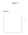
- FIG. 7 is a schematic view illustrating a bulk-type touch electrode in the organic light-emitting display panel having a built-in touchscreen according to exemplary embodiments
- FIG. 8 and FIG. 9 are schematic views illustrating a mesh-type touch electrode in the organic light-emitting display panel having a built-in touchscreen according to exemplary embodiments
- FIG. 10 is a cross-sectional view illustrating the organic light-emitting display panel having a built-in touchscreen according to exemplary embodiments
- FIG. 11 is a schematic view illustrating a color filter-on-encapsulation layer (COE) structure of the organic light-emitting display panel having a built-in touchscreen according to exemplary embodiments;
- COE color filter-on-encapsulation layer
- FIG. 12 is a schematic view illustrating a touch sensor-on-encapsulation layer (TOE) structure of the organic light-emitting display panel having a built-in touchscreen according to exemplary embodiments;
- TOE touch sensor-on-encapsulation layer
- FIG. 13 is a schematic view illustrating a M-TOE structure of the organic light-emitting display panel having a built-in touchscreen according to exemplary embodiments;
- FIG. 14 and FIG. 15 are plan views illustrating organic light-emitting display panels having a built-in touchscreen and a M-TOE structure according to exemplary embodiments;
- FIG. 16 is a schematic view illustrating a first COE and M-TOE combination structure in the organic light-emitting display panel having a built-in touchscreen according to exemplary embodiments;
- FIG. 17 is a cross-sectional view illustrating the first COE and M-TOE combination structure in the organic light-emitting display panel having a built-in touchscreen according to exemplary embodiments;
- FIG. 18 is a schematic view illustrating the process steps of fabricating the first COE and M-TOE combination structure in the organic light-emitting display panel having a built-in touchscreen according to exemplary embodiments;
- FIG. 19 is a schematic view illustrating a second COE and M-TOE combination structure in the organic light-emitting display panel having a built-in touchscreen according to exemplary embodiments;
- FIG. 20 is a cross-sectional view illustrating a second COE and M-TOE combination structure in the organic light-emitting display panel having a built-in touchscreen according to exemplary embodiments;
- FIG. 21 is a schematic view illustrating the process steps of fabricating the second COE and M-TOE combination structure in the organic light-emitting display panel having a built-in touchscreen according to exemplary embodiments;
- FIG. 22 is a schematic view illustrating the distance defined between the touch electrode and the second electrode and a parasitic capacitance component formed between the touch electrode and the second electrode in the organic light-emitting display panel having a built-in touchscreen according to exemplary embodiments;
- FIG. 23 is a schematic view illustrating the distance between the touch electrode TE and the second electrode in the organic light-emitting display panel having a built-in touchscreen and a first COE and M-TOE combination structure;
- FIG. 24 is a schematic view illustrating the distance between the touch electrode and the second electrode in the organic light-emitting display panel having a built-in touchscreen and a second COE and M-TOE combination structure;
- FIG. 25 is a graph illustrating RC delay and touch sensing performance according to the distance between the touch electrode and the second electrode in the organic light-emitting display panel having a built-in touchscreen according to exemplary embodiments.
- FIG. 26 is a schematic view illustrating load-free driving for removing a parasitic capacitance component from the organic light-emitting display device having a built-in touchscreen according to exemplary embodiments.
- FIG. 1 is a schematic view illustrating the configuration of an organic light-emitting display device 100 having a built-in touchscreen according to exemplary embodiments.
- the organic light-emitting display device 100 having a built-in touchscreen can perform a display function to display images and a touch sensing function to sense a touch made using a pointer, such as a finger or a stylus.
- the organic light-emitting display device 100 having a built-in touchscreen may operate in a display mode to perform the display function in a display mode section while operating in a touch mode to perform the touch sensing function in a touch mode section.
- the display mode section and the touch mode section may be divided on a temporal basis, may be simultaneous within the same period of time, or may overlap on a temporal basis.
- the display mode operation for displaying images and the touch mode operation for performing touch sensing can be performed separately or simultaneously.
- the organic light-emitting display device 100 having a built-in touchscreen includes an organic light-emitting display panel 110 having a built-in touchscreen, a display driving circuit, and a touch sensing circuit TSC.
- a plurality of subpixels SP defined by a plurality of data lines DL and a plurality of gate lines GL are arranged and a plurality of touch electrodes TE are disposed on the organic light-emitting display panel 110 having a built-in touchscreen.
- the display driving circuit drives the organic light-emitting display panel 110 having a built-in touchscreen to perform the display function.
- the touch sensing circuit TSC drives the organic light-emitting display panel 110 having a built-in touchscreen to perform the touch sensing function.
- the display driving circuit includes a data driving circuit DDC to drive the plurality of data lines DL and a gate driving circuit GDC to drive the plurality of gate lines GL in the display mode section.
- the display driving circuit may further include at least one controller to control the operation timing of the data driving circuit DDC and the gate driving circuit GDC, the supply of power to the data driving circuit DDC and the gate driving circuit GDS, and the like.
- a touch sensing circuit TSC can supply a touch driving signal TDS to at least one touch electrode among the plurality of touch electrodes TE and determine the occurrence of a touch and/or a touched position based on a touch sensing signal TSS detected by the touch electrode TE to which the touch driving signal TDS is applied.
- the touch sensing circuit TSC includes a touch driving circuit TDC, a touch processor TP, and the like.
- the touch driving circuit TDC drives the plurality of touch electrodes TE, while the touch processor TP determines the occurrence of a touch and/or a touched position based on signals received from the touch electrodes TE to which the touch driving signals TDS are applied.
- the touch driving circuit TDC can supply the touch driving signals TDS to the plurality of touch electrodes TE to drive the plurality of touch electrodes TE.
- the touch driving circuit TDC can receive touch sensing signals TSS from the touch electrodes TE to which the touch driving signals TDS are supplied.
- the touch driving circuit TDC supplies the received touch sensing signals TSS, or sensing data obtained by processing the received touch sensing signals TSS, to the touch processor TP.
- the touch processor TP can execute a touch algorithm using the touch sensing signals TSS or the sensing data and determine the occurrence of a touch and/or the touched position by executing the touch algorithm.
- the organic light-emitting display device 100 having a built-in touchscreen uses a self-capacitance based touch sensing method that determines the occurrence of a touch and/or the touched position by detecting a change in self-capacitance between each of the touch electrodes TE and the pointer.
- the touch driving signals TDS are applied to the touch electrodes TE and the touch sensing signals TSS are detected using the touch electrodes TE.
- the organic light-emitting display device 100 having a built-in touchscreen senses a touch using the self-capacitance based touch sensing method as described above, the organic light-emitting display panel 110 having a built-in touchscreen is only required to have a self-capacitance based touch sensing structure.
- the data driving circuit DDC, the gate driving circuit GDC, the touch driving circuit TDC, and the touch processor TP as described above are categorized according to function.
- the source driving circuit SDC, the gate driving circuit GDC, the touch driving circuit TDC, and the touch processor TP may be provided separately from each other, or alternatively, two or more thereof may be integrated with each other.
- FIG. 2 is a schematic circuit diagram illustrating a subpixel structure of the organic light-emitting display panel 110 having a built-in touchscreen according to exemplary embodiments
- FIG. 3 is a schematic circuit diagram illustrating another subpixel structure of the organic light-emitting display panel 110 having a built-in touchscreen according to exemplary embodiments.
- each of the subpixels SP basically includes an organic light-emitting diode OLED; a driving transistor DRT driving the OLED; a first transistor T 1 delivering data to a first node N 1 of the driving transistor DRT corresponding to a gate node; and a storage capacitor C 1 maintaining a data voltage VDATA corresponding to an image signal voltage or a voltage corresponding to the data voltage for a period of a single frame.
- the OLED includes a first electrode (i.e. an anode or a cathode) E 1 , an organic light-emitting layer EL, and a second electrode (i.e. a cathode or an anode) E 2 .
- a base voltage EVSS is applied to the second electrode E 2 of the OLED.
- the driving transistor DRT drives the OLED by supplying driving current to the OLED.
- the driving transistor DRT has a first node N 1 , a second node N 2 , and a third node N 3 .
- the first node N 1 of the driving transistor DRT corresponding to the gate node, is electrically connected to a source node or a drain node of the first transistor T 1 .
- the second node N 2 of the driving transistor DRT is electrically connected to the first electrode E 1 of the OLED, and is a source node or a drain node.
- the third node N 3 of the driving transistor DRT is a node to which a driving voltage EVDD is applied, is electrically connected to a driving voltage line DVL through which the driving voltage EVDD is supplied, and is a drain node or a source node.
- the driving transistor DRT and the first transistor T 1 may be embodied as n-type transistors or p-type transistors.
- the first transistor T 1 is electrically connected between a data line DL and the first node N 1 of the driving transistor DRT, and is controlled by a scanning signal SCAN applied to the gate node thereof through a gate line.
- the first transistor T 1 is turned on by the scanning signal SCAN to deliver the data voltage VDATA, supplied through the data line DL, to the first node of the driving transistor.
- the storage capacitor C 1 is electrically connected between the first node N 1 and the second node N 2 of the driving transistor DRT.
- the storage capacitor C 1 is an external capacitor intentionally designed to be disposed outside of the driving transistor DRT, instead of being a parasitic capacitor Cgs or Cgd, i.e. an internal capacitor present between the first node N 1 and the second node N 2 of the driving transistor DRT.
- each of the subpixels SP disposed on the organic light-emitting display panel further includes a second transistor T 2 , in addition to the OLED, the driving transistor DRT, the first transistor T 1 , and the storage capacitor C 1 .
- the second transistor T 2 is electrically connected between the second node N 2 of the driving transistor DRT and a reference voltage line RVL through which a reference voltage VREF is supplied, and is controlled by a sensing signal SENSE, a type of scanning signal, supplied to the gate node thereof.
- the second transistor T 2 is further provided, it is possible to more effectively control the status of the voltage of the second node N 2 of the driving transistor DRT of the subpixel SP.
- the second transistor T 2 is turned on by the sensing signal SENSE to apply the reference voltage VREF, supplied through the reference voltage line RVL, to the second node N 2 of the driving transistor DRT.
- the subpixel structure illustrated in FIG. 3 is advantageous for accurately initializing the voltage of the second node N 2 of the driving transistor DRT and sensing the unique characteristics (e.g. the threshold voltage or the degree of mobility) of the driving transistor DRT and the unique characteristics (e.g. the threshold voltage) of the OLED.
- the scanning signal SCAN and the sensing signal SENSE may be separate gate signals.
- the scanning signal SCAN and the sensing signal SENSE may be applied to the gate node of the first transistor T 1 and the gate node of the second transistor T 2 , respectively, through different gate lines.
- the scanning signal SCAN and the sensing signal SENSE may be identical signals.
- the scanning signal SCAN and the sensing signal SENSE may be commonly applied to the gate node of the first transistor T 1 and the gate node of the second transistor T 2 .
- a touchscreen building-in structure allowing a touchscreen to be built in an organic light-emitting display panel that can have the above-described subpixel structure, as well as an integrated driving method, an integrated driving circuit, and a signal connecting structure associated with the touchscreen building-in structure, will be described.
- an encapsulation layer may be disposed on the second electrode E 2 to prevent moisture, air, or the like from infiltrating thereinto.
- FIG. 4 is a schematic view illustrating display driving patterns in the organic light-emitting display panel 110 having a built-in touchscreen according to exemplary embodiments.
- each of the subpixels SP may have the subpixel structure illustrated in FIG. 2 or FIG. 3 , and in a display mode section, may be driven by a single data line DL and one or more gate lines GL.
- Data pads DP are connected to ends of the data lines DL to electrically connect the data lines DL to the data driving circuit DDC.
- the size of a single touch electrode TE may be the same as the size of a single subpixel SP, the size of the single touch electrode TE may be greater than the size of a single subpixel SP in regard of the degrees of efficiency of touch driving and touch sensing.
- FIG. 5 is a schematic view illustrating touch sensing patterns in the organic light-emitting display panel 110 having a built-in touchscreen according to exemplary embodiments.
- touch sensing patterns including a plurality of touch electrodes TE, a plurality of touch lines TL, and a plurality of touch pads TP, are disposed on the organic light-emitting display panel 110 having a built-in touchscreen according to exemplary embodiments.
- each of the touch electrodes TE acts as both a driving electrode and a receiving electrode (i.e. a sensing electrode).
- the plurality of touch electrodes TE are respectively electrically isolated from each other.
- the plurality of touch electrodes TE do not overlap each other.
- the plurality of touch lines TL are signal lines electrically connecting the plurality of touch electrodes TE to the touch sensing circuit TSC.
- the plurality of touch pads TP are disposed on predetermined ends of the plurality of touch lines TL and are electrically connected to the touch sensing circuit TSC.
- FIG. 6 is a schematic view illustrating a single touch electrode among the plurality of touch electrodes TE in the organic light-emitting display panel 110 having a built-in touchscreen according to exemplary embodiments.
- the single touch electrode TE has a touch driving signal TDS supplied through a single touch line TL.
- a single subpixel SP operates using a data voltage VDATA supplied through a single data line DL, as well as scanning signals supplied through one or more gate lines GL depending on the structure of the subpixel.
- the size of each of the plurality of touch electrodes TE is greater than the size of each of the plurality of subpixels SP.
- the size of a single touch electrode TE may be greater than the size of two subpixels SP.
- two or more gate lines GL or two or more data lines DL may be disposed in an area occupied by each of the touch electrodes TE.
- the plurality of the touch electrodes may be reduced. Accordingly, the number of instances of touch driving in which touch driving signals TDS are supplied to the touch electrodes TE may be reduced or sensing data may be reduced, whereby the efficiency of touch sensing may be improved.
- the efficiency of touch sensing may be improved due to reduced sensing data, but the accuracy of touch sensing may be reduced.
- the number and size of the touch electrodes must be accurately set in consideration of the efficiency and accuracy of touch sensing.
- touch driving signals TDS supplied to one or more touch electrodes among the touch electrodes TE or the entirety of the touch electrodes TE may be pulse-type signals.
- the touch driving signals TDS may be pulse-type signals having a waveform, for example, a spherical wave, a sine wave, or a triangular wave.
- the touch driving signals TDS may have a predetermined wavelength, phase, amplitude, or the like.
- FIG. 7 is a schematic view illustrating a bulk-type touch electrode TE in the organic light-emitting display panel 110 having a built-in touchscreen according to exemplary embodiments.
- each of the plurality of touch electrodes TE may be a bulk-type touch electrode without an open area (OA in FIG. 8 ).
- the touch electrodes TE are bulk-type touch electrodes
- the touch electrodes TE may be transparent electrodes.
- the touch electrodes TE are formed as bulk-type electrodes without an open area OA as described above, the touch electrodes TE can be easily patterned.
- the touch electrodes TE are embodied as transparent electrodes, the touch electrodes TE without an influence on luminescent performance in subpixel areas can be formed on the organic light-emitting display panel 110 having a built-in touchscreen.
- FIG. 8 and FIG. 9 are schematic views illustrating a mesh-type touch electrode TE in the organic light-emitting display panel 110 having a built-in touchscreen according to exemplary embodiments.
- each of the plurality of touch electrodes TE may be a mesh-type touch electrode having open areas OA.
- the touch electrodes TE may be transparent or opaque electrodes.
- each of the open areas OA corresponds to a light-emitting area of each subpixel. That is, the first electrode E 1 of each subpixel is located in each open area OA.
- the mesh-type touch electrodes TE or the open areas OA thereof may be diamond shaped, depending on the shape of the arrangement of the subpixels.
- the mesh-type touch electrodes TE or the open areas OA thereof may be rectangular, depending on the shape of the arrangement of the subpixels.
- the mesh-type touch electrodes TE or the open areas OA thereof may have a variety of shapes depending on the shape of the subpixels, rather than being diamond shaped or rectangular.
- the touch electrodes TE that are suitable for the structure and shape of the subpixels without reducing the luminescent efficiency of the subpixels can be formed on the organic light-emitting display panel 110 having a built-in touchscreen.
- FIG. 10 is a cross-sectional view illustrating the organic light-emitting display panel 110 having a built-in touchscreen according to exemplary embodiments.
- the cross-sectional structure of the organic light-emitting display panel 110 having a built-in touchscreen will be described with reference to FIG. 10 .
- a polyimide (PI) layer L 02 is located on a substrate or a back plate L 01 .
- a buffer layer L 03 is located on the polyimide layer L 02 , and an interlayer insulating film L 04 is located on the buffer layer L 03 .
- a gate layer L 05 is located on the interlayer insulating film L 04 , and gate electrodes or the like may be formed in desired positions on the gate layer L 05 .
- a gate insulating film L 06 is located on the gate layer L 05 .
- a source/drain layer L 07 is located on the gate insulating film L 06 .
- Signal lines such as data lines DL and link lines GL, and the source/drain electrodes of a variety of transistors may be formed on the source/drain layer L 07 .
- a protective layer L 08 is located on the source/drain layer L 07 .
- a planarization layer L 09 is located on the protective layer L 08 , and a first electrode layer L 10 is located on the planarization layer L 09 .
- the first electrode layer L 10 has first electrodes E 1 formed in light-emitting positions of subpixels.
- a bank layer L 11 is located on the first electrode layer L 10 , and an organic light-emitting layer L 12 is located on the bank layer L 11 .
- a second electrode layer L 13 is located on the organic light-emitting layer L 12 .
- the second electrode layer L 13 is formed commonly in the entirety of subpixel areas.
- An encapsulation layer L 14 for preventing the infiltration of moisture, air, and the like is located on the second electrode layer L 13 .
- a dam stacked to be higher than surrounding portions to prevent the encapsulation layer L 14 from collapsing may be provided on the peripheral portions of the panel.
- the encapsulation layer L 14 may be a single layer or may be comprised of two or more layers stacked on each other.
- the encapsulation layer L 14 may be a metal layer or may have a multilayer structure in which two or more layers comprised of organic and inorganic layers are stacked on each other.
- the encapsulation layer L 14 is a multilayer structure comprised of a first encapsulation layer L 14 a , a second encapsulation layer L 14 b , and a third encapsulation layer L 14 c.
- Each of the first encapsulation layer L 14 a , the second encapsulation layer L 14 b , and the third encapsulation layer L 14 c may be an organic layer and/or an inorganic layer.
- the thickness of the encapsulation layer L 14 may be determined in consideration of encapsulation performance.
- the thickness of the encapsulation layer L 14 may have an effect on resistor-capacitor (RC) delay and touch sensing performance (touch sensitivity) with regard to touch driving and touch sensing.
- RC resistor-capacitor
- the thickness of the encapsulation layer L 14 must be determined in consideration of RC delay and touch sensing performance (touch sensitivity).
- the organic light-emitting display panel 110 having a built-in touchscreen has a color filter-on-encapsulation layer (COE) structure in which a color filter layer is located on the encapsulation layer L 14 and a touch sensor-on-encapsulation layer (TOE) structure in which touch sensor metals, such as touch electrodes TE and touch lines TL, are located on the encapsulation layer L 14 .
- COE color filter-on-encapsulation layer
- TOE touch sensor-on-encapsulation layer
- FIG. 11 is a schematic view illustrating a COE structure of the organic light-emitting display panel 110 having a built-in touchscreen according to exemplary embodiments.
- the organic light-emitting display panel 110 having a built-in touchscreen has an encapsulation layer L 14 to prevent the organic materials of OLEDs from being exposed to oxygen, moisture, or the like.
- the encapsulation layer L 14 may be located on second electrodes E 2 of the OLEDs commonly disposed in the area in which the entirety of subpixels SP are arranged.
- the organic light-emitting display panel 110 having a built-in touchscreen further includes a color filter layer CFL located to correspond to the first electrode E 1 of the OLED.
- the color filter layer CFL converts white light generated by the organic light-emitting layer EL into light having a different color.
- a red color filter, a green color filter, and a blue color filter may be formed.
- the color filter layer CFL is located on the encapsulation layer L 14 .
- This structure is referred to as the COE structure.
- FIG. 12 is a schematic view illustrating a TOE structure of the organic light-emitting display panel 110 having a built-in touchscreen according to exemplary embodiments.
- a touch driving signal TDS is supplied to at least one touch electrode TE among the plurality of touch electrodes TE corresponding to touch sensors disposed in the organic light-emitting display panel 110 having a built-in touchscreen according to exemplary embodiments.
- the touch electrode TE to which the touch driving signal TDS is applied can form capacitance (self-capacitance) together with a pointer corresponding to a touch operation means of a user.
- the plurality of touch electrodes TE of the touch sensor metals are located on the encapsulation layer L 14 .
- This structure is referred to as the TOE structure.
- the organic light-emitting display panel 110 having a built-in touchscreen is designed to have the COE structure as described above, it is possible to improve luminescent efficiency, and in some cases, omit a circular polarizer.
- the use of the TOE structure can realize the organic light-emitting display panel 110 having a built-in touchscreen able to provide a touch sensing function without a problem in a display function.
- the touchscreen can be built in the organic light-emitting display panel 110 without making panel fabrication processing complicated.
- the touch sensor metals further include the plurality of touch lines TL through which the plurality of touch electrodes TE are electrically connected to the touch sensing circuit TSC, in addition to the plurality of touch electrodes TE.
- the plurality of touch lines TL are also located on the encapsulation layer L 14 .
- the touch lines TL through which the plurality of touch electrodes TE are electrically connected to the touch sensing circuit TSC, are disposed on the encapsulation layer L 14 as described above, signal transmission for touch driving and touch sensing can be efficiently performed.
- FIG. 13 is a schematic view illustrating a multiple touch sensor metal layer-on-encapsulation layer (M-TOE) structure of the organic light-emitting display panel 110 having a built-in touchscreen according to exemplary embodiments.
- M-TOE metal layer-on-encapsulation layer
- touch sensor metals include a number of touch electrodes TE, a plurality of touch lines TL, and the like.
- the number of touch electrodes TE and the plurality of touch lines TL may be disposed in different layers.
- the plurality of touch lines TL are disposed in a first touch sensor metal layer (TSML 1 ), while the number of touch electrodes TE are disposed in a second touch sensor metal layer (TSML 2 ).
- the plurality of touch lines TL may be disposed in the second touch sensor metal layer (TSML 2 ), while the number of touch electrodes TE may be disposed in the first touch sensor metal layer (TSML 1 ).
- the plurality of touch lines TL are electrically connected to the number of touch electrodes TE such that there is one-to-one correspondence between the touch lines TL and the touch electrodes TE.
- each of the touch lines TL is electrically connected to a respective touch electrode TE corresponding thereto through a contact hole extending through an insulation layer, but is electrically isolated from the other touch electrodes through the insulation layer.
- the TOE structure in which the number of touch electrodes TE and the plurality of touch lines TL are disposed in different touch sensor metal layers TSML 1 and TSML 2 on the same encapsulation layer L 14 is referred to as the M-TOE structure.
- the organic light-emitting display panel 110 having a built-in touchscreen is designed to have the M-TOE structure as described above, the touch electrodes TE and the touch lines TL that must be electrically isolated from each other can be accurately disconnected.
- FIG. 14 and FIG. 15 are plan views illustrating the organic light-emitting display panels 110 having a built-in touchscreen according to exemplary embodiments in which the M-TOE structure is used.
- FIG. 14 illustrates a case in which the touch electrodes TE are mesh-type touch electrodes having open areas.
- Two or more subpixels SP may be disposed below each of the touch electrodes TE.
- each of the touch electrodes TE must not block light emitted from two or more underlying subpixels SP.
- each of the open areas corresponds to each light-emitting area of the subpixels SP.
- the touch electrodes TE When the touch electrodes TE are mesh-type touch electrodes having open areas, the touch electrodes TE may be transparent electrodes or opaque electrodes.
- FIG. 15 illustrates a case in which the touch electrodes TE are bulk-type touch electrodes without open areas.
- Two or more subpixels SP may be disposed below each touch electrode TE.
- the touch electrode TE must not block light emitted from the two or more underlying subpixels SP.
- the touch electrodes TE when the touch electrodes TE are bulk-type touch electrodes without open areas, the touch electrodes TE may be transparent electrodes.
- each of the plurality of touch lines TL is electrically connected to one touch electrode TE among the number of touch electrodes TE.
- Each of the plurality of touch lines TL must be electrically connected to a specific touch electrode and must not be electrically connected to the other touch electrodes.
- the first touch sensor metal layer TSML 1 in which the plurality of touch lines TL are disposed, overlap the second touch sensor metal layer TSML 2 , in which the plurality of touch electrodes TE are disposed.
- Each of the plurality of touch lines TL overlaps at least one touch electrode among the plurality of touch electrodes TE.
- the different types of touch sensor metals TE and TL disposed to overlap as described above can reduce peripheral areas (i.e. bezel areas) in which the touch sensor metals TE and TL are not disposed.
- each of the touch lines TL extends to a touch electrode TE electrically connected thereto.
- the touch lines TL may extend to the periphery of the display panel.
- each of the plurality of touch lines TL overlaps at least one touch electrode among the plurality of touch electrodes TE in the top-bottom direction
- the plurality of touch lines TL and the plurality of touch electrodes TE corresponding to the touch sensor metals are disposed in different touch sensor metal layers TSML 1 and TSML 2 , whereby each touch line TL can be electrically isolated from non-corresponding touch electrodes TE.
- each of the plurality of touch lines TL overlaps at least one touch electrode among the plurality of touch electrodes TE
- the plurality of touch lines TL are located in a different layer from the plurality of touch electrodes TE, whereby each touch line TL can be electrically connected to a touch electrode among the plurality of touch electrodes TE corresponding thereto without being electrically isolated from the non-corresponding touch electrodes TE.
- the touch sensor metals can operate ordinarily, whereby touch sensing can be performed ordinarily.
- the plurality of touch lines TL corresponding to the touch sensor metals are electrically isolated from each other. Furthermore, the plurality of touch lines TL do not overlap each other.
- the plurality of touch electrodes TE corresponding to the touch sensor metals are electrically isolated from each other. Furthermore, the plurality of touch electrodes TE do not overlap each other.
- each touch electrode TE is connected to a corresponding touch line TL through a contract hole.
- a bridge a portion in which each touch electrode TE is connected to a corresponding touch line TL through a contract hole.
- FIG. 16 is a schematic view illustrating a first COE and M-TOE combination structure in the organic light-emitting display panel 110 having a built-in touchscreen according to exemplary embodiments.
- the first touch sensor metal layer TSML 1 in which first touch sensor metals that may be the plurality of touch lines TL are located, is separated from the second touch sensor metal layer TSML 2 , in which second touch sensor metals that may be the plurality of touch electrodes TE are located, by an insulation layer IL.
- Each of the touch lines TL is electrically connected to a respective touch electrode TE corresponding thereto, through a contact hole (located in a bridge) extending through the insulation layer IL.
- the first touch sensor metal layer TSML 1 , insulation layer IL, and the second touch sensor metal layer TSML 2 form a built-in touchscreen panel.
- the first touch sensor metal layer TSML 1 , insulation layer IL, and the second touch sensor metal layer TSML 2 are disposed between the encapsulation layer L 14 and the color filter layer CFL.
- the encapsulation layer L 14 , the built-in touchscreen panel TSML 1 , IL, and TSML 2 , and the color filter layer CFL are sequentially layered.
- the color filter layer CFL is located outward of the built-in touchscreen panel TSML 1 , IL, and TSML 2 as described above, light that has been color-converted in the color filter layer CFL can be prevented from being distorted in the built-in touchscreen TSML 1 , IL, and TSML 2 . It is therefore possible to reduce the influence of the touch sensing structure on display performance.
- FIG. 17 is a cross-sectional view illustrating the first COE and M-TOE combination structure in the organic light-emitting display panel 110 having a built-in touchscreen according to exemplary embodiments.
- an overcoat layer OCL is disposed between the encapsulation layer L 14 and the color filter layer CFL comprised of a plurality of patterned color filters CF.
- each of the subpixels SP may have a color filter CF disposed therein, the color of the color filter CF corresponding to the color of the subpixel.
- red color filters CF _ R when subpixels generating red light, subpixels generating green light, and subpixels generating blue light are disposed in the organic light-emitting display panel 110 having a built-in touchscreen, red color filters CF _ R, green color filters CF _ G, and blue color filters CF _ B are disposed in the color filter layer CFL.
- Black matrices BM may be respectively located between two adjacent subpixels SP.
- the plurality of touch electrodes TE and the plurality of touch lines TL are disposed between the encapsulation layer L 14 and the overcoat layer OCL.
- FIG. 17 illustrates a single touch electrode among the plurality of mesh-type touch electrodes TE illustrated in FIG. 14 , the single touch electrode TE being closest to a touch pad TP, and a single touch line TL electrically connected to the single mesh-type touch electrode TE through a contact hole in the bridge.
- the positions of the open areas of the mesh-type touch electrodes TE illustrated in FIG. 17 correspond to the positions of the light-emitting areas of the subpixels.
- the positions of the light-emitting areas of the subpixels correspond to the positions of the first electrodes E 1 of the subpixels, as well as the positions of the color filters CF corresponding to the subpixels.
- the first touch sensor metal layer TSML 1 in which the plurality of touch lines TL are disposed, the insulation layer IL, and the second touch sensor metal layer TSML 2 in which the plurality of touch electrodes TE are disposed, are disposed between the encapsulation layer L 14 and the overcoat layer OCL.
- the built-in touchscreen panel including the first touch sensor metal layer TSML 1 , the insulation layer IL, and second touch sensor metal layer TSML 2 , is disposed between the encapsulation layer L 14 and the overcoat layer OCL.
- the plurality of touch lines TL are disposed in the first touch sensor metal layer TSML 1 on the encapsulation layer L 14 .
- the insulation layer IL is disposed on the first touch sensor metal layer TSML 1 .
- the plurality of touch electrodes TE are disposed in the second touch sensor metal layer TSML 2 on the insulation layer IL.
- the overcoat layer OCL is disposed on the second touch sensor metal layer TSML 2 .
- the touch pads TP are located on the outer ends of the plurality of touch lines TL, respectively, in the first touch sensor metal layer TSML 1 , and are electrically connected to the touch sensing circuit TSC.
- FIG. 18 is a schematic view illustrating the process steps of fabricating the first COE and M-TOE combination structure in the organic light-emitting display panel 110 having a built-in touchscreen according to exemplary embodiments.
- a built-in touchscreen panel is fabricated on the encapsulation layer L 14 .
- the touch lines TL are disposed on the first touch sensor metal layer TSML 1 on the encapsulation layer L 14 .
- the outer ends of the touch lines TL may act as the touch pads TP electrically connected to the touch sensing circuit TSC.
- An insulation layer IL is formed on the first touch sensor metal layer TSML 1 , and the plurality of touch electrodes TE are formed on the insulation layer IL to be located in the second touch sensor metal layer TSML 2 .
- the encapsulation layer L 14 on which the built-in touchscreen panel is fabricated is covered with an overcoat layer OCL.
- black matrices BM are formed on the overcoat layer OCL, in positions corresponding to the boundaries of the subpixels
- the color filters CF corresponding to the light-emitting areas of the subpixels are patterned.
- the overcoat layer OCL is formed on the touch sensor metals, such as the touch lines TL, and the touch pads TP, and the touch electrodes TE, as described above, it is possible to protect the touch sensor metals TE and TL using the overcoat layer OCL.
- FIG. 19 is a schematic view illustrating a second COE and M-TOE combination structure in the organic light-emitting display panel 110 having a built-in touchscreen according to exemplary embodiments.
- the touch sensor metals including the plurality of touch electrodes TE and the plurality of touch lines TL, are disposed on the color filter layer CFL.
- the encapsulation layer L 14 , the color filter layer CFL, and the touch sensor metals TE, TL, and TP are sequentially layered.
- the first touch sensor metal layer TSML 1 in which the plurality of touch lines TL are disposed is located on the color filter layer CFL, which is disposed on the encapsulation layer L 14 .
- the insulation layer IL is located on the first touch sensor metal layer TSML 1 in which the plurality of touch lines TL are disposed, and the second touch sensor metal layer TSML 2 in which the plurality of touch electrodes TE are disposed is located on the insulation layer IL.
- the first touch sensor metal layer TSML 1 in which the plurality of touch lines TL are disposed, the insulation layer IL, the second touch sensor metal layer TSML 2 in which the plurality of touch electrodes TE are disposed correspond to the built-in touchscreen panel disposed within the organic light-emitting display panel 110 .
- the touch sensor metals e.g. the touch electrodes TE
- the distance between the touch pointer of the user to a touch electrode TE corresponding thereto may be reduced, thereby increasing the level of capacitance between the pointer and the corresponding touch electrode TE. Consequently, the accuracy of the operation of sensing a touch and a touched position can be improved.
- FIG. 20 is a cross-sectional view illustrating a second COE and M-TOE combination structure in the organic light-emitting display panel having a built-in touchscreen according to exemplary embodiments.
- the overcoat layer OCL is further disposed on the color filter layer CFL formed by patterning a plurality of color filters CF on the encapsulation layer L 14 .
- each of the subpixels SP may have a color filter CF disposed therein, the color of the color filter CF corresponding to the color of the subpixel.
- red color filters CF _ R when subpixels generating red light, subpixels generating green light, and subpixels generating blue light are disposed in the organic light-emitting display panel 110 having a built-in touchscreen, red color filters CF _ R, green color filters CF _ G, and blue color filters CF _ B are disposed in the color filter layer CFL.
- Black matrices BM may be respectively located between two adjacent subpixels SP.
- the overcoat layer OCL is disposed on the color filters CF.
- the touch sensor metals including the plurality of touch electrodes TE, the plurality of touch lines TL, and the plurality of touch pads TP, are disposed on the overcoat layer OCL.
- the first touch sensor metal layer TSML 1 in which the plurality of touch lines TL are disposed, the insulation layer IL, and the second touch sensor metal layer TSML 2 in which the plurality of touch electrodes TE are disposed are disposed on the overcoat layer OCL.
- the touch pads TP that may be connected to the touch lines TL or may be portions of the touch lines TL are located in the first touch sensor metal layer TSML 1 .
- the touch electrodes TE located in the second touch sensor metal layer TSML 2 are electrically connected to the touch lines TL, located in the first touch sensor metal layer TSML 1 , through contact holes in the bridge area.
- FIG. 20 illustrates a single mesh-type touch electrode among the plurality of mesh-type touch electrodes TE illustrated in FIG. 14 , the single touch electrode TE being closest to a touch pad TP, and a single touch line TL electrically connected to the single mesh-type touch electrode TE through a contact hole in the bridge.
- the positions of the mesh-type touch electrodes TE illustrated in FIG. 20 correspond to the positions of the light-emitting areas of the subpixels.
- the positions of the light-emitting areas of the subpixels correspond to the positions of the first electrodes E 1 of the subpixels, as well as the positions of the color filters CF corresponding to the subpixels.
- FIG. 21 is a schematic view illustrating the process steps of fabricating the second COE and M-TOE combination structure in the organic light-emitting display panel 110 having a built-in touchscreen according to exemplary embodiments.
- the black matrices BM are formed on boundaries of the subpixels.
- the color filters CF corresponding to the light-emitting areas of the subpixels are patterned.
- the encapsulation layer L 14 with the color filters CF and the black matrices BM patterned thereon, is covered with the overcoat layer OCL.
- a built-in touchscreen panel is formed on the overcoat layer OCL.
- the touch electrodes TE, the touch lines TL, and the touch pads TP corresponding to the touch sensor metals forming the built-in touchscreen panel are formed on the overcoat layer OCL.
- the touch lines TL are located in the first touch sensor metal layer TSML 1 on the overcoat layer OCL, the insulation layer IL is located on the first touch sensor metal layer TSML 1 , and the touch electrodes TE are located in the second touch sensor metal layer TSML 2 on the insulation layer IL.
- the touch electrodes TE located in the second touch sensor metal layer TSML 2 are electrically connected to the touch lines TL, located in the first touch sensor metal layer TSML 1 , through the contact holes in the bridge area.
- the touch pads TP connected to the touch lines TL or the touch pads TP corresponding to portions of the touch lines TL are located in the first touch sensor metal layer TSML 1 .
- the overcoat layer OCL is formed on the color filter layer CFL, and the touch sensor metals TE, TL, and TP are formed on the overcoat layer OCL. It is thereby possible to protect the color filter layer CFL and the patterns below the color filter layer CFL using the overcoat layer OCL.
- the overcoat layer OCL can prevent the touch electrodes TE, the touch lines TL, and the like from electrically interfering with electrodes, voltage lines, or signal lines located below the overcoat layer OCL.
- FIG. 22 is a schematic view illustrating the distance T defined between the touch electrode TE and the second electrode E 2 and a parasitic capacitance component formed between the touch electrode TE and the second electrode E 2 in the organic light-emitting display panel 110 having a built-in touchscreen according to exemplary embodiments.
- a touch driving signal TDS is applied to the touch electrode TE.
- a base voltage EVSS is applied to the second electrode E 2 (e.g. cathode) of the OLED.
- the base voltage EVSS may be a DC voltage having a ground voltage value or a specific voltage value.
- the encapsulation layer L 14 is disposed between the touch electrode TE and the second electrode E 2 of the OLED.
- the encapsulation layer L 14 is disposed between the touch electrode TE and the second electrode E 2 of the OLED.
- the encapsulation layer L 14 and the overcoat layer OCL are disposed between the touch electrode TE and the second electrode E 2 of the OLED.
- parasitic capacitance Cpara may be formed between the touch electrode TE to which the touch driving signal TDS is applied and the second electrode E 2 to which the base voltage EVSS is applied.
- the parasitic capacitance Cpara acts as a load increasing RC delay regarding the touch electrode TE and the touch line TL.
- the parasitic capacitance Cpara may change sensing data obtained from a signal received from the touch electrode TE to which the touch driving signal TDS is applied, thereby forming a touch sensing error.
- the organic light-emitting display panel 110 having a built-in touchscreen may have a structural feature able to prevent the parasitic capacitance Cpara. This feature will be described with reference to FIG. 23 , FIG. 24 , and FIG. 25 .
- FIG. 23 is a schematic view illustrating the distance T 1 between the touch electrode TE and the second electrode E 2 in the organic light-emitting display panel 110 having a built-in touchscreen and a first COE and M-TOE combination structure
- FIG. 24 is a schematic view illustrating the distance T 2 between the touch electrode TE and the second electrode E 2 in the organic light-emitting display panel 110 having a built-in touchscreen and a second COE and M-TOE combination structure
- FIG. 25 is a graph illustrating RC delay and touch sensing performance according to the distance T between the touch electrode TE and the second electrode E 2 in the organic light-emitting display panel 110 having a built-in touchscreen according to exemplary embodiments.
- the distance T 1 between the touch electrode TE and the second electrode E 2 corresponds to the thickness of the encapsulation layer L 14 .
- the distance T 2 between the touch electrode TE and the second electrode E 2 corresponds to a total of the thickness of the encapsulation layer L 14 and the thickness of the overcoat layer OCL.
- a decrease in the distance T between the touch electrode TE and the second electrode E 2 increases the parasitic capacitance Cpara between the second electrode E 2 and the touch electrode TE, thereby increasing RC delay and lowering touch sensing performance (touch sensitivity).
- an increase in the distance T between the touch electrode TE and the second electrode E 2 reduces the parasitic capacitance Cpara between the second electrode E 2 and the touch electrode TE, thereby decreasing RC delay and improving touch sensing performance (touch sensitivity).
- the distance T between the touch electrode TE and the second electrode E 2 must be equal to or greater than a threshold thickness T _ TH corresponding to maximum allowable RC delay KD and minimum touch sensing performance KP.
- the encapsulation layer L 14 must be formed to be relatively thick, such that the distance T 1 between the touch electrode TE and the second electrode E 2 is equal to or greater than the threshold thickness T _ TH.
- the encapsulation layer L 14 and the overcoat layer OCL must be formed to be relatively thick such that the distance T 2 between the touch electrode TE and the second electrode E 2 is equal to or greater than the threshold thickness T _ TH.
- the distance T 1 between the touch electrode TE and the second electrode E 2 in the organic light-emitting display panel 110 having a built-in touchscreen in which the first COE and M-TOE combination structure illustrated in FIG. 23 is provided or the distance T 2 between the touch electrode TE and the second electrode E 2 in the organic light-emitting display panel 110 having a built-in touchscreen in which the second COE and S-TOE combination structure illustrated in FIG. 24 is provided may be equal to the distance between the plurality of touch electrodes TE and the bottom surface of the encapsulation layer L 14 (i.e. the top surface of the second electrode E 2 ).
- the threshold thickness T _ TH may be 5 ⁇ m.
- the distance between the plurality of touch electrodes TE and the bottom surface of the encapsulation layer L 14 may be designed to be equal to or greater than 5 ⁇ m.
- each of the high-resistance black matrices BM is disposed between two adjacent color filters among the color filters CF in the color filter layer CFL.
- the resistance of the high-resistance black matrices BM is equal to or higher than a predetermined level of resistance.
- the touch sensor metals can be reliably disposed within the organic light-emitting display panel 110 including an organic material.
- the distance between the second electrode E 2 and the touch electrode TE (i.e. the distance between the bottom surface of the encapsulation layer L 14 and the touch electrode TE) is designed to be equal to or greater than a predetermined value T _ TH of, for example, 5 ⁇ m, whereby the parasitic capacitance Cpara can be prevented from being formed between the second electrode E 2 and the touch electrode TE.
- the structural design change (e.g. the changed thickness) can prevent the parasitic capacitance Cpara from being formed between the second electrode E 2 and the touch electrode TE.
- load-free driving performed during the touch mode section can prevent the parasitic capacitance Cpara from being formed between the second electrode E 2 and the touch electrode TE.
- FIG. 26 is a schematic view illustrating load-free driving for removing a parasitic capacitance component from the organic light-emitting display device 100 having a built-in touchscreen according to exemplary embodiments.
- the organic light-emitting display device 100 having a built-in touchscreen performs load-free driving of applying a load-free driving signal LFDS to the second electrode E 2 to reduce the potential difference between the second electrode E 2 and the touch electrode TE, thereby being able to prevent parasitic capacitance Cpara from being formed between the second electrode E 2 and the touch electrode TE.
- the load-free driving signal LFDS may be a signal identical to the touch driving signal TDS or a signal corresponding to the touch driving signal TDS.
- At least one of the frequency, phase, and amplitude of the load-free driving signal TDS may be identical to a corresponding one of the frequency, phase, and amplitude of the touch driving signal TDS.
- the signal output characteristics of the organic light-emitting display device 100 having a built-in touchscreen can be controlled such that at least one of the frequency, phase, and amplitude of the load-free driving signal TDS becomes identical to a corresponding one of the frequency, phase, and amplitude of the touch driving signal TDS at a point at which the load-free driving signal TDS is actually applied to the second electrode E 2 and a point at which the touch driving signal TDS is actually applied to the touch electrode TE.
- the signal output characteristics of the load-free driving signal TDS and the touch driving signal TDS are controlled by a signal output configuration such that at least one of the frequency, phase, and amplitude of the load-free driving signal TDS becomes identical to a corresponding one of the frequency, phase, and amplitude of the touch driving signal TDS at the point at which the load-free driving signal TDS is actually applied to the second electrode E 2 and the point at which the touch driving signal TDS is actually applied to the touch electrode TE, at least one of the frequency, phase, and amplitude of the load-free driving signal TDS may differ from a corresponding one of the frequency, phase, and amplitude of the touch driving signal TDS at a point at which the load-free driving signal TDS and the touch driving signal TDS are output.
- the organic light-emitting display panel 110 having a built-in touchscreen and the organic light-emitting display device 100 having a built-in touchscreen are provided with a structure enabling a touchscreen panel (i.e. touch sensor metals) to be disposed therewithin.
- a touchscreen panel i.e. touch sensor metals
- the organic light-emitting display panel 110 having a built-in touchscreen and the organic light-emitting display device 100 having a built-in touchscreen can improve touch sensing performance.
- the organic light-emitting display panel 110 having a built-in touchscreen and the organic light-emitting display device 100 having a built-in touchscreen are provided with a structure enabling an ultrathin profile to be designed.
- the organic light-emitting display panel 110 having a built-in touchscreen and the organic light-emitting display device 100 having a built-in touchscreen are provided with a touchscreen panel (i.e. touch sensor metals) disposed therewithin without display performance being influenced.
- a touchscreen panel i.e. touch sensor metals
- the organic light-emitting display panel 110 having a built-in touchscreen and the organic light-emitting display device 100 having a built-in touchscreen are provided with an M-TOE structure in which two touch sensor metals (touch electrodes and touch lines) are disposed in different layers, the touch sensor metals enabling self-capacitance based touch sensing.
Landscapes
- Engineering & Computer Science (AREA)
- General Engineering & Computer Science (AREA)
- Theoretical Computer Science (AREA)
- Physics & Mathematics (AREA)
- Human Computer Interaction (AREA)
- General Physics & Mathematics (AREA)
- Computer Networks & Wireless Communication (AREA)
- Optics & Photonics (AREA)
- Electroluminescent Light Sources (AREA)
- Devices For Indicating Variable Information By Combining Individual Elements (AREA)
- Optical Filters (AREA)
Applications Claiming Priority (2)
| Application Number | Priority Date | Filing Date | Title |
|---|---|---|---|
| KR1020160122352A KR20180033360A (ko) | 2016-09-23 | 2016-09-23 | 터치스크린 내장형 유기발광표시패널 및 유기발광표시장치 |
| KR10-2016-0122352 | 2016-09-23 |
Publications (2)
| Publication Number | Publication Date |
|---|---|
| US20180088726A1 US20180088726A1 (en) | 2018-03-29 |
| US10386956B2 true US10386956B2 (en) | 2019-08-20 |
Family
ID=57629506
Family Applications (1)
| Application Number | Title | Priority Date | Filing Date |
|---|---|---|---|
| US15/391,625 Active US10386956B2 (en) | 2016-09-23 | 2016-12-27 | Organic light-emitting display panel and organic light-emitting display device having built-in touchscreen |
Country Status (6)
| Country | Link |
|---|---|
| US (1) | US10386956B2 (ja) |
| EP (1) | EP3299940B1 (ja) |
| JP (2) | JP6466394B2 (ja) |
| KR (1) | KR20180033360A (ja) |
| CN (1) | CN107871760B (ja) |
| TW (1) | TWI627570B (ja) |
Cited By (2)
| Publication number | Priority date | Publication date | Assignee | Title |
|---|---|---|---|---|
| US11061498B2 (en) * | 2016-09-30 | 2021-07-13 | Samsung Display Co., Ltd. | Display module |
| TWI746107B (zh) * | 2019-08-27 | 2021-11-11 | 聯詠科技股份有限公司 | 用於有機發光二極體觸控面板的控制方法及其驅動裝置 |
Families Citing this family (18)
| Publication number | Priority date | Publication date | Assignee | Title |
|---|---|---|---|---|
| KR102561120B1 (ko) | 2016-09-23 | 2023-07-28 | 엘지디스플레이 주식회사 | 터치스크린 내장형 유기발광표시패널 및 유기발광표시장치 |
| KR102608954B1 (ko) * | 2016-09-30 | 2023-12-05 | 삼성디스플레이 주식회사 | 표시 장치 |
| JP6885134B2 (ja) * | 2017-03-24 | 2021-06-09 | セイコーエプソン株式会社 | 電気光学装置、電気光学装置の製造方法、電子機器 |
| CN107180852B (zh) * | 2017-05-18 | 2019-11-15 | 上海天马有机发光显示技术有限公司 | 一种触控显示面板及显示装置 |
| CN107275512A (zh) * | 2017-05-25 | 2017-10-20 | 厦门天马微电子有限公司 | 一种有机电致发光显示面板、其制作方法及显示装置 |
| KR102325262B1 (ko) * | 2017-06-01 | 2021-11-10 | 엘지디스플레이 주식회사 | 터치 디스플레이 장치, 터치 디스플레이 패널 및 터치 디스플레이 패널의 제조 방법 |
| CN108470753B (zh) * | 2018-03-28 | 2021-02-26 | 京东方科技集团股份有限公司 | 一种电致发光显示面板、其制作方法及显示装置 |
| KR101918146B1 (ko) * | 2018-04-27 | 2018-11-13 | 셀로코아이엔티 주식회사 | 인셀 터치표시장치 및 그 제조방법 |
| KR102534689B1 (ko) * | 2018-06-14 | 2023-05-19 | 엘지디스플레이 주식회사 | 터치표시장치, 데이터구동회로 및 구동방법 |
| KR102575506B1 (ko) * | 2018-07-19 | 2023-09-05 | 엘지디스플레이 주식회사 | 터치 센서를 구비하는 표시장치 |
| KR102536348B1 (ko) * | 2018-07-19 | 2023-05-24 | 엘지디스플레이 주식회사 | 터치 센서를 가지는 표시 장치 |
| WO2020149139A1 (ja) * | 2019-01-16 | 2020-07-23 | 株式会社小糸製作所 | イメージング装置、その演算処理装置、車両用灯具、車両、センシング方法 |
| KR20210012216A (ko) * | 2019-07-24 | 2021-02-03 | 엘지디스플레이 주식회사 | 터치 전극들을 포함하는 디스플레이 장치 |
| KR102384388B1 (ko) * | 2019-12-18 | 2022-04-07 | 엘지디스플레이 주식회사 | 터치 디스플레이 장치 |
| KR20210084913A (ko) * | 2019-12-30 | 2021-07-08 | 엘지디스플레이 주식회사 | 유기 발광 표시 장치 |
| US10908752B1 (en) * | 2020-02-14 | 2021-02-02 | Novatek Microelectronics Corp. | Display panel with touch sensor |
| CN111509141B (zh) * | 2020-05-06 | 2023-08-01 | 上海天马微电子有限公司 | 一种显示面板及其制备方法、显示装置 |
| KR20220057767A (ko) * | 2020-10-30 | 2022-05-09 | 엘지디스플레이 주식회사 | 터치 디스플레이 장치 |
Citations (44)
| Publication number | Priority date | Publication date | Assignee | Title |
|---|---|---|---|---|
| US20100110041A1 (en) | 2008-07-11 | 2010-05-06 | Brent Jang | Organic light emitting display device |
| US20100134426A1 (en) | 2008-11-28 | 2010-06-03 | Dong-Ki Lee | Touch sensible organic light emitting device |
| JP2010181747A (ja) | 2009-02-06 | 2010-08-19 | Seiko Instruments Inc | タッチセンサ機能付液晶表示装置 |
| JP2010277461A (ja) | 2009-05-29 | 2010-12-09 | Sony Corp | タッチパネル、表示パネル、タッチパネル用基板、表示パネル用基板および表示装置 |
| JP2011023558A (ja) | 2009-07-16 | 2011-02-03 | Sharp Corp | 有機el表示装置 |
| US20120249454A1 (en) | 2011-03-31 | 2012-10-04 | Sony Corporation | Display device and electronic unit |
| WO2013018591A1 (ja) | 2011-07-29 | 2013-02-07 | シャープ株式会社 | タッチパネル基板および電気光学装置 |
| JP2013122752A (ja) | 2011-12-09 | 2013-06-20 | Lg Display Co Ltd | タッチスクリーン一体型表示装置 |
| US20140049522A1 (en) * | 2012-08-17 | 2014-02-20 | Dinesh C. Mathew | Narrow Border Organic Light-Emitting Diode Display |
| TWM480722U (zh) | 2014-01-06 | 2014-06-21 | Superc Touch Corp | 高準確度之窄邊框內嵌式平面顯示觸控結構 |
| US20140183478A1 (en) | 2012-12-27 | 2014-07-03 | Lg Display Co., Ltd. | Flexible organic light-emitting display device and method for manufacturing the same |
| JP2014211685A (ja) | 2013-04-17 | 2014-11-13 | ジオマテック株式会社 | タッチセンサ一体型表示装置 |
| TWM491878U (zh) | 2014-05-29 | 2014-12-11 | Superc Touch Corp | 以透明感應電極連接金屬走線的觸控顯示結構 |
| US20150009175A1 (en) * | 2013-07-08 | 2015-01-08 | Elo Touch Solutions, Inc. | Multi-user multi-touch projected capacitance touch sensor |
| US20150036204A1 (en) * | 2012-02-23 | 2015-02-05 | Switch Materials, Inc. | Optical filter with light source |
| US20150060817A1 (en) | 2013-08-30 | 2015-03-05 | Japan Display Inc. | Display device |
| JP2015056522A (ja) | 2013-09-12 | 2015-03-23 | 株式会社ジャパンディスプレイ | タッチパネル機能内蔵表示装置 |
| JP2015072663A (ja) | 2013-10-04 | 2015-04-16 | 株式会社ジャパンディスプレイ | 表示装置 |
| JP2015111318A (ja) | 2012-03-22 | 2015-06-18 | シャープ株式会社 | カラーフィルター一体型タッチパネル |
| WO2015088629A1 (en) | 2013-12-13 | 2015-06-18 | Pylemta Management Llc | Integrated touch and display architectures for self-capacitive touch sensors |
| JP2015143933A (ja) | 2014-01-31 | 2015-08-06 | 株式会社ジャパンディスプレイ | 静電容量型センサ付き表示装置及びその駆動方法 |
| US20150227254A1 (en) * | 2014-02-10 | 2015-08-13 | Samsung Display Co., Ltd. | Touch sensor substrate and display apparatus having the touch sensor substrate |
| JP2016004280A (ja) | 2014-06-13 | 2016-01-12 | 株式会社ジャパンディスプレイ | タッチ検出装置及びタッチ検出機能付き表示装置 |
| KR20160017336A (ko) | 2014-08-05 | 2016-02-16 | 엘지디스플레이 주식회사 | 인 셀 타입의 터치 구조를 갖는 유기발광표시장치 |
| WO2016031396A1 (ja) | 2014-08-28 | 2016-03-03 | 富士フイルム株式会社 | 加飾材付き基材、加飾層形成用転写材料、タッチパネル、及び、情報表示装置 |
| JP2016038594A (ja) | 2014-08-11 | 2016-03-22 | エルジー ディスプレイ カンパニー リミテッド | タッチセンサ一体型表示装置 |
| EP3026710A1 (en) | 2014-11-26 | 2016-06-01 | LG Display Co., Ltd. | Organic light emitting display device and fabricating method using the same |
| US20160239133A1 (en) | 2015-02-16 | 2016-08-18 | Samsung Display Co., Ltd. | Display device |
| US20160260780A1 (en) * | 2015-03-02 | 2016-09-08 | Samsung Display Co., Ltd. | Method for fabricating display device and display device |
| US20160378224A1 (en) * | 2015-06-26 | 2016-12-29 | Samsung Display Co., Ltd. | Flexible display device |
| US20170040490A1 (en) * | 2015-08-03 | 2017-02-09 | Samsung Electronics Co., Ltd. | Semiconductor light emitting device and method of manufacturing the same |
| US20170062537A1 (en) * | 2015-08-25 | 2017-03-02 | Samsung Display Co., Ltd. | Curved display device |
| US20170090634A1 (en) * | 2015-09-24 | 2017-03-30 | Lg Display Co., Ltd. | Display device including touch screen function |
| US20170102797A1 (en) * | 2015-06-18 | 2017-04-13 | X-Celeprint Limited | Display with integrated electrodes |
| US20170271617A1 (en) * | 2016-03-17 | 2017-09-21 | Samsung Display Co., Ltd. | Display device |
| US20170278901A1 (en) * | 2016-03-25 | 2017-09-28 | Samsung Display Co. , Ltd. | Display apparatus with bending area capable of minimizing manufacturing defects |
| US20170288007A1 (en) * | 2016-03-31 | 2017-10-05 | Samsung Display Co., Ltd. | Display device and manufacturing method thereof that may minimize an occurrence of a defect in the display device |
| US20170308199A1 (en) * | 2015-11-19 | 2017-10-26 | Boe Technology Group Co., Ltd. | Touch Screen and Manufacturing Method Thereof, Display Device |
| US20170323779A1 (en) * | 2016-05-03 | 2017-11-09 | Samsung Display Co., Ltd. | Display apparatus and method of manufacturing the same |
| US20180011598A1 (en) * | 2016-07-07 | 2018-01-11 | Samsung Display Co., Ltd. | Touch sensor and display device including the same |
| US20180026225A1 (en) * | 2016-07-25 | 2018-01-25 | Samsung Display Co., Ltd. | Display device with structure for preventing organic material overflow |
| US20180053905A1 (en) * | 2016-08-19 | 2018-02-22 | Samsung Display Co., Ltd. | Display apparatus |
| US9947727B2 (en) * | 2015-09-07 | 2018-04-17 | Lg Display Co., Ltd. | Organic light emitting display device and method of manufacturing the same |
| US10061432B2 (en) * | 2015-11-30 | 2018-08-28 | Lg Display Co., Ltd. | Display device having touch screen therein |
Family Cites Families (3)
| Publication number | Priority date | Publication date | Assignee | Title |
|---|---|---|---|---|
| KR101648571B1 (ko) * | 2014-07-16 | 2016-08-18 | 엘지디스플레이 주식회사 | 인 셀 터치 타입의 표시장치 |
| CN110083262B (zh) * | 2015-01-30 | 2022-07-26 | 乐金显示有限公司 | 触摸显示设备 |
| CN105930008B (zh) * | 2016-05-04 | 2018-12-25 | 武汉华星光电技术有限公司 | 一种内嵌触摸液晶面板及其阵列基板 |
-
2016
- 2016-09-23 KR KR1020160122352A patent/KR20180033360A/ko active IP Right Grant
- 2016-12-27 JP JP2016253761A patent/JP6466394B2/ja active Active
- 2016-12-27 US US15/391,625 patent/US10386956B2/en active Active
- 2016-12-28 CN CN201611233480.1A patent/CN107871760B/zh active Active
- 2016-12-28 TW TW105143710A patent/TWI627570B/zh active
- 2016-12-30 EP EP16207505.5A patent/EP3299940B1/en active Active
-
2019
- 2019-01-08 JP JP2019001234A patent/JP6767522B2/ja active Active
Patent Citations (49)
| Publication number | Priority date | Publication date | Assignee | Title |
|---|---|---|---|---|
| US20100110041A1 (en) | 2008-07-11 | 2010-05-06 | Brent Jang | Organic light emitting display device |
| US20100134426A1 (en) | 2008-11-28 | 2010-06-03 | Dong-Ki Lee | Touch sensible organic light emitting device |
| JP2010181747A (ja) | 2009-02-06 | 2010-08-19 | Seiko Instruments Inc | タッチセンサ機能付液晶表示装置 |
| JP2010277461A (ja) | 2009-05-29 | 2010-12-09 | Sony Corp | タッチパネル、表示パネル、タッチパネル用基板、表示パネル用基板および表示装置 |
| JP2011023558A (ja) | 2009-07-16 | 2011-02-03 | Sharp Corp | 有機el表示装置 |
| JP2012212076A (ja) | 2011-03-31 | 2012-11-01 | Sony Corp | 表示装置および電子機器 |
| US20120249454A1 (en) | 2011-03-31 | 2012-10-04 | Sony Corporation | Display device and electronic unit |
| US8970520B2 (en) | 2011-03-31 | 2015-03-03 | Sony Corporation | Display device and electronic unit |
| WO2013018591A1 (ja) | 2011-07-29 | 2013-02-07 | シャープ株式会社 | タッチパネル基板および電気光学装置 |
| JP2013122752A (ja) | 2011-12-09 | 2013-06-20 | Lg Display Co Ltd | タッチスクリーン一体型表示装置 |
| US20150036204A1 (en) * | 2012-02-23 | 2015-02-05 | Switch Materials, Inc. | Optical filter with light source |
| JP2015111318A (ja) | 2012-03-22 | 2015-06-18 | シャープ株式会社 | カラーフィルター一体型タッチパネル |
| US20140049522A1 (en) * | 2012-08-17 | 2014-02-20 | Dinesh C. Mathew | Narrow Border Organic Light-Emitting Diode Display |
| US20140183478A1 (en) | 2012-12-27 | 2014-07-03 | Lg Display Co., Ltd. | Flexible organic light-emitting display device and method for manufacturing the same |
| JP2014211685A (ja) | 2013-04-17 | 2014-11-13 | ジオマテック株式会社 | タッチセンサ一体型表示装置 |
| US20150009175A1 (en) * | 2013-07-08 | 2015-01-08 | Elo Touch Solutions, Inc. | Multi-user multi-touch projected capacitance touch sensor |
| US20150060817A1 (en) | 2013-08-30 | 2015-03-05 | Japan Display Inc. | Display device |
| JP2015056522A (ja) | 2013-09-12 | 2015-03-23 | 株式会社ジャパンディスプレイ | タッチパネル機能内蔵表示装置 |
| JP2015072663A (ja) | 2013-10-04 | 2015-04-16 | 株式会社ジャパンディスプレイ | 表示装置 |
| WO2015088629A1 (en) | 2013-12-13 | 2015-06-18 | Pylemta Management Llc | Integrated touch and display architectures for self-capacitive touch sensors |
| TWM480722U (zh) | 2014-01-06 | 2014-06-21 | Superc Touch Corp | 高準確度之窄邊框內嵌式平面顯示觸控結構 |
| JP2015143933A (ja) | 2014-01-31 | 2015-08-06 | 株式会社ジャパンディスプレイ | 静電容量型センサ付き表示装置及びその駆動方法 |
| US20150227254A1 (en) * | 2014-02-10 | 2015-08-13 | Samsung Display Co., Ltd. | Touch sensor substrate and display apparatus having the touch sensor substrate |
| TWM491878U (zh) | 2014-05-29 | 2014-12-11 | Superc Touch Corp | 以透明感應電極連接金屬走線的觸控顯示結構 |
| JP2016004280A (ja) | 2014-06-13 | 2016-01-12 | 株式会社ジャパンディスプレイ | タッチ検出装置及びタッチ検出機能付き表示装置 |
| KR20160017336A (ko) | 2014-08-05 | 2016-02-16 | 엘지디스플레이 주식회사 | 인 셀 타입의 터치 구조를 갖는 유기발광표시장치 |
| JP2016038594A (ja) | 2014-08-11 | 2016-03-22 | エルジー ディスプレイ カンパニー リミテッド | タッチセンサ一体型表示装置 |
| US20170131814A1 (en) * | 2014-08-28 | 2017-05-11 | Fujifilm Corporation | Substrate with decorative material, transfer material for forming decorative layer, touch panel, and information display device |
| WO2016031396A1 (ja) | 2014-08-28 | 2016-03-03 | 富士フイルム株式会社 | 加飾材付き基材、加飾層形成用転写材料、タッチパネル、及び、情報表示装置 |
| EP3026710A1 (en) | 2014-11-26 | 2016-06-01 | LG Display Co., Ltd. | Organic light emitting display device and fabricating method using the same |
| US20160239133A1 (en) | 2015-02-16 | 2016-08-18 | Samsung Display Co., Ltd. | Display device |
| JP2016152047A (ja) | 2015-02-16 | 2016-08-22 | 三星ディスプレイ株式會社Samsung Display Co.,Ltd. | 表示装置 |
| US20160260780A1 (en) * | 2015-03-02 | 2016-09-08 | Samsung Display Co., Ltd. | Method for fabricating display device and display device |
| US20170102797A1 (en) * | 2015-06-18 | 2017-04-13 | X-Celeprint Limited | Display with integrated electrodes |
| US20160378224A1 (en) * | 2015-06-26 | 2016-12-29 | Samsung Display Co., Ltd. | Flexible display device |
| US20170040490A1 (en) * | 2015-08-03 | 2017-02-09 | Samsung Electronics Co., Ltd. | Semiconductor light emitting device and method of manufacturing the same |
| US20170062537A1 (en) * | 2015-08-25 | 2017-03-02 | Samsung Display Co., Ltd. | Curved display device |
| US9947727B2 (en) * | 2015-09-07 | 2018-04-17 | Lg Display Co., Ltd. | Organic light emitting display device and method of manufacturing the same |
| US20170090634A1 (en) * | 2015-09-24 | 2017-03-30 | Lg Display Co., Ltd. | Display device including touch screen function |
| US20170308199A1 (en) * | 2015-11-19 | 2017-10-26 | Boe Technology Group Co., Ltd. | Touch Screen and Manufacturing Method Thereof, Display Device |
| US10061432B2 (en) * | 2015-11-30 | 2018-08-28 | Lg Display Co., Ltd. | Display device having touch screen therein |
| US20170271617A1 (en) * | 2016-03-17 | 2017-09-21 | Samsung Display Co., Ltd. | Display device |
| US20170278901A1 (en) * | 2016-03-25 | 2017-09-28 | Samsung Display Co. , Ltd. | Display apparatus with bending area capable of minimizing manufacturing defects |
| US20170288007A1 (en) * | 2016-03-31 | 2017-10-05 | Samsung Display Co., Ltd. | Display device and manufacturing method thereof that may minimize an occurrence of a defect in the display device |
| US20170323779A1 (en) * | 2016-05-03 | 2017-11-09 | Samsung Display Co., Ltd. | Display apparatus and method of manufacturing the same |
| US20180011598A1 (en) * | 2016-07-07 | 2018-01-11 | Samsung Display Co., Ltd. | Touch sensor and display device including the same |
| KR20180006519A (ko) | 2016-07-07 | 2018-01-18 | 삼성디스플레이 주식회사 | 터치 센서 및 이를 포함하는 표시 장치 |
| US20180026225A1 (en) * | 2016-07-25 | 2018-01-25 | Samsung Display Co., Ltd. | Display device with structure for preventing organic material overflow |
| US20180053905A1 (en) * | 2016-08-19 | 2018-02-22 | Samsung Display Co., Ltd. | Display apparatus |
Non-Patent Citations (3)
| Title |
|---|
| European Extended Search Report, European Application No. 16207505.5. dated Jun. 30, 2017, 10 pages. |
| Japanese First Office Action, Japanese Application No. 2016-253761, dated Dec. 5, 2017, 10 pages. (with concise explanation of relevance). |
| Taiwan First Office Action, Taiwan Application No. 105143710, dated Nov. 21, 2017, 23 pages. |
Cited By (4)
| Publication number | Priority date | Publication date | Assignee | Title |
|---|---|---|---|---|
| US11061498B2 (en) * | 2016-09-30 | 2021-07-13 | Samsung Display Co., Ltd. | Display module |
| US20210294447A1 (en) * | 2016-09-30 | 2021-09-23 | Samsung Display Co., Ltd. | Display module |
| US11880519B2 (en) * | 2016-09-30 | 2024-01-23 | Samsung Display Co., Ltd. | Display module |
| TWI746107B (zh) * | 2019-08-27 | 2021-11-11 | 聯詠科技股份有限公司 | 用於有機發光二極體觸控面板的控制方法及其驅動裝置 |
Also Published As
| Publication number | Publication date |
|---|---|
| JP2019110127A (ja) | 2019-07-04 |
| EP3299940B1 (en) | 2022-11-30 |
| JP6466394B2 (ja) | 2019-02-06 |
| EP3299940A1 (en) | 2018-03-28 |
| JP6767522B2 (ja) | 2020-10-14 |
| KR20180033360A (ko) | 2018-04-03 |
| TWI627570B (zh) | 2018-06-21 |
| CN107871760A (zh) | 2018-04-03 |
| US20180088726A1 (en) | 2018-03-29 |
| JP2018049253A (ja) | 2018-03-29 |
| CN107871760B (zh) | 2021-08-31 |
| TW201814460A (zh) | 2018-04-16 |
Similar Documents
| Publication | Publication Date | Title |
|---|---|---|
| US10386956B2 (en) | Organic light-emitting display panel and organic light-emitting display device having built-in touchscreen | |
| US10949038B2 (en) | Organic light-emitting display panel and organic light-emitting display device having built-in touchscreen | |
| KR102387796B1 (ko) | 표시 장치 | |
| US10540033B2 (en) | Display panel and touch display device | |
| US10739889B2 (en) | Touch display device and touch display panel | |
| US20120169635A1 (en) | Touchable sensing matrix unit, a co-constructed active array substrate having the touchable sensing matrix unit and a display having the co-constructed active array substrate | |
| US10175841B2 (en) | Color filter array having touch sensor and display panel having the same | |
| JP2018055236A (ja) | タッチセンサ及びタッチセンサ付表示装置 | |
| KR20190055940A (ko) | 터치표시장치 및 패널 | |
| KR20170077910A (ko) | 자기 정전 용량형 터치 스크린 및 이를 구비하는 표시 장치 | |
| US11581515B2 (en) | Touch display device | |
| KR20240015133A (ko) | 터치패널 및 이를 포함하는 플렉서블 터치표시장치 | |
| KR20150000779A (ko) | 박막 트랜지스터 어레이 기판 및 이를 포함하는 표시 장치 |
Legal Events
| Date | Code | Title | Description |
|---|---|---|---|
| AS | Assignment |
Owner name: LG DISPLAY CO., LTD., KOREA, REPUBLIC OF Free format text: ASSIGNMENT OF ASSIGNORS INTEREST;ASSIGNORS:GWON, HYANGMYOUNG;NAM, SEUNGHEE;PARK, KWON-SHIK;AND OTHERS;SIGNING DATES FROM 20161222 TO 20161223;REEL/FRAME:040791/0310 |
|
| STPP | Information on status: patent application and granting procedure in general |
Free format text: RESPONSE TO NON-FINAL OFFICE ACTION ENTERED AND FORWARDED TO EXAMINER |
|
| STPP | Information on status: patent application and granting procedure in general |
Free format text: FINAL REJECTION MAILED |
|
| STPP | Information on status: patent application and granting procedure in general |
Free format text: DOCKETED NEW CASE - READY FOR EXAMINATION |
|
| STPP | Information on status: patent application and granting procedure in general |
Free format text: NOTICE OF ALLOWANCE MAILED -- APPLICATION RECEIVED IN OFFICE OF PUBLICATIONS |
|
| STPP | Information on status: patent application and granting procedure in general |
Free format text: PUBLICATIONS -- ISSUE FEE PAYMENT VERIFIED |
|
| STCF | Information on status: patent grant |
Free format text: PATENTED CASE |
|
| MAFP | Maintenance fee payment |
Free format text: PAYMENT OF MAINTENANCE FEE, 4TH YEAR, LARGE ENTITY (ORIGINAL EVENT CODE: M1551); ENTITY STATUS OF PATENT OWNER: LARGE ENTITY Year of fee payment: 4 |