US10359468B2 - Thermal laser stimulation apparatus, method of thermally stimulating, and non-transitory computer readable medium - Google Patents
Thermal laser stimulation apparatus, method of thermally stimulating, and non-transitory computer readable medium Download PDFInfo
- Publication number
- US10359468B2 US10359468B2 US15/389,917 US201615389917A US10359468B2 US 10359468 B2 US10359468 B2 US 10359468B2 US 201615389917 A US201615389917 A US 201615389917A US 10359468 B2 US10359468 B2 US 10359468B2
- Authority
- US
- United States
- Prior art keywords
- laser beam
- intensity
- test object
- signal
- intensity component
- Prior art date
- Legal status (The legal status is an assumption and is not a legal conclusion. Google has not performed a legal analysis and makes no representation as to the accuracy of the status listed.)
- Active, expires
Links
Images


Classifications
-
- G—PHYSICS
- G01—MEASURING; TESTING
- G01R—MEASURING ELECTRIC VARIABLES; MEASURING MAGNETIC VARIABLES
- G01R31/00—Arrangements for testing electric properties; Arrangements for locating electric faults; Arrangements for electrical testing characterised by what is being tested not provided for elsewhere
- G01R31/28—Testing of electronic circuits, e.g. by signal tracer
- G01R31/302—Contactless testing
- G01R31/308—Contactless testing using non-ionising electromagnetic radiation, e.g. optical radiation
- G01R31/311—Contactless testing using non-ionising electromagnetic radiation, e.g. optical radiation of integrated circuits
-
- G—PHYSICS
- G01—MEASURING; TESTING
- G01R—MEASURING ELECTRIC VARIABLES; MEASURING MAGNETIC VARIABLES
- G01R31/00—Arrangements for testing electric properties; Arrangements for locating electric faults; Arrangements for electrical testing characterised by what is being tested not provided for elsewhere
- G01R31/28—Testing of electronic circuits, e.g. by signal tracer
- G01R31/2851—Testing of integrated circuits [IC]
- G01R31/2855—Environmental, reliability or burn-in testing
- G01R31/2872—Environmental, reliability or burn-in testing related to electrical or environmental aspects, e.g. temperature, humidity, vibration, nuclear radiation
- G01R31/2874—Environmental, reliability or burn-in testing related to electrical or environmental aspects, e.g. temperature, humidity, vibration, nuclear radiation related to temperature
-
- H—ELECTRICITY
- H01—ELECTRIC ELEMENTS
- H01S—DEVICES USING THE PROCESS OF LIGHT AMPLIFICATION BY STIMULATED EMISSION OF RADIATION [LASER] TO AMPLIFY OR GENERATE LIGHT; DEVICES USING STIMULATED EMISSION OF ELECTROMAGNETIC RADIATION IN WAVE RANGES OTHER THAN OPTICAL
- H01S3/00—Lasers, i.e. devices using stimulated emission of electromagnetic radiation in the infrared, visible or ultraviolet wave range
- H01S3/0014—Monitoring arrangements not otherwise provided for
-
- H—ELECTRICITY
- H01—ELECTRIC ELEMENTS
- H01S—DEVICES USING THE PROCESS OF LIGHT AMPLIFICATION BY STIMULATED EMISSION OF RADIATION [LASER] TO AMPLIFY OR GENERATE LIGHT; DEVICES USING STIMULATED EMISSION OF ELECTROMAGNETIC RADIATION IN WAVE RANGES OTHER THAN OPTICAL
- H01S3/00—Lasers, i.e. devices using stimulated emission of electromagnetic radiation in the infrared, visible or ultraviolet wave range
- H01S3/005—Optical devices external to the laser cavity, specially adapted for lasers, e.g. for homogenisation of the beam or for manipulating laser pulses, e.g. pulse shaping
- H01S3/0071—Beam steering, e.g. whereby a mirror outside the cavity is present to change the beam direction
-
- G—PHYSICS
- G01—MEASURING; TESTING
- G01R—MEASURING ELECTRIC VARIABLES; MEASURING MAGNETIC VARIABLES
- G01R31/00—Arrangements for testing electric properties; Arrangements for locating electric faults; Arrangements for electrical testing characterised by what is being tested not provided for elsewhere
- G01R31/28—Testing of electronic circuits, e.g. by signal tracer
- G01R31/2851—Testing of integrated circuits [IC]
- G01R31/2855—Environmental, reliability or burn-in testing
- G01R31/2872—Environmental, reliability or burn-in testing related to electrical or environmental aspects, e.g. temperature, humidity, vibration, nuclear radiation
- G01R31/2874—Environmental, reliability or burn-in testing related to electrical or environmental aspects, e.g. temperature, humidity, vibration, nuclear radiation related to temperature
- G01R31/2875—Environmental, reliability or burn-in testing related to electrical or environmental aspects, e.g. temperature, humidity, vibration, nuclear radiation related to temperature related to heating
Definitions
- the present disclosure relates to a thermal laser stimulation apparatus, a method of thermally stimulating, and a non-transitory computer readable medium.
- VLSI very-large-scale integration
- Photolithography increases both the resolution and throughput of a microfabrication pattern by using ultraviolet light, i.e., short wavelength light, which has successfully yielded features sizes as small as 50 nm.
- ultraviolet light i.e., short wavelength light
- Semiconductor stacked packing stands out as the most promising emerging technology representing a significant paradigm shift in VLSI manufacturing. Instead of further downsizing photolithography, semiconductor stacked packing makes use of multilayer stacking for increasing the transistor density in a VLSI chip.
- failure detection is an essential process that guarantees the reliability of the product while improving its yield.
- failure detection techniques have been developed parallel to the advancements in semiconductor manufacturing. For example, techniques such as Lock-in Thermography (LIT), Transmission Electron Microscope (TEM), Laser Voltage Imaging (LVI) and Optical Beam Induced Resistance Change (OBIRCH) have become well-stablished failure analysis techniques in the semiconductor industry.
- FIG. 1 is a diagram illustrating a concept of an embodiment
- FIG. 2 is a diagram illustrating a configuration of a thermal laser stimulation apparatus according to the embodiment
- FIG. 3A is an illustration showing a modified laser beam according to a first example of the embodiment
- FIG. 3B is an illustration showing another modified laser beam according to a second example of the embodiment.
- FIG. 3C is an illustration showing yet another modified laser beam according to a third example of the embodiment.
- FIG. 4 is a diagram for explaining an example of a determination of heat source according to the embodiment.
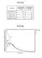
- FIG. 5A is a table showing examples of irradiation laser beams according to the embodiment.
- FIG. 5B is a graph showing numerical results of temperature distributions on a shallowest (hottest) layer in a test object according to the embodiment
- FIG. 6A is a flowchart illustrating a main process of a thermal laser stimulation method performed by the thermal laser stimulation apparatus according to the embodiment
- FIG. 6B is a flowchart for explaining step S 102 in FIG. 6A in more detail
- FIG. 6C is a flowchart for explaining steps S 112 and S 115 in FIG. 6B in more detail;
- FIG. 6D is a flowchart for explaining step S 121 in FIG. 6C in more detail
- FIG. 6E is a graph for explaining the interpolation process in step S 135 in FIG. 6D ;
- FIG. 7A is a graph for explaining the extrapolation process in step S 135 for determining a permissible power in four sets of irradiation parameters
- FIG. 7B is a graph illustrating the numerical results of the temperature on a shallowest layer when irradiating with the permissible power found in step S 135 for the four sets of the irradiation parameters;
- FIG. 8 is a diagram illustrating a precision estimate from numerical simulation for four different kinds of irradiation listed in FIG. 5A according the embodiment
- FIG. 9A is a diagram illustrating examples of three doughnut radii according to embodiment.
- FIG. 9B is a diagram illustrating a precision estimate for a doughnut irradiation for three doughnut radii shown in FIG. 9A according to embodiment
- FIG. 9C is a diagram illustrating examples of three doughnut-shaped beams with a different Gaussian-doughnut combination ratio and fixed Gaussian and doughnut radii according to the embodiment.
- FIG. 9D is a diagram illustrating a precision estimate for the five beams shown in FIG. 9C according to the embodiment.
- FIG. 10A is a schematic diagram showing an example of an optical system according to the embodiment.
- FIG. 10B is upper and side views of a schematic diagram of the test object and an irradiated zone that is generated due to an incidence of the modified laser beam onto the test object according to the embodiment;
- FIG. 10C is a lateral view schematic diagram of the test object according to the embodiment.
- FIG. 11 is a schematic diagram showing another example of the optical system according to the embodiment.
- a common test object could be, but is not limited to, a multilayer semiconductor or semiconductor device with inner circuit patterns.
- the following embodiments significantly advance conventional Optical Beam Induced Resistance Change (OBIRCH) by using a disclosed method to control a heat source, such as a doughnut-shaped heat source, in order to achieve a more efficient thermal stimulation of a test object.
- OBIRCH Optical Beam Induced Resistance Change
- Each of the embodiments relates to the method for performing an efficient thermal laser stimulation of faults embedded in a test objects that can be, but are not limited to, a multilayer semiconductor or a very-large-scale integration (VLSI) device.
- the efficient thermal stimulation achieved with one of the disclosed embodiments allows a subsequent detection, analysis, and/or identification of faults embedded in the test object by, for example, measuring a change of any thermophysical properties (e.g., electrical resistivity) or related physical value (e.g., electrical resistance) in a part or a plurality of circuits inside the test object.
- thermophysical properties e.g., electrical resistivity
- related physical value e.g., electrical resistance
- LVI Laser Voltage Imaging
- OBIRCH Optical Beam Induced Resistance Change
- a thermal laser stimulation apparatus a method of thermally stimulating, and a program, which can sufficiently stimulate faults deeply embedded in a test object, such as VLSI, while decreasing the temperature inside the test object in order to keeping it below a permissible temperature, will be explained. According to the embodiments, it becomes possible to perform a nondestructive failure analysis of a test object with deeply embedded faults.
- FIG. 1 illustrates a concept of a thermal laser stimulation according to an embodiment.
- an optical system 3 is used for modifying a laser beam C 0 outputted from a laser source 2 , which may have a Gaussian intensity profile, into a modified laser beam C 3 whose wavefront is characteristic of generating two or more intensity components: one intensity component C 1 that increases the intensity near the irradiation axis 4 ; and another intensity component C 2 that increases the intensity around the irradiation axis 4 .
- the intensity component C 1 may have a Gaussian intensity profile of which peak intensity is weaker than that of the laser beam C 0
- the intensity component C 2 may have a doughnut-shape intensity profile of which peak intensity is around the intensity component C 1 .
- FIG. 2 is a diagram illustrating a configuration of a thermal laser stimulation apparatus according to the embodiment.
- the thermal laser stimulation apparatus 100 comprises a computer system 101 , a display 102 , a signal generator 103 , an environment control system 104 , a signal detector 105 , a laser source 2 , and an optical system 3 .
- the laser source 2 outputs a laser beam C 0 .
- the optical system 3 modifies the intensity pattern of the laser beam C 0 according to the following method, and directs the modified laser beam C 3 with the two intensity components C 1 and C 2 onto a test object 1 .
- the optical system 3 also scans the laser beam C 3 on one or more surfaces of the test object 1 .
- the environment control system 104 controls the ambient temperature, humidity, and pressure inside the thermal laser stimulation apparatus 100 .
- the environment control system 104 also control the initial temperature and boundary temperature of a test object 1 .
- the computer system 101 controls the thermal laser apparatus 100 , determines a set of thermal laser stimulation conditions, and performs a failure analysis from the output signal of the signal detector 105 .
- the signal generator 103 generates a signal inside one or more preselected circuits in a test object 1 .
- the signal detector 105 measures the generated (unstimulated) signal and/or stimulated signal in one or more preconditioned circuits as the heat source is scanned on the test object 1 .
- the signal detector 105 also outputs the measured data to the computer system 101 .
- the display 102 outputs the conditions and results of the failure analysis performed by the computer system 101 .
- the modified laser beam C 3 can consist on any pattern characteristic of having the intensity component (hereinafter referred to as central component) C 1 near the irradiation axis 4 and the intensity component (hereinafter referred to as peripheral component) C 2 surrounding the central component C 1 .
- Central axes of the two intensity components C 1 and C 2 have the same location as the irradiation axis 4 or in its proximity.
- FIG. 3A shows a modified laser beam C 13 according to a first example.
- This simple modified laser beam C 13 comprises a spot-like component C 11 and a ring-like component C 12 .
- the spot-like component C 11 corresponds to the central component C 1
- the ring-like component C 12 corresponds to the peripheral component C 2 .
- the spot-like component C 11 is surrounded by the ring-like component C 12 .
- the spot-like component C 11 and the ring-like component C 12 are considered as a Gaussian intensity profile and a doughnut-shaped intensity profile, respectively.
- FIG. 3B shows another modified laser beam C 23 according to a second example.
- the modified laser beam C 23 comprises a spot-like component C 21 corresponding to the central component C 1 and multiple concentric ring components C 22 corresponding to the peripheral component C 2 .
- the spot-like component C 21 is surrounded by the multiple concentric ring components C 22 .
- These multiple concentric ring components C 22 could be formed by superimposing multiple doughnut-shaped intensities.
- the modified laser beam C 23 could be formed by focusing a laser beam near its theoretical limit where a Gaussian-like profile is surrounded by multiple local maximums, such as in an Airy disk.
- FIG. 3C shows yet another modified laser beam C 33 according to a third example.
- the modified laser beam C 33 comprises a central Gaussian component C 31 corresponding to the central component C 1 and peripheral Gaussian components C 32 corresponding to the peripheral component C 2 .
- the central Gaussian component C 31 is surrounded by the peripheral Gaussian components C 32 whose centroid (or weighted arithmetic mean) coincides with that of the central Gaussian component C 31 .
- four Gaussian components C 32 form the peripheral component C 2 ; however the peripheral component C 2 could be formed by two or more Gaussian components C 32 .
- Characteristics of the modified laser beam C 3 can be controlled using the following irradiation parameters, for instance.
- the irradiation parameters may include: a laser power P G of Gaussian distribution (C 1 ), a laser power P D of a doughnut-shaped distribution (C 2 ), a characteristic radius w G of the Gaussian distribution (C 1 ), and a characteristic radius w D of the doughnut-shaped distribution (C 2 ).
- Equation (1) The irradiation parameters are introduced into Equation (1).
- an irradiation of the test object 1 with the modified laser beam C 3 generates a three-dimensional heat generation profile S in the test object 1 as described by Equation (1).
- This heat generation profile could also be a numerical result of an optical calculation or an approximation function alternative to Equation (1).
- Equation (1) x, y and z are Cartesian coordinates ( ⁇ y is a direction of a depth; x and z are on a two-dimensional plane of a chip) and ⁇ is the attenuation coefficient defined in Equation (2).
- Equation (2) K is an extinction coefficient and ⁇ 0 is a wavelength.
- the irradiation of the test object 1 with the modified laser beam C 3 that generates the three-dimensional heat generation profile S according to Equation (1) would reduce the maximum temperature inside the test object 1 in comparison to a single (conventional) Gaussian irradiation.
- FIG. 4 shows heat generation profiles in cases that the test object 1 is irradiated with a laser beam with a Gaussian intensity profile (hereinafter referred to as a Gaussian laser beam), a laser beam with a doughnut-shape intensity profile (hereinafter referred to as a doughnut-shape laser beam), and the modified laser beam according to the embodiment, respectively.
- a line G 1 shows a heat generation profile in a first case where the test object 1 is irradiated with the Gaussian laser beam
- a line D 1 shows a heat generation profile in a second case where the test object 1 is irradiated with the doughnut-shape laser beam
- a line M 1 shows a heat generation profile in a third case where the test object 1 is irradiated with the modified laser beam C 3 .
- generated heat is distributed from an irradiation axis to its peripheral area thereof.
- a first variation (GAUSSIAN) is a Gaussian laser beam of which a Gaussian component P G is 100 [u] and a doughnut component P D is 0 [u].
- a second variation (CASE A) is a modified laser beam (one variation of the modified laser beam C 3 ) of which the Gaussian component P G is 15 [u] and the doughnut component P D is 85 [u].
- a third variation is a modified laser beam (another variation of the modified laser beam C 3 ) of which the Gaussian component P G is 10 [u] and the doughnut component P D is 90 [u].
- a fourth variation is a doughnut-shape laser beam of which a Gaussian component P G is 0 [u] and a doughnut component P D is 100 [u].
- a line G 2 shows a maximum temperature when the test object 1 is irradiated with the first variation laser beam
- a line M 2 shows a maximum temperature when the test object 1 is irradiated with the second variation laser beam
- a line M 3 shows a maximum temperature when the test object 1 is irradiated with the third variation laser beam
- a line D 2 shows a maximum temperature when the test object 1 is irradiated with the fourth variation laser beam.
- FIG. 5B shows advantageous effects where the maximum temperatures on the surface of the test object 1 are considerably reduced for the second to fourth variation laser beams in comparison to the first variation laser beam. Moreover, for this net power, the maximum temperature for the first variation laser beam surpasses the permissible temperature (T>T perm ). In contrast, for the second to fourth variation laser beams, i.e., for the irradiation laser beam including the doughnut component, the maximum temperature is below the permissible temperature (T ⁇ T perm ); hence, a cooler surface is reached when a doughnut component is applied. As stated above, a decrease of maximum temperature allows a further increase of the laser power, which leads to an enhanced thermal laser stimulation that improves the accuracy in a failure analysis test.
- FIGS. 6A to 6D are flowcharts of a thermal laser stimulation method according to the embodiment.
- FIG. 6A shows a flowchart illustrating a main process of the thermal laser stimulation method performed by the thermal laser stimulation apparatus according to the embodiment.
- the computer system 101 estimates a depth X of a fault by an electrical method before thermally stimulating the test object 1 .
- a constant voltage can be applied to each of the layers with the signal generator 103 and, when one fault or multiple faults are located on a given layer, then the current measured with the signal detector 105 would significantly differ from those layers that lack faults, i.e., for a faulty layer there is an anomaly in the current measurement.
- the signal detector 105 can detect anomalies of the voltage.
- the depth of the fault X (target depth) can be estimated based on a layer number and a blueprint of the structure of the test object 1 , e.g., providing information on layer thickness.
- the computer system 101 improves the irradiation parameters T ( ⁇ , w G , w D ) in order to enhance the thermal stimulation of a fault.
- the computer system 101 sets the improved parameters in the laser source 2 , the optical system 3 and the environment control system 104 of the thermal stimulation apparatus 100 .
- the computer system 101 analyzes a set of stimulated signals detected by the signal detector 105 .
- Step S 102 in FIG. 6A is explained in more detail in a flowchart illustrated in FIG. 6B .
- the step S 102 is an irradiation parameter improvement that results in an enhancement (or optimization) of the thermal laser stimulation method according to the embodiment.
- the computer system 101 introduces an initial set of irradiation parameters. These initial set of irradiation parameters can be set arbitrarily within the technical boundaries of the laser source 2 and the optical system 3 .
- step S 112 the computer system 101 obtains a precision estimate ⁇ 0 for the initial set of irradiation parameters.
- step S 113 the computer system 101 determines whether the precision estimate ⁇ 0 for the initial set of irradiation parameters is good enough, i.e., whether the precision estimate ⁇ 0 is less than an objective precision ⁇ obj .
- the objective precision ⁇ obj usually depends on the resolution of a final destructive method that is used to analyze the fault after a noninvasive detection method, such as the disclosed thermal stimulation apparatus.
- the computer system 101 finishes this operation because the initial estimate ⁇ 0 is good enough for detecting the fault in the test object.
- step S 114 the computer system 101 introduces a new set of irradiation parameters. If step S 114 is executed for the first time, then this new set of parameters is chosen arbitrarily within the technical boundaries of the laser source 2 and the optical system 3 , but different from the initial set of irradiation parameters. If step S 114 is not executed for the first time, then the new set of parameters ( ⁇ 1 , w G 1 , w D 1 ) will be determined based on a method executed in step S 118 . After executing step S 114 , the computer system 101 obtains a new precision estimate ⁇ 1 by executing the step S 115 .
- step S 116 the computer system 101 obtains a difference a between the initial precision estimate 0° and the new precision estimate ⁇ 1 .
- step S 117 the computer system 101 checks one or two conditions; first, whether ⁇ 1 is less than ⁇ 0 ; second, whether the difference ⁇ is smaller than a given value ⁇ min . When one or both of these conditions is met (step S 117 ; YES), then the computer system 101 finishes this operation because the precision estimate (is good enough or it cannot be further improved.
- ⁇ 0 corresponds to the initial precision estimate output from step S 112
- the second time the step S 116 is executed ⁇ 0 corresponds to the previous value of ⁇ 1 as determined in step S 119 .
- step S 118 where various gradients (and/or Jacobians) are determined because any available method can be readily used, e.g., Conjugate Gradient Method (CGM) or Steepest Descent Method (SDM) or Genetic Algorithms (GA).
- CGM Conjugate Gradient Method
- SDM Steepest Descent Method
- GA Genetic Algorithms
- Steps S 112 and S 115 in FIG. 6B are explained in more detail in a flowchart illustrated in FIG. 6C .
- the steps S 112 and S 115 are precision estimate processes of a thermal laser stimulation method according to the embodiment.
- the computer system 101 determines a permissible laser power P perm .
- the computer system 101 determines the temperature field T for the permissible laser power.
- the computer system 101 determines a maximum temperature T max at the target depth X, and then the computer system 101 estimates a signal (which is detectable with the signal detector 105 ) from the maximum temperature T max and noises ⁇ .
- step S 124 the computer system 101 obtains a precision estimate for the corresponding irradiation parameters and its permissible laser power P perm .
- Step S 121 in FIG. 6C is explained in more detail in a flowchart illustrated in FIG. 6D .
- the step S 121 is a permissible temperature estimate process for a thermal laser stimulation method according to the embodiment.
- the computer system 101 decides two laser power values P 1 and P 2 within the technical constraints of the laser source 2 .
- step S 132 the computer system 101 determines the heat source S 1 ( ⁇ , w G , w D ) and S 2 ( ⁇ , w G , w D ) for the laser powers P 1 and P 2 , respectively.
- the heat source S has the form described in Equation (1) according to the embodiment.
- a heat source S can have a plurality of shapes as those shown in FIGS. 3A to 3C , and the heat source S can be estimated with a plurality of methods or a combination of such.
- a computational electromagnetics method that solves light phenomena, e.g., scattering and diffraction in periodic dielectric structures, could be used to estimate a heat source S that directly results from light absorption in the test object.
- step S 133 the computer system 101 determines temperature fields T 1 and T 2 for the laser powers P 1 and P 2 , respectively.
- the temperature fields T 1 and T 2 can be determined by a diversity of methods. According to the embodiment, T is determined by a numerical calculation that is based on a heat diffusion equation where the temperature T is governed by the following Equation (3).
- Equation (3) ⁇ x , ⁇ y , and ⁇ z are the thermal conductivities in a system of Cartesian coordinates, ⁇ is density, c p is the specific heat capacity, and t is time. Equation (3) is corresponded to the governing equation of T in an infinitesimal control volume dx ⁇ dy ⁇ dz.
- thermophysical properties ⁇ x , ⁇ y , ⁇ z (different to ⁇ 0 that is the wavelength), ⁇ and c p are local properties within the infinitesimal volume.
- bulk thermophysical properties could be determined, e.g., using thermal resistance circuits, in order to ease a numerical calculation.
- the same principle applies to the attenuation coefficient ⁇ in Equation (2).
- Equation (3) is used in the embodiment, a plurality of methods could be used to determine the temperature field. For example, a statistical analysis based on a Monte Carlo Method and/or Boltzmann transport equations could be sought for predicting phonon dispersion and estimating a temperature field T inside the test object.
- step S 134 the computer system 101 determines maximum temperatures T max1 and T max2 for the temperatures fields T 1 and T 2 , respectively.
- step S 135 as shown in FIG. 6E , using the laser powers P 1 and P 2 and the maximum temperatures T max1 and T max2 , the computer system 101 determines by extrapolation (or interpolation) the permissible laser power P perm , i.e., the maximum power where there is no damage in the test object 1 .
- FIGS. 7A and 7B show the extrapolation process in step S 135 and the numerical results with a permissible power for four sets of irradiation parameters.
- a line G 11 shows a relationship for the Gaussian laser beam
- a line D 11 shows a relationship for the doughnut laser beam
- lines M 11 and M 12 show relationships for the two modified laser beams of the CASEs A and B, respectively.
- the CASEs A and B consist of a doughnut components of 85% and 90%, respectively, of the total irradiation power P (see table in FIG. 5A ).
- the maximum temperature in FIG. 7A is normalized with the permissible temperature T perm , so that T max ⁇ 1 means that the maximum temperature inside the test object 1 is less than the permissible temperature.
- T max ⁇ 1 means that the maximum temperature inside the test object 1 is less than the permissible temperature.
- T max ⁇ 1 means that the maximum temperature inside the test object 1 is less than the permissible temperature.
- T max ⁇ 1 means that the maximum temperature inside the test object 1 is less than the permissible temperature.
- the relationship between irradiation power P and maximum temperature T max is linear. Therefore, an extrapolation (or interpolation) can be made to estimate the permissible laser power P p e ⁇ r as shown in FIG. 7A .
- FIG. 7B shows the numerical results of the temperature on the shallowest layer for the extrapolated permissible power for four sets of irradiation parameters.
- FIG. 8 shows that, in fact, a better measurement precision (is achieved in deep layers when the test object 1 is irradiated with the modified laser beam C 3 with the peripheral component C 2 .
- the abscissa axis is the depth while the ordinate axis is a dimensionless precision estimate ⁇ , where ⁇ is normalized with a permissible precision ⁇ perm .
- a line G 31 shows a relationship between a measurement precision ⁇ and a depth for the Gaussian laser beam
- a line D 31 shows a relationship between a measurement precision ⁇ and a depth for the doughnut laser beam
- lines M 31 and M 32 show relationships between measurement precisions ⁇ and depths for the two modified laser beams of the CASEs A and B, respectively.
- FIG. 8 shows that in shallow layers the doughnut-shape laser beam could worsen the measurement precision. Such deterioration is expected since the doughnut-shape laser beam has a region that is more broadly thermally stimulated in shallow layers than its Gaussian counterpart, as suggested by the intensity profile shown in FIG. 4 .
- a doughnut-shaped laser beam with an increased characteristic radius w D enhances the measurement precision for faults in deep layers of the test object 1 , as shown in FIGS. 9A and 9B .
- a plurality of optical apparatus and methods are presented for generating a tunable combination of Gaussian and doughnut-shaped irradiation according to the embodiment.
- FIG. 10A shows an arrangement of the optical system 3 in the thermal laser stimulation apparatus 100 according to the embodiment.
- the optical system 3 is used to manipulate laser beams outputted from the laser sources 2 including laser sources 2 G and 2 D.
- the optical system 3 comprises ND filters 11 G and 11 D, polarizing plates 12 G and 12 D, a wavefront converter 13 , beam expanders 40 G and 40 D, a beam splitter 51 , a camera 41 , a beam collector 52 , an optical element 53 , a scanner 54 , a lens 10 , a circuit board 30 , a stage 50 , and a stand 80 .
- the computer system 101 shown in FIG. 2 is used to control several elements in the optical system 3 and to record the electric signal changes measured from the test object 1 using the signal detector 105 .
- laser sources 2 G and 2 D output laser beams C 10 and C 20 , respectively, with an independent Gaussian intensity profile.
- the intensity of the laser beams C 10 and C 20 can be adjusted with ND filters 11 G and 11 D, respectively.
- Laser beams C 10 and C 20 can also respectively pass through polarizing plate 12 G and 12 D in order to guarantee a desired linear polarization state, e.g., 45 degree angle respect to a horizontal reference line; if the linear polarization state of laser beams C 10 and C 20 is known just after exiting the laser source 2 G and 2 D, respectively, then polarizing plates 12 G and/or 12 D could be omitted.
- the beam expander 40 G comprises a concave lens 41 G, a convex lens 42 G and an actuator 43 G.
- the laser beam C 10 is expanded by the concave lens 40 G, and then, the expanded laser beam C 10 is collimated by the convex lens 42 G.
- the actuator 43 G adjusts the position of convex lens 42 G, whose focus can also be changed in order to control the radius w G of the Gaussian intensity profile of laser beam C 10 . After which, the laser beam C 10 enters the beam splitter 51 .
- the laser source 2 D outputs a laser beam C 20 whose intensity is modified to a doughnut-shape intensity profile by the wavefront converter 13 .
- the beam expander 40 D comprises a concave lens 41 D, a convex lens 42 D and an actuator 43 D.
- the laser beam C 20 is expanded by the concave lens 41 D, and then, the expanded laser beam C 20 is collimated by the convex lens 42 D.
- the actuator 43 D adjusts the position of convex lens 42 D, whose focus can also be changed in order to control the radius w D of the doughnut-shaped intensity profile of laser beam C 20 . After which, the laser beam C 20 enters the beam splitter 51 .
- the beam splitter 51 may be a polarizer or any kind of mirror and/or prism.
- the beam splitter 51 generates the modified laser beam C 3 by multiplexing the laser beams C 10 and C 20 , and emits the modified laser beam C 3 toward the test object 1 .
- the beam splitter 51 may also emit the intensity profile of beams C 10 and C 20 to the camera 41 in order manage the adjustment of the laser beam intensities, e.g., I D and I G that comprise P G and P D and radii w G and w D in Equation (1).
- the beam splitter 51 can also be removed in order to adjust the laser beam C 10 , or the beam splitter 51 can be changed with a fixed mirror in order to adjust the laser beam C 20 .
- the modified laser beam C 3 emitted from the beam splitter 51 is focused on the test object 1 by passing through the beam collector 52 .
- the beam collector 52 can be any one of, or a combination of, one or more concave lenses and/or one or more convex lenses and/or one or more objective lenses.
- the modified laser beam C 3 then passes through the optical element 53 that is used to scan an irradiated zone on the test object 1 .
- the optical element 53 can be a flat plate, a mirror, a lens, or any other element that can be used for scanning the laser beam C 3 .
- the optical element 53 is manipulated with the scanner 54 that can comprise a Piezo element and/or a servo motor and/or a stepper motor and/or a linear motor.
- the modified laser beam C 3 is then focused on the test object 1 via the lens 10 .
- the lens 10 can be a solid immersed lens (SIL) or any derivative in order to modify the numerical aperture of the optical system 3 .
- Equation (4) ⁇ is the diameter of the irradiated zone created by the incidence of the modified laser beam C 3 on the shallow layers of the test object 1 , ⁇ is a wavelength of the modified laser beam C 3 , and NA is the numerical aperture of the optical system 3 .
- Equation (4) is formulated according to an ideal Airy disk intensity distribution on the shallow layers.
- the wavelength of the modified laser beam C 3 is usually in the infrared region to reduce the absorption in a substrate 25 of the test object 1 (see FIG. 10C ).
- a NA and A in the optical system 3 should be selected according to a value that maximizes the accuracy of the measurement, e.g., following the process described in FIG. 6A .
- the test object 1 is mounted on the circuit board 30 wherein different pins of peripherals of the test object 1 are wired to the circuit board 30 .
- the circuit board 30 is used to apply a constant or variable voltage difference along one path in the test object 1 or multiple paths in the test object 1 , wherein these paths may include individual layers of the test object 1 in order to detect a depth of each failure.
- the circuit board 30 is fixed on the stage 50 .
- the stage 50 is used to control a spatial location of the test object 1 in the optical system 3 ; the spatial location can be controlled in any of three Cartesian coordinates.
- the stage 50 is mounted on the stand 80 , which can comprise damping features in order to isolate the optical system 3 from external vibrations that can potentially affect measurement accuracy.
- FIG. 10B shows upper and side views of a schematic diagram of a typical multilayer flash memory chip as the test object 1 and an irradiated zone Z 10 that is generated due to the incidence of the modified laser beam C 3 onto a multilayer zone 26 of the test object 1 .
- a typical multilayer flash memory structure is used as a general example of the test object 1 ; however, any planar or multilayer semiconductor device can be analyzed with the presented embodiments.
- the object does not need to have a periodic structure neither a pre-established structural characteristic.
- FIG. 10C shows a lateral view schematic diagram of the test object 1 .
- An intensity of the irradiated zone Z 10 on a shallow layers 26 a of the test object 1 is also shown in FIG. 10C , which corresponds to the lateral view of the test object 1 shown in FIG. 10B .
- the embodiment is primarily directed to detect faults in the deep layers 26 b , but it can also detect faults in the shallow layers 26 a . Since infrared irradiation is highly absorbed by different materials in the circuit layers 27 , then the laser beam C 3 is preferably directed through the substrate layer 25 , which is usually made of one material semi-transparent against the wavelength ⁇ of the modified laser beam C 3 .
- FIG. 11 shows another arrangement of the optical system 3 in the thermal laser stimulation apparatus 100 according to the embodiment.
- the same reference numbers will be applied, and the redundant explanations thereof will be omitted.
- the optical system 300 is used to manipulate a laser beam outputted from the laser source 2 .
- the optical system 300 comprises an ND filter 11 , a polarizing plate 12 , a beam expander 40 , a beam splitter 55 , an adjustable mirror 60 G, an actuator 61 , a wavefront converter 13 , a fixed mirror 60 D, the beam splitter 51 , the camera 41 , the beam collector 52 , a fixed mirror 62 , an adjustable mirror 63 , a scanner 64 , the lens 10 , the circuit board 30 , the stage 50 , and the stand 80 .
- the laser source 2 outputs a laser beam C 30 with a Gaussian intensity profile.
- the laser beam C 30 could pass through the ND filter 11 and polarizing plate 12 in order to control the intensity and linear polarization of the laser beam C 30 , respectively; if the intensity or linear polarization state of the laser beam C 30 is known just after exiting the laser source 2 , then optical elements 11 and 12 could be omitted.
- a direction of the desired linear polarization state is slanted by ⁇ ( ⁇ is 45°, for instance) with respect to the horizontal direction.
- the beam expander 40 comprises a concave lens 41 and a convex lens 42 , and expands a diameter of the laser beam C 30 .
- the expanded laser beam C 30 is split into two laser beams.
- One laser beam is the Gaussian laser beam C 1 , and it is introduced to the beam splitter 51 through a reflection by the adjustable mirror 60 G.
- the other laser beam is converted into the doughnut-shape laser beam (corresponding to the peripheral component C 2 ) by passing through the wavefront converter 13 .
- the wavefront converter 13 may comprise axicon mirrors/lenses, and converts a Gaussian laser beam into a doughnut-shape laser beam.
- the doughnut-shape laser beam (C 2 ) outputted from the wavefront converter 13 enters the beam splitter 51 through reflection by the fixed mirror 60 D.
- the beam splitter 51 generates the modified laser beam C 3 by multiplexing the laser beams (C 1 and C 2 ), and emits the modified laser beam C 3 toward the test object 1 .
- the modified laser beam C 3 emitted from the beam splitter 51 is focused on the test object 1 by passing through the beam collector 52 .
- the modified laser beam C 3 is reflected by the fixed mirror 62 , and then passes through the adjustable mirror 63 that is used to scan an irradiated zone on the test object 1 .
- the adjustable mirror 63 is manipulated with the scanner 64 that can comprise a Piezo element and/or a servo motor and/or a stepper motor and/or a linear motor. Then, the modified laser beam C 3 is focused on the test object 1 via the lens 10 .
Landscapes
- Engineering & Computer Science (AREA)
- Physics & Mathematics (AREA)
- Electromagnetism (AREA)
- Microelectronics & Electronic Packaging (AREA)
- General Physics & Mathematics (AREA)
- Health & Medical Sciences (AREA)
- General Engineering & Computer Science (AREA)
- Toxicology (AREA)
- Computer Hardware Design (AREA)
- Plasma & Fusion (AREA)
- Environmental & Geological Engineering (AREA)
- Optics & Photonics (AREA)
- Computer Vision & Pattern Recognition (AREA)
- Investigating Or Analyzing Materials Using Thermal Means (AREA)
- Testing Or Measuring Of Semiconductors Or The Like (AREA)
Applications Claiming Priority (2)
| Application Number | Priority Date | Filing Date | Title |
|---|---|---|---|
| JP2016-053114 | 2016-03-16 | ||
| JP2016053114A JP6441252B2 (ja) | 2016-03-16 | 2016-03-16 | 熱レーザ刺激装置、熱レーザ刺激方法および記録媒体 |
Publications (2)
| Publication Number | Publication Date |
|---|---|
| US20170269154A1 US20170269154A1 (en) | 2017-09-21 |
| US10359468B2 true US10359468B2 (en) | 2019-07-23 |
Family
ID=59855671
Family Applications (1)
| Application Number | Title | Priority Date | Filing Date |
|---|---|---|---|
| US15/389,917 Active 2037-10-18 US10359468B2 (en) | 2016-03-16 | 2016-12-23 | Thermal laser stimulation apparatus, method of thermally stimulating, and non-transitory computer readable medium |
Country Status (2)
| Country | Link |
|---|---|
| US (1) | US10359468B2 (ja) |
| JP (1) | JP6441252B2 (ja) |
Families Citing this family (1)
| Publication number | Priority date | Publication date | Assignee | Title |
|---|---|---|---|---|
| JP2021121785A (ja) * | 2020-01-31 | 2021-08-26 | 浜松ホトニクス株式会社 | 半導体故障解析装置 |
Citations (17)
| Publication number | Priority date | Publication date | Assignee | Title |
|---|---|---|---|---|
| US5103073A (en) * | 1987-08-28 | 1992-04-07 | Danilov Viktor A | Device for laser treatment of an object |
| JPH09260286A (ja) | 1996-03-27 | 1997-10-03 | Sharp Corp | 半導体装置の製造方法 |
| JPH1050784A (ja) | 1996-08-07 | 1998-02-20 | Nec Corp | 半導体デバイスの寄生MIM構造箇所解析法及びSi半導体デバイスの寄生MIM構造箇所解析法 |
| JP2005045144A (ja) | 2003-07-25 | 2005-02-17 | Matsushita Electric Ind Co Ltd | 検査装置および検査方法 |
| JP2005300250A (ja) | 2004-04-08 | 2005-10-27 | Canon Inc | 光干渉測定装置、光干渉測定方法、光学素子、及び露光装置 |
| US20070096763A1 (en) * | 2005-10-18 | 2007-05-03 | Gsi Group Corporation | Methods and apparatus for utilizing an optical reference |
| US20070115003A1 (en) * | 2005-11-02 | 2007-05-24 | Nec Electronics Corporation | Non-destructive testing apparatus and non-destructive testing method |
| JP2010197051A (ja) | 2009-02-20 | 2010-09-09 | Toshiba Corp | 故障解析装置 |
| JP2012138456A (ja) | 2010-12-27 | 2012-07-19 | Fujitsu Ltd | 配線構造、半導体装置及び不良箇所特定方法 |
| JP2012222263A (ja) | 2011-04-13 | 2012-11-12 | Renesas Electronics Corp | 半導体装置の不良解析方法、チップ状半導体装置の不良解析方法及び半導体装置の動的不良解析装置 |
| JP2013036953A (ja) | 2011-08-11 | 2013-02-21 | Fujitsu Ltd | 半導体装置及び検査方法 |
| JP2013104667A (ja) | 2011-11-10 | 2013-05-30 | Fujitsu Semiconductor Ltd | 半導体装置の検査装置及び検査方法 |
| JP2014107483A (ja) | 2012-11-29 | 2014-06-09 | Fujitsu Semiconductor Ltd | Obirch検査方法及びobirch装置 |
| JP2014143348A (ja) | 2013-01-25 | 2014-08-07 | Renesas Electronics Corp | 半導体装置の不良解析方法、および不良解析装置 |
| JP2014175421A (ja) | 2013-03-07 | 2014-09-22 | Japan Steel Works Ltd:The | ゲッタリング半導体ウエハおよびその製造方法 |
| JP2015032686A (ja) | 2013-08-02 | 2015-02-16 | 信越半導体株式会社 | 半導体素子の評価方法及び半導体素子の評価装置 |
| US20170074928A1 (en) | 2015-09-16 | 2017-03-16 | Kabushiki Kaisha Toshiba | Apparatus and method for detecting faults in multilayer semiconductors |
Family Cites Families (7)
| Publication number | Priority date | Publication date | Assignee | Title |
|---|---|---|---|---|
| JP3698904B2 (ja) * | 1999-01-11 | 2005-09-21 | 沖電気工業株式会社 | 半導体評価方法及び欠陥位置特定装置 |
| JP2001074817A (ja) * | 1999-07-06 | 2001-03-23 | Jeol Ltd | 半導体デバイス評価方法及び装置 |
| KR100524213B1 (ko) * | 2003-02-28 | 2005-10-27 | 삼성전자주식회사 | 기판 검사 방법 및 장치 |
| JP4897334B2 (ja) * | 2006-03-31 | 2012-03-14 | 株式会社トプコン | 表面検査方法及び表面検査装置 |
| FR2919402B1 (fr) * | 2007-07-23 | 2009-10-30 | Eads Europ Aeronautic Defence | Procede de test d'une application logicielle. |
| JP5929293B2 (ja) * | 2012-02-20 | 2016-06-01 | 株式会社Screenホールディングス | 検査装置および検査方法 |
| JP6317321B2 (ja) * | 2013-02-19 | 2018-04-25 | 浜松ホトニクス株式会社 | 電界集中位置観察装置および電界集中位置観察方法 |
-
2016
- 2016-03-16 JP JP2016053114A patent/JP6441252B2/ja active Active
- 2016-12-23 US US15/389,917 patent/US10359468B2/en active Active
Patent Citations (20)
| Publication number | Priority date | Publication date | Assignee | Title |
|---|---|---|---|---|
| US5103073A (en) * | 1987-08-28 | 1992-04-07 | Danilov Viktor A | Device for laser treatment of an object |
| JPH09260286A (ja) | 1996-03-27 | 1997-10-03 | Sharp Corp | 半導体装置の製造方法 |
| JPH1050784A (ja) | 1996-08-07 | 1998-02-20 | Nec Corp | 半導体デバイスの寄生MIM構造箇所解析法及びSi半導体デバイスの寄生MIM構造箇所解析法 |
| US6320396B1 (en) | 1996-08-07 | 2001-11-20 | Nec Corporation | Parasitic MIM structural spot analysis method for semiconductor device and parasitic MIM structure spot analysis method for silicon semiconductor device |
| JP2005045144A (ja) | 2003-07-25 | 2005-02-17 | Matsushita Electric Ind Co Ltd | 検査装置および検査方法 |
| JP2005300250A (ja) | 2004-04-08 | 2005-10-27 | Canon Inc | 光干渉測定装置、光干渉測定方法、光学素子、及び露光装置 |
| US20070096763A1 (en) * | 2005-10-18 | 2007-05-03 | Gsi Group Corporation | Methods and apparatus for utilizing an optical reference |
| US20070115003A1 (en) * | 2005-11-02 | 2007-05-24 | Nec Electronics Corporation | Non-destructive testing apparatus and non-destructive testing method |
| JP2007127499A (ja) | 2005-11-02 | 2007-05-24 | Nec Electronics Corp | 非破壊検査装置および非破壊検査方法 |
| JP2010197051A (ja) | 2009-02-20 | 2010-09-09 | Toshiba Corp | 故障解析装置 |
| JP2012138456A (ja) | 2010-12-27 | 2012-07-19 | Fujitsu Ltd | 配線構造、半導体装置及び不良箇所特定方法 |
| JP2012222263A (ja) | 2011-04-13 | 2012-11-12 | Renesas Electronics Corp | 半導体装置の不良解析方法、チップ状半導体装置の不良解析方法及び半導体装置の動的不良解析装置 |
| JP2013036953A (ja) | 2011-08-11 | 2013-02-21 | Fujitsu Ltd | 半導体装置及び検査方法 |
| JP2013104667A (ja) | 2011-11-10 | 2013-05-30 | Fujitsu Semiconductor Ltd | 半導体装置の検査装置及び検査方法 |
| JP2014107483A (ja) | 2012-11-29 | 2014-06-09 | Fujitsu Semiconductor Ltd | Obirch検査方法及びobirch装置 |
| JP2014143348A (ja) | 2013-01-25 | 2014-08-07 | Renesas Electronics Corp | 半導体装置の不良解析方法、および不良解析装置 |
| JP2014175421A (ja) | 2013-03-07 | 2014-09-22 | Japan Steel Works Ltd:The | ゲッタリング半導体ウエハおよびその製造方法 |
| JP2015032686A (ja) | 2013-08-02 | 2015-02-16 | 信越半導体株式会社 | 半導体素子の評価方法及び半導体素子の評価装置 |
| US20170074928A1 (en) | 2015-09-16 | 2017-03-16 | Kabushiki Kaisha Toshiba | Apparatus and method for detecting faults in multilayer semiconductors |
| JP2017058225A (ja) | 2015-09-16 | 2017-03-23 | 株式会社東芝 | 欠陥検出装置、欠陥検出方法およびプログラム |
Also Published As
| Publication number | Publication date |
|---|---|
| JP2017167006A (ja) | 2017-09-21 |
| US20170269154A1 (en) | 2017-09-21 |
| JP6441252B2 (ja) | 2018-12-19 |
Similar Documents
| Publication | Publication Date | Title |
|---|---|---|
| US6489801B1 (en) | Apparatus and method for evaluating a semiconductor wafer | |
| JP6552513B2 (ja) | 明視野検査、暗視野検査、光熱検査を組み合わせた装置及び方法 | |
| CN105612601B (zh) | 用于图案化晶片表征的方法与设备 | |
| KR102056494B1 (ko) | 온도 성능이 개선된 2빔 레이저 어닐링 방법 및 시스템 | |
| US7705974B2 (en) | Metrology system with spectroscopic ellipsometer and photoacoustic measurements | |
| JP3654630B2 (ja) | 半導体製造での微細構造表面の製造プロセスを光学的にコントロールする方法および装置 | |
| US6812717B2 (en) | Use of a coefficient of a power curve to evaluate a semiconductor wafer | |
| US20180348055A1 (en) | Deconvolution to reduce the effective spot size of a spectroscopic optical metrology device | |
| KR20150088206A (ko) | 반도체 칩 표면검사 장치 및 이를 이용한 반도체 칩의 표면검사 방법 | |
| JP2016504569A (ja) | 最適化されたシステムパラメータによる光学計測のための装置および方法 | |
| TW201840957A (zh) | 用於小角度x射線散射量測之x射線變焦鏡頭 | |
| Yang et al. | Multi-spot laser lock-in thermography for real-time imaging of cracks in semiconductor chips during a manufacturing process | |
| TW202132771A (zh) | 基於軟性x射線散射測量之覆蓋測量方法及系統 | |
| KR101368930B1 (ko) | 시뮬레이트 회절 신호 입력을 가진 서포트 벡터 머신을 이용하는 광학 계측 방법 | |
| JP5239346B2 (ja) | ラマン分光を用いた応力評価方法及び半導体装置の製造方法 | |
| US10359468B2 (en) | Thermal laser stimulation apparatus, method of thermally stimulating, and non-transitory computer readable medium | |
| JP2008537781A5 (ja) | ||
| JP2008537781A (ja) | デュアル光音響および抵抗測定システム | |
| US10088522B2 (en) | Apparatus and method for detecting faults in multilayer semiconductors | |
| TW202340709A (zh) | 用於半導體結構之資料驅動參數化及量測之方法及系統 | |
| JP2006337037A (ja) | 故障箇所特定方法および装置 | |
| US20240004311A1 (en) | A system and method for performing alignment and overlay measurement through an opaque layer | |
| US20170131084A1 (en) | Metrology system and measurement method using the same | |
| Goloborodko et al. | Determination of surface defects by using the wavefront scanner | |
| TW202410232A (zh) | 散射熔化偵測系統及其使用方法 |
Legal Events
| Date | Code | Title | Description |
|---|---|---|---|
| AS | Assignment |
Owner name: KABUSHIKI KAISHA TOSHIBA, JAPAN Free format text: ASSIGNMENT OF ASSIGNORS INTEREST;ASSIGNORS:TORRES, JUAN FELIPE;KANO, HIROYA;SHIRATSUCHI, MASATAKA;AND OTHERS;SIGNING DATES FROM 20161209 TO 20161219;REEL/FRAME:041210/0262 |
|
| AS | Assignment |
Owner name: TOSHIBA MEMORY CORPORATION, JAPAN Free format text: ASSIGNMENT OF ASSIGNORS INTEREST;ASSIGNOR:KABUSHIKI KAISHA TOSHIBA;REEL/FRAME:043088/0620 Effective date: 20170612 |
|
| STPP | Information on status: patent application and granting procedure in general |
Free format text: RESPONSE TO NON-FINAL OFFICE ACTION ENTERED AND FORWARDED TO EXAMINER |
|
| STPP | Information on status: patent application and granting procedure in general |
Free format text: NOTICE OF ALLOWANCE MAILED -- APPLICATION RECEIVED IN OFFICE OF PUBLICATIONS |
|
| STPP | Information on status: patent application and granting procedure in general |
Free format text: PUBLICATIONS -- ISSUE FEE PAYMENT RECEIVED |
|
| STPP | Information on status: patent application and granting procedure in general |
Free format text: PUBLICATIONS -- ISSUE FEE PAYMENT VERIFIED |
|
| STCF | Information on status: patent grant |
Free format text: PATENTED CASE |
|
| AS | Assignment |
Owner name: K.K. PANGEA, JAPAN Free format text: MERGER;ASSIGNOR:TOSHIBA MEMORY CORPORATION;REEL/FRAME:055659/0471 Effective date: 20180801 Owner name: TOSHIBA MEMORY CORPORATION, JAPAN Free format text: CHANGE OF NAME AND ADDRESS;ASSIGNOR:K.K. PANGEA;REEL/FRAME:055669/0401 Effective date: 20180801 Owner name: KIOXIA CORPORATION, JAPAN Free format text: CHANGE OF NAME AND ADDRESS;ASSIGNOR:TOSHIBA MEMORY CORPORATION;REEL/FRAME:055669/0001 Effective date: 20191001 |
|
| MAFP | Maintenance fee payment |
Free format text: PAYMENT OF MAINTENANCE FEE, 4TH YEAR, LARGE ENTITY (ORIGINAL EVENT CODE: M1551); ENTITY STATUS OF PATENT OWNER: LARGE ENTITY Year of fee payment: 4 |