JP2008537781A - デュアル光音響および抵抗測定システム - Google Patents
デュアル光音響および抵抗測定システム Download PDFInfo
- Publication number
- JP2008537781A JP2008537781A JP2008505351A JP2008505351A JP2008537781A JP 2008537781 A JP2008537781 A JP 2008537781A JP 2008505351 A JP2008505351 A JP 2008505351A JP 2008505351 A JP2008505351 A JP 2008505351A JP 2008537781 A JP2008537781 A JP 2008537781A
- Authority
- JP
- Japan
- Prior art keywords
- measurement
- subsystem
- photoacoustic
- wafer
- probe
- Prior art date
- Legal status (The legal status is an assumption and is not a legal conclusion. Google has not performed a legal analysis and makes no representation as to the accuracy of the status listed.)
- Pending
Links
Images


Classifications
-
- G—PHYSICS
- G01—MEASURING; TESTING
- G01R—MEASURING ELECTRIC VARIABLES; MEASURING MAGNETIC VARIABLES
- G01R31/00—Arrangements for testing electric properties; Arrangements for locating electric faults; Arrangements for electrical testing characterised by what is being tested not provided for elsewhere
- G01R31/28—Testing of electronic circuits, e.g. by signal tracer
- G01R31/2851—Testing of integrated circuits [IC]
- G01R31/2855—Environmental, reliability or burn-in testing
- G01R31/2856—Internal circuit aspects, e.g. built-in test features; Test chips; Measuring material aspects, e.g. electro migration [EM]
- G01R31/2858—Measuring of material aspects, e.g. electro-migration [EM], hot carrier injection
-
- G—PHYSICS
- G01—MEASURING; TESTING
- G01N—INVESTIGATING OR ANALYSING MATERIALS BY DETERMINING THEIR CHEMICAL OR PHYSICAL PROPERTIES
- G01N21/00—Investigating or analysing materials by the use of optical means, i.e. using sub-millimetre waves, infrared, visible or ultraviolet light
- G01N21/17—Systems in which incident light is modified in accordance with the properties of the material investigated
- G01N21/1702—Systems in which incident light is modified in accordance with the properties of the material investigated with opto-acoustic detection, e.g. for gases or analysing solids
-
- G—PHYSICS
- G01—MEASURING; TESTING
- G01N—INVESTIGATING OR ANALYSING MATERIALS BY DETERMINING THEIR CHEMICAL OR PHYSICAL PROPERTIES
- G01N21/00—Investigating or analysing materials by the use of optical means, i.e. using sub-millimetre waves, infrared, visible or ultraviolet light
- G01N21/84—Systems specially adapted for particular applications
- G01N21/88—Investigating the presence of flaws or contamination
- G01N21/95—Investigating the presence of flaws or contamination characterised by the material or shape of the object to be examined
- G01N21/9501—Semiconductor wafers
-
- G—PHYSICS
- G01—MEASURING; TESTING
- G01R—MEASURING ELECTRIC VARIABLES; MEASURING MAGNETIC VARIABLES
- G01R31/00—Arrangements for testing electric properties; Arrangements for locating electric faults; Arrangements for electrical testing characterised by what is being tested not provided for elsewhere
- G01R31/28—Testing of electronic circuits, e.g. by signal tracer
- G01R31/282—Testing of electronic circuits specially adapted for particular applications not provided for elsewhere
- G01R31/2831—Testing of materials or semi-finished products, e.g. semiconductor wafers or substrates
-
- G—PHYSICS
- G01—MEASURING; TESTING
- G01N—INVESTIGATING OR ANALYSING MATERIALS BY DETERMINING THEIR CHEMICAL OR PHYSICAL PROPERTIES
- G01N21/00—Investigating or analysing materials by the use of optical means, i.e. using sub-millimetre waves, infrared, visible or ultraviolet light
- G01N21/17—Systems in which incident light is modified in accordance with the properties of the material investigated
- G01N21/1702—Systems in which incident light is modified in accordance with the properties of the material investigated with opto-acoustic detection, e.g. for gases or analysing solids
- G01N2021/1706—Systems in which incident light is modified in accordance with the properties of the material investigated with opto-acoustic detection, e.g. for gases or analysing solids in solids
-
- G—PHYSICS
- G01—MEASURING; TESTING
- G01R—MEASURING ELECTRIC VARIABLES; MEASURING MAGNETIC VARIABLES
- G01R31/00—Arrangements for testing electric properties; Arrangements for locating electric faults; Arrangements for electrical testing characterised by what is being tested not provided for elsewhere
- G01R31/28—Testing of electronic circuits, e.g. by signal tracer
- G01R31/302—Contactless testing
- G01R31/308—Contactless testing using non-ionising electromagnetic radiation, e.g. optical radiation
- G01R31/311—Contactless testing using non-ionising electromagnetic radiation, e.g. optical radiation of integrated circuits
Abstract
【選択図】図4
Description
(a)ウエハをカセットからウエハホルダへ移送するステップと、
(b)ウエハ上の選択された部位を光音響システムの測定エリア内に位置させるステップと、
(c)選択された部位において光音響測定を行うステップと、
(d)光音響測定結果に基づいて、選択された部位上の膜の厚さを算出するステップと、
(e)ウエハ上の選択された部位を4点プローブシステムの測定エリア内に位置させるステップと、
(f)選択された測定部位において4点プローブ測定を行うステップと、
(g)4点プローブ測定結果に基づいて、選択された部位上の膜の厚さを算出するステップと、
(h)ウエハ上の新しい部位を選択して器具の光音響エリア内に位置付け、測定すべきすべての部位が測定されるまでステップ(c)から(h)を繰り返すステップと、
(i)選択された部位付近の光音響厚さと4点プローブ厚さとの間の標準的な相関係数を決定するステップと、
(j)厚さ測定結果および相関係数を報告するステップと、
(k)ウエハをカセットに移送して戻すステップと、
を含むことができる。
(a)ウエハをカセットからウエハホルダへ移送するステップと、
(b)ウエハ上の選択された部位をシステムの器具エリアの測定エリア内に位置させるステップと、
(c)選択された部位において光音響測定を行うステップと、
(d)光音響測定結果に基づいて、選択された部位上の膜の厚さを算出するステップと、
(e)選択された測定部位において4点プローブ測定を行うステップと、
(f)4点プローブ測定結果に基づいて、選択された部位上の膜の厚さを算出するステップと、
(g)ウエハ上の新しい部位を選択して器具の測定エリア内に位置付け、測定すべきすべての部位が測定されるまでステップ(c)から(g)を繰り返すステップと、
(h)選択された部位付近の光音響厚さと4点プローブ厚さとの間の標準的な相関係数を決定するステップと、
(i)厚さ測定結果および相関係数を報告するステップと、
(j)ウエハをカセットに移送して戻すステップと、
を含む。
Claims (25)
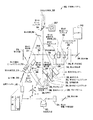
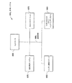
- 少なくとも1つのビーム経路に沿った連続照射を使用して、ウエハ上の測定部位の光学測定を実行するための第1のサブシステムと、
前記第1のサブシステムに隣接して取り付けられる第2のサブシステムであって、プローブ支持部によって支持されるプローブのセットを使用して、前記測定部位における伝導率の電気測定を実行するための第2のサブシステムと、
前記測定部位を前記第1のサブシステムおよび前記第2のサブシステムと整列させるために、平行移動ステージを動作させるためのコントローラと、
を備える、測定システム。 - 前記第1のサブシステムおよび前記第2のサブシステムは、真空、圧縮ガス、環境制御、および電力のうち少なくとも1つを含むサービスを共有する、請求項1に記載のシステム。
- 前記第1のサブシステムは、光音響測定システムを備える、請求項1に記載のシステム。
- 前記第2のサブシステムは、4点プローブシステムを備える、請求項1に記載のシステム。
- ウエハ上の測定部位の少なくとも1つのビーム経路に沿った連続照射を使用して、光学測定を実行するための第1のサブシステムと、
プローブ支持部によって支持されるプローブのセットを使用して、前記測定部位における伝導率の電気測定を実行するための第2のサブシステムとを備え、
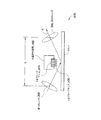
前記プローブ支持部は、光学測定中に前記プローブのセットをプローブ測定位置から非ブロック位置へ移動させるための手段を備える、
測定システム。 - 前記第1のサブシステムは、光音響測定システムを備える、請求項5に記載のシステム。
- 前記第2のサブシステムは、4点プローブシステムを備える、請求項5に記載のシステム。
- 前記プローブ支持部は、測定を行うために適所へ挿入するように適合される、請求項5に記載のシステム。
- 挿入は、水平射出、垂直下降、および片持下降のうち1つを含む、請求項8に記載のシステム。
- ウエハを測定する方法であって、
前記ウエハ上の測定部位のセットの第1の測定部位を、前記ウエハに当てる少なくとも1つのビーム経路に沿った連続照射を使用して光学測定を実行するための、第1のサブシステムの測定エリア内に位置させるステップと、
前記第1のサブシステムを使用して、光学測定データを生成するために、前記第1の測定部位において光学測定を行うステップと、
第2のサブシステムを使用して、伝導率測定データを生成するために、前記第1の測定部位において伝導率測定を行うステップと、
結果を形成するために、前記光学測定データと前記伝導率測定データとを組み合わせるステップと、
すべての測定部位について結果が形成されるまで、前記位置させるステップと、前記光学測定を行うステップと、前記伝導率測定を行うステップと、前記組み合わせるステップと、を繰り返すステップと、
を含む方法。 - 前記光学測定を行うステップは、光音響測定システムを動作させるステップを含む、請求項10に記載の方法。
- 前記伝導率測定を行うステップは、4点プローブシステムを動作させるステップを含む、請求項10に記載の方法。
- 前記ウエハを移送するステップおよび前記測定部位の少なくとも1つに位置させるステップのうち少なくとも1つのために、ロボットシステムを使用するステップをさらに含む、請求項10に記載の方法。
- 少なくとも1つの結果を適格とするための統計値を決定するステップをさらに含む、請求項10に記載の方法。
- 前記統計値は相関係数である、請求項14に記載の方法。
- 前記結果を調整するために前記統計値を使用するステップをさらに含む、請求項14に記載の方法。
- 前記第1のサブシステムおよび前記第2のサブシステムのうち少なくとも1つの調整を要求するために、前記統計値を使用するステップをさらに含む、請求項10に記載の方法。
- 前記伝導率測定を行うステップの前に、前記第2のサブシステムの測定エリア内に前記測定部位を位置させるステップをさらに含む、請求項10に記載の方法。
- 前記結果は、前記測定部位の厚さを代表するものである、請求項10に記載の方法。
- デュアル測定システムを動作させるための方法であって、
測定部位において、前記測定部位の少なくとも1つの特性に関する情報を識別するために、光音響システムによって測定を行うステップと、
前記情報を使用して、前記測定部位を評価するために、伝導率システムによって測定を行うステップと、
を含む方法。 - 前記少なくとも1つの特性は、接着、相互拡散、および層の欠落のうち少なくとも1つを含む、請求項20に記載の方法。
- 前記情報は、前記測定部位のバルク伝導率を含む、請求項20に記載の方法。
- 評価するステップは、適切な位相が形成されたか否かを判定するステップを含む、請求項20に記載の方法。
- ウエハ上の膜の厚さを決定する装置であって、光音響測定システムの測定領域内にウエハ上の測定部位を位置させ、その後4点プローブ測定システムの測定領域内に前記測定部位を位置させるための手段によって接続される、前記光音響測定システム及び前記4点プローブ測定システムを備え、前記光音響システムによって提供されるデータは、前記厚さを決定するために前記4点プローブシステムからのデータに相関せしめられる、装置。
- ウエハ上の膜の厚さを決定する装置であって、光音響測定システムの測定領域内にウエハ上の測定部位を位置させるための手段に接続され、且つ、4点プローブ測定システムの4点プローブヘッドアセンブリを挿入し、前記光音響測定システムの測定領域内の前記測定部位と電気的に接触させるための手段に接続される、前記光音響測定システムを備え、前記光音響システムによって提供されるデータは、前記厚さを決定するために前記4点プローブシステムからのデータに相関せしめられる、装置。
Applications Claiming Priority (2)
| Application Number | Priority Date | Filing Date | Title |
|---|---|---|---|
| US11/104,093 US7372584B2 (en) | 2005-04-11 | 2005-04-11 | Dual photo-acoustic and resistivity measurement system |
| PCT/US2006/010616 WO2006110282A2 (en) | 2005-04-11 | 2006-03-22 | Dual photo-acoustic and resistivity measurement system |
Publications (2)
| Publication Number | Publication Date |
|---|---|
| JP2008537781A true JP2008537781A (ja) | 2008-09-25 |
| JP2008537781A5 JP2008537781A5 (ja) | 2011-12-08 |
Family
ID=37082851
Family Applications (1)
| Application Number | Title | Priority Date | Filing Date |
|---|---|---|---|
| JP2008505351A Pending JP2008537781A (ja) | 2005-04-11 | 2006-03-22 | デュアル光音響および抵抗測定システム |
Country Status (4)
| Country | Link |
|---|---|
| US (1) | US7372584B2 (ja) |
| EP (1) | EP1869430A2 (ja) |
| JP (1) | JP2008537781A (ja) |
| WO (1) | WO2006110282A2 (ja) |
Cited By (1)
| Publication number | Priority date | Publication date | Assignee | Title |
|---|---|---|---|---|
| JP2014077782A (ja) * | 2012-09-20 | 2014-05-01 | National Institute Of Advanced Industrial & Technology | 焼き入れ深さ測定装置、焼き入れ深さ測定方法、表層深さ測定装置、表層深さ測定方法 |
Families Citing this family (7)
| Publication number | Priority date | Publication date | Assignee | Title |
|---|---|---|---|---|
| FR2887334B1 (fr) * | 2005-06-20 | 2007-08-24 | Centre Nat Rech Scient | Dispositif et procede de caracterisation de structure par effet de longueur d'onde dans un systeme photo-acoustique |
| US20070024870A1 (en) * | 2005-08-01 | 2007-02-01 | Girard Mark T | Apparatuses and methods for measuring head suspensions and head suspension assemblies |
| DE202010006062U1 (de) * | 2010-04-23 | 2010-07-22 | Helmut Fischer GmbH Institut für Elektronik und Messtechnik | Messsonde zur zerstörungsfreien Messung der Dicke dünner Schichten |
| CN102288825A (zh) * | 2011-06-08 | 2011-12-21 | 沈阳飞机工业(集团)有限公司 | 碳纤维复合材料制件表面铝层电阻值测量方法 |
| GB2503722A (en) * | 2012-07-06 | 2014-01-08 | Sonex Metrology Ltd | A photoacoustic inspection device |
| US9093335B2 (en) * | 2012-11-29 | 2015-07-28 | Taiwan Semiconductor Manufacturing Company, Ltd. | Calculating carrier concentrations in semiconductor Fins using probed resistance |
| US11668644B2 (en) | 2021-03-30 | 2023-06-06 | Onto Innovation Inc. | Opto-acoustic measurement of a transparent film stack |
Citations (5)
| Publication number | Priority date | Publication date | Assignee | Title |
|---|---|---|---|---|
| JPS6370102A (ja) * | 1986-09-10 | 1988-03-30 | Mitsubishi Petrochem Co Ltd | 導電体肉厚非破壊測定法 |
| JPS6375808U (ja) * | 1986-11-06 | 1988-05-20 | ||
| JPH09263934A (ja) * | 1996-03-29 | 1997-10-07 | Toppan Printing Co Ltd | 膜形成方法及びその装置 |
| JP2002516985A (ja) * | 1998-05-28 | 2002-06-11 | コーニンクレッカ フィリップス エレクトロニクス エヌ ヴィ | 少なくとも一つの層を含む構造の特徴を測定する方法及び装置 |
| JP2004325217A (ja) * | 2003-04-24 | 2004-11-18 | Nikon Corp | 搬送装置 |
Family Cites Families (15)
| Publication number | Priority date | Publication date | Assignee | Title |
|---|---|---|---|---|
| US3416078A (en) * | 1965-07-08 | 1968-12-10 | Motorola Inc | Method of determining resistivity of a thin layer |
| US3609537A (en) * | 1969-04-01 | 1971-09-28 | Ibm | Resistance standard |
| NL7008274A (ja) * | 1970-06-06 | 1971-12-08 | ||
| US3676775A (en) * | 1971-05-07 | 1972-07-11 | Ibm | Method for measuring resistivity |
| US3783375A (en) * | 1973-02-21 | 1974-01-01 | Westinghouse Electric Corp | Means for calibrating a four-probe resistivity measuring device |
| US4710030A (en) * | 1985-05-17 | 1987-12-01 | Bw Brown University Research Foundation | Optical generator and detector of stress pulses |
| US5379109A (en) * | 1992-06-17 | 1995-01-03 | The United States Of America As Represented By The Secretary Of The Navy | Method and apparatus for non-destructively measuring local resistivity of semiconductors |
| TW280928B (ja) * | 1994-10-24 | 1996-07-11 | At & T Corp | |
| US5546811A (en) * | 1995-01-24 | 1996-08-20 | Massachusetts Instittue Of Technology | Optical measurements of stress in thin film materials |
| US6008906A (en) * | 1995-08-25 | 1999-12-28 | Brown University Research Foundation | Optical method for the characterization of the electrical properties of semiconductors and insulating films |
| US5748318A (en) * | 1996-01-23 | 1998-05-05 | Brown University Research Foundation | Optical stress generator and detector |
| US5844684A (en) * | 1997-02-28 | 1998-12-01 | Brown University Research Foundation | Optical method for determining the mechanical properties of a material |
| US6038026A (en) * | 1998-07-07 | 2000-03-14 | Brown University Research Foundation | Apparatus and method for the determination of grain size in thin films |
| US6393915B1 (en) * | 1999-07-29 | 2002-05-28 | Koninklijke Philips Electronics N.V. | Method and device for simultaneously measuring multiple properties of multilayer films |
| US7050160B1 (en) * | 2002-10-11 | 2006-05-23 | Kla-Tencor Technologies Corporation | Process and apparatus for integrating sheet resistance measurements and reflectance measurements of a thin film in a common apparatus |
-
2005
- 2005-04-11 US US11/104,093 patent/US7372584B2/en active Active
-
2006
- 2006-03-22 EP EP06739420A patent/EP1869430A2/en not_active Withdrawn
- 2006-03-22 JP JP2008505351A patent/JP2008537781A/ja active Pending
- 2006-03-22 WO PCT/US2006/010616 patent/WO2006110282A2/en active Application Filing
Patent Citations (5)
| Publication number | Priority date | Publication date | Assignee | Title |
|---|---|---|---|---|
| JPS6370102A (ja) * | 1986-09-10 | 1988-03-30 | Mitsubishi Petrochem Co Ltd | 導電体肉厚非破壊測定法 |
| JPS6375808U (ja) * | 1986-11-06 | 1988-05-20 | ||
| JPH09263934A (ja) * | 1996-03-29 | 1997-10-07 | Toppan Printing Co Ltd | 膜形成方法及びその装置 |
| JP2002516985A (ja) * | 1998-05-28 | 2002-06-11 | コーニンクレッカ フィリップス エレクトロニクス エヌ ヴィ | 少なくとも一つの層を含む構造の特徴を測定する方法及び装置 |
| JP2004325217A (ja) * | 2003-04-24 | 2004-11-18 | Nikon Corp | 搬送装置 |
Cited By (1)
| Publication number | Priority date | Publication date | Assignee | Title |
|---|---|---|---|---|
| JP2014077782A (ja) * | 2012-09-20 | 2014-05-01 | National Institute Of Advanced Industrial & Technology | 焼き入れ深さ測定装置、焼き入れ深さ測定方法、表層深さ測定装置、表層深さ測定方法 |
Also Published As
| Publication number | Publication date |
|---|---|
| US20060227342A1 (en) | 2006-10-12 |
| US7372584B2 (en) | 2008-05-13 |
| WO2006110282A3 (en) | 2007-03-15 |
| EP1869430A2 (en) | 2007-12-26 |
| WO2006110282A2 (en) | 2006-10-19 |
Similar Documents
| Publication | Publication Date | Title |
|---|---|---|
| US5748317A (en) | Apparatus and method for characterizing thin film and interfaces using an optical heat generator and detector | |
| US6175416B1 (en) | Optical stress generator and detector | |
| US5748318A (en) | Optical stress generator and detector | |
| US6348967B1 (en) | Method and device for measuring the thickness of opaque and transparent films | |
| JP2008537781A (ja) | デュアル光音響および抵抗測定システム | |
| JP2008537781A5 (ja) | ||
| US6504618B2 (en) | Method and apparatus for decreasing thermal loading and roughness sensitivity in a photoacoustic film thickness measurement system | |
| US5228776A (en) | Apparatus for evaluating thermal and electrical characteristics in a sample | |
| KR100641271B1 (ko) | 집적 회로들의 특성화를 위한 광학적 방법 및 시스템 | |
| EP1417450B1 (en) | Method and apparatus for increasing signal to noise ratio in a photoacoustic film thickness measurement system | |
| US7027142B2 (en) | Optical technique for detecting buried defects in opaque films | |
| JP4025369B2 (ja) | 材料の機械的特性を判別する光学方法 | |
| JP4918634B2 (ja) | 光学計測システムを使用した誘電体薄膜の弾性係数の測定 | |
| US20220364850A1 (en) | Second-harmonic generation for critical dimensional metrology | |
| Liu et al. | A novel method and device for solder joint quality inspection by using laser ultrasound | |
| Badine et al. | Measurement of Thermal Properties and Interface Thermal Resistance of Thin Films by Thermoreflectance | |
| WO2023245019A1 (en) | Dimensional metrology using non-linear optics | |
| Logan et al. | Microelectronic Film thickness determination using a laserbased ultrasonic technique | |
| JP2001083068A (ja) | 近接場光学顕微鏡 |
Legal Events
| Date | Code | Title | Description |
|---|---|---|---|
| A621 | Written request for application examination |
Free format text: JAPANESE INTERMEDIATE CODE: A621 Effective date: 20090316 |
|
| A977 | Report on retrieval |
Free format text: JAPANESE INTERMEDIATE CODE: A971007 Effective date: 20110603 |
|
| A131 | Notification of reasons for refusal |
Free format text: JAPANESE INTERMEDIATE CODE: A131 Effective date: 20110613 |
|
| A601 | Written request for extension of time |
Free format text: JAPANESE INTERMEDIATE CODE: A601 Effective date: 20110908 |
|
| A602 | Written permission of extension of time |
Free format text: JAPANESE INTERMEDIATE CODE: A602 Effective date: 20110915 |
|
| A601 | Written request for extension of time |
Free format text: JAPANESE INTERMEDIATE CODE: A601 Effective date: 20111011 |
|
| A521 | Written amendment |
Free format text: JAPANESE INTERMEDIATE CODE: A523 Effective date: 20111013 |
|
| A524 | Written submission of copy of amendment under section 19 (pct) |
Free format text: JAPANESE INTERMEDIATE CODE: A524 Effective date: 20111013 |
|
| A602 | Written permission of extension of time |
Free format text: JAPANESE INTERMEDIATE CODE: A602 Effective date: 20111018 |
|
| A02 | Decision of refusal |
Free format text: JAPANESE INTERMEDIATE CODE: A02 Effective date: 20120305 |