US10069115B2 - Package method of substrate - Google Patents
Package method of substrate Download PDFInfo
- Publication number
- US10069115B2 US10069115B2 US15/105,570 US201615105570A US10069115B2 US 10069115 B2 US10069115 B2 US 10069115B2 US 201615105570 A US201615105570 A US 201615105570A US 10069115 B2 US10069115 B2 US 10069115B2
- Authority
- US
- United States
- Prior art keywords
- substrate
- cover plate
- seal
- package
- cutting line
- Prior art date
- Legal status (The legal status is an assumption and is not a legal conclusion. Google has not performed a legal analysis and makes no representation as to the accuracy of the status listed.)
- Active, expires
Links
Images


Classifications
-
- H—ELECTRICITY
- H10—SEMICONDUCTOR DEVICES; ELECTRIC SOLID-STATE DEVICES NOT OTHERWISE PROVIDED FOR
- H10K—ORGANIC ELECTRIC SOLID-STATE DEVICES
- H10K59/00—Integrated devices, or assemblies of multiple devices, comprising at least one organic light-emitting element covered by group H10K50/00
- H10K59/80—Constructional details
- H10K59/87—Passivation; Containers; Encapsulations
- H10K59/871—Self-supporting sealing arrangements
-
- H01L51/56—
-
- C—CHEMISTRY; METALLURGY
- C03—GLASS; MINERAL OR SLAG WOOL
- C03C—CHEMICAL COMPOSITION OF GLASSES, GLAZES OR VITREOUS ENAMELS; SURFACE TREATMENT OF GLASS; SURFACE TREATMENT OF FIBRES OR FILAMENTS MADE FROM GLASS, MINERALS OR SLAGS; JOINING GLASS TO GLASS OR OTHER MATERIALS
- C03C25/00—Surface treatment of fibres or filaments made from glass, minerals or slags
- C03C25/62—Surface treatment of fibres or filaments made from glass, minerals or slags by application of electric or wave energy; by particle radiation or ion implantation
- C03C25/6206—Electromagnetic waves
- C03C25/6226—Ultraviolet
-
- C—CHEMISTRY; METALLURGY
- C03—GLASS; MINERAL OR SLAG WOOL
- C03C—CHEMICAL COMPOSITION OF GLASSES, GLAZES OR VITREOUS ENAMELS; SURFACE TREATMENT OF GLASS; SURFACE TREATMENT OF FIBRES OR FILAMENTS MADE FROM GLASS, MINERALS OR SLAGS; JOINING GLASS TO GLASS OR OTHER MATERIALS
- C03C27/00—Joining pieces of glass to pieces of other inorganic material; Joining glass to glass other than by fusing
- C03C27/06—Joining glass to glass by processes other than fusing
-
- H01L51/52—
-
- H01L51/5237—
-
- H—ELECTRICITY
- H10—SEMICONDUCTOR DEVICES; ELECTRIC SOLID-STATE DEVICES NOT OTHERWISE PROVIDED FOR
- H10K—ORGANIC ELECTRIC SOLID-STATE DEVICES
- H10K50/00—Organic light-emitting devices
- H10K50/80—Constructional details
-
- H—ELECTRICITY
- H10—SEMICONDUCTOR DEVICES; ELECTRIC SOLID-STATE DEVICES NOT OTHERWISE PROVIDED FOR
- H10K—ORGANIC ELECTRIC SOLID-STATE DEVICES
- H10K50/00—Organic light-emitting devices
- H10K50/80—Constructional details
- H10K50/84—Passivation; Containers; Encapsulations
-
- H—ELECTRICITY
- H10—SEMICONDUCTOR DEVICES; ELECTRIC SOLID-STATE DEVICES NOT OTHERWISE PROVIDED FOR
- H10K—ORGANIC ELECTRIC SOLID-STATE DEVICES
- H10K50/00—Organic light-emitting devices
- H10K50/80—Constructional details
- H10K50/84—Passivation; Containers; Encapsulations
- H10K50/841—Self-supporting sealing arrangements
-
- H—ELECTRICITY
- H10—SEMICONDUCTOR DEVICES; ELECTRIC SOLID-STATE DEVICES NOT OTHERWISE PROVIDED FOR
- H10K—ORGANIC ELECTRIC SOLID-STATE DEVICES
- H10K71/00—Manufacture or treatment specially adapted for the organic devices covered by this subclass
-
- H—ELECTRICITY
- H10—SEMICONDUCTOR DEVICES; ELECTRIC SOLID-STATE DEVICES NOT OTHERWISE PROVIDED FOR
- H10K—ORGANIC ELECTRIC SOLID-STATE DEVICES
- H10K71/00—Manufacture or treatment specially adapted for the organic devices covered by this subclass
- H10K71/40—Thermal treatment, e.g. annealing in the presence of a solvent vapour
-
- H01L2251/566—
-
- H—ELECTRICITY
- H10—SEMICONDUCTOR DEVICES; ELECTRIC SOLID-STATE DEVICES NOT OTHERWISE PROVIDED FOR
- H10K—ORGANIC ELECTRIC SOLID-STATE DEVICES
- H10K71/00—Manufacture or treatment specially adapted for the organic devices covered by this subclass
- H10K71/851—Division of substrate
Definitions
- the present invention relates to a display technology field, and more particularly to a package method of a substrate.
- the panel display skill (LCD, OLED) has been gradually replaced the CRT displays.
- the flat light source technology is a new type light source and its skill development has been reached up for the mass production level of the market.
- the attachment of two sheet glasses is a very important skill. The package result directly influences the performance of the elements.
- UV curing technology is the earliest and the most common LCD/OLED package skill. It has properties below: no solvent or tiny solvent is used to reduce the pollution to the environment; less power consumption, low temperature curability is adaptable for the heat sensitive material; fast curing and high efficiency is applicable for the high speed production line, and the curing equipment merely occupies small space, etc.
- the seal height and the seal width of the seal which does not contain the spacers is very difficult to control. It is possible that the differences of the seal height and the seal width can be exist for the present set of glasses and the previous set of glasses, or inside the same set of the glasses.
- FIG. 1 is a diagram of a package method of a substrate according to prior art.
- the package method comprises steps of: step 1, coating the seal 300 which does not contain the spacers at the border position of the package cover plate 100 ; step 2, oppositely assembling the package cover plate 100 and the substrate 200 for packaging, and then solidifying the seal 300 for accomplishing the package to the substrate 200 .
- the seal 300 does not contain the spacers.
- the seal height and the seal width of the seal 300 is very difficult to control, and the seal height and the seal width of the seal 300 on various positions on the substrate 200 may not be uniform. Consequently, the tightness of the obtained package structure of the substrate is poor to lead to the failure of the package.
- An objective of the present invention is to provide a package method of a substrate, which utilizes seal which does not contain spacers for packaging the substrate, and ensures that the seal has the consistent height and width.
- the manufacture process is simple and easy, and the package result is great.
- the present invention provides a package method of a substrate, comprising steps of:
- step 1 providing a package cover plate and a substrate for packaging, and a first cutting line of a frame shape is located at a border position of the package cover plate, and a second cutting line of a frame shape is located at a border position of the substrate;
- step 2 forming a plurality of support parts which are separately located corresponding to a periphery of the first cutting line on the package cover plate, and meanwhile, the plurality of support parts are located corresponding to a periphery of the second cutting line on the substrate;
- step 3 coating a circle of seal corresponding to an inner side of the first cutting line on the package cover plate, and meanwhile, the seal is located corresponding to an inner side of the second cutting line on the substrate;
- step 4 para bonding the package cover plate and the substrate
- step 5 solidifying the seal
- step 6 cutting the package cover plate along the first cutting line, and cutting the substrate along the second cutting line to cut off the plurality of support parts, and border parts of the substrate and the package cover plate contacting with the plurality of support parts to achieve package of the package cover plate to the substrate.
- the package cover plate is a glass substrate; the substrate comprises a TFT substrate and an OLED element located on the TFT substrate, and the second cutting line is located corresponding to a periphery of the OLED element on the substrate.
- Material of the support part is an inorganic substance.
- a shape of the support part is a strip or a column.
- the plurality of support parts which are spaced enclose in a rectangular shape on the package cover plate.
- the heights of the support parts are 3-6 ⁇ m, and widths of the support parts are 0.1-10 mm.
- the seal is a seal which does not contain spacers.
- the seal is located corresponding to the OLED element and the second cutting line on the substrate.
- step 5 a method of heating or ultraviolet light irradiation is employed to solidify the seal.
- the present invention further provides a package method of a substrate, comprising steps of:
- step 1 providing a package cover plate and a substrate for packaging, and a first cutting line of a frame shape is located at a border position of the package cover plate, and a second cutting line of a frame shape is located at a border position of the substrate;
- step 2 forming a plurality of support parts which are separately located corresponding to a periphery of the first cutting line on the package cover plate, and meanwhile, the plurality of support parts are located corresponding to a periphery of the second cutting line on the substrate;
- step 3 coating a circle of seal corresponding to an inner side of the first cutting line on the package cover plate, and meanwhile, the seal is located corresponding to an inner side of the second cutting line on the substrate;
- step 4 para bonding the package cover plate and the substrate
- step 5 solidifying the seal
- step 6 cutting the package cover plate along the first cutting line, and cutting the substrate along the second cutting line to cut off the plurality of support parts, and border parts of the substrate and the package cover plate contacting with the plurality of support parts to achieve package of the package cover plate to the substrate;
- the package cover plate is a glass substrate;
- the substrate comprises a TFT substrate and an OLED element located on the TFT substrate, and the second cutting line is located corresponding to a periphery of the OLED element on the substrate;
- material of the support part is an inorganic substance
- a shape of the support part is a strip or a column
- the present invention provides a package method of a substrate.
- the gap of the package cover plate and the substrate is limited after para bonding the package cover plate and the substrate.
- the seal height of the seal which does not contain the spacers can be ensured, and under circumstance of certain seal coating volume, the seal width of the seal also can be ensured.
- the substrate packaged with the seal which does not contain the spacers can be obtained, and it is ensured that the seal has the consistent height and width.
- the manufacture process is simple and easy, and the package result is great.
- FIG. 1 is a diagram of a package method of a substrate according to prior art
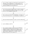
- FIG. 2 is a flowchart of a package method of a substrate according to the present invention.
- FIG. 3 is a structure diagram of a package cover plate provided in the step 1 of a package method of a substrate according to the present invention
- FIG. 4 is a structure diagram of a substrate for packaging provided in the step 1 of a package method of a substrate according to the present invention
- FIG. 5 is a diagram of the step 2 in a package method of a substrate according to the present invention.
- FIGS. 6-7 are diagrams of the step 3 in a package method of a substrate according to the present invention.
- FIG. 8 is a diagram of the steps 4-5 in a package method of a substrate according to the present invention.
- FIG. 9 is a diagram of the step 6 in a package method of a substrate according to the present invention.
- the present invention provides a package method of a substrate, comprising steps of:
- step 1 as shown in FIG. 3 and FIG. 4 , providing a package cover plate 10 and a substrate 20 for packaging, and a first cutting line 11 of a frame shape is located at a border position of the package cover plate 10 , and a second cutting line 21 of a frame shape is located at a border position of the substrate 20 .
- the package cover plate 10 is a glass substrate.
- the substrate 20 is an OLED substrate, comprising a TFT substrate 23 and an OLED element 25 located on the TFT substrate 23 , and the second cutting line 21 is located corresponding to a periphery of the OLED element 25 on the substrate 20 .
- step 2 as shown in FIG. 5 , forming a plurality of support parts 12 which are separately located corresponding to a periphery of the first cutting line 11 on the package cover plate 10 , and meanwhile, the plurality of support parts 12 are located corresponding to a periphery of the second cutting line 21 on the substrate 20 .
- material of the support part 12 is an inorganic substance, such as silicon oxide (SiO2), silicon nitride (SiNx), and etc.
- a shape of the support part 12 can be kinds of shapes, such as a strip (as shown in FIG. 5 ) or a column.
- the plurality of support parts 12 which are separately located enclose in a rectangular shape on the package cover plate 10 .
- the heights of the plurality of support parts 12 are equal. Specifically, the heights of the support parts 12 can be designed according to the gap of the upper, lower substrates for packaging.
- the heights of the support parts 12 are 3-6 ⁇ m, and widths of the support parts 12 are 0.1-10 mm.
- the plurality of support parts 12 are formed with a chemical vapor deposition process and a photolithographic process.
- step 3 coating a circle of seal 15 corresponding to an inner side of the first cutting line 11 on the package cover plate 10 , and meanwhile, the seal 15 is located corresponding to an inner side of the second cutting line 21 on the substrate 20 .
- the seal 15 is a seal which does not contain spacers.
- the seal 15 is correspondingly located between the OLED element 25 on the substrate 20 and the second cutting line 21 .
- step 4 para bonding the package cover plate 10 and the substrate 20 .
- step 5 solidifying the seal 15 .
- a method of heating or ultraviolet (UV) light irradiation is employed to solidify the seal 15 depending on the solidification condition of the seal 15 .
- step 6 as shown in FIG. 8 and FIG. 9 , cutting the package cover plate 10 along the first cutting line 11 , and cutting the substrate 20 along the second cutting line 21 to cut off the plurality of support parts 12 , and border parts of the substrate 20 and the package cover plate 10 contacting with the plurality of support parts 12 to achieve package of the package cover plate 10 to the substrate 20 .
- the present invention provides a package method of a substrate.
- the gap of the package cover plate and the substrate is limited after para bonding the package cover plate and the substrate.
- the seal height of the seal which does not contain the spacers can be ensured, and under circumstance of certain seal coating volume, the seal width of the seal also can be ensured.
- the substrate packaged with the seal which does not contain the spacers can be obtained, and it is ensured that the seal has the consistent height and width.
- the manufacture process is simple and easy, and the package result is great.
Landscapes
- Engineering & Computer Science (AREA)
- Chemical & Material Sciences (AREA)
- Physics & Mathematics (AREA)
- Life Sciences & Earth Sciences (AREA)
- Manufacturing & Machinery (AREA)
- Optics & Photonics (AREA)
- Materials Engineering (AREA)
- Geochemistry & Mineralogy (AREA)
- General Chemical & Material Sciences (AREA)
- Organic Chemistry (AREA)
- Chemical Kinetics & Catalysis (AREA)
- Electromagnetism (AREA)
- General Life Sciences & Earth Sciences (AREA)
- Ceramic Engineering (AREA)
- Electroluminescent Light Sources (AREA)
- Packaging Frangible Articles (AREA)
Applications Claiming Priority (4)
| Application Number | Priority Date | Filing Date | Title |
|---|---|---|---|
| CN201610152445.0A CN105810849B (zh) | 2016-03-17 | 2016-03-17 | 基板的封装方法 |
| CN201610152445.0 | 2016-03-17 | ||
| CN201610152445 | 2016-03-20 | ||
| PCT/CN2016/080188 WO2017156829A1 (zh) | 2016-03-17 | 2016-04-26 | 基板的封装方法 |
Publications (2)
| Publication Number | Publication Date |
|---|---|
| US20180102504A1 US20180102504A1 (en) | 2018-04-12 |
| US10069115B2 true US10069115B2 (en) | 2018-09-04 |
Family
ID=56454419
Family Applications (1)
| Application Number | Title | Priority Date | Filing Date |
|---|---|---|---|
| US15/105,570 Active 2036-11-15 US10069115B2 (en) | 2016-03-17 | 2016-04-26 | Package method of substrate |
Country Status (3)
| Country | Link |
|---|---|
| US (1) | US10069115B2 (zh) |
| CN (1) | CN105810849B (zh) |
| WO (1) | WO2017156829A1 (zh) |
Families Citing this family (7)
| Publication number | Priority date | Publication date | Assignee | Title |
|---|---|---|---|---|
| CN107275517A (zh) * | 2017-06-30 | 2017-10-20 | 京东方科技集团股份有限公司 | 一种显示基板及其制备方法和显示装置 |
| CN107507923B (zh) * | 2017-08-01 | 2019-12-03 | 京东方科技集团股份有限公司 | 一种丝网网版、封装方法、显示面板和显示装置 |
| CN108598294A (zh) * | 2018-07-05 | 2018-09-28 | 武汉华星光电半导体显示技术有限公司 | 一种oled器件的封装方法以及封装结构 |
| CN110048020B (zh) * | 2019-04-12 | 2020-04-03 | 昆山国显光电有限公司 | 显示面板及其制备方法、显示装置 |
| JP6696025B1 (ja) * | 2019-04-22 | 2020-05-20 | 信越エンジニアリング株式会社 | 貼合デバイスの貼り合わせ装置及び貼り合わせ方法並びに貼合デバイス |
| CN110429206B (zh) | 2019-08-07 | 2021-11-23 | 京东方科技集团股份有限公司 | 封装盖板、显示装置、显示面板及显示面板的封装方法 |
| CN111369904B (zh) * | 2020-04-08 | 2022-05-31 | 深圳市华星光电半导体显示技术有限公司 | 显示面板及其制作方法、显示装置 |
Citations (1)
| Publication number | Priority date | Publication date | Assignee | Title |
|---|---|---|---|---|
| CN104362243A (zh) | 2014-10-24 | 2015-02-18 | 深圳市华星光电技术有限公司 | 基板的封装方法及封装结构 |
Family Cites Families (7)
| Publication number | Priority date | Publication date | Assignee | Title |
|---|---|---|---|---|
| JP3980954B2 (ja) * | 2002-07-15 | 2007-09-26 | 日本電波工業株式会社 | 表面実装水晶発振器 |
| CN1214461C (zh) * | 2003-02-13 | 2005-08-10 | 台湾典范半导体股份有限公司 | Qfn型影像感测元件构装方法 |
| US7800303B2 (en) * | 2006-11-07 | 2010-09-21 | Corning Incorporated | Seal for light emitting display device, method, and apparatus |
| CN101355043B (zh) * | 2007-07-26 | 2010-07-21 | 精材科技股份有限公司 | 电子元件封装体及其制作方法 |
| CN201749442U (zh) * | 2010-06-30 | 2011-02-16 | 彩虹集团公司 | 一种具有触摸屏的有机发光器件 |
| CN102707509B (zh) * | 2012-06-13 | 2015-06-17 | 深圳市华星光电技术有限公司 | 液晶面板及其制造方法 |
| CN103367658B (zh) * | 2013-07-17 | 2016-08-31 | 深圳市华星光电技术有限公司 | 一种玻璃封装结构和封装方法 |
-
2016
- 2016-03-17 CN CN201610152445.0A patent/CN105810849B/zh active Active
- 2016-04-26 WO PCT/CN2016/080188 patent/WO2017156829A1/zh not_active Ceased
- 2016-04-26 US US15/105,570 patent/US10069115B2/en active Active
Patent Citations (1)
| Publication number | Priority date | Publication date | Assignee | Title |
|---|---|---|---|---|
| CN104362243A (zh) | 2014-10-24 | 2015-02-18 | 深圳市华星光电技术有限公司 | 基板的封装方法及封装结构 |
Non-Patent Citations (1)
| Title |
|---|
| Machine translation of CN104362243, Feb. 2018. * |
Also Published As
| Publication number | Publication date |
|---|---|
| CN105810849A (zh) | 2016-07-27 |
| WO2017156829A1 (zh) | 2017-09-21 |
| CN105810849B (zh) | 2018-03-30 |
| US20180102504A1 (en) | 2018-04-12 |
Similar Documents
| Publication | Publication Date | Title |
|---|---|---|
| US10069115B2 (en) | Package method of substrate | |
| US9559331B2 (en) | OLED package method and OLED package structure | |
| US9876191B2 (en) | OLED panel, packaging method thereof, and a display device | |
| US9530982B2 (en) | Packaging method and packaging structure of substrate | |
| US9508960B2 (en) | Method for packaging display device and apparatus therefor | |
| US20160343979A1 (en) | Oled (organic light emitting diode) packaging method and oled package structure | |
| US9466809B2 (en) | OLED packaging method and structure | |
| US20160248016A1 (en) | Substrate packaging method | |
| CN203365864U (zh) | 显示基板和显示面板 | |
| CN104536211B (zh) | 一种显示面板、显示装置及显示面板的制作方法 | |
| US9519189B2 (en) | Liquid crystal cell, method for fabricating the same and display device | |
| JP2016531384A (ja) | ガラス封止構造体と封止方法 | |
| US20160248042A1 (en) | Oled package method and oled package structure | |
| CN104035239A (zh) | 一种基板及显示器件 | |
| US20150138470A1 (en) | Liquid crystal display panel and method of manufacturing the same | |
| US20130340583A1 (en) | Liquid Crystal Substrate Cutting Device and Cutting Method for Liquid Crystal Substrate | |
| CN104698695A (zh) | 一种显示基板及其制造方法、液晶显示装置 | |
| CN203287658U (zh) | 彩膜基板、液晶面板及显示装置 | |
| CN103744216A (zh) | 一种液晶显示面板及其制作方法 | |
| US10707439B2 (en) | Packaging adhesive, packaging method, display panel and display device | |
| US20150255750A1 (en) | Package Substrate, OLED Display Panel and Manufacturing Method Thereof, and Display Apparatus | |
| TWM512144U (zh) | 顯示面板 | |
| US9698376B2 (en) | Packaging method and packaging structure of substrate | |
| CN103913901B (zh) | 显示面板及显示面板的制作方法 | |
| CN104536192A (zh) | 一种液晶面板基板及其制造方法 |
Legal Events
| Date | Code | Title | Description |
|---|---|---|---|
| AS | Assignment |
Owner name: SHENZHEN CHINA STAR OPTOELECTRONICS TECHNOLOGY CO. Free format text: ASSIGNMENT OF ASSIGNORS INTEREST;ASSIGNOR:LIU, YAWEI;REEL/FRAME:038938/0036 Effective date: 20160524 |
|
| STCF | Information on status: patent grant |
Free format text: PATENTED CASE |
|
| MAFP | Maintenance fee payment |
Free format text: PAYMENT OF MAINTENANCE FEE, 4TH YEAR, LARGE ENTITY (ORIGINAL EVENT CODE: M1551); ENTITY STATUS OF PATENT OWNER: LARGE ENTITY Year of fee payment: 4 |
|
| MAFP | Maintenance fee payment |
Free format text: PAYMENT OF MAINTENANCE FEE, 8TH YEAR, LARGE ENTITY (ORIGINAL EVENT CODE: M1552); ENTITY STATUS OF PATENT OWNER: LARGE ENTITY Year of fee payment: 8 |