TWI775699B - Polishing pad and method of forming the same - Google Patents
Polishing pad and method of forming the same Download PDFInfo
- Publication number
- TWI775699B TWI775699B TW110148066A TW110148066A TWI775699B TW I775699 B TWI775699 B TW I775699B TW 110148066 A TW110148066 A TW 110148066A TW 110148066 A TW110148066 A TW 110148066A TW I775699 B TWI775699 B TW I775699B
- Authority
- TW
- Taiwan
- Prior art keywords
- features
- polishing pad
- polishing
- pad
- abrasive
- Prior art date
Links
Images


Classifications
-
- B—PERFORMING OPERATIONS; TRANSPORTING
- B24—GRINDING; POLISHING
- B24D—TOOLS FOR GRINDING, BUFFING OR SHARPENING
- B24D18/00—Manufacture of grinding tools or other grinding devices, e.g. wheels, not otherwise provided for
- B24D18/0045—Manufacture of grinding tools or other grinding devices, e.g. wheels, not otherwise provided for by stacking sheets of abrasive material
-
- B—PERFORMING OPERATIONS; TRANSPORTING
- B24—GRINDING; POLISHING
- B24B—MACHINES, DEVICES, OR PROCESSES FOR GRINDING OR POLISHING; DRESSING OR CONDITIONING OF ABRADING SURFACES; FEEDING OF GRINDING, POLISHING, OR LAPPING AGENTS
- B24B37/00—Lapping machines or devices; Accessories
- B24B37/11—Lapping tools
- B24B37/20—Lapping pads for working plane surfaces
- B24B37/205—Lapping pads for working plane surfaces provided with a window for inspecting the surface of the work being lapped
-
- B—PERFORMING OPERATIONS; TRANSPORTING
- B24—GRINDING; POLISHING
- B24B—MACHINES, DEVICES, OR PROCESSES FOR GRINDING OR POLISHING; DRESSING OR CONDITIONING OF ABRADING SURFACES; FEEDING OF GRINDING, POLISHING, OR LAPPING AGENTS
- B24B37/00—Lapping machines or devices; Accessories
- B24B37/11—Lapping tools
- B24B37/20—Lapping pads for working plane surfaces
- B24B37/22—Lapping pads for working plane surfaces characterised by a multi-layered structure
-
- B—PERFORMING OPERATIONS; TRANSPORTING
- B24—GRINDING; POLISHING
- B24B—MACHINES, DEVICES, OR PROCESSES FOR GRINDING OR POLISHING; DRESSING OR CONDITIONING OF ABRADING SURFACES; FEEDING OF GRINDING, POLISHING, OR LAPPING AGENTS
- B24B37/00—Lapping machines or devices; Accessories
- B24B37/11—Lapping tools
- B24B37/20—Lapping pads for working plane surfaces
- B24B37/24—Lapping pads for working plane surfaces characterised by the composition or properties of the pad materials
-
- B—PERFORMING OPERATIONS; TRANSPORTING
- B24—GRINDING; POLISHING
- B24B—MACHINES, DEVICES, OR PROCESSES FOR GRINDING OR POLISHING; DRESSING OR CONDITIONING OF ABRADING SURFACES; FEEDING OF GRINDING, POLISHING, OR LAPPING AGENTS
- B24B37/00—Lapping machines or devices; Accessories
- B24B37/11—Lapping tools
- B24B37/20—Lapping pads for working plane surfaces
- B24B37/26—Lapping pads for working plane surfaces characterised by the shape of the lapping pad surface, e.g. grooved
-
- B—PERFORMING OPERATIONS; TRANSPORTING
- B24—GRINDING; POLISHING
- B24D—TOOLS FOR GRINDING, BUFFING OR SHARPENING
- B24D18/00—Manufacture of grinding tools or other grinding devices, e.g. wheels, not otherwise provided for
- B24D18/0018—Manufacture of grinding tools or other grinding devices, e.g. wheels, not otherwise provided for by electrolytic deposition
-
- B—PERFORMING OPERATIONS; TRANSPORTING
- B24—GRINDING; POLISHING
- B24D—TOOLS FOR GRINDING, BUFFING OR SHARPENING
- B24D3/00—Physical features of abrasive bodies, or sheets, e.g. abrasive surfaces of special nature; Abrasive bodies or sheets characterised by their constituents
- B24D3/02—Physical features of abrasive bodies, or sheets, e.g. abrasive surfaces of special nature; Abrasive bodies or sheets characterised by their constituents the constituent being used as bonding agent
- B24D3/04—Physical features of abrasive bodies, or sheets, e.g. abrasive surfaces of special nature; Abrasive bodies or sheets characterised by their constituents the constituent being used as bonding agent and being essentially inorganic
- B24D3/14—Physical features of abrasive bodies, or sheets, e.g. abrasive surfaces of special nature; Abrasive bodies or sheets characterised by their constituents the constituent being used as bonding agent and being essentially inorganic ceramic, i.e. vitrified bondings
- B24D3/18—Physical features of abrasive bodies, or sheets, e.g. abrasive surfaces of special nature; Abrasive bodies or sheets characterised by their constituents the constituent being used as bonding agent and being essentially inorganic ceramic, i.e. vitrified bondings for porous or cellular structure
-
- B—PERFORMING OPERATIONS; TRANSPORTING
- B24—GRINDING; POLISHING
- B24D—TOOLS FOR GRINDING, BUFFING OR SHARPENING
- B24D3/00—Physical features of abrasive bodies, or sheets, e.g. abrasive surfaces of special nature; Abrasive bodies or sheets characterised by their constituents
- B24D3/02—Physical features of abrasive bodies, or sheets, e.g. abrasive surfaces of special nature; Abrasive bodies or sheets characterised by their constituents the constituent being used as bonding agent
- B24D3/20—Physical features of abrasive bodies, or sheets, e.g. abrasive surfaces of special nature; Abrasive bodies or sheets characterised by their constituents the constituent being used as bonding agent and being essentially organic
- B24D3/22—Rubbers synthetic or natural
-
- B—PERFORMING OPERATIONS; TRANSPORTING
- B29—WORKING OF PLASTICS; WORKING OF SUBSTANCES IN A PLASTIC STATE IN GENERAL
- B29C—SHAPING OR JOINING OF PLASTICS; SHAPING OF MATERIAL IN A PLASTIC STATE, NOT OTHERWISE PROVIDED FOR; AFTER-TREATMENT OF THE SHAPED PRODUCTS, e.g. REPAIRING
- B29C64/00—Additive manufacturing, i.e. manufacturing of three-dimensional [3D] objects by additive deposition, additive agglomeration or additive layering, e.g. by 3D printing, stereolithography or selective laser sintering
- B29C64/10—Processes of additive manufacturing
- B29C64/106—Processes of additive manufacturing using only liquids or viscous materials, e.g. depositing a continuous bead of viscous material
- B29C64/112—Processes of additive manufacturing using only liquids or viscous materials, e.g. depositing a continuous bead of viscous material using individual droplets, e.g. from jetting heads
-
- B—PERFORMING OPERATIONS; TRANSPORTING
- B33—ADDITIVE MANUFACTURING TECHNOLOGY
- B33Y—ADDITIVE MANUFACTURING, i.e. MANUFACTURING OF THREE-DIMENSIONAL [3-D] OBJECTS BY ADDITIVE DEPOSITION, ADDITIVE AGGLOMERATION OR ADDITIVE LAYERING, e.g. BY 3-D PRINTING, STEREOLITHOGRAPHY OR SELECTIVE LASER SINTERING
- B33Y10/00—Processes of additive manufacturing
-
- B—PERFORMING OPERATIONS; TRANSPORTING
- B33—ADDITIVE MANUFACTURING TECHNOLOGY
- B33Y—ADDITIVE MANUFACTURING, i.e. MANUFACTURING OF THREE-DIMENSIONAL [3-D] OBJECTS BY ADDITIVE DEPOSITION, ADDITIVE AGGLOMERATION OR ADDITIVE LAYERING, e.g. BY 3-D PRINTING, STEREOLITHOGRAPHY OR SELECTIVE LASER SINTERING
- B33Y80/00—Products made by additive manufacturing
Abstract
Description
本文揭示的實施例大體而言係關於化學機械研磨(CMP)製程中使用的研磨物件之製造。更具體言之,本文揭示的實施例係關於複合研磨墊。Embodiments disclosed herein relate generally to the manufacture of abrasive articles used in chemical mechanical polishing (CMP) processes. More specifically, the embodiments disclosed herein relate to composite polishing pads.
化學機械研磨(CMP)普遍用於在半導體元件的製造過程中平坦化基板。在CMP過程中,將被處理的基板固定在承載頭上,且使元件表面對著旋轉的研磨墊放置。承載頭在基板上提供可控制的負載,以對著研磨墊推壓元件表面。通常將研磨液(例如具有研磨顆粒的漿料)供應到研磨墊的表面。研磨墊是消耗品,因為在研磨某些數量的基板之後通常會被磨損並需要更換。Chemical Mechanical Polishing (CMP) is commonly used to planarize substrates during the fabrication of semiconductor devices. During CMP, the substrate being processed is held on a carrier head and the component surface is placed against a rotating polishing pad. The carrier head provides a controllable load on the substrate to push the component surface against the polishing pad. A polishing liquid, such as a slurry with abrasive particles, is typically supplied to the surface of the polishing pad. Polishing pads are consumables because they typically wear out and need to be replaced after polishing a certain number of substrates.
研磨墊通常是藉由模製、鑄造或燒結聚氨甲酸乙酯材料製成的。在模製的情況下,研磨墊可在一個時間製成,例如藉由注射成型。在鑄造的情況下,將液體前驅物澆鑄及固化成餅狀物,隨後該餅狀物被切成個別的墊片。然後,這些墊片可以被加工成最終的厚度。凹槽可以被加工到研磨表面中,或作為注射成型製程的一部分被形成。這些製造研磨墊的方法昂貴又耗時。藉由這些方法製造的研磨墊往往會產生不均勻的研磨結果。例如,在CMP過程中,基板上的不同區域可能會被以不同的速率研磨,導致一些區域中過多的材料被去除(「過度研磨」)或其他區域中太少的材料被去除(「研磨不足」)。Polishing pads are typically made by molding, casting, or sintering polyurethane materials. In the case of molding, the polishing pad can be made at one time, for example by injection molding. In the case of casting, the liquid precursor is cast and solidified into a cake, which is then cut into individual gaskets. These spacers can then be machined to their final thickness. The grooves can be machined into the ground surface, or formed as part of an injection molding process. These methods of making polishing pads are expensive and time-consuming. The polishing pads manufactured by these methods tend to produce uneven polishing results. For example, during a CMP process, different areas on a substrate may be ground at different rates, resulting in too much material being removed in some areas ("overgrinding") or too little material being removed in others ("undergrinding"). ”).
因此,需要一種提供改良的研磨均勻性的研磨墊及用於製作改良的研磨墊的方法。Accordingly, there is a need for a polishing pad that provides improved polishing uniformity and a method for making the improved polishing pad.
本揭示之實施例大體而言提供包括複合襯墊主體的研磨墊及形成該研磨墊的方法。Embodiments of the present disclosure generally provide polishing pads including composite pad bodies and methods of forming the same.
一個實施例提供包括複合襯墊主體的研磨墊。該複合襯墊主體包括一個或更多個由第一材料或第一材料組成物形成的第一特徵,及一個或更多個由第二材料或第二材料組成物形成的第二特徵,其中該一個或更多個第一特徵和該一個或更多個第二特徵是藉由沉積複數個包含該第一材料或第一材料組成物和第二材料或第二材料組成物的層所形成的。One embodiment provides a polishing pad including a composite pad body. The composite liner body includes one or more first features formed of a first material or composition of first materials and one or more second features formed of a second material or composition of second materials, wherein The one or more first features and the one or more second features are formed by depositing a plurality of layers comprising the first material or first material composition and a second material or second material composition of.
另一個實施例提供一種形成研磨墊的方法。該方法包括使用3D列印機沉積複數個複合層,直到達到目標厚度。沉積該複數個複合層中的每個層包含以下步驟:在一個或更多個第一區域上沉積第一材料或第一材料組成物,及在該一個或更多個第二區域上沉積第二材料或第二材料組成物,其中該一個或更多個第一區域及該一個或更多個第二區域形成連續區域。該方法進一步包括固化該等複合層以形成複合襯墊主體,該複合襯墊主體具有一個或更多個該第一材料或第一材料組成物之第一特徵及一個或更多個該第二材料或第二材料組成物之第二特徵,其中該一個或更多個第一特徵和該一個或更多個第二特徵形成單一主體。Another embodiment provides a method of forming a polishing pad. The method involves depositing a plurality of composite layers using a 3D printer until a target thickness is reached. Deposition of each of the plurality of composite layers comprises the steps of: depositing a first material or first material composition on one or more first regions, and depositing a first material on the one or more second regions A two-material or second material composition, wherein the one or more first regions and the one or more second regions form a continuous region. The method further includes curing the composite layers to form a composite liner body having one or more first features of the first material or first material composition and one or more of the second A second feature of a material or a second composition of materials, wherein the one or more first features and the one or more second features form a single body.
另一個實施例提供一種具有複合襯墊主體的研磨墊。該複合襯墊主體包括形成研磨表面的複數個研磨特徵,其中該複數個研磨特徵係由第一材料形成;以及一個或更多個由第二材料形成的基部特徵,其中該一個或更多個基部特徵聯合圍繞該複數個研磨特徵以形成單一主體。Another embodiment provides a polishing pad having a composite pad body. The composite liner body includes a plurality of abrasive features forming an abrasive surface, wherein the plurality of abrasive features are formed of a first material; and one or more base features formed of a second material, wherein the one or more The base feature jointly surrounds the plurality of abrasive features to form a single body.
一個實施例提供包含複合研磨襯墊主體的研磨墊。該複合研磨主體包含一個或更多個由第一材料形成的第一特徵,及一個或更多個由第二材料形成的第二特徵。該一個或更多個第一特徵和該一個或更多個第二特徵是藉由沉積複數個包含該第一材料和該第二材料的層所形成的。One embodiment provides a polishing pad including a composite polishing pad body. The composite abrasive body includes one or more first features formed from a first material and one or more second features formed from a second material. The one or more first features and the one or more second features are formed by depositing a plurality of layers comprising the first material and the second material.
在一個實施例中,該第一材料包含第一材料組成物,該第一材料組成物係藉由沉積第三材料和第四材料的液滴所形成的。在一個實施例中,該第二材料包含第二材料組成物,該第二材料組成物係藉由沉積第五材料和第六材料的液滴所形成的。In one embodiment, the first material comprises a first material composition formed by depositing droplets of a third material and a fourth material. In one embodiment, the second material comprises a second material composition formed by depositing droplets of the fifth material and the sixth material.
又另一個實施例提供一種形成研磨墊的方法。該方法包括使用3D列印機沉積複數個複合層,以達到目標厚度。沉積該複數個複合層包含以下步驟:在表面的一個或更多個第一區域上沉積第一材料,及在該表面的一個或更多個第二區域上沉積第二材料,其中該一個或更多個第一區域及該一個或更多個第二區域形成該複數個複合層之每一層的連續部分。該方法進一步包括固化該複數個複合層以形成複合襯墊主體,該複合襯墊主體具有一個或更多個包含該第一材料的第一特徵及一個或更多個包含該第二材料的第二特徵。該一個或更多個第一特徵和該一個或更多個第二特徵形成單一主體。Yet another embodiment provides a method of forming a polishing pad. The method involves depositing a plurality of composite layers using a 3D printer to achieve a target thickness. Depositing the plurality of composite layers comprises the steps of: depositing a first material on one or more first regions of a surface, and depositing a second material on one or more second regions of the surface, wherein the one or more The more first regions and the one or more second regions form a continuous portion of each of the plurality of composite layers. The method further includes curing the plurality of composite layers to form a composite liner body having one or more first features comprising the first material and one or more first features comprising the second material Two characteristics. The one or more first features and the one or more second features form a single body.
本揭示係關於研磨物件及製造該研磨物件之方法、以及研磨基板及在研磨基板之前、過程中及之後調理研磨物件的方法。The present disclosure pertains to abrasive articles and methods of making the same, as well as methods of lapping a substrate and conditioning the abrasive article before, during, and after lapping the substrate.
本揭示的實施例提供具有複合襯墊主體的研磨墊。複合襯墊主體包括由至少兩種不同的材料形成的個別特徵。依據本揭示的實施例,研磨墊可以藉由三維(3D)列印製程生產。例如,複合襯墊主體可以以3D列印機藉由連續沉積複數個層來形成,其中每一層包含不同材料或不同材料組成物的區域。在一些實施例中,然後該複數個層可以藉由硬化處理而被固化。複合襯墊主體中的個別特徵可以同時由不同材料或不同材料組成物形成。3D列印的沉積和硬化製程允許個別的特徵被牢固地接合在一起。個別特徵的幾何形狀可以使用3D列印製程輕易地控制。藉由選擇不同的材料或不同的材料組成物,個別的特徵可以具有不同的機械、物理、化學、及/或幾何性質,以獲得目標的襯墊性質。在一個實施例中,複合主體可以由具有不同機械性質的黏彈性材料形成。例如,複合主體可以由具有不同存儲模數及不同損耗模數的黏彈性材料形成。結果,複合襯墊主體可以包括一些由第一材料或第一材料組成物形成的彈性特徵及一些由比該第一材料或該第一材料組成物更硬的第二材料或第二材料組成物形成的硬特徵。Embodiments of the present disclosure provide polishing pads having composite pad bodies. The composite pad body includes individual features formed from at least two different materials. According to embodiments of the present disclosure, polishing pads may be produced by a three-dimensional (3D) printing process. For example, a composite liner body may be formed with a 3D printer by successively depositing a plurality of layers, where each layer includes a region of a different material or composition of a different material. In some embodiments, the plurality of layers may then be cured by a hardening process. Individual features in the composite liner body may be formed from different materials or different material compositions at the same time. The deposition and hardening process of 3D printing allows individual features to be firmly bonded together. The geometry of individual features can be easily controlled using the 3D printing process. By selecting different materials or different material compositions, individual features can have different mechanical, physical, chemical, and/or geometric properties to achieve targeted pad properties. In one embodiment, the composite body may be formed from viscoelastic materials with different mechanical properties. For example, the composite body may be formed from viscoelastic materials having different storage moduli and different loss moduli. As a result, the composite pad body may include some elastic features formed from a first material or composition of first materials and some formed from a second material or composition of materials that are harder than the first material or composition of first materials hard features.
第1圖為研磨站100的示意性剖視圖。研磨站100可被用於研磨系統,以進行基板研磨。研磨站100包括平臺102。平臺102可以圍繞中心軸104旋轉。研磨墊106可被放在平臺102上。依據本揭示的實施例,研磨墊106可以包括複合研磨主體。研磨墊106包括設以接觸和處理基板的研磨表面112。平臺102支撐研磨墊106並在研磨期間旋轉研磨墊106。承載頭108可以對著研磨墊106的研磨表面112固持被處理的基板110。承載頭108可以圍繞中心軸114旋轉及/或以掃過的動作移動,以在基板110和研磨墊106之間產生相對運動。在研磨過程中,可以將諸如研磨漿的研磨流體116藉由輸送臂118供應到研磨表面112。研磨液116可以含有研磨顆粒、酸鹼度調節劑及/或化學活性成份,以致能基板的化學機械研磨。
研磨墊 FIG. 1 is a schematic cross-sectional view of a
第2A圖為依據本揭示之一個實施例的研磨墊200之示意性立體剖視圖。研磨墊200可被用於研磨站,例如研磨站100,用於藉由化學機械研磨研磨基板。FIG. 2A is a schematic perspective cross-sectional view of a
研磨墊200包括複合襯墊主體202。複合襯墊主體202包括一個或更多個硬特徵204及一個或更多個彈性特徵206。硬特徵204和彈性特徵206是邊界被接合在一起以形成複合襯墊主體202的個別特徵。在一個實施例中,硬特徵204可以具有約40蕭氏D級至約90蕭氏D級的硬度。彈性特徵206可以具有介於約26蕭氏A級至約95蕭氏A級之間的硬度值。The
複合襯墊主體202可以藉由3D列印或其他適當的技術形成。複合襯墊主體202可以包括複數個層,其中依據複合襯墊主體202的設計,每一層包括藉由3D列印機沉積的彈性特徵206區域及/或硬特徵204區域。然後該複數個層可以被硬化,例如藉由UV光或藉由熱源,以固化並實現目標硬度。沉積和硬化之後便形成了包括被耦接或接合在一起的硬特徵204和彈性特徵206的單一複合襯墊主體202。
可以選擇具有不同機械性質的材料用於彈性特徵206和硬特徵204,以實現目標的研磨製程。彈性特徵206和硬特徵204的動態機械性質可以藉由選擇不同的材料及/或選擇特徵形成製程過程中使用的不同硬化製程來實現。在一個實施例中,彈性特徵206可以具有較低的硬度值和較低的楊氏模數值,而硬特徵204可以具有較高的硬度值和較高的楊氏模數值。在另一個實施例中,諸如存儲模數和損耗模數等動態機械性質可以在每個特徵內被調整或控制及/或藉由彈性特徵206和硬特徵204在研磨墊的研磨表面內或各處的實體佈局、圖案或組合來調整或控制。Materials with different mechanical properties can be selected for
硬特徵204可以由一種或更多種聚合物材料形成。硬特徵204可以由單一聚合物材料或兩種或更多種聚合物的混合物形成,以實現目標性質。在一個實施例中,硬特徵204可以由一種或更多種熱塑性聚合物形成。硬特徵204可以由熱塑性聚合物形成,例如聚氨甲酸乙酯、聚丙烯、聚苯乙烯、聚丙烯腈、聚甲基丙烯酸甲酯、聚氯三氟乙烯、聚四氟乙烯、聚甲醛、聚碳酸酯、聚醯亞胺、聚醚醚酮、聚伸苯硫、聚醚碸、丙烯腈丁二烯苯乙烯(ABS)、聚醚醯亞胺、聚醯胺、三聚氰胺、聚酯、聚碸、聚乙酸乙烯酯、氟化烴等等、以及丙烯酸酯、上述之共聚物、移植物、及混合物。在一個實施例中,硬特徵204可以由丙烯酸酯形成。例如,硬特徵204可以是聚氨甲酸乙酯丙烯酸酯、聚醚丙烯酸酯、或聚酯丙烯酸酯。在另一個實施例中,硬特徵204可以包括一種或更多種熱固性聚合物,例如環氧樹脂、酚醛樹脂、胺類、聚酯、胺甲酸乙酯、矽、以及丙烯酸酯、上述之混合物、共聚物及移植物。Hard features 204 may be formed from one or more polymeric materials. Hard features 204 may be formed from a single polymeric material or a mixture of two or more polymers to achieve target properties. In one embodiment,
在一個實施例中,硬特徵可以由模擬塑膠3D列印材料形成。在一個實施例中,研磨顆粒可以被嵌入硬特徵204中,以增強研磨製程。包含研磨顆粒的材料可以是金屬氧化物,例如氧化鈰、氧化鋁、二氧化矽、或上述之組合、聚合物、介金屬或陶瓷。In one embodiment, the hard features may be formed from a simulated plastic 3D printed material. In one embodiment, abrasive particles may be embedded in
彈性特徵206可以由一種或更多種聚合物材料形成。彈性特徵206可以由單一聚合物材料或兩種以上的聚合物之混合物形成,以實現目標性質。在一個實施例中,彈性特徵206可以由一種或更多種熱塑性聚合物形成。例如,彈性特徵206可以由熱塑性聚合物形成,例如聚氨甲酸乙酯、聚丙烯、聚苯乙烯、聚丙烯腈、聚甲基丙烯酸甲酯、聚氯三氟乙烯、聚四氟乙烯、聚甲醛、聚碳酸酯、聚醯亞胺、聚醚醚酮、聚伸苯硫、聚醚碸、丙烯腈丁二烯苯乙烯(ABS)、聚醚醯亞胺、聚醯胺、三聚氰胺、聚酯、聚碸、聚乙酸乙烯酯、氟化烴等等、以及丙烯酸酯、上述之共聚物、移植物、及混合物。在一個實施例中,彈性特徵206可以由丙烯酸酯形成。例如,彈性特性206可以是聚氨甲酸乙酯丙烯酸酯、聚醚丙烯酸酯、或聚酯丙烯酸酯。在另一個實施例中,彈性特徵206可以由熱塑性彈性體形成。在一個實施例中,彈性特徵206可以由類橡膠3D列印材料形成。The elastic features 206 may be formed from one or more polymeric materials. The elastic features 206 may be formed from a single polymeric material or a mixture of two or more polymers to achieve target properties. In one embodiment, the
硬特徵204通常比彈性特徵206更硬且更剛性,而彈性特徵206比硬特徵204更柔軟且更彈性。可以選擇硬特徵204和彈性特徵206的材料和圖案,以實現研磨墊200的「調整」塊體材料。使用此「調整」塊體材料形成的研磨墊200具有各種優點,例如改良的研磨結果、降低的製造成本、延長的襯墊壽命。在一個實施例中,「調整」塊體材料或研磨墊整體可以具有介於約65蕭氏A至約75蕭氏D之間的硬度。研磨墊的拉伸強度可以介於5 MPa至約75 MPa之間。研磨墊可以具有約5 %至約350 %的斷裂伸長率。研磨墊可以具有高於約10m Pa的剪切強度。研磨墊可以具有介於約5 MPa至約2000 MPa之間的存儲模數。研磨墊在25 ℃至90 ℃的溫度範圍間可以具有穩定的存儲模數,使得E30/E90的存儲模數比率落在約6至約30間的範圍內,其中E30是在30 ℃下的存儲模數,而E90是在90 ℃下的存儲模數。Hard features 204 are generally stiffer and more rigid than
在一個實施例中,硬特徵204和彈性特徵206的材料對於研磨漿具有耐化學侵蝕性。在另一個實施例中,硬特徵204和彈性特徵206的材料是親水性的。In one embodiment, the materials of
在一個實施例中,硬特徵204和彈性特徵206可以是被交替排列以形成圓形複合襯墊主體202的交替同心環。在一個實施例中,硬特徵204的高度210高於彈性特徵206的高度212,使得硬特徵204的上表面208從彈性特徵206突出。凹槽218或通道被形成在硬特徵204和彈性特徵206之間。在研磨過程中,硬特徵204的上表面208形成接觸基板的研磨表面,而凹槽218保留研磨流體。在一個實施例中,硬特徵204在垂直於平行複合襯墊主體202的平面的方向上比彈性特徵206更厚,使得凹槽218及/或通道被形成在複合襯墊主體202的頂表面上。In one embodiment, the
在一個實施例中,硬特徵204的寬度214可以介於約250微米至約2毫米之間。硬特徵204之間的間距216可以介於約0.5毫米至約5毫米之間。每個硬特徵204可以具有在約250微米至約2毫米間的範圍內的寬度。寬度214及/或間距216可以橫跨研磨墊200的半徑變化到不同硬度的區域。In one embodiment, the
與傳統的研磨墊相比,本揭示的複合研磨墊200具有幾個優點。通常傳統的研磨墊包括的研磨層具有紋理化的研磨表面及/或由軟質材料(例如泡沫材料)形成的子墊支撐的研磨材料,以獲得用於研磨基板的目標硬度或楊氏模數。藉由選擇具有各種機械性質(例如楊氏模數、存儲模數及損耗模數)的材料及調整特徵的尺寸和間距或改變不同特徵的配置,可以在不使用子墊之下在複合襯墊主體202中實現理想的硬度、動態性質及/或機械性質。因此,研磨墊200藉由免除子墊而降低了所有權成本。此外,研磨墊200的硬度和研磨性可以藉由混合具有不同硬度和研磨性的特徵來調整,從而改良研磨性能。The
依據本揭示的複合研磨墊可以藉由圖案變化及/或特徵尺寸的變化而在表面特徵(例如硬特徵204)和基材(例如彈性特徵206)各處具有可變的機械性質,例如楊氏模數或存儲模數及損耗模數。在研磨墊各處的機械性質可以是對稱或是非對稱的、均勻或不均勻的,以實現目標性質。依據實現的目標性質,例如預定的機械性質,例如楊氏模數或存儲模數和損耗模數,在研磨墊各處的表面特徵之圖案可以是放射狀的、同心的、矩形的、或不規則的。Composite polishing pads in accordance with the present disclosure can have variable mechanical properties, such as Young's, throughout surface features (eg, hard features 204 ) and substrates (eg, elastic features 206 ) by pattern variation and/or feature size variation Modulus or stored modulus and loss modulus. The mechanical properties can be symmetric or asymmetric, uniform or non-uniform throughout the polishing pad to achieve target properties. The pattern of surface features throughout the polishing pad may be radial, concentric, rectangular, or not depending on the desired properties achieved, such as predetermined mechanical properties such as Young's modulus or storage modulus and loss modulus. regular.
在一個實施例中,可以將硬特徵和彈性特徵互鎖,以改良複合研磨墊的強度並提高複合研磨墊的實體完整性。互鎖的硬特徵和彈性特徵可以提高研磨墊的剪切強度及/或拉伸強度。In one embodiment, the hard and elastic features can be interlocked to improve the strength of the composite polishing pad and increase the physical integrity of the composite polishing pad. The interlocking hard and elastic features can increase the shear and/or tensile strength of the polishing pad.
第2B圖為依據本揭示之一個實施例的研磨墊200b之示意性局部俯視圖。研磨墊200b類似於第2A圖的研磨墊200,不同之處僅在於研磨墊200b包括互鎖的硬特徵204b和彈性特徵206b。硬特徵204b和彈性特徵206b可以形成複數個同心環。在一個實施例中,硬特徵204b可以包括突出的垂直脊220,而彈性特徵206b可以包括用於接收垂直脊220的垂直凹槽222。或者,彈性特徵206b可以包括突出脊,而硬特徵204b包括凹槽。藉由使彈性特徵206b與硬特徵204b互鎖,研磨墊200b將具有比在CMP製程及/或材料處理的過程中可能產生的施加剪切力更強的機械強度。FIG. 2B is a schematic partial top view of the
第2C圖為依據本揭示之一個實施例的研磨墊200c之示意性局部剖視圖。研磨墊200c類似於第2A圖的研磨墊200,不同之處僅在於研磨墊200c包括互鎖的硬特徵204c和彈性特徵206c。硬特徵204c和彈性特徵206c可以包括複數個同心環。在一個實施例中,硬特徵204c可以包括突出的側壁224,而彈性特徵206c可以包括用以接收硬特徵204c的凹陷側壁225。或者,彈性特徵206c可以包括突出的側壁,而硬特徵204c包括凹陷的側壁。藉由使彈性特徵206c藉由突出側壁與硬特徵204c互鎖,研磨墊200c獲得了增加的拉伸強度。此外,互鎖的側壁防止研磨墊200c被拉開。FIG. 2C is a schematic partial cross-sectional view of a
第2D圖為依據本揭示之一個實施例的研磨墊之示意性局部剖視圖。研磨墊200d類似於第2C圖的研磨墊200c,不同之處僅在於研磨墊200d包括不同設置的互鎖特徵。研磨墊200d可以包括硬特徵204d和彈性特徵206d。硬特徵204d和彈性特徵206d可以包括複數個同心環。在一個實施例中,硬特徵204d可以包括水平脊226,而彈性特徵206d可以包括用以接收硬特徵204d之水平脊226的水平凹槽227。或者,彈性特徵206d可以包括水平脊,而硬特徵204d包括水平凹槽。在一個實施例中,可以將垂直互鎖特徵(例如第2B圖的互鎖特徵)和水平互鎖特徵(例如第2C圖和第2D圖的互鎖特徵)組合以形成研磨墊。FIG. 2D is a schematic partial cross-sectional view of a polishing pad according to one embodiment of the present disclosure. The
第3A圖為依據本揭示之一個實施例的研磨墊300之示意性立體剖視圖。研磨墊300包括複數個從基材層304延伸的表面特徵302。表面特徵302的上表面306形成研磨表面,用於在研磨期間與基板接觸。表面特徵302和基材層304具有不同的性質。例如,表面特徵302可以由硬質材料形成,例如用於研磨墊200之硬特徵204的材料,而基材層304可以由彈性材料形成,例如用於研磨墊200之彈性特徵206的材料。與研磨墊200類似,研磨墊300可以藉由3D列印形成。FIG. 3A is a schematic perspective cross-sectional view of a
在一個實施例中,表面特徵302可以具有大致上相同的尺寸。或者,表面特徵302的尺寸可以改變,以在研磨墊300各處形成不同的機械性質,例如不同的楊氏模數或不同的存儲模數和不同的損耗模數。In one embodiment, the surface features 302 may have substantially the same size. Alternatively, the dimensions of the surface features 302 can be varied to create different mechanical properties throughout the
在一個實施例中,表面特徵302可以均勻地分佈在研磨墊300各處。或者,表面特徵302可以被配置在不均勻的圖案中,以在研磨墊300中實現目標性質。In one embodiment, the surface features 302 may be uniformly distributed throughout the
在第3A圖中,表面特徵302被圖示為從基材層304突出的圓柱。或者,表面特徵302可以具有任何適當的形狀,例如具有橢圓形、方形、矩形、三角形、多角形、或不規則剖面的柱狀物。在一個實施例中,表面特徵302可以具有不同的形狀,以調整研磨墊300的硬度。In FIG. 3A , surface features 302 are illustrated as cylinders protruding from
第3B圖為依據本揭示之一個實施例的研磨墊300b之示意性局部俯視圖。研磨墊300b類似於第3A圖的研磨墊300,不同之處僅在於研磨墊300b包括複數個與基材層304b互鎖的表面特徵302b。在一個實施例中,複數個表面特徵302b中每一個都可以包括突出的垂直脊310,而基材層304b可以包括用於接收垂直脊310的垂直凹槽312。或者,基材層304b可以包括突出脊,而表面特徵302b包括凹槽。藉由使表面特徵302b與基材層304b互鎖,研磨墊300b在施加的剪切力下變成機械強度更強。FIG. 3B is a schematic partial top view of a
第3C圖為依據本揭示之一個實施例的研磨墊300c之示意性局部剖視圖。研磨墊300c類似於第3A圖的研磨墊300,不同之處僅在於研磨墊300c包括複數個與基材層304c互鎖的表面特徵302c。在一個實施例中,複數個表面特徵302c中每一個都可以包括突出的水平脊314,而基材層304c可以包括用於接收水平脊314的水平凹槽316。或者,基材層304c可以包括突出脊,而表面特徵302c包括凹槽。藉由使用突出的側壁使基材層304c與表面特徵302c互鎖,研磨墊300c獲得了增強的拉伸強度。此外,互鎖的側壁防止研磨墊300c在CMP處理的過程中或在CMP墊的處理期間被拉開。FIG. 3C is a schematic partial cross-sectional view of a
在另一個實施例中,可以將垂直互鎖特徵(例如第3B圖的互鎖特徵)和水平互鎖特徵(例如第3C圖的互鎖特徵)組合以形成研磨墊。In another embodiment, vertical interlocking features (eg, the interlocking features of Figure 3B) and horizontal interlocking features (eg, the interlocking features of Figure 3C) may be combined to form a polishing pad.
第4圖為依據本揭示之一個實施例的研磨墊400之示意性立體剖視圖。研磨墊400包括柔軟和彈性的基層402,基層402與研磨墊200之彈性特徵206類似。與彈性特徵206類似,基層402可以由一種或更多種彈性體聚合物形成。研磨墊400包括複數個從基層402延伸的表面特徵406。表面特徵406的外表面408可以由軟質材料或軟質材料的組成物形成。在一個實施例中,表面特徵406的外表面408可以由與基層402相同的材料或相同的材料組成物形成。表面特徵406還可以包括嵌入其中的硬特徵404。硬特徵404可以由比表面特徵406更硬的材料或材料組成物形成。硬特徵404可以由與研磨墊200之硬特徵204的材料類似的材料形成。嵌入的硬特徵404改變了表面特徵406的有效硬度,並因此提供研磨所需的目標襯墊硬度。外表面408的軟聚合層可被用來減少缺陷並改良被研磨的基板上的平坦化。或者,軟聚合物材料可被列印在本揭示之其他研磨墊的表面上,以提供同樣的效益。FIG. 4 is a schematic perspective cross-sectional view of a
第5圖為具有一個或更多個觀察窗510的研磨墊500之示意性立體剖視圖。研磨墊500可以具有襯墊主體502。襯墊主體502可以包括一個或更多個彈性特徵506及複數個從彈性特徵506延伸用於研磨的硬特徵504。彈性特徵506和硬特徵504可以由與用於研磨墊200的彈性特徵206和硬特徵204的材料類似的材料形成。依據本揭示,硬特徵504可被設置在任何適當的圖案中。FIG. 5 is a schematic perspective cross-sectional view of a
一個或更多個觀察窗510可以由透明材料形成,以允許觀察被研磨的基板。觀察窗510可以被形成通過及/或鄰接部分的彈性特徵506或硬特徵504。在一些實施例中,觀察窗510可以由大體上透明的材料形成,並因此能夠透射從CMP光學終點檢測系統中使用的雷射及/或白色光源發射的光。在一個實施例中,觀察窗510可以由透明3D列印光聚合物形成。在一個實例中,觀察窗510可以由聚甲基丙烯酸甲酯(PMMA)形成。在一些實施例中,觀察窗510是由具有低折射率的材料形成,該低折射率與研磨漿的折射率大約相同,並且該材料具有高的光學透明度,以減少來自空氣/窗/水界面的反射,並改良光進出基板時通過觀察窗510的透射。光學透明度應足夠高,以在終點檢測系統的光檢測器使用的光束之波長範圍間提供至少約25 %(例如至少約50 %、至少約80 %、至少約90 %、至少約95 %)的光透射。典型的光學終點檢測波長範圍包括可見光譜(例如從約400 nm至約800 nm)、紫外(UV)光譜(例如從約300 nm至約400 nm)、及/或紅外光譜(例如從約800 nm至約1550 nm)。One or
第6圖為包括背托層606的研磨墊600之示意性立體剖視圖。研磨墊600包括基材層604及複數個從基材層604突出的表面特徵602。研磨墊600可以類似於上述的研磨墊200、300、400、500,不同之處僅在於使背托層606附著於基材層604。背托層606可以提供所需的壓縮性給研磨墊600。背托層606也可被用以改變研磨墊600的整體機械性質,以實現所需的硬度及/或具有所需的動態材料性質(例如存儲模數和彈性模數)。背托層606可以具有小於80蕭氏A級的硬度值。FIG. 6 is a schematic perspective cross-sectional view of a
在一個實施例中,背托層606可以由開孔或閉孔的泡沫材料形成,例如具有空隙的聚氨甲酸乙酯或聚矽氧,使得在壓力下細孔瓦解並且背托層606壓縮。在另一個實施例中,背托層606可由天然橡膠、乙烯丙烯二烯單體(EPDM)橡膠、腈、或聚氯平(新平橡膠)形成。In one embodiment, the
第7圖為具有多個區域的研磨墊700之示意性剖視圖。研磨墊700可以被設計成在研磨過程中、在接觸基板中央區的區域和在接觸基板邊緣區的區域具有不同的性質。第7圖示意性圖示相對於研磨墊700定位基板110的承載頭108。在一個實施例中,研磨墊700可以包括被配置在背托層704上的複合襯墊主體702。複合襯墊主體702可以藉由3D列印製造。如第7圖所示,研磨墊700可以沿著研磨墊的半徑被劃分成外邊緣區域706、中央區域708及內邊緣區域710。外邊緣區域706和內邊緣區域710在研磨過程中接觸基板110的邊緣區,而中央區域708在研磨過程中接觸基板的中央區。FIG. 7 is a schematic cross-sectional view of a
研磨墊700在邊緣區域706、708上具有與中央區域708不同的機械性質,例如楊氏模數或存儲模數和損耗模數,以改良邊研磨品質。在一個實施例中,邊緣區域706、710可以具有比中央區域708更低的楊氏模數。The
第8圖為研磨墊700的局部放大剖面圖,圖示用於外邊緣區域706和中央區域708的例示性設計。外邊緣區域706包括基材層806和複數個表面特徵804。表面特徵804可以由比基材層806更硬的材料形成。中央區域708包括基材層808和複數個表面特徵802。表面特徵802可以由比基材層808更硬的材料形成。在一個實施例中,中央區域708可以包括在基材層808下方的鎖定層810。鎖定層810可以由硬質材料形成,例如用於表面特徵302或硬特徵202的材料。複數個表面特徵802可被列印在鎖定層810上,以提高穩定性。如第8圖所示,在尺寸上,在中央區域708的表面特徵802大於在外邊緣區域706的表面特徵804。在一個實施例中,在外邊緣區域706的表面特徵804之間距可以小於在中央區域708的表面特徵802之間距。FIG. 8 is an enlarged partial cross-sectional view of
第9圖為具有兩種不同研磨表面902、904的研磨墊900之示意性剖視圖。研磨墊900是包括個別特徵的複合研磨墊。研磨表面902、904可以具有不同的圖案及/或不同的硬度和研磨性。在一個實施例中,研磨表面904可以是硬的耐磨表面,用於研磨基板,並且研磨表面904可以是軟皮表面。在研磨過程中,當研磨墊900圍繞其中心軸(例如從圖式的頁面延伸出的研磨墊中心)旋轉時,基板110在研磨墊的每個旋轉過程中交替曝露於兩種研磨表面902、904。假使研磨表面902設以進行塊體研磨並且研磨表面904設以進行軟皮研磨,則研磨墊900在每個旋轉中同時進行塊體研磨和軟皮研磨,從而使兩個研磨階段能夠同時進行。FIG. 9 is a schematic cross-sectional view of a
第10圖為研磨墊1000之示意性剖視圖。研磨墊1000可以包括兩個或更多個複合襯墊主體1002、1006、1004。複合襯墊主體1002、1004、1006可以藉由3D列印形成。複合襯墊主體1002、1004、1006上可以形成有相同或不同的圖案。複合襯墊主體1002、1004、1006可以包括鎖定特徵1008、1010,以將彼此牢固地連接而形成研磨墊1000。多個複合襯墊主體的配置提供了研磨墊製造及/或運輸的靈活性。FIG. 10 is a schematic cross-sectional view of a
第11圖為複合襯墊主體1002和1004的局部剖視圖,圖示依據本揭示之一個實施例的鎖定特徵。例如,鎖定特徵1008可以是水平脊,而鎖定特徵1010可以是用於接收水平脊的水平凹槽。任何適當的鎖定特徵都可被用來結合複合襯墊主體1002、1004、1006。
3D 列印站 11 is a partial cross-sectional view of
第12圖為依據本揭示用於製造研磨墊的3D列印站1200之示意性剖視圖。研磨墊200可以被列印在支座1202上。研磨墊200是藉由液滴噴射列印機1206從CAD(電腦輔助設計)程式形成的。在列印製程的過程中,液滴噴射列印機1206和支座1202可以相對於彼此移動。FIG. 12 is a schematic cross-sectional view of a
液滴噴射列印機1206可以具有一個或更多個列印頭,該列印頭具有用於分配液體前驅物的噴嘴。在第12圖的實施例中,液滴噴射列印機1206包括具有噴嘴1210的列印頭1208和具有噴嘴1212的列印頭1214。噴嘴1210可設以分配用於第一材料(例如軟質或彈性材料)的液體前驅物,而噴嘴1212可被用於分配用於第二材料(例如硬質材料)的液體前驅物。在其他的實施例中,液滴噴射列印機1206可以包括超過兩個列印頭,以形成具有超過兩種材料的研磨墊。液體前驅物可以只被分配在選定的位置或區域,以形成研磨墊200。這些選定的位置共同形成表面特徵和基材層的目標列印圖案,而且可以被儲存為CAD相容檔案,然後該檔案被控制液滴噴射列印機1206的電子控制器1204(例如電腦)讀取。The
本文所述的3D列印製程包括、但不限於多噴射沉積、噴墨列印、熔融沉積模製、黏結劑噴射、粉末床融合、選擇性雷射燒結、立體微影術、桶槽光聚合數位光處理、片材層壓、定向能量沉積、以及其他3D沉積或列印製程。3D printing processes described herein include, but are not limited to, multi-jet deposition, inkjet printing, fused deposition molding, binder jetting, powder bed fusion, selective laser sintering, stereolithography, barrel photopolymerization Digital light processing, sheet lamination, directed energy deposition, and other 3D deposition or printing processes.
3D列印之後,研磨墊可以藉由硬化來固化。硬化可以藉由將列印的研磨墊加熱到硬化溫度來進行。或者,硬化可以藉由使列印的研磨墊曝露於由紫外光源產生的紫外光束來進行。After 3D printing, the polishing pad can be cured by hardening. Hardening can be performed by heating the printed polishing pad to a hardening temperature. Alternatively, hardening can be performed by exposing the printed polishing pad to a UV beam generated by a UV light source.
3D列印提供方便且高度可控的製程用於生產具有由不同材料及/或不同材料組成物形成的個別特徵的研磨墊。在一個實施例中,研磨墊的彈性特徵及/或硬特徵可以由單一材料形成。例如,研磨墊的彈性特徵可以由分配自列印頭1210的第一材料形成。研磨墊的硬特徵可以由分配自列印頭1212的第二材料之液滴形成。3D printing provides a convenient and highly controllable process for producing polishing pads with individual features formed from different materials and/or different material compositions. In one embodiment, the elastic and/or hard features of the polishing pad may be formed from a single material. For example, the elastic features of the polishing pad may be formed from the first material dispensed from the
在另一個實施例中,彈性特徵及/或硬特徵可以由兩種或更多種材料的混合物形成。第13圖為具有由兩種材料的組成物形成的硬特徵1304a、1304b的研磨墊1300之示意性局部剖視圖。硬特徵1304a、1304b可以由第一材料和第二材料的混合物形成。第一材料可以被第一列印頭(例如列印頭1210)以液滴1316的形式分配,並且第二材料可以被第二列印頭(例如列印頭1212)以液滴1318的形式分配。為了使用液滴1316和液滴1318的混合物形成硬特徵1304a,可以先將列印頭1212與對應於硬特徵1304a的像素對齊,並將液滴1318分配在預定的像素上。然後將列印頭1210與對應於硬特徵器1304a的像素對齊,並將液滴1316分配在預定的像素上。結果,包括液滴1316和液滴1318的層被添加到硬特徵器1304a。因此,研磨墊可以由包含第一材料組成物(藉由沉積一種或更多種材料的液滴形成)的第一材料及包含第二材料組成物(藉由沉積一種或更多種不同材料的液滴形成)的第二材料形成。In another embodiment, the elastic features and/or the hard features may be formed from a mixture of two or more materials. 13 is a schematic partial cross-sectional view of a
可以依據第一材料和第二材料的比率及/或分佈來調整或調和硬特徵1304a、1304b的性質。在一個實施例中,硬特徵1304a、1304b的成分是藉由選擇液滴1316、1318的大小、位置、速度、及/或密度來控制。The properties of the
硬特徵1304a、1304b可以具有相同的組成物。或者,每個硬特徵1304a、1304b可以具有個別的組成物。同樣地,彈性特徵1306也可以由材料的混合物形成。每個彈性特徵1306的組成物也可以被個別化以實現目標性質。即使只有使用兩種材料來形成特徵1304a、1304b,但本揭示的實施例包括使用複數種材料在研磨墊上形成特徵。在一些配置中,在平行於研磨表面的平面內及/或通過研磨墊的厚度調整研磨墊中的硬及/或彈性特徵之成分,如下面進一步討論的。
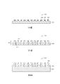
研磨墊圖案
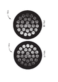
第14A-14O圖為依據本揭示之實施例的研磨墊設計之示意圖。第14A-14O圖的每個圖都包括像素圖,像素圖具有表示用於接觸和研磨基板的研磨特徵1402a-1402o的白色區域(在白色像素的區域)及表示基部特徵1404a-1404o的黑色區域(在黑色像素的區域)。研磨特徵1402a-1402o可以類似於研磨墊200的硬特徵204。基部特徵1404a-1404o可以類似於研磨墊200的彈性特徵206。白色區域通常突出於黑色區域上方,使得通道被形成在黑色區域中介於白色區域之間。在研磨過程中,研磨漿可以流過通道而且可以被保留在通道中。第14A-14O圖中圖示的研磨墊可以藉由使用3D列印機沉積複數個材料層來形成。該複數個層的每個層皆可包括兩種或更多種材料,以形成研磨特徵1402a-1404o和基部特徵1404a-1404o。在一個實施例中,在垂直於平行該複數個材料層的平面的方向上,研磨特徵1402a-1402o可以比基部特徵1404a-1404o更厚,使得凹槽及/或通道被形成在研磨墊的頂表面上。Figures 14A-14O are schematic diagrams of polishing pad designs according to embodiments of the present disclosure. Each of Figures 14A-14O includes a pixel map with white areas (in areas of white pixels) representing grinding
第14A圖為具有複數個同心研磨特徵1402a的研磨墊設計1400a之示意性像素圖。研磨特徵1402a可以是具有相同寬度的同心圓。在一個實施例中,基部特徵1404a也可以具有相同的寬度,使得研磨特徵1402a沿徑向方向的間距是固定的。在研磨過程中,研磨特徵1402a之間的通道保留研磨漿,並防止研磨漿因為研磨墊圍繞其中央軸(即同心圓的中心)旋轉所產生的離心力而快速損耗。Figure 14A is a schematic pixel diagram of a
第14B圖為具有複數個排列成同心圓的分段研磨特徵1402b的研磨墊設計1400b之示意性像素圖。在一個實施例中,分段的研磨特徵1402b可以具有大致上相同的長度。分段的研磨特徵1402b可以形成複數個同心圓。在每個圓中,分段的研磨特徵1402b可以被平均地分配在每個同心圓內。在一個實施例中,分段的研磨特徵1402b可以在徑向方向上具有相同的寬度。在一些實施例中,分段的研磨特徵1402b每個大致具有相同的長度而與同心圓的半徑無關(例如相等的弧長,除了研磨墊的中心區域之外)。在一個實施例中,該複數個同心圓之間的基部特徵1404b也可以具有相同的寬度,使得同心圓的間距是固定的。在一個實施例中,分段的研磨特徵1402b之間的間隙可以在圓和圓之間交錯,以防止研磨漿在研磨墊圍繞其中央軸旋轉所產生的離心力之下直接從研磨墊流出。14B is a schematic pixel diagram of a
第14C圖為具有複數個被形成在基部特徵1404c上方的同心研磨特徵1402c的研磨墊設計1400c之示意性像素圖。第14C圖的墊設計類似於第14A圖的墊設計1400a,不同之處僅在於研磨特徵1402c的寬度沿著徑向方向逐漸改變。在一個實施例中,研磨特徵的寬度從研磨墊的中心往研磨墊的邊緣減小,而相鄰的研磨特徵1402c之間的距離保持固定。在研磨墊圍繞中心軸旋轉時,研磨特徵1402c的寬度變化可被用來補償被研磨的基板在研磨墊的各個徑向位置的線性速度之差異。Figure 14C is a schematic pixel diagram of a
第14D圖為具有複數個被形成在基部特徵1404d上方的同心研磨特徵1402d的研磨墊設計1400d之示意性像素圖。第14D圖的墊設計類似於第14A圖的墊設計1400a,不同之處僅在於研磨特徵1402d是橢圓形而不是圓形。橢圓形研磨特徵1402d將允許研磨墊上的任何徑向位置具有多種尺寸和方向的研磨特徵,從而提高研磨均勻度。Figure 14D is a schematic pixel diagram of a
第14E圖為具有複數個被形成在基部特徵1404e上方的同心橢圓研磨特徵1402e的研磨墊設計1400e之示意性像素圖。第14E圖的墊設計類似於第14D圖的墊設計1400d,不同之處僅在於橢圓研磨特徵1402e沿著徑向方向改變寬度。具有不同寬度的橢圓研磨特徵將允許研磨墊上的徑向位置在研磨過程中接觸基板的研磨特徵中具有更多的變化,從而提高研磨均勻度。Figure 14E is a schematic pixel diagram of a
第14F圖為在基部特徵1404f上方具有螺旋研磨特徵1402f的研磨墊設計1400f之示意性像素圖。在第14F圖中,研磨墊1400f具有四個從研磨墊中心延伸到研磨墊邊緣的螺旋研磨特徵1402f。即使圖示出四個螺旋研磨特徵,但可以以類似的方式配置數量更少或更多的螺旋研磨特徵1402f。螺旋研磨特徵1402f界定螺旋通道。在一個實施例中,每個螺旋研磨特徵1402f具有固定的寬度。在一個實施例中,螺旋通道還具有固定的寬度。在研磨過程中,研磨墊可以圍繞中央軸以與螺旋研磨特徵1402f的方向相反的方向旋轉,以將研磨漿保留在螺旋通道中。例如,在第14F圖中,螺旋研磨特徵1402f和螺旋通道被形成為逆時針的方向,因此在研磨過程中,研磨墊可以以順時針方向旋轉,以將研磨漿保留在螺旋通道中和在研磨墊上。在一些配置中,每個螺旋通道從研磨墊中心到研磨墊邊緣是連續的。這個連續的螺旋通道允許研磨漿連同任何研磨廢料從研磨墊中心流到研磨墊邊緣。在一個實施例中,研磨墊可以藉由以與螺旋研磨特徵1402f相同的方向(例如在第14F圖的逆時針方向)旋轉研磨墊進行清洗。Figure 14F is a schematic pixel diagram of a
第14G圖為具有被以螺旋圖案配置在基部特徵1404g上的分段研磨特徵1402g的研磨墊設計1400g之示意性像素圖。第14G圖的研磨墊類似於第14F圖的研磨墊,不同之處僅在於螺旋研磨特徵1402g被分段。在一個實施例中,分段的研磨特徵1402g大致上具有相同的長度。分段的研磨特徵1402g可以沿著每個螺旋研磨特徵平均分佈。在一些實施例中,分段的研磨特徵1402g可以在螺旋方向上各自具有大致上相同的長度。Figure 14G is a schematic pixel diagram of a
第14H圖為具有被以螺旋圖案配置在基部特徵1404h上的分段研磨特徵1402h的研磨墊設計1400h之示意性像素圖。第14H圖的研磨墊類似於第14G圖的研磨墊,不同之處僅在於分段的研磨特徵1402h長度改變。在一個實施例中,分段研磨特徵1402h的長度從研磨墊的中心增加到研磨墊的邊緣區。Figure 14H is a schematic pixel diagram of a
第14I圖為具有被以螺旋圖案配置在基部特徵1404i上的分段研磨特徵1402i的研磨墊設計1400i之示意性像素圖。第14I圖的研磨墊類似於第14G圖的研磨墊,不同之處僅在於分段研磨特徵1402i的徑向間距改變。在一個實施例中,分段研磨特徵1402i的徑向間距從研磨墊的中心減小到研磨墊的邊緣區。Figure 14I is a schematic pixel diagram of a
第14J圖為具有被以螺旋圖案配置在基部特徵1404j上的分段研磨特徵1402j的研磨墊設計1400j之示意性像素圖。第14J圖的研磨墊類似於第14I圖的研磨墊,不同之處僅在於分段研磨特徵1402j的徑向間距從研磨墊的中心增加到研磨墊的邊緣區。Figure 14J is a schematic pixel diagram of a
第14K圖為具有複數個被形成在基部特徵1404k中的個別研磨特徵1402k的研磨墊設計1400k之示意性像素圖。在一個實施例中,複數個研磨特徵1402k的每一個都可以是圓柱。在一個實施例中,複數個研磨特徵1402k可以在研磨表面的平面中具有相同的尺寸。在一個實施例中,複數個圓柱形研磨特徵1402k可以被配置成同心圓。在一個實施例中,複數個圓柱形研磨特徵1402k可以被相對於研磨表面的平面配置成規則的2D圖案。Figure 14K is a schematic pixel diagram of a
第14L圖為具有複數個被形成在基部特徵1404l上方的個別研磨特徵1402l的研磨墊設計1400l之示意性像素圖。第14L圖的研磨墊類似於第14K圖的研磨墊,不同之處僅在於第14L圖的每個個別研磨特徵1402l可以是中空的圓柱,或相對於研磨表面在其中形成有凹陷。中空圓柱允許一些研磨漿被保留在其中。Figure 14L is a schematic pixel diagram of a polishing pad design 1400l having a plurality of individual polishing features 1402l formed over base features 1404l. The polishing pad of FIG. 14L is similar to the polishing pad of FIG. 14K, except that each
第14M圖為具有複數個被形成在基部特徵1404m上方的個別研磨特徵1402m的研磨墊設計1400m之示意性像素圖。第14M圖的研磨墊類似於第14K圖的研磨墊,不同之處僅在於第14M圖的一些研磨特徵1402m可以被連接而形成一個或更多個封閉圓圈。該一個或更多個封閉圓圈可以形成一個或更多個在研磨過程中保留研磨漿的屏障。Figure 14M is a schematic pixel diagram of a
第14N圖為具有複數個被形成在基部特徵1404n中的個別研磨特徵1402n的研磨墊設計1400n之示意性像素圖。第14N圖的研磨墊類似於第14M圖的研磨墊,不同之處僅在於第14N圖的一些研磨特徵1402n可以被連接而形成一個或更多個螺旋鏈。該一個或更多個螺旋鏈可以引導研磨漿的流體流動,以幫助保留研磨漿和清洗研磨墊。Figure 14N is a schematic pixel diagram of a
第14O圖為具有複數個個別研磨特徵1402o和基部特徵1404o的研磨墊設計1400o之示意性像素圖。第14O圖的研磨墊類似於第14K圖的研磨墊,不同之處僅在於第14O圖的每個個別研磨特徵1402o具有應用材料公司的標誌的形狀。第14O圖說明的是,本揭示的實施例涵括的研磨墊具有有任何適當設計、圖案及/或配置的研磨特徵。Figure 140 is a schematic pixel diagram of a polishing pad design 1400o having a plurality of individual polishing features 1402o and base features 1404o. The polishing pad of Figure 14O is similar to the polishing pad of Figure 14K, except that each individual polishing feature 1402o of Figure 14O has the shape of the Applied Materials logo. 140 illustrates that embodiments of the present disclosure encompass polishing pads having polishing features of any suitable design, pattern, and/or configuration.
第14A-14O圖的設計中的研磨特徵1402a-1402o可以由相同的材料或相同的材料組成物形成。或者,第14A-14O圖的設計中的研磨特徵1402a-1402o之材料組成物及/或材料性質可以隨著研磨特徵而改變。個別化的材料組成物及/或材料性質允許研磨墊可以依據特定需求來訂製。The
當研磨特徵是由兩種不同的3D列印材料形成時,研磨特徵可以藉由使用兩個列印頭列印至少兩個重疊的影像來製造。第15A-15B圖至第18A-18B圖提供具有複合研磨特徵的研磨墊之設計實例。在第15-18圖中,白色像素標記是材料液滴分配之處,而黑色像素標記在一個或更多個用以形成研磨墊的層內沒有分配材料之處。藉由使用這些技術,可以在一個或更多個用以形成完整的研磨墊之至少一部分的列印層中形成材料組成物中的梯度。可以使用研磨墊內的一個或更多個列印層之訂製組成物來調整和訂製研磨墊的整體機械性質。When the abrasive features are formed from two different 3D printing materials, the abrasive features can be fabricated by printing at least two overlapping images using two print heads. Figures 15A-15B through 18A-18B provide design examples of polishing pads with composite polishing features. In Figures 15-18, white pixels mark where droplets of material are dispensed, while black pixels mark where no material is dispensed within one or more of the layers used to form the polishing pad. Using these techniques, gradients in material composition can be formed in one or more of the printed layers used to form at least a portion of a complete polishing pad. The overall mechanical properties of the polishing pad can be adjusted and customized using custom compositions of one or more printed layers within the polishing pad.
藉由使用這些技術,在一些實施例中,理想的是在垂直於研磨墊之研磨表面的方向(例如垂直於第15-18圖圖示的圖之方向)上或在研磨墊之研磨表面的平面中(例如徑向方向)在材料組成物中形成梯度。在一個實施例中,理想的是在上面討論的硬及/或彈性特徵中、在垂直於研磨墊之研磨表面的方向上、在材料組成物中形成梯度。在一個實例中,理想的是在靠近研磨墊基部(例如與研磨表面相對)的列印層中具有較高濃度的、用以形成彈性特徵的材料,並且在靠近研磨墊之研磨表面的列印層中具有較高濃度的、用以形成硬特徵的材料。在另一個實例中,理想的是在靠近研磨墊基部的列印層中具有較高濃度的、用以形成硬特徵的材料,並且在靠近研磨墊之研磨表面的列印層中具有較高濃度的、用以形成彈性特徵的材料。By using these techniques, in some embodiments, it is desirable to be in a direction perpendicular to the polishing surface of the polishing pad (eg, perpendicular to the direction of the diagrams illustrated in Figures 15-18) or in the direction of the polishing surface of the polishing pad. A gradient is formed in the material composition in a plane (eg radial direction). In one embodiment, it is desirable to form a gradient in the material composition in a direction normal to the polishing surface of the polishing pad in the hard and/or elastic features discussed above. In one example, it is desirable to have a higher concentration of the material used to form the elastic features in the print layer near the base of the polishing pad (eg, opposite the polishing surface), and in the print near the polishing surface of the polishing pad A layer with a higher concentration of material used to form hard features. In another example, it is desirable to have a higher concentration of the material used to form the hard features in the print layer near the base of the polishing pad, and a higher concentration in the print layer near the polishing surface of the polishing pad materials used to form elastic characteristics.
堆疊的3D列印層的材料組成物及/或材料性質中的梯度可以在一個方向上從高濃度變化到低濃度,或反之亦然。在一些情況下,一個或更多個具有研磨墊的區域可以包括更複雜的濃度梯度,例如高/低/高或低/高/低的濃度梯度。在一種配置中,濃度梯度可以藉由改變所形成的研磨墊之每個連續層中第一列印成分對第二列印成分的位置及/或量來形成。例如,第一層可以具有1:1的第一列印成分對第二列印成分比率,在第二層中具有2:1的第一列印成分對第二列印成分比率,以及在第三層中具有3:1的第一列印成分對第二列印成分比率。也可以藉由調整列印液滴在沉積層平面內的配置而在單一層的不同部分內形成梯度。The gradient in the material composition and/or material properties of the stacked 3D printed layers may vary in one direction from high concentration to low concentration, or vice versa. In some cases, one or more of the regions with the polishing pad may include more complex concentration gradients, such as high/low/high or low/high/low concentration gradients. In one configuration, a concentration gradient can be created by varying the location and/or amount of the first printed component versus the second printed component in each successive layer of the polishing pad formed. For example, the first layer may have a 1:1 ratio of the first print component to the second print component, a 2:1 ratio of the first print component to the second print component in the second layer, and a 2:1 ratio of the first print component to the second print component in the second layer. The three layers have a 3:1 ratio of the first print component to the second print component. Gradients can also be created in different parts of a single layer by adjusting the placement of the print droplets in the plane of the deposited layer.
第15A圖和第15B圖為照出具有複合特徵的研磨墊之像素圖的黑白位圖影像。在第15A圖、第15B圖中,白色像素標記是分配材料液滴之處,而黑色像素標記沒有分配材料之處。第15A圖是用於研磨墊的第一材料之像素圖1500a,而第15B圖是用於相同研磨墊的第二材料之像素圖1500b。第一材料可以依照像素圖1500a藉由第一列印頭分配,而第二材料可以依照像素圖1500b藉由第二列印頭分配。這兩個列印頭將像素圖1500a、1500b重疊在一起而形成複數個個別的研磨特徵。靠近研磨墊邊緣區的研磨特徵包括比第二材料多的第一材料。靠近研磨墊中心區的研磨特徵包括比第一材料多的第二材料。在本實例中,每個研磨特徵都具有獨特的、第一材料和第二材料的組成物。Figures 15A and 15B are black and white bitmap images showing pixel maps of a polishing pad with composite features. In Figures 15A, 15B, the white pixels mark where the droplets of material are dispensed, and the black pixels mark where no material is dispensed. Figure 15A is a pixel map 1500a of a first material for a polishing pad, and Figure 15B is a
第16A圖和第16B圖為具有複合特徵的研磨墊之示意性像素圖1600a、1600b。第16A圖是用於研磨墊的第一材料之像素圖1600a,而第16B圖是用於相同研磨墊的第二材料之像素圖1600b。依照第16A圖、第16B圖的研磨墊類似於第15A圖、第15B圖的研磨墊,不同之處僅在於第16A圖、第16B圖的研磨特徵較大。Figures 16A and 16B are
第17A圖和第17B圖為具有複合特徵的研磨墊之示意性像素圖1700a、1700b。第17A圖是用於研磨墊的第一材料之像素圖1700a,而第17B圖是用於相同研磨墊的第二材料之像素圖1700b。依照第17A圖、第17B圖的研磨墊類似於第15A圖、第15B圖的研磨墊,不同之處僅在於研磨特徵的成分橫跨研磨墊從左邊變化到右邊。Figures 17A and 17B are
第18A圖和第18B圖為具有複合特徵的研磨墊之示意性像素圖1800a、1800b。第18A圖是用於研磨墊的第一材料之像素圖1800a,而第18B圖是用於相同研磨墊的第二材料之像素圖1800b。依照第18A圖、第18B圖的研磨墊類似於第17A圖、第17B圖的研磨墊,不同之處僅在於第17A圖、第17B圖的研磨特徵較大。Figures 18A and 18B are
應當注意的是,研磨特徵的成分可以在任何適當的圖案中改變。雖然上述的研磨墊被圖示為由兩種材料形成,但包括三種或更多種特徵的複合研磨墊也在本揭示的範圍內。It should be noted that the composition of the abrasive features may vary in any suitable pattern. Although the polishing pads described above are illustrated as being formed of two materials, composite polishing pads that include three or more features are also within the scope of the present disclosure.
應當注意的是,在任何研磨墊設計(例如第14A-14O圖的研磨墊)中的研磨特徵之成分可以以與第15-18圖的研磨墊類似的方式改變。 積層製造和硬化技術 It should be noted that the composition of the polishing features in any polishing pad design (eg, the polishing pads of Figures 14A-14O) may vary in a similar manner to the polishing pads of Figures 15-18. Laminate manufacturing and hardening technology
第19圖繪示具有被定位在平臺組件1911上方的承載頭組件1900的例示性CMP站1902之剖視圖。承載頭組件1900通常包含耦接到承載頭1921的驅動系統1901。驅動系統1901可以被耦接到控制器(未圖示),控制器提供訊號給驅動系統1901,用於控制承載頭1921的旋轉速度和方向。驅動系統1901通常至少對承載頭1921提供旋轉運動,而且還可以被朝向平臺組件1911致動,使得在處理過程中,被保持在承載頭1921的基板1914之特徵1904側可以被對著CMP站1902的襯墊組件1913之處理表面1925放置。典型情況下,基板1914和處理襯墊組件1913被相對於彼此轉動,以從基板1914的特徵側1904去除材料。視製程參數而定,承載頭1921被以大於、小於、或等於平臺組件1911之旋轉速度的旋轉速度轉動。承載頭組件1900也能夠保持固定,而且在處理期間可以在一個路徑上移動。在處理期間,承載頭組件1900還可以提供橫跨襯墊組件1913之處理表面1925的軌道運動或掃動。襯墊組件1913可適於使用黏著層1906可釋放地結合到平臺組件1911的上表面。襯墊組件1913通常包括處理表面1925、黏著層1906,而且可以包括可選的背托層1907。19 shows a cross-sectional view of an
平臺組件1911被轉動地設置在基座1908上,而且通常被軸承1938支撐在基座1908上,使得平臺組件1911可以被相對於基座1908轉動。平臺組件1911可以由剛性材料製造,例如金屬或剛性塑料,而且在一個實施例中,平臺組件1911具有由介電質材料(例如CPVC)製造或使用介電質材料塗佈的上表面。平臺組件1911可以具有圓形、矩形或其他的平面形狀。
可以從研磨流體源1948通過適當的配管和控制提供研磨流體到被定位在CMP站1902之處理襯墊組件1913上方的噴嘴1917。在第19圖圖示的實施例中,研磨流體1941是由噴嘴1917提供。研磨流體1941可以被平臺端緣1958圍阻。研磨流體1941可以是去離子水(DIW)或其他主要由水(例如DIW)組成的研磨流體、或是在DIW中夾帶有研磨顆粒的漿液。Abrasive fluid may be provided from an
襯墊組件1913的處理表面1925可以進一步包括形成在處理表面1925之上表面上的圖案化表面1951,以便利基板1914的研磨。圖案化表面1951的圖案可以包括複數個延伸於處理表面1925上方的小突出物。該等突出物可以採用任何幾何形狀,例如橢圓形、圓形、矩形、六邊形、八邊形、三角形、或上述形狀之組合,而且可以如本文所述藉由三維列印製程形成。圖案化表面1951可以使用被定位來與襯墊組件1913的處理表面1925互動的調理裝置1955維護及/或更新。在一個實施例中,調理裝置1955包含電磁能量源1959。在一個實施例中電磁能量源1959是雷射,並被用來朝向處理表面1925發射一個或更多個電磁能量束1960。一個或更多個電磁能量束1960被用來選擇性地加熱及/或剝離處理表面1925的多個區域,以更新或維護處理表面1925上的圖案化表面1951。在一些實施例中,電磁能量源1959可被用來藉由選擇性加熱處理表面1925的個別區域而調理襯墊組件1913的處理表面1925。The
第20A圖為用於製備可被用在平臺組件上的襯墊組件的襯墊製造系統2000A之一個實施例的示意性等角視圖,該襯墊組件例如第19圖的平臺組件1911中使用的襯墊組件1913。在一個實施例中,襯墊製造系統2000A通常包括進料區段2002、列印區段2004及硬化區段2006。襯墊製造系統2000A被用來生產複數個列印墊2008,列印墊2008可被用作第19圖的平臺組件1911中的襯墊組件1913。雖然未圖示出,但襯墊製造系統2000A也可以被修改來列印輥對輥研磨系統中使用的襯墊。Figure 20A is a schematic isometric view of one embodiment of a
襯墊製造系統2000A還包括輸送帶2010,輸送帶2010包括被配置在至少兩個輥2014之間的捲筒2012。一個或兩個輥2014可以被耦接到驅動馬達2015,驅動馬達2015在A指示的箭頭所繪示的方向上轉動輥2014及/或捲筒2012。進料區段2002、列印區段2004及硬化區段2006可以被操作地耦接到控制器2011。輸送帶2010可以被控制器2011操作以連續或間歇地移動。The
進料區段2002可以包括供應輥2016,供應輥2016操作地耦接到輸送帶2010,供應輥2016可以是背托材料2017,這樣的聚合物材料,例如雙軸方向的聚對苯二甲酸乙二酯(BoPET)材料。供應輥2016可以被配置在進料輥2018上,進料輥2018被運動控制裝置2020驅動或控制。運動控制裝置2020可以是馬達及/或包括在供應輥2016上提供預定張力的制動系統,使得供應輥2016的展開速度是由驅動馬達2015及/或捲筒2012驅動。進料區段2002還可以包括前處理裝置2022。在列印區段2004列印之前,前處理裝置2022可設以噴灑或以其他方式提供塗層到背托材料2017上。在一些實施例中,在列印區段2004列印之前,前處理裝置2022可被用於加熱背托材料2017。The
列印區段2004包括被設置在進料區段2002下游的3D列印站2024。列印區段2004利用一個或更多個列印頭2027提供圖案化表面2028到背托材料2017上。列印區段2004可以包括耦接到運動控制裝置2032的可移動平台2030,運動控制裝置2032可被用於相對於背托材料2017和捲筒2012移動列印頭2027。The
列印頭2027可以被耦接到具有列印材料的材料源2025,列印材料可被用來形成圖案化表面2028。列印材料可以包括聚合材料,例如聚氨甲酸乙酯、聚碳酸酯、氟聚合物、PTFE、PTFA、聚伸苯硫(PPS)、或上述聚合材料之組合。實例還包括聚乙烯醇、果膠、聚乙烯吡咯啶酮、羥乙基纖維素、甲基纖維素、氫丙基甲基纖維素、羧甲基纖維素、羥丙基纖維素、聚丙烯酸、聚丙烯醯胺、聚乙二醇、聚羥基醚丙烯酸酯、澱粉、馬來酸共聚物、聚氧化乙烯、聚氨甲酸乙酯及上述之組合、或任何上述的其他材料。The
在一個實施例中,聚合材料可以被沉積為背托材料2017上的基料。所形成的聚合材料可以包含開孔或閉孔的聚氨甲酸乙酯材料,而且可以包括散佈在其中的奈米級顆粒。該等顆粒可以包括有機奈米顆粒。在一個實施例中,奈米顆粒可以包括分子或元素環及/或奈米結構。實例包括碳(C)的同素異形體,例如奈米碳管和其他結構、具有5鍵(五邊形)、6鍵(六邊形)、或超過6鍵的分子碳環。其他實例包括富勒烯狀超分子。在另一個實施例中,奈米級顆粒可以是陶瓷材料、氧化鋁、玻璃(例如二氧化矽(SiO
2))、及上述材料之組合或衍生物。在另一個實施例中,奈米級顆粒可以包括金屬氧化物,例如氧化鈦(IV)或二氧化鈦(TiO
2)、氧化鋯(IV)或二氧化鋯(ZrO
2)、上述材料之組合及上述材料之衍生物、以及其他氧化物。
In one embodiment, the polymeric material can be deposited as a binder on the
由列印頭2027形成的圖案化表面2028可以包含複合基材,例如聚合基質,該聚合基質可以由氨甲酸乙酯、三聚氰胺、聚酯、聚碸、聚乙酸乙烯酯、氟化烴等等、以及上述之混合物、共聚物及移植物所形成。在一個實施例中,聚合基質包含可由聚醚類液體氨甲酸乙酯形成的氨甲酸乙酯聚合物。液體氨甲酸乙酯可以與多官能胺、二胺、三胺或多官能性羥基化合物或混合官能性化合物反應,例如氨甲酸乙酯/脲交聯組成物中的羥基/胺,氨甲酸乙酯/脲交聯組成物在硬化時形成脲鏈接和交聯的聚合物網絡。The patterned
硬化區段2006包括可以被設置在殼體2034中或上的硬化裝置2033。殼體2034被設置在捲筒2012上方,使得捲筒2012和背托材料2017上的圖案化表面2028可以從殼體2034下方通過。硬化裝置2033可以是熱烘箱、紫外(UV)光發射器、或上述之組合。在一個實施例中,硬化裝置2033可以包括雷射光源2036和電子束發射器2038中之一者或兩者,雷射光源2036和電子束發射器2038可被用於硬化列印頭2027沉積的材料以形成圖案化表面2028。在一些實施例中,當使用電子束發射器時,襯墊製造系統2000A可以位在壓力可受控制的外殼中。雷射光源2036和電子束發射器2038可被單獨使用或與熱或UV能量組合使用。在一些實施例中,雷射光源2036和電子束發射器2038可被用於針對圖案化表面2028之特定部分的點硬化製程。由雷射光源2036或電子束發射器2038針對的點可以加熱圖案化表面2028的個別區域,以形成可比周邊部分更硬或較不可壓縮的個別區域表面。雷射光源2036也可被用於剝離部分的圖案化表面2028,以在圖案化表面2028上形成細微的紋理。
第20B圖為襯墊製造系統2000B的另一個實施例之示意性側視圖。襯墊製造系統2000B可以類似於第20A圖的襯墊製造系統2000A包括具有進料區段2002、列印區段2004及硬化區段2006的輸送帶2010。襯墊製造系統2000B還可以包括捲繞區段2009,用於製造輥對輥系統中使用的研磨物件2029。捲繞區段2009包括捲取輥2040,可以將上面列印有圖案化表面2028的研磨物件2029捲繞在捲取輥2040上。捲取輥2040可以被從襯墊製造系統2000A中移出,以被用作輥對輥平臺組件中的供應輥2018。在製造過程中,捲取輥2040可以被耦接到運動控制裝置2042。運動控制裝置2042可以是馬達及/或包括控制捲取輥2040之捲繞速度的制動系統。在一些實施例中,襯墊製造系統2000B被用來列印複數個列印墊2008(圖示於第20A圖),列印墊2008可被用來作為第19圖的平臺組件1911中的襯墊組件1913。Figure 20B is a schematic side view of another embodiment of a
襯墊製造系統2000B包括供應輥2016,供應輥2016可控制地展開捲筒2012,捲筒2012在輸送帶2010上方移動到捲取輥2040。捲筒2012可以是類似於第20A圖描述的背托材料2017的背托材料。與第20A圖描述的襯墊製造系統2000A類似,捲筒2012以及輸送帶2010和捲取輥2040的移動可以由運動控制裝置和控制器控制,而且為了簡潔的緣故,在第20B圖省略相關的描述。The
襯墊製造系統2000B包括位於進料區段2002和列印區段2004之間的可選前處理區段2044。可以使用前處理區段2044來將黏著或釋放層形成在捲筒2012上。或者,可以在列印區段2004使用3D列印站2024形成黏著或釋放層。當使用前處理區段2044時,可以使用狹縫/模具塗佈機2046來沉積一個層或多個層到捲筒2012上。此外,可以使用利用紫外光或加熱元件的硬化站2048來硬化由狹縫/模具塗佈機2046沉積的材料。The
在此實施例中,3D列印站2024包含列印頭2026的陣列。列印頭2026可被用於可選地在捲筒2012上形成黏著或釋放層以及在捲筒2012上形成圖案化表面2028。在一個實例中,多列和多行的列印頭2026可以橫跨輸送帶2010的寬度和輸送帶2010的部分長度。在一些實施例中,一個或更多個列印頭2026可以相對於輸送帶2010移動。列印頭2026將可被耦接到材料源2025,如第20A圖所述。In this embodiment, the
硬化區段2006可以包括可選的電磁能量源2050和熱硬化裝置2052中之一者或兩者。電磁能量源2050可以是如第20A圖所述的雷射源或電子束發射器中之一者或組合。熱硬化裝置2052可以是烘箱或UV光陣列。
襯墊捲繞區段2009包括可以捲繞研磨物件2029的捲取輥2040。捲取輥2040可以被從襯墊製造系統2000A中移出,以被用作輥對輥平臺組件中的供應輥。The pad winding section 2009 includes a take-
第21A圖為可被用於第20A圖的襯墊製造系統2000A或第20B圖的襯墊製造系統2000B的3D列印站2024A之一個實施例的示意性剖視圖。第21A圖圖示使用3D列印製程製造的研磨墊2102之一個實施例的一部分。研磨墊2102可以是第19圖描述的襯墊組件1913、列印墊2008(圖示於第20A圖)、或研磨物件2029(圖示於第20B圖)。3D列印提供方便且高度可控的製程來生產在研磨層內的特定位置中內嵌有研磨料的研磨物件。研磨墊2102可以被列印在支座2100上,支座2100可以是第20A圖的背托材料2017或第20B圖的捲筒2012。Figure 21A is a schematic cross-sectional view of one embodiment of a
參照第21A圖,研磨墊2102的至少一個研磨層2105是使用3D列印製程製造的。在製造製程中,薄的材料層被逐步沉積和熔合在支座2100上,同時支座被沿著由A指示的箭頭(在X方向上)移動。例如,可以從液滴噴射列印機2115的噴嘴2126噴射出襯墊前驅物材料(來自第20A圖的材料源2025)的液滴2110,以形成複數個層2120A、2120B及2122。該等層可以形成包含襯墊前驅物材料的固化材料2125,使得能夠在固化材料2125上相繼沉積其他的層。液滴噴射列印機2115可以類似於噴墨列印機,但使用襯墊前驅物材料而不是油墨。在製造過程中,噴嘴2126可以在X和Y方向中的一個或兩個方向上平移,同時支座2100在X方向上連續或間歇地移動。Referring to FIG. 21A, at least one
在一個實例中,第一層2120A可以藉由噴射液滴2110到支座2100上來沉積。在固化之後可以將後續的層,例如層2120B和2122(為了簡潔起見未說出之間的其他層)沉積在第一層2120A上。在每一層被固化之後,新的層隨後被沉積在先前沉積的層上面,直到製造出完整的3維研磨層2105。固化可以藉由聚合來完成。例如,襯墊前驅物材料層可以是單體,而且該單體可以藉由UV硬化或熱原位聚合。襯墊前驅物材料可以在沉積後被立即有效地硬化,或是可以沉積整個襯墊前驅物材料層,然後可以同時硬化所有的沉積層。In one example, the
每個層都可以藉由噴嘴2126以儲存在3D繪圖電腦程式中的圖案施加,3D繪圖電腦程式被提供在控制器2111上。每個層2120A、2120B及2122都可以小於50 %的研磨層2105總厚度或小於研磨層2105的總厚度。在一個實例中,每個層2120A、2120B及2122都可以小於10 %的研磨層2105總厚度,例如小於5 %的研磨層2105總厚度,例如約小於1 %的研磨層2105總厚度。在一個實施例中,每個層的厚度可以包括約30微米至約60微米或更小的厚度,例如在奈米的量級上(例如1至100奈米),甚至到皮級的尺寸(例如10
−12米)。
Each layer can be applied by the
支座2100可以是剛性的基座或是撓性薄膜,例如聚四氟乙烯(PTFE)層。假使支座2100是薄膜,則支座2100可以可選地形成研磨墊2102的一部分。例如,支座2100可以是背托層2017或是在背托層2017和研磨層2105之間的層。或者,研磨層2105可以被從支座2100移除,並且層2120A和2120B可以形成背托層2017。The
在一些實施例中,研磨顆粒可以被分散在襯墊前驅物材料的液滴2110中。在形成每個層的過程中,研磨顆粒可以被局部分散到研磨層2105中。局部分散研磨顆粒可以有助於最少化結塊。在一些實施例中,研磨顆粒可以與液體熱固性聚合物前驅物預混。連續攪拌熱固性聚合物前驅物和研磨顆粒的混合物可防止顆粒結塊,類似用以均勻化噴墨印表機中使用的油墨顏料的設備。另外,連續攪拌混合物可確保研磨顆粒相當均勻地分散在前驅物材料中。這可導致顆粒在研磨層各處更均勻地分散,從而導致改良的研磨均勻性,也可以有助於避免結塊。In some embodiments, abrasive particles may be dispersed in
預混的混合物可以依據特定圖案被從單一噴嘴(例如噴嘴2126)分配。例如,預混的混合物可以被均勻地分配,以產生在整個研磨層2105的厚度具有均勻分佈的嵌入研磨顆粒的均勻研磨層2105。The premixed mixture can be dispensed from a single nozzle (eg, nozzle 2126) according to a particular pattern. For example, the premixed mixture can be uniformly distributed to produce a uniform
第21B圖為可用於第20A圖的襯墊製造系統2000A或第20B圖的襯墊製造系統2000B的3D列印站2024B之一個實施例的示意性剖視圖。第21B圖示使用3D列印製程製造的研磨墊2132之另一個實施例的一部分之剖視圖。研磨墊2132可以是第19圖描述的襯墊組件1913、列印墊2008(圖示於第20A圖)、或研磨物件2029(圖示於第20B圖)。Figure 21B is a schematic cross-sectional view of one embodiment of a
如第21B圖所圖示,研磨墊2132是依據來自CAD程式的指令藉由液滴噴射列印機2115形成為包括複數個被凹槽2155分離的結構2150。結構2150和凹槽2155可以形成研磨層2105。子層2130也可以藉由液滴噴射列印機2115使用研磨物件形成。子層2130可以是背托層2017(圖示於第20A圖)。例如,子層2130和研磨層2105可以藉由液滴噴射列印機2115以不中斷的操作製造。子層2130可以藉由使用不同的前驅物及/或不同的硬化量(例如不同的紫外線輻射強度或持續時間)而被提供與研磨層2105不同的硬度。在其他的實施例中,子層2130是藉由傳統的製程製造,然後被固定於研磨層2105。例如,研磨層2105可以藉由薄的黏著層(例如壓敏黏著劑)被固定於子層2130。As shown in FIG. 21B , the
在第21B圖中,可以使用具有噴嘴2135的列印頭2126A來分配純液體熱固性聚合物前驅物,而具有噴嘴2135的列印頭2126B可被用於液體熱固性聚合物前驅物或其中含有研磨顆粒2145的熔融熱塑性塑膠。研磨顆粒2145的液滴2140可以只被分配在研磨墊2132上的選定位置。這些選定位置共同形成研磨顆粒的目標列印圖案,而且可以被儲存為CAD相容檔案,然後該CAD相容檔案被控制液滴噴射列印機2115的電子控制器(例如控制器2111)讀取。然後電子控制訊號被發送到液滴噴射列印機2115,以只在噴嘴2135被平移到該CAD相容檔案指定的位置時分配預混的混合物。In Figure 21B, the
或者,取代使用液體熱固性聚合物前驅物的是,可以將研磨顆粒2145與熔融熱塑性塑膠預混。在本實施例中,具有研磨顆粒2145的混合物在被分配之前也被不斷攪拌。在依照目標列印圖案從液滴噴射列印機2115分配混合物之後,混合物的熔融部分冷卻並固化,並且研磨顆粒2145被原地凍結。連續攪拌混合物可確保研磨顆粒2145相當均勻地分佈在前驅物材料中。這可以導致顆粒2145更均勻地分佈在研磨層各處,從而可以改良研磨均勻性,也可以最少化結塊。Alternatively, instead of using a liquid thermoset polymer precursor, the
類似於使用液體熱固性聚合物前驅物的情況,可以均勻地分配熱塑性混合物,以在整個研磨層2105各處產生均勻分佈的研磨顆粒2145。或者,含有研磨顆粒的熱塑性混合物可以按照研磨顆粒2145的目標列印圖案只被分配在研磨層2105的選定位置,該目標列印圖案被儲存為CAD相容的檔案,並由用以驅動液滴噴射列印機2115的電子控制器讀取。Similar to the use of liquid thermoset polymer precursors, the thermoplastic mixture can be uniformly distributed to produce uniformly distributed
不是從耦接到列印頭2126B的噴嘴2135分配在懸浮液中的研磨顆粒,而是可以以粉末的形式從列印頭2126B的噴嘴2135直接分配研磨顆粒,同時使用列印頭2126A的噴嘴2135來分配襯墊聚合物前驅物。在一個實施例中,在將研磨顆粒2145分配到沉積的聚合物材料中之前分配聚合物前驅物,隨後並將該混合物硬化。Instead of dispensing abrasive particles in suspension from
雖然3D列印對於使用研磨顆粒2145(例如氧化鋁、二氧化鈰及其他將容易結塊者)建構研磨墊2132是特別有用的,但此作法亦可被用於分配其他的研磨顆粒。因此,研磨顆粒可以包括二氧化矽、陶瓷氧化物、金屬及硬聚合物。While 3D printing is particularly useful for constructing the
液滴噴射列印機2115可以沉積固體的顆粒2145或空心的顆粒2145。液滴噴射列印機2115也可以分配不同類型的顆粒,其中有一些類型的顆粒可以在CMP處理過程中進行化學反應,以在研磨墊2132的一個層或多個層上產生目標變化,以及與正被研磨的基板進行化學反應。CMP處理中使用的化學反應之實例包括在10-14的鹼性酸鹼度範圍內發生的、涉及氫氧化鉀、氫氧化銨中之一者或更多者的化學製程、及其他由漿料的製造商使用的專利化學製程。CMP處理中也使用在2-5的酸性酸鹼度範圍內發生的、涉及諸如乙酸、檸檬酸等有機酸的化學製程。涉及過氧化氫的氧化反應也是CMP處理中使用的化學反應之實例。研磨顆粒2145也可被用來提供機械研磨功能。顆粒2145可以具有高達1毫米、或更小例如10微米、或更小例如1微米、或更小的尺寸。顆粒2145可以具有不同的形態,例如顆粒2145可以是圓的、細長的或多刻面的。The
由於逐層列印的作法,3D列印作法允許在研磨層2105的圖案中實現嚴密的公差,並在被嵌入研磨層2105的研磨顆粒2145之分佈中實現高的公差。
研磨墊 The 3D printing approach allows tight tolerances in the pattern of the
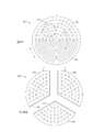
第22圖圖示研磨墊2200的一個實施例之一部分,研磨墊2200可被用作第19圖描述的襯墊組件1913、列印墊2008(圖示於第20A圖)、或研磨物件2029(圖示於第20B圖)。研磨墊2200包括形成第20A圖和第20B圖之圖案化表面2028的研磨表面2205。研磨表面2205包括複數個形成在研磨材料2270中的孔2232。研磨材料2270可以藉由適當的黏著劑2219結合於背托材料2222,選擇可抵抗CMP製程中使用的化學和物理元素的黏著劑2219。研磨墊2200中的孔2232大致上是圓形或橢圓形的形狀,但也可以包含其他的環狀幾何形狀,例如圓錐體或中空截頭錐體,即在大致上平行的平面之間的圓錐體。研磨墊2200也可以被形成為匹配第14A-14O圖中圖示的任何研磨墊設計或本文描述的其他設計。FIG. 22 illustrates a portion of one embodiment of a
在一個實施例中,孔2232可以是中空的(即空的空間),孔2232可被依尺寸製作及/或間隔開,以增進漿料保留並有助於研磨墊2200的旋轉。在其他實施例中,孔2232可被至少部分使用第一材料2210填充,第一材料2210與研磨材料2270(第二材料2212)不同。第一材料2210可以是與第二材料2212相比對硬化方法具有不同反應性的聚合物材料。例如,在一個實施例中,第二材料2212可以使用UV能量硬化,而第一材料2210並不明顯受到紫外線能量影響。然而,在一個實施例中,第一材料2210可以被熱硬化。在其他實施例中,第一材料2210和第二材料2212可被以不同速率硬化。在一個實施例中,研磨墊2200可使用第一材料2210和第二材料2212而被差別硬化。在一個差別硬化的實例中,研磨墊2200的第一材料2210和第二材料2212可以使用不硬化第一材料2210的UV能量硬化。這可以使第二材料2212比第一材料2210更硬,從而可以對研磨墊2200添加壓縮性及/或可撓性,因為第一材料2210比第二材料2212更黏稠。In one embodiment, the
在一個實施例中,第一材料2210被熱固化以使孔2232中配置有較硬的第一材料2210,但仍比第二材料2212更軟且更可壓縮。在另一個實施例中,孔2232中的第一材料2210是藉由基板研磨製程期間的摩擦所產生的熱熱硬化的。在本實施例中,第一材料2210可以被硬化成比第二材料2212更硬,從而在研磨表面2205上形成比周圍的第二材料2212更硬的區域。In one embodiment, the
在其他實施例中,當與第二材料2212相比時,第一材料2210可以具有不同的、與電磁能量的反應性,該電磁能量例如來自電磁能量源1959(圖示於第19圖)的一個能量束或多個能量束。可以利用不同的反應性在研磨表面2205上形成微紋理。第一材料2210和第二材料2212之間的不同反應性可以提供的是第一材料2210將被以比第二材料2212更快的速率剝離,或反之亦然。孔2232可以是在研磨墊2200的研磨表面2205內形成微米尺寸或奈米尺寸區域的微米尺寸或奈米尺寸材料。在一個實施例中,孔2232可以包括小於約150微米至約10微米、或更小的平均直徑。In other embodiments, the
本揭示的一個實施例提供一種包括複合襯墊主體的研磨墊。該複合襯墊主體包括一個或更多個由第一聚合物材料形成的第一特徵,以及一個或更多個由第二聚合物材料形成的第二特徵。該一個或更多個第一特徵和該一個或更多個第二特徵是藉由沉積複數個包含第一聚合物材料和第二聚合物材料的層所形成的。第一特徵或第二特徵其中一者被差別硬化,以在其間提供差別的硬度或其他有用的材料性質。在一個實施例中,該一個或更多個第一特徵和該一個或更多個第二特徵被交替配置在襯墊主體各處。在一個實施例中,該一個或更多個第一特徵比該一個或更多個第二特徵更厚,使得凹槽及/或通道被形成在複合襯墊主體的頂表面上。在一個實施例中,該一個或更多個第一特徵包含複數個被該一個或更多個第二特徵分隔的同心環。在一個實施例中,該一個或更多個第一特徵包含複數個被該一個或更多個第二特徵包圍的圓柱。在一個實施例中,該一個或更多個第一特徵和該一個或更多個第二特徵係藉由3D列印形成。在一個實施例中,研磨墊進一步包括兩個或更多個邊緣結合在一起的複合襯墊主體。在一個實施例中,研磨墊進一步包括子襯墊主體,其中複合襯墊主體被形成在該子襯墊主體上方。在一個實施例中,該一個或更多個第一特徵包含其中配置有第三材料的孔。第三材料是熱硬化的材料。在一個實施例中,該第一聚合物材料具有第一楊氏模數,並且該第二聚合物材料具有第二楊氏模數。在一個實施例中,該第一材料具有比該第二材料更高的彈性模數。One embodiment of the present disclosure provides a polishing pad including a composite pad body. The composite pad body includes one or more first features formed from a first polymeric material, and one or more second features formed from a second polymeric material. The one or more first features and the one or more second features are formed by depositing a plurality of layers comprising a first polymeric material and a second polymeric material. Either the first feature or the second feature is differentially hardened to provide differential hardness or other useful material properties therebetween. In one embodiment, the one or more first features and the one or more second features are alternately arranged throughout the pad body. In one embodiment, the one or more first features are thicker than the one or more second features such that grooves and/or channels are formed on the top surface of the composite liner body. In one embodiment, the one or more first features comprise a plurality of concentric rings separated by the one or more second features. In one embodiment, the one or more first features comprise a plurality of cylinders surrounded by the one or more second features. In one embodiment, the one or more first features and the one or more second features are formed by 3D printing. In one embodiment, the polishing pad further includes a composite pad body with two or more edges joined together. In one embodiment, the polishing pad further includes a sub-pad body, wherein the composite pad body is formed over the sub-pad body. In one embodiment, the one or more first features comprise holes in which the third material is disposed. The third material is a thermosetting material. In one embodiment, the first polymeric material has a first Young's modulus and the second polymeric material has a second Young's modulus. In one embodiment, the first material has a higher modulus of elasticity than the second material.
雖然本文所述的研磨墊形狀為圓形,但依據本揭示的研磨顆粒可以包括任何適當的形狀,例如設以在研磨過程中線性移動的研磨捲筒。Although the shape of the polishing pad described herein is circular, abrasive particles in accordance with the present disclosure may include any suitable shape, such as a polishing drum configured to move linearly during the polishing process.
雖然前述內容是針對本揭示的實施例,但可以在不偏離本揭示之基本範圍下設計出本揭示的其他和進一步實施例,而且本揭示之範圍係由隨後的申請專利範圍所決定。While the foregoing is directed to embodiments of the present disclosure, other and further embodiments of the present disclosure can be devised without departing from the essential scope of the present disclosure, which is determined by the scope of the claims that follow.
100:研磨站 102:平臺 104:中心軸 106:研磨墊 108:承載頭 110:基板 112:研磨表面 114:中心軸 116:研磨流體 118:輸送臂 200:研磨墊 200b:研磨墊 200c:研磨墊 200d:研磨墊 202:複合襯墊主體 204:硬特徵 204b:硬特徵 204c:硬特徵 204d:硬特徵 206:彈性特徵 206b:彈性特徵 206c:彈性特徵 206d:彈性特徵 208:上表面 210:高度 212:高度 214:寬度 216:間距 218:凹槽 220:垂直脊 222:垂直凹槽 224:側壁 225:凹陷側壁 226:水平脊 227:水平凹槽 300:研磨墊 300b:研磨墊 300c:研磨墊 302:表面特徵 302b:表面特徵 302c:表面特徵 304:基材層 304b:基材層 304c:基材層 306:上表面 310:垂直脊 312:垂直凹槽 314:水平脊 316:水平凹槽 400:研磨墊 402:基層 404:硬特徵 406:表面特徵 408:外表面 500:研磨墊 502:襯墊主體 504:硬特徵 506:彈性特徵 510:觀察窗 600:研磨墊 602:表面特徵 604:基材層 606:背托層 700:研磨墊 702:複合襯墊主體 704:背托層 706:外邊緣區域 708:中央區域 710:內邊緣區域 802:表面特徵 804:表面特徵 806:基材層 808:基材層 810:鎖定層 900:研磨墊 902:研磨表面 904:研磨表面 1000:研磨墊 1002:複合襯墊主體 1004:複合襯墊主體 1006:複合襯墊主體 1008:鎖定特徵 1010:鎖定特徵 1200:3D列印站 1202:支座 1204:電子控制器 1206:液滴噴射列印機 1208:列印頭 1210:噴嘴 1212:噴嘴 1214:列印頭 1300:研磨墊 1304a:硬特徵 1304b:硬特徵 1306:彈性特徵 1316:液滴 1318:液滴 1400a-1400o:研磨墊設計 1402a-1402o:研磨特徵 1404a-1404o:基部特徵 1500a:像素圖 1500b:像素圖 1600a:像素圖 1600b:像素圖 1700a:像素圖 1700b:像素圖 1800a:像素圖 1800b:像素圖 1900:承載頭組件 1901:驅動系統 1902:CMP站 1904:特徵 1906:黏著層 1907:背托層 1908:基座 1911:平臺組件 1913:襯墊組件 1914:基板 1917:噴嘴 1921:承載頭 1925:處理表面 1938:軸承 1941:研磨流體 1948:研磨流體源 1951:圖案化表面 1955:調理裝置 1958:平臺端緣 1959:電磁能量源 1960:電磁能量束 2000A:襯墊製造系統 2000B:襯墊製造系統 2002:進料區段 2004:列印區段 2006:硬化區段 2008:列印墊 2009:捲繞區段 2010:輸送帶 2011:控制器 2012:捲筒 2014:輥 2015:驅動馬達 2016:供應輥 2017:背托材料 2018:進料輥 2020:運動控制裝置 2022:前處理裝置 2024:3D列印站 2024A:3D列印站 2024B:3D列印站 2025:材料源 2026:列印頭 2027:列印頭 2028:圖案化表面 2029:研磨物件 2030:可移動平台 2032:運動控制裝置 2033:硬化裝置 2034:殼體 2036:雷射光源 2038:電子束發射器 2040:捲取輥 2042:運動控制裝置 2044:前處理區段 2046:狹縫/模具塗佈機 2048:硬化站 2050:電磁能量源 2052:熱硬化裝置 2100:支座 2102:研磨墊 2105:研磨層 2110:液滴 2111:控制器 2115:液滴噴射列印機 2120A:層 2120B:層 2122:層 2125:固化材料 2126:噴嘴 2126A:列印頭 2126B:列印頭 2130:子層 2132:研磨墊 2135:噴嘴 2140:液滴 2145:研磨顆粒 2150:結構 2155:凹槽 2200:研磨墊 2205:研磨表面 2210:第一材料 2212:第二材料 2219:黏著劑 2222:背托材料 2232:孔 2270:研磨材料21:基板 21,22:基板 21~22:基板 100: Grinding Station 102: Platform 104: Center shaft 106: Grinding pad 108: Bearing head 110: Substrate 112: Grinding the surface 114: Center shaft 116: Grinding fluid 118: Conveyor Arm 200: Grinding pad 200b: Grinding pad 200c: Grinding pad 200d: Grinding pad 202: Composite pad body 204: Hard Features 204b: Hard Features 204c: Hard Features 204d: Hard Features 206: Elastic Features 206b: Elastic Features 206c: Elastic Features 206d: Elastic Features 208: Upper surface 210: height 212: height 214:width 216: Spacing 218: Groove 220: Vertical Ridge 222: Vertical groove 224: Sidewall 225: Recessed Sidewall 226: Horizontal Ridge 227: Horizontal groove 300: Polishing pad 300b: Grinding pad 300c: Grinding pad 302: Surface Features 302b: Surface Features 302c: Surface Features 304: substrate layer 304b: substrate layer 304c: Substrate layer 306: Upper surface 310: Vertical Ridge 312: Vertical groove 314: Horizontal Ridge 316: Horizontal groove 400: Grinding pad 402: Grassroots 404: Hard Features 406: Surface Features 408: outer surface 500: Grinding pad 502: Pad body 504: Hard Features 506: Elastic Features 510: Observation window 600: Grinding pad 602: Surface Features 604: substrate layer 606: back support layer 700: Grinding pad 702: Composite pad body 704: back support layer 706: Outer edge area 708: Central Area 710: Inner edge area 802: Surface Features 804: Surface Features 806: substrate layer 808: Substrate layer 810: Lock Layer 900: Grinding pad 902: Grinding Surface 904: Grinding Surface 1000: polishing pad 1002: Composite pad body 1004: Composite pad body 1006: Composite pad body 1008: Lock Features 1010: Lock Features 1200: 3D Printing Station 1202: Support 1204: Electronic Controller 1206: Drop Jet Printer 1208:Print Head 1210: Nozzle 1212: Nozzle 1214: Print Head 1300: Grinding pad 1304a: Hard Features 1304b: Hard Features 1306: Elastic Features 1316: Droplets 1318: Droplets 1400a-1400o: Pad Design 1402a-1402o: Grinding Features 1404a-1404o: Basal features 1500a: Pixmap 1500b: Pixmap 1600a: Pixmap 1600b: Pixmap 1700a: Pixmap 1700b: Pixmap 1800a: Pixmap 1800b: Pixmap 1900: Bearing Head Assembly 1901: Drive Systems 1902: CMP Station 1904: Features 1906: Adhesive Layer 1907: Back support layer 1908: Pedestal 1911: Platform Components 1913: Pad assembly 1914: Substrate 1917: Nozzles 1921: Bearing Head 1925: Treated Surfaces 1938: Bearings 1941: Grinding Fluids 1948: Grinding Fluid Source 1951: Patterned Surfaces 1955: Conditioning device 1958: Platform Edge 1959: Electromagnetic energy source 1960: Electromagnetic energy beam 2000A: Pad Manufacturing System 2000B: Pad Manufacturing System 2002: Feed Section 2004: Print section 2006: Hardened Section 2008: Printing Pad 2009: Winding Section 2010: Conveyor Belts 2011: Controller 2012: Reel 2014: Roll 2015: Drive Motor 2016: Supply Roll 2017: Back support material 2018: Feed Roller 2020: Motion Controls 2022: Pretreatment unit 2024: 3D Printing Station 2024A: 3D Printing Station 2024B: 3D Printing Station 2025: Material Sources 2026: Print Heads 2027: Printheads 2028: Patterned Surfaces 2029: Grinding Objects 2030: Movable Platforms 2032: Motion Control Devices 2033: Hardening Device 2034: Shell 2036: Laser light source 2038: Electron Beam Emitters 2040: Coil Roller 2042: Motion Control Devices 2044: Preprocessing section 2046: Slot/die coater 2048: Hardening Station 2050: Electromagnetic Energy Sources 2052: Thermosetting device 2100: Support 2102: Polishing Pad 2105: Abrasive layer 2110: Droplets 2111: Controller 2115: Drop Jet Printer 2120A: Layer 2120B: Layer 2122: Layer 2125: Cured Materials 2126: Nozzle 2126A: Print Head 2126B: Print Head 2130: Sublayer 2132: Grinding pad 2135: Nozzle 2140: Droplets 2145: Abrasive particles 2150: Structure 2155: Groove 2200: Grinding pad 2205: Grinding Surface 2210: First Material 2212: Second Material 2219: Adhesive 2222: Back support material 2232: Hole 2270: Abrasives 21: Substrates 21,22: Substrate 21~22: Substrate
為詳細瞭解上述本揭示之特徵,可參照實施例(其中一些圖示於附圖中)而對以上簡要概述的本揭示作更特定的描述。然而,應注意的是,附圖僅圖示本揭示之典型實施例,因此不應將該等附圖視為限制本揭示之範圍,因本揭示可認可其他等同有效的實施例。In order to understand in detail the features of the present disclosure described above, the present disclosure, briefly summarized above, may be described more particularly with reference to embodiments, some of which are illustrated in the accompanying drawings. It is to be noted, however, that the appended drawings illustrate only typical embodiments of the present disclosure and are therefore not to be considered limiting of its scope, for the present disclosure may admit to other equally effective embodiments.
第1圖為研磨站之示意性剖視圖。Figure 1 is a schematic cross-sectional view of a grinding station.
第2A圖為依據本揭示之一實施例的研磨墊之示意性立體剖視圖。FIG. 2A is a schematic perspective cross-sectional view of a polishing pad according to an embodiment of the present disclosure.
第2B圖為依據本揭示之一實施例的研磨墊之示意性局部俯視圖。FIG. 2B is a schematic partial top view of a polishing pad according to an embodiment of the present disclosure.
第2C圖為依據本揭示之一實施例的研磨墊之示意性局部剖視圖。FIG. 2C is a schematic partial cross-sectional view of a polishing pad according to an embodiment of the present disclosure.
第2D圖為依據本揭示之一實施例的研磨墊之示意性局部剖視圖。2D is a schematic partial cross-sectional view of a polishing pad according to an embodiment of the present disclosure.
第3A圖為依據本揭示之一實施例的研磨墊之示意性立體剖視圖。FIG. 3A is a schematic perspective cross-sectional view of a polishing pad according to an embodiment of the present disclosure.
第3B圖為依據本揭示之一實施例的研磨墊之示意性局部俯視圖。FIG. 3B is a schematic partial top view of a polishing pad according to an embodiment of the present disclosure.
第3C圖為依據本揭示之一實施例的研磨墊之示意性局部剖視圖。3C is a schematic partial cross-sectional view of a polishing pad according to an embodiment of the present disclosure.
第4圖為依據本揭示之一實施例的研磨墊之示意性立體剖視圖。FIG. 4 is a schematic perspective cross-sectional view of a polishing pad according to an embodiment of the present disclosure.
第5圖為依據本揭示之一實施例具有一個或更多個觀察窗的研磨墊之示意性立體剖視圖。5 is a schematic perspective cross-sectional view of a polishing pad having one or more viewing windows according to one embodiment of the present disclosure.
第6圖為依據本揭示之一實施例包括支撐泡沫層的研磨墊之示意性立體剖視圖。FIG. 6 is a schematic perspective cross-sectional view of a polishing pad including a support foam layer according to an embodiment of the present disclosure.
第7圖為依據本揭示之一實施例具有多個區域的研磨墊之示意性剖視圖。FIG. 7 is a schematic cross-sectional view of a polishing pad having multiple regions according to one embodiment of the present disclosure.
第8圖為依據本揭示之一實施例的第7圖研磨墊之局部放大剖視圖。FIG. 8 is a partial enlarged cross-sectional view of the polishing pad of FIG. 7 according to an embodiment of the present disclosure.
第9圖為依據本揭示之一實施例的研磨墊之示意性立體剖視圖。FIG. 9 is a schematic perspective cross-sectional view of a polishing pad according to an embodiment of the present disclosure.
第10圖為依據本揭示之一實施例的研磨墊之示意性立體剖視圖。FIG. 10 is a schematic perspective cross-sectional view of a polishing pad according to an embodiment of the present disclosure.
第11圖為第10圖的研磨墊之局部剖視圖。FIG. 11 is a partial cross-sectional view of the polishing pad of FIG. 10 .
第12圖為依據本揭示之一實施例用於製造研磨墊的設備之示意性剖視圖。12 is a schematic cross-sectional view of an apparatus for manufacturing a polishing pad according to an embodiment of the present disclosure.
第13圖為依據本揭示之一實施例具有從兩種材料的組成物形成的特徵的研磨墊之示意性局部剖視圖。13 is a schematic partial cross-sectional view of a polishing pad having features formed from a composition of two materials in accordance with one embodiment of the present disclosure.
第14A圖至第14O圖為依據本揭示之至少一個實施例的研磨墊設計之示意圖。14A to 14O are schematic diagrams of polishing pad designs according to at least one embodiment of the present disclosure.
第15A圖和第15B圖為依據本揭示之至少一個實施例具有複合特徵的研磨墊之示意圖。15A and 15B are schematic diagrams of a polishing pad having composite features according to at least one embodiment of the present disclosure.
第16A圖和第16B圖為依據本揭示之至少一個實施例具有複合特徵的研磨墊之示意圖。16A and 16B are schematic diagrams of a polishing pad having composite features according to at least one embodiment of the present disclosure.
第17A圖和第17B圖為依據本揭示之至少一個實施例具有複合特徵的研磨墊之示意圖。17A and 17B are schematic diagrams of a polishing pad having composite features according to at least one embodiment of the present disclosure.
第18A圖和第18B圖為依據本揭示之至少一個實施例具有複合特徵的研磨墊之示意圖。18A and 18B are schematic diagrams of a polishing pad having composite features according to at least one embodiment of the present disclosure.
第19圖為依據本揭示之一實施例的研磨站之示意性剖視圖。FIG. 19 is a schematic cross-sectional view of a grinding station according to an embodiment of the present disclosure.
第20A圖為依據本揭示之一實施例的研磨墊製造系統之示意性立體圖。FIG. 20A is a schematic perspective view of a polishing pad manufacturing system according to an embodiment of the present disclosure.
第20B圖為依據本揭示之另一個實施例的研磨墊製造系統之示意圖。FIG. 20B is a schematic diagram of a polishing pad manufacturing system according to another embodiment of the present disclosure.
第21A圖為依據本揭示之一實施例的3D列印站之示意圖。FIG. 21A is a schematic diagram of a 3D printing station according to an embodiment of the present disclosure.
第21B圖為依據本揭示之另一個實施例的3D列印站之示意圖。FIG. 21B is a schematic diagram of a 3D printing station according to another embodiment of the present disclosure.
第22圖為依據本揭示之一實施例的研磨墊之示意性立體圖。FIG. 22 is a schematic perspective view of a polishing pad according to an embodiment of the present disclosure.
為了便於理解,已在可能處使用共通的語詞來指稱對於圖式為共通的相同元件。構思的是,可以將在一個實施例中揭示的元件有益地用於其他實施例中而無需進一步詳述。To facilitate understanding, common terms have been used where possible to refer to the same elements that are common to the drawings. It is contemplated that elements disclosed in one embodiment may be beneficially utilized in other embodiments without further elaboration.
國內寄存資訊(請依寄存機構、日期、號碼順序註記) 無 國外寄存資訊(請依寄存國家、機構、日期、號碼順序註記) 無 Domestic storage information (please note in the order of storage institution, date and number) none Foreign deposit information (please note in the order of deposit country, institution, date and number) none
300:研磨墊 302:表面特徵 304:基材層 306:上表面 300: Polishing pad 302: Surface Features 304: substrate layer 306: Upper surface
Claims (20)
Applications Claiming Priority (6)
| Application Number | Priority Date | Filing Date | Title |
|---|---|---|---|
| US201462065193P | 2014-10-17 | 2014-10-17 | |
| US201462065270P | 2014-10-17 | 2014-10-17 | |
| US62/065,270 | 2014-10-17 | ||
| US62/065,193 | 2014-10-17 | ||
| US14/695,299 | 2015-04-24 | ||
| US14/695,299 US9873180B2 (en) | 2014-10-17 | 2015-04-24 | CMP pad construction with composite material properties using additive manufacturing processes |
Publications (2)
| Publication Number | Publication Date |
|---|---|
| TW202214386A TW202214386A (en) | 2022-04-16 |
| TWI775699B true TWI775699B (en) | 2022-08-21 |
Family
ID=55747459
Family Applications (8)
| Application Number | Title | Priority Date | Filing Date |
|---|---|---|---|
| TW104118517A TWI652141B (en) | 2014-10-17 | 2015-06-08 | Construction of CMP liners with composite properties using a laminate manufacturing process |
| TW111126883A TWI804387B (en) | 2014-10-17 | 2015-06-08 | Polishing pad and method of forming the same |
| TW108102209A TWI688451B (en) | 2014-10-17 | 2015-06-08 | Additive manufacturing system and method of forming a polishing pad |
| TW110148066A TWI775699B (en) | 2014-10-17 | 2015-06-08 | Polishing pad and method of forming the same |
| TW109112154A TWI753400B (en) | 2014-10-17 | 2015-06-08 | A polishing pad and a composite polishing pad |
| TW110117869A TW202146601A (en) | 2014-10-17 | 2015-10-19 | Precursor formulations for polishing pads produced by an additive manufacturing process |
| TW109103156A TWI730610B (en) | 2014-10-17 | 2015-10-19 | Precursor formulations for polishing pads produced by an additive manufacturing process |
| TW104134235A TWI687312B (en) | 2014-10-17 | 2015-10-19 | Polishing pads produced by an additive manufacturing process |
Family Applications Before (3)
| Application Number | Title | Priority Date | Filing Date |
|---|---|---|---|
| TW104118517A TWI652141B (en) | 2014-10-17 | 2015-06-08 | Construction of CMP liners with composite properties using a laminate manufacturing process |
| TW111126883A TWI804387B (en) | 2014-10-17 | 2015-06-08 | Polishing pad and method of forming the same |
| TW108102209A TWI688451B (en) | 2014-10-17 | 2015-06-08 | Additive manufacturing system and method of forming a polishing pad |
Family Applications After (4)
| Application Number | Title | Priority Date | Filing Date |
|---|---|---|---|
| TW109112154A TWI753400B (en) | 2014-10-17 | 2015-06-08 | A polishing pad and a composite polishing pad |
| TW110117869A TW202146601A (en) | 2014-10-17 | 2015-10-19 | Precursor formulations for polishing pads produced by an additive manufacturing process |
| TW109103156A TWI730610B (en) | 2014-10-17 | 2015-10-19 | Precursor formulations for polishing pads produced by an additive manufacturing process |
| TW104134235A TWI687312B (en) | 2014-10-17 | 2015-10-19 | Polishing pads produced by an additive manufacturing process |
Country Status (8)
| Country | Link |
|---|---|
| US (3) | US9873180B2 (en) |
| EP (2) | EP3207560B1 (en) |
| JP (5) | JP6673912B2 (en) |
| KR (4) | KR102456130B1 (en) |
| CN (8) | CN111633556B (en) |
| SG (4) | SG10201903041XA (en) |
| TW (8) | TWI652141B (en) |
| WO (1) | WO2016061544A1 (en) |
Families Citing this family (78)
| Publication number | Priority date | Publication date | Assignee | Title |
|---|---|---|---|---|
| CA2860755C (en) | 2012-01-10 | 2018-01-30 | Saint-Gobain Ceramics & Plastics, Inc. | Abrasive particles having complex shapes and methods of forming same |
| CA2984232C (en) | 2013-03-29 | 2021-07-20 | Saint-Gobain Abrasives, Inc. | Abrasive particles having particular shapes and methods of forming such particles |
| US9771507B2 (en) | 2014-01-31 | 2017-09-26 | Saint-Gobain Ceramics & Plastics, Inc. | Shaped abrasive particle including dopant material and method of forming same |
| EP4306610A3 (en) | 2014-04-14 | 2024-04-03 | Saint-Gobain Ceramics and Plastics, Inc. | Abrasive article including shaped abrasive particles |
| US9873180B2 (en) | 2014-10-17 | 2018-01-23 | Applied Materials, Inc. | CMP pad construction with composite material properties using additive manufacturing processes |
| US10821573B2 (en) | 2014-10-17 | 2020-11-03 | Applied Materials, Inc. | Polishing pads produced by an additive manufacturing process |
| US11745302B2 (en) | 2014-10-17 | 2023-09-05 | Applied Materials, Inc. | Methods and precursor formulations for forming advanced polishing pads by use of an additive manufacturing process |
| US10875145B2 (en) | 2014-10-17 | 2020-12-29 | Applied Materials, Inc. | Polishing pads produced by an additive manufacturing process |
| WO2016060712A1 (en) | 2014-10-17 | 2016-04-21 | Applied Materials, Inc. | Cmp pad construction with composite material properties using additive manufacturing processes |
| US10875153B2 (en) | 2014-10-17 | 2020-12-29 | Applied Materials, Inc. | Advanced polishing pad materials and formulations |
| US10399201B2 (en) | 2014-10-17 | 2019-09-03 | Applied Materials, Inc. | Advanced polishing pads having compositional gradients by use of an additive manufacturing process |
| US9914864B2 (en) | 2014-12-23 | 2018-03-13 | Saint-Gobain Ceramics & Plastics, Inc. | Shaped abrasive particles and method of forming same |
| TWI634200B (en) * | 2015-03-31 | 2018-09-01 | 聖高拜磨料有限公司 | Fixed abrasive articles and methods of forming same |
| NL2014678B1 (en) * | 2015-04-20 | 2017-01-20 | Bond High Performance 3D Tech B V | Fused deposition modeling. |
| EP3307483B1 (en) | 2015-06-11 | 2020-06-17 | Saint-Gobain Ceramics&Plastics, Inc. | Abrasive article including shaped abrasive particles |
| US9969049B2 (en) * | 2015-06-29 | 2018-05-15 | Iv Technologies Co., Ltd. | Polishing layer of polishing pad and method of forming the same and polishing method |
| US10476164B2 (en) | 2015-10-28 | 2019-11-12 | Rogers Corporation | Broadband multiple layer dielectric resonator antenna and method of making the same |
| US11367959B2 (en) * | 2015-10-28 | 2022-06-21 | Rogers Corporation | Broadband multiple layer dielectric resonator antenna and method of making the same |
| CN113103145B (en) * | 2015-10-30 | 2023-04-11 | 应用材料公司 | Apparatus and method for forming polishing article having desired zeta potential |
| CN108698206B (en) | 2016-01-19 | 2021-04-02 | 应用材料公司 | Porous chemical mechanical polishing pad |
| US10391605B2 (en) | 2016-01-19 | 2019-08-27 | Applied Materials, Inc. | Method and apparatus for forming porous advanced polishing pads using an additive manufacturing process |
| TWI727011B (en) | 2016-03-09 | 2021-05-11 | 美商應用材料股份有限公司 | Additive manufacturing system, computer program product for additive manufacturing system, and method of fabricating an object using additive manufacturing system |
| KR102313436B1 (en) | 2016-05-10 | 2021-10-19 | 생-고뱅 세라믹스 앤드 플라스틱스, 인코포레이티드 | Abrasive particles and method of forming the same |
| EP4071224A3 (en) | 2016-05-10 | 2023-01-04 | Saint-Gobain Ceramics and Plastics, Inc. | Methods of forming abrasive articles |
| TWI593511B (en) * | 2016-06-08 | 2017-08-01 | 智勝科技股份有限公司 | Polishing pad and polishing method |
| US11135829B2 (en) * | 2016-09-30 | 2021-10-05 | The Boeing Company | System and method for making pin reinforced sandwich panel and resulting panel structure |
| WO2018064162A1 (en) * | 2016-09-30 | 2018-04-05 | Applied Materials, Inc. | Additive manufacturing of polishing pads on a conveyor |
| CN107053030A (en) * | 2017-01-06 | 2017-08-18 | 浙江工业大学 | A kind of fan-shaped combined type polishing disk with gradient function |
| US10563105B2 (en) | 2017-01-31 | 2020-02-18 | Saint-Gobain Ceramics & Plastics, Inc. | Abrasive article including shaped abrasive particles |
| WO2018160297A1 (en) * | 2017-02-28 | 2018-09-07 | 3M Innovative Properties Company | Metal bond abrasive articles and methods of making metal bond abrasive articles |
| CN108655946B (en) * | 2017-03-31 | 2021-06-18 | 台湾积体电路制造股份有限公司 | Polishing head and method for polishing backside of semiconductor wafer |
| KR101849876B1 (en) * | 2017-04-18 | 2018-04-18 | 엠.씨.케이 (주) | Composition for making abrasive pad resin |
| US20180304539A1 (en) | 2017-04-21 | 2018-10-25 | Applied Materials, Inc. | Energy delivery system with array of energy sources for an additive manufacturing apparatus |
| US11876295B2 (en) | 2017-05-02 | 2024-01-16 | Rogers Corporation | Electromagnetic reflector for use in a dielectric resonator antenna system |
| US11283189B2 (en) | 2017-05-02 | 2022-03-22 | Rogers Corporation | Connected dielectric resonator antenna array and method of making the same |
| US10967482B2 (en) | 2017-05-25 | 2021-04-06 | Applied Materials, Inc. | Fabrication of polishing pad by additive manufacturing onto mold |
| US11084143B2 (en) * | 2017-05-25 | 2021-08-10 | Applied Materials, Inc. | Correction of fabricated shapes in additive manufacturing using modified edge |
| US11471999B2 (en) * | 2017-07-26 | 2022-10-18 | Applied Materials, Inc. | Integrated abrasive polishing pads and manufacturing methods |
| US11072050B2 (en) * | 2017-08-04 | 2021-07-27 | Applied Materials, Inc. | Polishing pad with window and manufacturing methods thereof |
| WO2019032286A1 (en) | 2017-08-07 | 2019-02-14 | Applied Materials, Inc. | Abrasive delivery polishing pads and manufacturing methods thereof |
| US10465097B2 (en) * | 2017-11-16 | 2019-11-05 | Rohm And Haas Electronic Materials Cmp Holdings, Inc. | Aliphatic UV cured polyurethane optical endpoint detection windows with high UV transparency for CMP polishing pads |
| US11616302B2 (en) | 2018-01-15 | 2023-03-28 | Rogers Corporation | Dielectric resonator antenna having first and second dielectric portions |
| KR20200108098A (en) | 2018-02-05 | 2020-09-16 | 어플라이드 머티어리얼스, 인코포레이티드 | Piezoelectric endpointing for 3D printed CMP pads |
| JP7186508B2 (en) * | 2018-03-15 | 2022-12-09 | マクセル株式会社 | Composition for model material |
| JP7141230B2 (en) * | 2018-03-30 | 2022-09-22 | 富士紡ホールディングス株式会社 | Polishing pad and manufacturing method thereof |
| JP7067228B2 (en) * | 2018-04-17 | 2022-05-16 | Dic株式会社 | Structure manufacturing method |
| US11878442B2 (en) | 2018-06-08 | 2024-01-23 | Lockheed Martin Corporation | Additive manufacture of complex intermetallic and ceramic structures |
| WO2020021774A1 (en) * | 2018-07-27 | 2020-01-30 | 昭和電工株式会社 | Polishing pad |
| US20210362407A1 (en) * | 2018-08-07 | 2021-11-25 | Hewlett-Packard Development Company, L.P. | Three-dimensional (3d) printing |
| US11167375B2 (en) | 2018-08-10 | 2021-11-09 | The Research Foundation For The State University Of New York | Additive manufacturing processes and additively manufactured products |
| WO2020050932A1 (en) * | 2018-09-04 | 2020-03-12 | Applied Materials, Inc. | Formulations for advanced polishing pads |
| US11552390B2 (en) | 2018-09-11 | 2023-01-10 | Rogers Corporation | Dielectric resonator antenna system |
| DE102018216304A1 (en) * | 2018-09-25 | 2020-03-26 | Siltronic Ag | Process for polishing a semiconductor wafer |
| US20220000216A1 (en) * | 2018-11-20 | 2022-01-06 | Ecco Sko A/S | 3d printed structure |
| CN113169455A (en) | 2018-12-04 | 2021-07-23 | 罗杰斯公司 | Dielectric electromagnetic structure and method of manufacturing the same |
| WO2020123203A1 (en) * | 2018-12-12 | 2020-06-18 | Corning Incorporated | Grinding wheels and methods of producing the same |
| KR20210100165A (en) | 2018-12-13 | 2021-08-13 | 코닝 인코포레이티드 | Conveyor and Ribbon Conveyor |
| CN109605236B (en) * | 2019-01-27 | 2023-08-01 | 浙江工业大学 | Laminated preparation device and method based on elastic modulus continuous change polishing disc |
| US11851570B2 (en) | 2019-04-12 | 2023-12-26 | Applied Materials, Inc. | Anionic polishing pads formed by printing processes |
| JP2022531478A (en) | 2019-05-07 | 2022-07-06 | シーエムシー マテリアルズ,インコーポレイティド | Chemical mechanical flattening pad through butt-based generation |
| WO2020242110A1 (en) * | 2019-05-29 | 2020-12-03 | 한국생산기술연구원 | Polishing pad having pattern structure formed on polishing surface, polishing device including same, and method for manufacturing polishing pad |
| JP2022536259A (en) | 2019-05-30 | 2022-08-15 | ロジャーズ・コーポレイション | Photocurable compositions for stereolithography, stereolithographic methods using the compositions, polymeric components formed by the stereolithographic methods, and devices containing the polymeric components |
| CN110231405B (en) * | 2019-06-19 | 2021-12-17 | 中汽研(天津)汽车工程研究院有限公司 | Method for testing elastic modulus and damping loss factor of viscoelastic material |
| JP2021053760A (en) * | 2019-09-30 | 2021-04-08 | 富士紡ホールディングス株式会社 | Polishing pad, manufacturing method thereof and manufacturing method of polished product |
| WO2021116859A1 (en) * | 2019-12-12 | 2021-06-17 | 3M Innovative Properties Company | Polymer bond abrasive articles including continuous polymer matrix, and methods of making same |
| US11813712B2 (en) | 2019-12-20 | 2023-11-14 | Applied Materials, Inc. | Polishing pads having selectively arranged porosity |
| WO2021133901A1 (en) | 2019-12-27 | 2021-07-01 | Saint-Gobain Ceramics & Plastics, Inc. | Abrasive articles and methods of forming same |
| KR102206485B1 (en) * | 2020-03-17 | 2021-01-22 | 에스케이씨 주식회사 | Polishing pad and preparation method of semiconductor device using same |
| US11482790B2 (en) | 2020-04-08 | 2022-10-25 | Rogers Corporation | Dielectric lens and electromagnetic device with same |
| US11612978B2 (en) | 2020-06-09 | 2023-03-28 | Applied Materials, Inc. | Additive manufacturing of polishing pads |
| US11638979B2 (en) | 2020-06-09 | 2023-05-02 | Applied Materials, Inc. | Additive manufacturing of polishing pads |
| US11738517B2 (en) | 2020-06-18 | 2023-08-29 | Applied Materials, Inc. | Multi dispense head alignment using image processing |
| US11806829B2 (en) | 2020-06-19 | 2023-11-07 | Applied Materials, Inc. | Advanced polishing pads and related polishing pad manufacturing methods |
| US11878389B2 (en) | 2021-02-10 | 2024-01-23 | Applied Materials, Inc. | Structures formed using an additive manufacturing process for regenerating surface texture in situ |
| WO2022210264A1 (en) * | 2021-03-30 | 2022-10-06 | 富士紡ホールディングス株式会社 | Polishing pad and method for manufacturing polished workpiece |
| US11951590B2 (en) | 2021-06-14 | 2024-04-09 | Applied Materials, Inc. | Polishing pads with interconnected pores |
| USD1022364S1 (en) | 2022-06-03 | 2024-04-09 | Entegris, Inc. | Polyvinyl alcohol pad |
| CN115255366A (en) * | 2022-07-29 | 2022-11-01 | 中南大学 | Electronic packaging shell with gradient structure and preparation and processing method thereof |
Citations (4)
| Publication number | Priority date | Publication date | Assignee | Title |
|---|---|---|---|---|
| US20030019570A1 (en) * | 2001-07-26 | 2003-01-30 | Hsueh-Chung Chen | Polishing pad for a chemical mechanical polishing process |
| US20040106367A1 (en) * | 1997-08-22 | 2004-06-03 | Walker Michael A. | Fixed abrasive polishing pad |
| TW200906543A (en) * | 2007-06-08 | 2009-02-16 | Applied Materials Inc | Thin polishing pad with window and molding process |
| TW201350265A (en) * | 2012-04-25 | 2013-12-16 | 應用材料股份有限公司 | Printed chemical mechanical polishing pad |
Family Cites Families (705)
| Publication number | Priority date | Publication date | Assignee | Title |
|---|---|---|---|---|
| US2001911A (en) | 1932-04-21 | 1935-05-21 | Carborundum Co | Abrasive articles |
| US3357598A (en) | 1965-09-21 | 1967-12-12 | Dole Valve Co | Adjustable liquid dispenser |
| US3741116A (en) | 1970-06-25 | 1973-06-26 | American Screen Process Equip | Vacuum belt |
| JPS5279624A (en) * | 1975-12-25 | 1977-07-04 | Omron Tateisi Electronics Co | Chinese character display equipment |
| US4459779A (en) * | 1982-09-16 | 1984-07-17 | International Business Machines Corporation | Fixed abrasive grinding media |
| US4575330A (en) | 1984-08-08 | 1986-03-11 | Uvp, Inc. | Apparatus for production of three-dimensional objects by stereolithography |
| US4836832A (en) * | 1986-08-11 | 1989-06-06 | Minnesota Mining And Manufacturing Company | Method of preparing coated abrasive having radiation curable binder |
| US4841680A (en) | 1987-08-25 | 1989-06-27 | Rodel, Inc. | Inverted cell pad material for grinding, lapping, shaping and polishing |
| EP0304645B1 (en) * | 1987-08-25 | 1993-08-25 | Rodel, Inc. | Inverted cell pad material for grinding, lapping, shaping and polishing |
| US4942001A (en) | 1988-03-02 | 1990-07-17 | Inc. DeSoto | Method of forming a three-dimensional object by stereolithography and composition therefore |
| DE3808951A1 (en) | 1988-03-17 | 1989-10-05 | Basf Ag | PHOTOPOLYMERIZABLE PRINTING PLATE SUITABLE FOR PRODUCING PRINTING FORMS |
| US4985340A (en) | 1988-06-01 | 1991-01-15 | Minnesota Mining And Manufacturing Company | Energy curable compositions: two component curing agents |
| US4844144A (en) | 1988-08-08 | 1989-07-04 | Desoto, Inc. | Investment casting utilizing patterns produced by stereolithography |
| JPH07102724B2 (en) | 1988-08-31 | 1995-11-08 | ジューキ株式会社 | Printer |
| US5121329A (en) | 1989-10-30 | 1992-06-09 | Stratasys, Inc. | Apparatus and method for creating three-dimensional objects |
| US5387380A (en) | 1989-12-08 | 1995-02-07 | Massachusetts Institute Of Technology | Three-dimensional printing techniques |
| DE3942859A1 (en) | 1989-12-23 | 1991-07-04 | Basf Ag | METHOD FOR PRODUCING COMPONENTS |
| US5626919A (en) | 1990-03-01 | 1997-05-06 | E. I. Du Pont De Nemours And Company | Solid imaging apparatus and method with coating station |
| US5142828A (en) * | 1990-06-25 | 1992-09-01 | Microelectronics And Computer Technology Corporation | Correcting a defective metallization layer on an electronic component by polishing |
| US5096530A (en) | 1990-06-28 | 1992-03-17 | 3D Systems, Inc. | Resin film recoating method and apparatus |
| JP2929779B2 (en) | 1991-02-15 | 1999-08-03 | トヨタ自動車株式会社 | Water-repellent glass with carbon coating |
| JPH05188528A (en) | 1991-06-25 | 1993-07-30 | Eastman Kodak Co | Photograph element containing pressure-absorption protecting layer |
| US5212910A (en) | 1991-07-09 | 1993-05-25 | Intel Corporation | Composite polishing pad for semiconductor process |
| US5193316A (en) * | 1991-10-29 | 1993-03-16 | Texas Instruments Incorporated | Semiconductor wafer polishing using a hydrostatic medium |
| US5287663A (en) * | 1992-01-21 | 1994-02-22 | National Semiconductor Corporation | Polishing pad and method for polishing semiconductor wafers |
| US5178646A (en) * | 1992-01-22 | 1993-01-12 | Minnesota Mining And Manufacturing Company | Coatable thermally curable binder presursor solutions modified with a reactive diluent, abrasive articles incorporating same, and methods of making said abrasive articles |
| US6099394A (en) | 1998-02-10 | 2000-08-08 | Rodel Holdings, Inc. | Polishing system having a multi-phase polishing substrate and methods relating thereto |
| MY114512A (en) | 1992-08-19 | 2002-11-30 | Rodel Inc | Polymeric substrate with polymeric microelements |
| US6022264A (en) | 1997-02-10 | 2000-02-08 | Rodel Inc. | Polishing pad and methods relating thereto |
| US6746225B1 (en) | 1992-11-30 | 2004-06-08 | Bechtel Bwtx Idaho, Llc | Rapid solidification processing system for producing molds, dies and related tooling |
| CA2151932A1 (en) | 1992-12-17 | 1994-06-23 | Scott R. Culler | Reduced viscosity slurries, abrasive articles made therefrom, and methods of making said articles |
| US5453312A (en) | 1993-10-29 | 1995-09-26 | Minnesota Mining And Manufacturing Company | Abrasive article, a process for its manufacture, and a method of using it to reduce a workpiece surface |
| JPH07297195A (en) * | 1994-04-27 | 1995-11-10 | Speedfam Co Ltd | Method and apparatus for flattening semiconductor device |
| US5906863A (en) | 1994-08-08 | 1999-05-25 | Lombardi; John | Methods for the preparation of reinforced three-dimensional bodies |
| JPH08132342A (en) * | 1994-11-08 | 1996-05-28 | Hitachi Ltd | Manufacturing device for semiconductor integrated circuit device |
| KR100258802B1 (en) * | 1995-02-15 | 2000-06-15 | 전주범 | Planarization apparatus and method using the same |
| US6719818B1 (en) * | 1995-03-28 | 2004-04-13 | Applied Materials, Inc. | Apparatus and method for in-situ endpoint detection for chemical mechanical polishing operations |
| US5533923A (en) | 1995-04-10 | 1996-07-09 | Applied Materials, Inc. | Chemical-mechanical polishing pad providing polishing unformity |
| US5645471A (en) | 1995-08-11 | 1997-07-08 | Minnesota Mining And Manufacturing Company | Method of texturing a substrate using an abrasive article having multiple abrasive natures |
| US5605760A (en) | 1995-08-21 | 1997-02-25 | Rodel, Inc. | Polishing pads |
| JPH0976353A (en) | 1995-09-12 | 1997-03-25 | Toshiba Corp | Optical shaping apparatus |
| JP3324643B2 (en) | 1995-10-25 | 2002-09-17 | 日本電気株式会社 | Polishing pad |
| US5738574A (en) | 1995-10-27 | 1998-04-14 | Applied Materials, Inc. | Continuous processing system for chemical mechanical polishing |
| US5905099A (en) | 1995-11-06 | 1999-05-18 | Minnesota Mining And Manufacturing Company | Heat-activatable adhesive composition |
| US5609517A (en) * | 1995-11-20 | 1997-03-11 | International Business Machines Corporation | Composite polishing pad |
| JP3566430B2 (en) * | 1995-12-20 | 2004-09-15 | 株式会社ルネサステクノロジ | Method for manufacturing semiconductor device |
| US5624303A (en) | 1996-01-22 | 1997-04-29 | Micron Technology, Inc. | Polishing pad and a method for making a polishing pad with covalently bonded particles |
| US6095084A (en) | 1996-02-02 | 2000-08-01 | Applied Materials, Inc. | High density plasma process chamber |
| US5778481A (en) | 1996-02-15 | 1998-07-14 | International Business Machines Corporation | Silicon wafer cleaning and polishing pads |
| US5690540A (en) | 1996-02-23 | 1997-11-25 | Micron Technology, Inc. | Spiral grooved polishing pad for chemical-mechanical planarization of semiconductor wafers |
| US6090475A (en) * | 1996-05-24 | 2000-07-18 | Micron Technology Inc. | Polishing pad, methods of manufacturing and use |
| JP3498881B2 (en) | 1996-05-27 | 2004-02-23 | セントラル硝子株式会社 | Manufacturing method of water-repellent glass |
| US5976000A (en) | 1996-05-28 | 1999-11-02 | Micron Technology, Inc. | Polishing pad with incompressible, highly soluble particles for chemical-mechanical planarization of semiconductor wafers |
| US5748434A (en) | 1996-06-14 | 1998-05-05 | Applied Materials, Inc. | Shield for an electrostatic chuck |
| GB2316414B (en) | 1996-07-31 | 2000-10-11 | Tosoh Corp | Abrasive shaped article, abrasive disc and polishing method |
| US5795218A (en) | 1996-09-30 | 1998-08-18 | Micron Technology, Inc. | Polishing pad with elongated microcolumns |
| US6244575B1 (en) | 1996-10-02 | 2001-06-12 | Micron Technology, Inc. | Method and apparatus for vaporizing liquid precursors and system for using same |
| US5876490A (en) | 1996-12-09 | 1999-03-02 | International Business Machines Corporatin | Polish process and slurry for planarization |
| WO1998028108A1 (en) | 1996-12-20 | 1998-07-02 | Unique Technology International Private Limited | Manufacture of porous polishing pad |
| KR100210840B1 (en) | 1996-12-24 | 1999-07-15 | 구본준 | Chemical mechanical polishing method and apparatus for the same |
| US5876268A (en) | 1997-01-03 | 1999-03-02 | Minnesota Mining And Manufacturing Company | Method and article for the production of optical quality surfaces on glass |
| US6036579A (en) | 1997-01-13 | 2000-03-14 | Rodel Inc. | Polymeric polishing pad having photolithographically induced surface patterns(s) and methods relating thereto |
| US5965460A (en) * | 1997-01-29 | 1999-10-12 | Mac Dermid, Incorporated | Polyurethane composition with (meth)acrylate end groups useful in the manufacture of polishing pads |
| US6231629B1 (en) | 1997-03-07 | 2001-05-15 | 3M Innovative Properties Company | Abrasive article for providing a clear surface finish on glass |
| JP2001512375A (en) | 1997-03-07 | 2001-08-21 | ミネソタ・マイニング・アンド・マニュファクチャリング・カンパニー | Abrasive article for providing a transparent surface finish on glass |
| US5910471A (en) | 1997-03-07 | 1999-06-08 | Minnesota Mining And Manufacturing Company | Abrasive article for providing a clear surface finish on glass |
| JPH10249709A (en) | 1997-03-14 | 1998-09-22 | Chiyoda Kk | Abrasive cloth |
| US5944583A (en) | 1997-03-17 | 1999-08-31 | International Business Machines Corporation | Composite polish pad for CMP |
| US6287185B1 (en) * | 1997-04-04 | 2001-09-11 | Rodel Holdings Inc. | Polishing pads and methods relating thereto |
| US6682402B1 (en) | 1997-04-04 | 2004-01-27 | Rodel Holdings, Inc. | Polishing pads and methods relating thereto |
| US6648733B2 (en) * | 1997-04-04 | 2003-11-18 | Rodel Holdings, Inc. | Polishing pads and methods relating thereto |
| US6062958A (en) | 1997-04-04 | 2000-05-16 | Micron Technology, Inc. | Variable abrasive polishing pad for mechanical and chemical-mechanical planarization |
| US5940674A (en) | 1997-04-09 | 1999-08-17 | Massachusetts Institute Of Technology | Three-dimensional product manufacture using masks |
| US6126532A (en) | 1997-04-18 | 2000-10-03 | Cabot Corporation | Polishing pads for a semiconductor substrate |
| WO1998047662A1 (en) | 1997-04-18 | 1998-10-29 | Cabot Corporation | Polishing pad for a semiconductor substrate |
| CA2287404C (en) * | 1997-04-30 | 2007-10-16 | David A. Kaisaki | Method of planarizing the upper surface of a semiconductor wafer |
| US8092707B2 (en) | 1997-04-30 | 2012-01-10 | 3M Innovative Properties Company | Compositions and methods for modifying a surface suited for semiconductor fabrication |
| US5945058A (en) | 1997-05-13 | 1999-08-31 | 3D Systems, Inc. | Method and apparatus for identifying surface features associated with selected lamina of a three-dimensional object being stereolithographically formed |
| US6273806B1 (en) | 1997-05-15 | 2001-08-14 | Applied Materials, Inc. | Polishing pad having a grooved pattern for use in a chemical mechanical polishing apparatus |
| US5921855A (en) | 1997-05-15 | 1999-07-13 | Applied Materials, Inc. | Polishing pad having a grooved pattern for use in a chemical mechanical polishing system |
| US6692338B1 (en) | 1997-07-23 | 2004-02-17 | Lsi Logic Corporation | Through-pad drainage of slurry during chemical mechanical polishing |
| US6736714B2 (en) | 1997-07-30 | 2004-05-18 | Praxair S.T. Technology, Inc. | Polishing silicon wafers |
| US6121143A (en) | 1997-09-19 | 2000-09-19 | 3M Innovative Properties Company | Abrasive articles comprising a fluorochemical agent for wafer surface modification |
| US5888121A (en) | 1997-09-23 | 1999-03-30 | Lsi Logic Corporation | Controlling groove dimensions for enhanced slurry flow |
| US5932040A (en) * | 1997-10-01 | 1999-08-03 | Bibielle S.P.A. | Method for producing a ring of abrasive elements from which to form a rotary brush |
| US6950193B1 (en) | 1997-10-28 | 2005-09-27 | Rockwell Automation Technologies, Inc. | System for monitoring substrate conditions |
| US6039836A (en) | 1997-12-19 | 2000-03-21 | Lam Research Corporation | Focus rings |
| US6231942B1 (en) | 1998-01-21 | 2001-05-15 | Trexel, Inc. | Method and apparatus for microcellular polypropylene extrusion, and polypropylene articles produced thereby |
| JPH11254542A (en) | 1998-03-11 | 1999-09-21 | Sanyo Electric Co Ltd | Monitoring system for stereo lithographic apparatus |
| US6228133B1 (en) | 1998-05-01 | 2001-05-08 | 3M Innovative Properties Company | Abrasive articles having abrasive layer bond system derived from solid, dry-coated binder precursor particles having a fusible, radiation curable component |
| JPH11347761A (en) | 1998-06-12 | 1999-12-21 | Mitsubishi Heavy Ind Ltd | Three-dimensional molding device by laser |
| US6122564A (en) | 1998-06-30 | 2000-09-19 | Koch; Justin | Apparatus and methods for monitoring and controlling multi-layer laser cladding |
| US6117000A (en) | 1998-07-10 | 2000-09-12 | Cabot Corporation | Polishing pad for a semiconductor substrate |
| US6322728B1 (en) | 1998-07-10 | 2001-11-27 | Jeneric/Pentron, Inc. | Mass production of dental restorations by solid free-form fabrication methods |
| DE19834559A1 (en) | 1998-07-31 | 2000-02-03 | Friedrich Schiller Uni Jena Bu | Surface finishing, especially grinding, lapping and polishing, tool manufacturing method by use of rapid prototyping methods |
| JP2000061817A (en) | 1998-08-24 | 2000-02-29 | Nikon Corp | Polishing pad |
| US6095902A (en) | 1998-09-23 | 2000-08-01 | Rodel Holdings, Inc. | Polyether-polyester polyurethane polishing pads and related methods |
| US6602380B1 (en) | 1998-10-28 | 2003-08-05 | Micron Technology, Inc. | Method and apparatus for releasably attaching a polishing pad to a chemical-mechanical planarization machine |
| US6325706B1 (en) | 1998-10-29 | 2001-12-04 | Lam Research Corporation | Use of zeta potential during chemical mechanical polishing for end point detection |
| US6176992B1 (en) * | 1998-11-03 | 2001-01-23 | Nutool, Inc. | Method and apparatus for electro-chemical mechanical deposition |
| US6390890B1 (en) | 1999-02-06 | 2002-05-21 | Charles J Molnar | Finishing semiconductor wafers with a fixed abrasive finishing element |
| US6206759B1 (en) * | 1998-11-30 | 2001-03-27 | Micron Technology, Inc. | Polishing pads and planarizing machines for mechanical or chemical-mechanical planarization of microelectronic-device substrate assemblies, and methods for making and using such pads and machines |
| JP3641956B2 (en) | 1998-11-30 | 2005-04-27 | 三菱住友シリコン株式会社 | Polishing slurry regeneration system |
| US7425250B2 (en) | 1998-12-01 | 2008-09-16 | Novellus Systems, Inc. | Electrochemical mechanical processing apparatus |
| CN1137013C (en) | 1999-01-21 | 2004-02-04 | 罗德尔控股公司 | Improved polishing pads and methods relating thereto |
| US6994607B2 (en) | 2001-12-28 | 2006-02-07 | Applied Materials, Inc. | Polishing pad with window |
| US6179709B1 (en) | 1999-02-04 | 2001-01-30 | Applied Materials, Inc. | In-situ monitoring of linear substrate polishing operations |
| US6641463B1 (en) | 1999-02-06 | 2003-11-04 | Beaver Creek Concepts Inc | Finishing components and elements |
| US6749714B1 (en) | 1999-03-30 | 2004-06-15 | Nikon Corporation | Polishing body, polisher, polishing method, and method for producing semiconductor device |
| US6217426B1 (en) | 1999-04-06 | 2001-04-17 | Applied Materials, Inc. | CMP polishing pad |
| JP2000301450A (en) | 1999-04-19 | 2000-10-31 | Rohm Co Ltd | Cmp polishing pad and cmp processing device using it |
| US6213845B1 (en) | 1999-04-26 | 2001-04-10 | Micron Technology, Inc. | Apparatus for in-situ optical endpointing on web-format planarizing machines in mechanical or chemical-mechanical planarization of microelectronic-device substrate assemblies and methods for making and using same |
| US6338901B1 (en) | 1999-05-03 | 2002-01-15 | Guardian Industries Corporation | Hydrophobic coating including DLC on substrate |
| US6328634B1 (en) | 1999-05-11 | 2001-12-11 | Rodel Holdings Inc. | Method of polishing |
| US6277236B1 (en) * | 1999-06-17 | 2001-08-21 | National Semiconductor Corporation | Light sensitive chemical-mechanical polishing apparatus and method |
| US6196899B1 (en) | 1999-06-21 | 2001-03-06 | Micron Technology, Inc. | Polishing apparatus |
| JP2001018163A (en) | 1999-07-06 | 2001-01-23 | Speedfam Co Ltd | Polishing pad |
| US6319108B1 (en) | 1999-07-09 | 2001-11-20 | 3M Innovative Properties Company | Metal bond abrasive article comprising porous ceramic abrasive composites and method of using same to abrade a workpiece |
| JP2001105329A (en) | 1999-08-02 | 2001-04-17 | Ebara Corp | Grinding wheel for polishing |
| US6232236B1 (en) | 1999-08-03 | 2001-05-15 | Applied Materials, Inc. | Apparatus and method for controlling plasma uniformity in a semiconductor wafer processing system |
| US6328632B1 (en) | 1999-08-31 | 2001-12-11 | Micron Technology, Inc. | Polishing pads and planarizing machines for mechanical and/or chemical-mechanical planarization of microelectronic substrate assemblies |
| US6257973B1 (en) | 1999-11-04 | 2001-07-10 | Norton Company | Coated abrasive discs |
| US6201208B1 (en) | 1999-11-04 | 2001-03-13 | Wisconsin Alumni Research Foundation | Method and apparatus for plasma processing with control of ion energy distribution at the substrates |
| JP3439402B2 (en) | 1999-11-05 | 2003-08-25 | Necエレクトロニクス株式会社 | Method for manufacturing semiconductor device |
| JP2001138212A (en) | 1999-11-15 | 2001-05-22 | Toshiro Doi | Precise polishing apparatus |
| US6399501B2 (en) | 1999-12-13 | 2002-06-04 | Applied Materials, Inc. | Method and apparatus for detecting polishing endpoint with optical monitoring |
| US6428586B1 (en) | 1999-12-14 | 2002-08-06 | Rodel Holdings Inc. | Method of manufacturing a polymer or polymer/composite polishing pad |
| US6368184B1 (en) | 2000-01-06 | 2002-04-09 | Advanced Micro Devices, Inc. | Apparatus for determining metal CMP endpoint using integrated polishing pad electrodes |
| US6241596B1 (en) | 2000-01-14 | 2001-06-05 | Applied Materials, Inc. | Method and apparatus for chemical mechanical polishing using a patterned pad |
| US6506097B1 (en) | 2000-01-18 | 2003-01-14 | Applied Materials, Inc. | Optical monitoring in a two-step chemical mechanical polishing process |
| US20010041511A1 (en) | 2000-01-19 | 2001-11-15 | Lack Craig D. | Printing of polishing pads |
| US7071041B2 (en) | 2000-01-20 | 2006-07-04 | Semiconductor Energy Laboratory Co., Ltd. | Method of manufacturing a semiconductor device |
| US6746311B1 (en) * | 2000-01-24 | 2004-06-08 | 3M Innovative Properties Company | Polishing pad with release layer |
| US6309276B1 (en) | 2000-02-01 | 2001-10-30 | Applied Materials, Inc. | Endpoint monitoring with polishing rate change |
| US6991528B2 (en) | 2000-02-17 | 2006-01-31 | Applied Materials, Inc. | Conductive polishing article for electrochemical mechanical polishing |
| US20010046834A1 (en) | 2000-02-28 | 2001-11-29 | Anuradha Ramana | Pad surface texture formed by solid phase droplets |
| KR100502268B1 (en) | 2000-03-01 | 2005-07-22 | 가부시끼가이샤 히다치 세이사꾸쇼 | Plasma processing apparatus and method |
| US6797623B2 (en) | 2000-03-09 | 2004-09-28 | Sony Corporation | Methods of producing and polishing semiconductor device and polishing apparatus |
| US6569373B2 (en) | 2000-03-13 | 2003-05-27 | Object Geometries Ltd. | Compositions and methods for use in three dimensional model printing |
| US7300619B2 (en) | 2000-03-13 | 2007-11-27 | Objet Geometries Ltd. | Compositions and methods for use in three dimensional model printing |
| US8481241B2 (en) | 2000-03-13 | 2013-07-09 | Stratasys Ltd. | Compositions and methods for use in three dimensional model printing |
| US20030207959A1 (en) | 2000-03-13 | 2003-11-06 | Eduardo Napadensky | Compositions and methods for use in three dimensional model printing |
| KR100789663B1 (en) | 2000-03-15 | 2007-12-31 | 롬 앤드 하스 일렉트로닉 머티리얼스 씨엠피 홀딩스 인코포레이티드 | A polishing pad having a transparent window portion in a polishing layer |
| US6423255B1 (en) | 2000-03-24 | 2002-07-23 | Rainer Hoechsmann | Method for manufacturing a structural part by deposition technique |
| KR20010093677A (en) | 2000-03-29 | 2001-10-29 | 추후기재 | Engineered polishing pad for improved slurry distribution |
| US6313038B1 (en) | 2000-04-26 | 2001-11-06 | Micron Technology, Inc. | Method and apparatus for controlling chemical interactions during planarization of microelectronic substrates |
| US20020058468A1 (en) | 2000-05-03 | 2002-05-16 | Eppert Stanley E. | Semiconductor polishing pad |
| US6387289B1 (en) | 2000-05-04 | 2002-05-14 | Micron Technology, Inc. | Planarizing machines and methods for mechanical and/or chemical-mechanical planarization of microelectronic-device substrate assemblies |
| US8485862B2 (en) | 2000-05-19 | 2013-07-16 | Applied Materials, Inc. | Polishing pad for endpoint detection and related methods |
| US6267641B1 (en) * | 2000-05-19 | 2001-07-31 | Motorola, Inc. | Method of manufacturing a semiconductor component and chemical-mechanical polishing system therefor |
| US6749485B1 (en) | 2000-05-27 | 2004-06-15 | Rodel Holdings, Inc. | Hydrolytically stable grooved polishing pads for chemical mechanical planarization |
| US6454634B1 (en) | 2000-05-27 | 2002-09-24 | Rodel Holdings Inc. | Polishing pads for chemical mechanical planarization |
| US6736709B1 (en) | 2000-05-27 | 2004-05-18 | Rodel Holdings, Inc. | Grooved polishing pads for chemical mechanical planarization |
| US6860802B1 (en) | 2000-05-27 | 2005-03-01 | Rohm And Haas Electric Materials Cmp Holdings, Inc. | Polishing pads for chemical mechanical planarization |
| DE60131080T2 (en) | 2000-05-31 | 2008-07-31 | Jsr Corp. | GRINDING MATERIAL |
| JP3925041B2 (en) | 2000-05-31 | 2007-06-06 | Jsr株式会社 | Polishing pad composition and polishing pad using the same |
| US6478914B1 (en) | 2000-06-09 | 2002-11-12 | Micron Technology, Inc. | Method for attaching web-based polishing materials together on a polishing tool |
| US6964604B2 (en) * | 2000-06-23 | 2005-11-15 | International Business Machines Corporation | Fiber embedded polishing pad |
| US6656019B1 (en) | 2000-06-29 | 2003-12-02 | International Business Machines Corporation | Grooved polishing pads and methods of use |
| JP2002028849A (en) | 2000-07-17 | 2002-01-29 | Jsr Corp | Polishing pad |
| US20020016139A1 (en) | 2000-07-25 | 2002-02-07 | Kazuto Hirokawa | Polishing tool and manufacturing method therefor |
| US6520834B1 (en) | 2000-08-09 | 2003-02-18 | Micron Technology, Inc. | Methods and apparatuses for analyzing and controlling performance parameters in mechanical and chemical-mechanical planarization of microelectronic substrates |
| US6776699B2 (en) | 2000-08-14 | 2004-08-17 | 3M Innovative Properties Company | Abrasive pad for CMP |
| US6736869B1 (en) | 2000-08-28 | 2004-05-18 | Micron Technology, Inc. | Method for forming a planarizing pad for planarization of microelectronic substrates |
| US6592443B1 (en) | 2000-08-30 | 2003-07-15 | Micron Technology, Inc. | Method and apparatus for forming and using planarizing pads for mechanical and chemical-mechanical planarization of microelectronic substrates |
| US6638831B1 (en) | 2000-08-31 | 2003-10-28 | Micron Technology, Inc. | Use of a reference fiducial on a semiconductor package to monitor and control a singulation method |
| JP3886712B2 (en) | 2000-09-08 | 2007-02-28 | シャープ株式会社 | Manufacturing method of semiconductor device |
| US6477926B1 (en) * | 2000-09-15 | 2002-11-12 | Ppg Industries Ohio, Inc. | Polishing pad |
| US6641471B1 (en) | 2000-09-19 | 2003-11-04 | Rodel Holdings, Inc | Polishing pad having an advantageous micro-texture and methods relating thereto |
| EP1324859B1 (en) | 2000-09-29 | 2011-01-26 | Strasbaugh, Inc. | Polishing pad with built-in optical sensor |
| US7423072B2 (en) | 2000-11-09 | 2008-09-09 | 3M Innovative Properties Company | Weather resistant, ink jettable, radiation curable, fluid compositions particularly suitable for outdoor applications |
| US6534128B1 (en) | 2000-11-09 | 2003-03-18 | 3M Innovative Properties Company | Inks and other compositions incorporating low viscosity, radiation curable, polyester urethane oligomer |
| JP2002151447A (en) * | 2000-11-13 | 2002-05-24 | Asahi Kasei Corp | Polishing pad |
| EP1345734B1 (en) * | 2000-11-29 | 2006-04-19 | Psiloquest, Inc. | Crosslinked polyethylene polishing pad for chemical-mechnical polishing and polishing apparatus |
| US6684704B1 (en) | 2002-09-12 | 2004-02-03 | Psiloquest, Inc. | Measuring the surface properties of polishing pads using ultrasonic reflectance |
| US7192340B2 (en) | 2000-12-01 | 2007-03-20 | Toyo Tire & Rubber Co., Ltd. | Polishing pad, method of producing the same, and cushion layer for polishing pad |
| JP2002200555A (en) | 2000-12-28 | 2002-07-16 | Ebara Corp | Polishing tool and polishing device with polishing tool |
| US6407669B1 (en) | 2001-02-02 | 2002-06-18 | 3M Innovative Properties Company | RFID tag device and method of manufacturing |
| GB0103754D0 (en) | 2001-02-15 | 2001-04-04 | Vantico Ltd | Three-dimensional structured printing |
| US20020112632A1 (en) | 2001-02-21 | 2002-08-22 | Creo Ltd | Method for supporting sensitive workpieces during processing |
| WO2002070200A1 (en) | 2001-03-01 | 2002-09-12 | Cabot Microelectronics Corporation | Method for manufacturing a polishing pad having a compressed translucent region |
| US6811680B2 (en) | 2001-03-14 | 2004-11-02 | Applied Materials Inc. | Planarization of substrates using electrochemical mechanical polishing |
| US7955693B2 (en) | 2001-04-20 | 2011-06-07 | Tolland Development Company, Llc | Foam composition roller brush with embedded mandrel |
| KR20030090788A (en) * | 2001-04-24 | 2003-11-28 | 어플라이드 머티어리얼스, 인코포레이티드 | Conductive polishing article for electrochemical mechanical polishing |
| US6847014B1 (en) | 2001-04-30 | 2005-01-25 | Lam Research Corporation | Method and apparatus for controlling the spatial temperature distribution across the surface of a workpiece support |
| US6811937B2 (en) | 2001-06-21 | 2004-11-02 | Dsm Desotech, Inc. | Radiation-curable resin composition and rapid prototyping process using the same |
| US6586494B2 (en) | 2001-08-08 | 2003-07-01 | Spectra Group Limited, Inc. | Radiation curable inkjet composition |
| KR100646702B1 (en) | 2001-08-16 | 2006-11-17 | 에스케이씨 주식회사 | Chemical mechanical polishing pad having holes and/or grooves |
| KR20030020658A (en) | 2001-09-04 | 2003-03-10 | 삼성전자주식회사 | Polishing pad conditioning disk of a chemical mechanical polishing apparatus |
| US6866807B2 (en) | 2001-09-21 | 2005-03-15 | Stratasys, Inc. | High-precision modeling filament |
| JP4077192B2 (en) | 2001-11-30 | 2008-04-16 | 株式会社東芝 | Chemical mechanical polishing method and semiconductor device manufacturing method |
| US6599765B1 (en) * | 2001-12-12 | 2003-07-29 | Lam Research Corporation | Apparatus and method for providing a signal port in a polishing pad for optical endpoint detection |
| US6838149B2 (en) | 2001-12-13 | 2005-01-04 | 3M Innovative Properties Company | Abrasive article for the deposition and polishing of a conductive material |
| JP2003188124A (en) | 2001-12-14 | 2003-07-04 | Rodel Nitta Co | Polishing cloth |
| EP1326273B1 (en) | 2001-12-28 | 2012-01-18 | Semiconductor Energy Laboratory Co., Ltd. | Semiconductor device |
| US20030134581A1 (en) * | 2002-01-11 | 2003-07-17 | Wang Hsing Maw | Device for chemical mechanical polishing |
| KR100442873B1 (en) | 2002-02-28 | 2004-08-02 | 삼성전자주식회사 | Chemical mechanical polishing slurry and chemical mechanical polishing method using the same |
| JP2003303793A (en) * | 2002-04-12 | 2003-10-24 | Hitachi Ltd | Polishing equipment and method for manufacturing semiconductor device |
| US6773474B2 (en) | 2002-04-19 | 2004-08-10 | 3M Innovative Properties Company | Coated abrasive article |
| JP4693024B2 (en) * | 2002-04-26 | 2011-06-01 | 東洋ゴム工業株式会社 | Abrasive |
| US6815570B1 (en) | 2002-05-07 | 2004-11-09 | Uop Llc | Shaped catalysts for transalkylation of aromatics for enhanced xylenes production |
| US20050194681A1 (en) | 2002-05-07 | 2005-09-08 | Yongqi Hu | Conductive pad with high abrasion |
| US20050276967A1 (en) | 2002-05-23 | 2005-12-15 | Cabot Microelectronics Corporation | Surface textured microporous polishing pads |
| US6913517B2 (en) | 2002-05-23 | 2005-07-05 | Cabot Microelectronics Corporation | Microporous polishing pads |
| KR100669301B1 (en) | 2002-06-03 | 2007-01-16 | 제이에스알 가부시끼가이샤 | Polishing Pad and Multi-Layer Polishing Pad |
| DE10224981B4 (en) | 2002-06-05 | 2004-08-19 | Generis Gmbh | Process for building models in layers |
| US8602851B2 (en) | 2003-06-09 | 2013-12-10 | Rohm And Haas Electronic Materials Cmp Holdings, Inc. | Controlled penetration subpad |
| WO2003103959A1 (en) | 2002-06-07 | 2003-12-18 | Praxair S.T. Technology, Inc. | Controlled penetration subpad |
| JP3801100B2 (en) | 2002-06-07 | 2006-07-26 | Jsr株式会社 | Photo-curing modeling apparatus, photo-curing modeling method, and photo-curing modeling system |
| EP1375617A1 (en) | 2002-06-19 | 2004-01-02 | 3M Innovative Properties Company | Radiation-curable, solvent-free and printable precursor of a pressure-sensitive adhesive |
| US7169014B2 (en) | 2002-07-18 | 2007-01-30 | Micron Technology, Inc. | Apparatuses for controlling the temperature of polishing pads used in planarizing micro-device workpieces |
| KR101016081B1 (en) | 2002-07-26 | 2011-02-17 | 닛토덴코 가부시키가이샤 | Adhesive sheet and method for making the sheet, method for using the sheet, and multilayer sheet used in the adhesive sheet and method for making the same |
| TWI228768B (en) | 2002-08-08 | 2005-03-01 | Jsr Corp | Processing method of polishing pad for semiconductor wafer and polishing pad for semiconductor wafer |
| KR100465649B1 (en) * | 2002-09-17 | 2005-01-13 | 한국포리올 주식회사 | Integral polishing pad and manufacturing method thereof |
| US7579071B2 (en) | 2002-09-17 | 2009-08-25 | Korea Polyol Co., Ltd. | Polishing pad containing embedded liquid microelements and method of manufacturing the same |
| US6896765B2 (en) | 2002-09-18 | 2005-05-24 | Lam Research Corporation | Method and apparatus for the compensation of edge ring wear in a plasma processing chamber |
| US20040058623A1 (en) * | 2002-09-20 | 2004-03-25 | Lam Research Corporation | Polishing media for chemical mechanical planarization (CMP) |
| US20070010169A1 (en) | 2002-09-25 | 2007-01-11 | Ppg Industries Ohio, Inc. | Polishing pad with window for planarization |
| US7311862B2 (en) | 2002-10-28 | 2007-12-25 | Cabot Microelectronics Corporation | Method for manufacturing microporous CMP materials having controlled pore size |
| US7267607B2 (en) | 2002-10-28 | 2007-09-11 | Cabot Microelectronics Corporation | Transparent microporous materials for CMP |
| US7435165B2 (en) | 2002-10-28 | 2008-10-14 | Cabot Microelectronics Corporation | Transparent microporous materials for CMP |
| US7043330B2 (en) | 2002-10-31 | 2006-05-09 | Ehsan Toyserkani | System and method for closed-loop control of laser cladding by powder injection |
| JP2004153193A (en) | 2002-11-01 | 2004-05-27 | Disco Abrasive Syst Ltd | Processing method for semiconductor wafer |
| JP2004167605A (en) | 2002-11-15 | 2004-06-17 | Rodel Nitta Co | Polishing pad and polishing device |
| DE10253445A1 (en) | 2002-11-16 | 2004-06-03 | Adam Opel Ag | Method and device for sealing and inflating tires in the event of breakdowns, as well as sealant containers and adapters therefor |
| AU2003302299A1 (en) | 2002-11-27 | 2004-06-18 | Toyo Boseki Kabushiki Kaisha | Polishing pad and method for manufacturing semiconductor device |
| JP2004235446A (en) | 2003-01-30 | 2004-08-19 | Toyobo Co Ltd | Polishing pad |
| JP4659338B2 (en) | 2003-02-12 | 2011-03-30 | Hoya株式会社 | Manufacturing method of glass substrate for information recording medium and polishing pad used therefor |
| WO2004077511A2 (en) | 2003-02-24 | 2004-09-10 | The Regents Of The University Of Colorado | (meth)acrylic and (meth)acrylamide monomers, polymerizable compositions, and polymers obtained |
| DE10310385B4 (en) | 2003-03-07 | 2006-09-21 | Daimlerchrysler Ag | Method for the production of three-dimensional bodies by means of powder-based layer-building methods |
| US7104773B2 (en) | 2003-03-07 | 2006-09-12 | Ricoh Printing Systems, Ltd. | Three-dimensional laminating molding device |
| JP2004281685A (en) | 2003-03-14 | 2004-10-07 | Mitsubishi Electric Corp | Polishing pad for semiconductor substrate and method for polishing semiconductor substrate |
| US7704125B2 (en) | 2003-03-24 | 2010-04-27 | Nexplanar Corporation | Customized polishing pads for CMP and methods of fabrication and use thereof |
| US7377840B2 (en) | 2004-07-21 | 2008-05-27 | Neopad Technologies Corporation | Methods for producing in-situ grooves in chemical mechanical planarization (CMP) pads, and novel CMP pad designs |
| US20060189269A1 (en) | 2005-02-18 | 2006-08-24 | Roy Pradip K | Customized polishing pads for CMP and methods of fabrication and use thereof |
| US8864859B2 (en) | 2003-03-25 | 2014-10-21 | Nexplanar Corporation | Customized polishing pads for CMP and methods of fabrication and use thereof |
| US9278424B2 (en) | 2003-03-25 | 2016-03-08 | Nexplanar Corporation | Customized polishing pads for CMP and methods of fabrication and use thereof |
| SG153668A1 (en) | 2003-03-25 | 2009-07-29 | Neopad Technologies Corp | Customized polish pads for chemical mechanical planarization |
| US20040209066A1 (en) | 2003-04-17 | 2004-10-21 | Swisher Robert G. | Polishing pad with window for planarization |
| US7044836B2 (en) | 2003-04-21 | 2006-05-16 | Cabot Microelectronics Corporation | Coated metal oxide particles for CMP |
| JP2004343099A (en) | 2003-04-25 | 2004-12-02 | Jsr Corp | Polishing pad and chemical mechanical polishing method |
| US6783436B1 (en) | 2003-04-29 | 2004-08-31 | Rohm And Haas Electronic Materials Cmp Holdings, Inc. | Polishing pad with optimized grooves and method of forming same |
| JPWO2004100242A1 (en) | 2003-05-09 | 2006-07-13 | 三洋化成工業株式会社 | Polishing liquid and polishing method for CMP process |
| CN100490084C (en) * | 2003-05-09 | 2009-05-20 | 三洋化成工业株式会社 | Polishing liquid for CMP process and polishing method |
| KR101148770B1 (en) | 2003-05-21 | 2012-05-24 | 3디 시스템즈 인코오퍼레이티드 | Thermoplastic Powder Material System for Appearance Models from 3D Printing Systems |
| IL156094A0 (en) | 2003-05-25 | 2003-12-23 | J G Systems Inc | Fixed abrasive cmp pad with built-in additives |
| CN1829587A (en) * | 2003-06-06 | 2006-09-06 | 应用材料公司 | Conductive polishing article for electrochemical mechanical polishing |
| US7435161B2 (en) * | 2003-06-17 | 2008-10-14 | Cabot Microelectronics Corporation | Multi-layer polishing pad material for CMP |
| US6998166B2 (en) | 2003-06-17 | 2006-02-14 | Cabot Microelectronics Corporation | Polishing pad with oriented pore structure |
| US6884156B2 (en) | 2003-06-17 | 2005-04-26 | Cabot Microelectronics Corporation | Multi-layer polishing pad material for CMP |
| JP4130614B2 (en) | 2003-06-18 | 2008-08-06 | 株式会社東芝 | Manufacturing method of semiconductor device |
| US20050026542A1 (en) * | 2003-07-31 | 2005-02-03 | Tezer Battal | Detection system for chemical-mechanical planarization tool |
| US7018560B2 (en) * | 2003-08-05 | 2006-03-28 | Rohm And Haas Electronic Materials Cmp Holdings, Inc. | Composition for polishing semiconductor layers |
| CN1802237A (en) * | 2003-08-07 | 2006-07-12 | Ppg工业俄亥俄公司 | Polishing pad having edge surface treatment |
| US20050032464A1 (en) | 2003-08-07 | 2005-02-10 | Swisher Robert G. | Polishing pad having edge surface treatment |
| EP1680260B1 (en) | 2003-08-08 | 2014-04-30 | Entegris, Inc. | Methods and materials for making a monolithic porous pad cast onto a rotatable base |
| US7120512B2 (en) | 2003-08-25 | 2006-10-10 | Hewlett-Packard Development Company, L.P. | Method and a system for solid freeform fabricating using non-reactive powder |
| WO2005021248A1 (en) | 2003-08-27 | 2005-03-10 | Fuji Photo Film Co., Ltd. | Method of producing three-dimensional model |
| KR100590202B1 (en) | 2003-08-29 | 2006-06-15 | 삼성전자주식회사 | Polishing pad and method for forming the same |
| JP2005074614A (en) | 2003-09-03 | 2005-03-24 | Nitta Haas Inc | Polishing pad and its manufacturing method |
| JP2005085917A (en) | 2003-09-08 | 2005-03-31 | Sharp Corp | Plasma treatment apparatus |
| JP2005093785A (en) | 2003-09-18 | 2005-04-07 | Toshiba Corp | Slurry for cmp, polish method, and method for manufacturing semiconductor device |
| KR100640998B1 (en) | 2003-09-19 | 2006-11-02 | 엘지.필립스 엘시디 주식회사 | The bracket structure for Liquid Crystal Display Device |
| US20050060941A1 (en) | 2003-09-23 | 2005-03-24 | 3M Innovative Properties Company | Abrasive article and methods of making the same |
| US8066552B2 (en) | 2003-10-03 | 2011-11-29 | Applied Materials, Inc. | Multi-layer polishing pad for low-pressure polishing |
| GB0323462D0 (en) | 2003-10-07 | 2003-11-05 | Fujifilm Electronic Imaging | Providing a surface layer or structure on a substrate |
| US6855588B1 (en) * | 2003-10-07 | 2005-02-15 | United Microelectronics Corp. | Method of fabricating a double gate MOSFET device |
| US20050109371A1 (en) | 2003-10-27 | 2005-05-26 | Applied Materials, Inc. | Post CMP scrubbing of substrates |
| JP2005131732A (en) | 2003-10-30 | 2005-05-26 | Ebara Corp | Grinding device |
| WO2005043132A1 (en) | 2003-10-31 | 2005-05-12 | Applied Materials, Inc. | Polishing endpoint detection system and method using friction sensor |
| US20050101228A1 (en) | 2003-11-10 | 2005-05-12 | Cabot Microelectronics Corporation | Polishing pad comprising biodegradable polymer |
| US7264641B2 (en) | 2003-11-10 | 2007-09-04 | Cabot Microelectronics Corporation | Polishing pad comprising biodegradable polymer |
| JP2005150235A (en) * | 2003-11-12 | 2005-06-09 | Three M Innovative Properties Co | Semiconductor surface protection sheet and method therefor |
| US7125318B2 (en) | 2003-11-13 | 2006-10-24 | Rohm And Haas Electronic Materials Cmp Holdings, Inc. | Polishing pad having a groove arrangement for reducing slurry consumption |
| US6984163B2 (en) | 2003-11-25 | 2006-01-10 | Rohm And Haas Electronic Materials Cmp Holdings, Inc. | Polishing pad with high optical transmission window |
| JP4555559B2 (en) | 2003-11-25 | 2010-10-06 | 富士紡ホールディングス株式会社 | Abrasive cloth and method for producing abrasive cloth |
| KR100576465B1 (en) | 2003-12-01 | 2006-05-08 | 주식회사 하이닉스반도체 | Polishing Pad Using an Abrasive-Capsulation Composition |
| US7186164B2 (en) * | 2003-12-03 | 2007-03-06 | Applied Materials, Inc. | Processing pad assembly with zone control |
| US6843711B1 (en) | 2003-12-11 | 2005-01-18 | Rohm And Haas Electronic Materials Cmp Holdings, Inc | Chemical mechanical polishing pad having a process-dependent groove configuration |
| US20050153634A1 (en) | 2004-01-09 | 2005-07-14 | Cabot Microelectronics Corporation | Negative poisson's ratio material-containing CMP polishing pad |
| US20050171224A1 (en) | 2004-02-03 | 2005-08-04 | Kulp Mary J. | Polyurethane polishing pad |
| US7132033B2 (en) | 2004-02-27 | 2006-11-07 | Rohm And Haas Electronic Materials Cmp Holdings, Inc. | Method of forming a layered polishing pad |
| KR100817233B1 (en) | 2004-03-11 | 2008-03-27 | 도요 고무 고교 가부시키가이샤 | Polishing pad and semiconductor device manufacturing method |
| US20050208234A1 (en) | 2004-03-19 | 2005-09-22 | Agfa-Gevaert | Ink-jet recording material |
| US7195544B2 (en) | 2004-03-23 | 2007-03-27 | Cabot Microelectronics Corporation | CMP porous pad with component-filled pores |
| US7204742B2 (en) | 2004-03-25 | 2007-04-17 | Cabot Microelectronics Corporation | Polishing pad comprising hydrophobic region and endpoint detection port |
| US6955588B1 (en) | 2004-03-31 | 2005-10-18 | Lam Research Corporation | Method of and platen for controlling removal rate characteristics in chemical mechanical planarization |
| JP2005294661A (en) | 2004-04-02 | 2005-10-20 | Hitachi Chem Co Ltd | Polishing pad and polishing method using the same |
| JP2004243518A (en) | 2004-04-08 | 2004-09-02 | Toshiba Corp | Polishing device |
| US20050227590A1 (en) * | 2004-04-09 | 2005-10-13 | Chien-Min Sung | Fixed abrasive tools and associated methods |
| TWI293266B (en) | 2004-05-05 | 2008-02-11 | Iv Technologies Co Ltd | A single-layer polishing pad and a method of producing the same |
| US20070009606A1 (en) | 2004-05-12 | 2007-01-11 | Serdy James G | Manufacturing process, such as three dimensional printing, including binding of water-soluble material followed by softening and flowing and forming films of organic-solvent-soluble material |
| US20050260939A1 (en) * | 2004-05-18 | 2005-11-24 | Saint-Gobain Abrasives, Inc. | Brazed diamond dressing tool |
| WO2005113220A1 (en) | 2004-05-20 | 2005-12-01 | Bridgestone Corporation | Sealing agent pouring device, sealing agent pouring method, and sealing pump-up device |
| US20050260929A1 (en) | 2004-05-20 | 2005-11-24 | Jsr Corporation | Chemical mechanical polishing pad and chemical mechanical polishing method |
| US20050261150A1 (en) | 2004-05-21 | 2005-11-24 | Battelle Memorial Institute, A Part Interest | Reactive fluid systems for removing deposition materials and methods for using same |
| DE102004025374A1 (en) * | 2004-05-24 | 2006-02-09 | Technische Universität Berlin | Method and device for producing a three-dimensional article |
| US7438795B2 (en) | 2004-06-10 | 2008-10-21 | Cabot Microelectronics Corp. | Electrochemical-mechanical polishing system |
| US7252871B2 (en) | 2004-06-16 | 2007-08-07 | Rohm And Haas Electronic Materials Cmp Holdings, Inc. | Polishing pad having a pressure relief channel |
| US7582127B2 (en) | 2004-06-16 | 2009-09-01 | Cabot Microelectronics Corporation | Polishing composition for a tungsten-containing substrate |
| WO2005123335A1 (en) | 2004-06-21 | 2005-12-29 | Ebara Corporation | Polishing apparatus and polishing method |
| JP4133945B2 (en) | 2004-06-28 | 2008-08-13 | 住友ゴム工業株式会社 | Tire puncture sealant supply and extraction device |
| WO2006003697A1 (en) | 2004-06-30 | 2006-01-12 | Toho Engineering Kabushiki Kaisha | Grinding pad and method of producing the same |
| US20060014475A1 (en) | 2004-07-15 | 2006-01-19 | Disco Corporation | Grindstone tool |
| US7709053B2 (en) | 2004-07-29 | 2010-05-04 | Rohm And Haas Electronic Materials Cmp Holdings, Inc. | Method of manufacturing of polymer-coated particles for chemical mechanical polishing |
| US7625198B2 (en) | 2004-08-11 | 2009-12-01 | Cornell Research Foundation, Inc. | Modular fabrication systems and methods |
| US7153191B2 (en) | 2004-08-20 | 2006-12-26 | Micron Technology, Inc. | Polishing liquids for activating and/or conditioning fixed abrasive polishing pads, and associated systems and methods |
| US8075372B2 (en) | 2004-09-01 | 2011-12-13 | Cabot Microelectronics Corporation | Polishing pad with microporous regions |
| DE102004042911A1 (en) | 2004-09-02 | 2006-03-09 | Michael Stehle | Device for dispensing air and / or tire sealant |
| US20060079159A1 (en) | 2004-10-08 | 2006-04-13 | Markus Naujok | Chemical mechanical polish with multi-zone abrasive-containing matrix |
| US20060096179A1 (en) | 2004-11-05 | 2006-05-11 | Cabot Microelectronics Corporation | CMP composition containing surface-modified abrasive particles |
| US7530880B2 (en) | 2004-11-29 | 2009-05-12 | Semiquest Inc. | Method and apparatus for improved chemical mechanical planarization pad with pressure control and process monitor |
| WO2006057713A2 (en) | 2004-11-29 | 2006-06-01 | Rajeev Bajaj | Electro-method and apparatus for improved chemical mechanical planarization pad with uniform polish performance |
| US7815778B2 (en) | 2005-11-23 | 2010-10-19 | Semiquest Inc. | Electro-chemical mechanical planarization pad with uniform polish performance |
| US7846008B2 (en) | 2004-11-29 | 2010-12-07 | Semiquest Inc. | Method and apparatus for improved chemical mechanical planarization and CMP pad |
| US20080318505A1 (en) * | 2004-11-29 | 2008-12-25 | Rajeev Bajaj | Chemical mechanical planarization pad and method of use thereof |
| US7871309B2 (en) | 2004-12-10 | 2011-01-18 | Toyo Tire & Rubber Co., Ltd. | Polishing pad |
| JP4775881B2 (en) | 2004-12-10 | 2011-09-21 | 東洋ゴム工業株式会社 | Polishing pad |
| US7059950B1 (en) | 2004-12-14 | 2006-06-13 | Rohm And Haas Electronic Materials Cmp Holdings, Inc. | CMP polishing pad having grooves arranged to improve polishing medium utilization |
| US7059949B1 (en) | 2004-12-14 | 2006-06-13 | Rohm And Haas Electronic Materials Cmp Holdings, Inc. | CMP pad having an overlapping stepped groove arrangement |
| US7182677B2 (en) | 2005-01-14 | 2007-02-27 | Applied Materials, Inc. | Chemical mechanical polishing pad for controlling polishing slurry distribution |
| CA2598272A1 (en) | 2005-02-18 | 2006-08-24 | Neopad Technologies Corporation | Customized polishing pads for cmp and methods of fabrication and use thereof |
| KR101616535B1 (en) * | 2005-02-18 | 2016-04-29 | 넥스플래너 코퍼레이션 | Customized polishing pads for cmp and methods of fabrication and use thereof |
| TWI385050B (en) | 2005-02-18 | 2013-02-11 | Nexplanar Corp | Customized polishing pads for cmp and methods of fabrication and use thereof |
| KR20070108546A (en) | 2005-02-18 | 2007-11-12 | 네오패드 테크놀로지즈 코포레이션 | Customized polishing pads for cmp and methods of fabrication and use thereof |
| US7524345B2 (en) | 2005-02-22 | 2009-04-28 | Saint-Gobain Abrasives, Inc. | Rapid tooling system and methods for manufacturing abrasive articles |
| US7875091B2 (en) * | 2005-02-22 | 2011-01-25 | Saint-Gobain Abrasives, Inc. | Rapid tooling system and methods for manufacturing abrasive articles |
| JP2006231464A (en) | 2005-02-24 | 2006-09-07 | Nitta Haas Inc | Polishing pad |
| US7829000B2 (en) | 2005-02-25 | 2010-11-09 | Hewlett-Packard Development Company, L.P. | Core-shell solid freeform fabrication |
| TWI410314B (en) | 2005-04-06 | 2013-10-01 | 羅門哈斯電子材料Cmp控股公司 | Apparatus for forming a porous reaction injection molded chemical mechanical polishing pad |
| EP1710324B1 (en) | 2005-04-08 | 2008-12-03 | STMicroelectronics S.r.l. | PVD process and chamber for the pulsed deposition of a chalcogenide material layer of a phase change memory device |
| US7427340B2 (en) | 2005-04-08 | 2008-09-23 | Applied Materials, Inc. | Conductive pad |
| US7435364B2 (en) | 2005-04-11 | 2008-10-14 | Rohm And Haas Electronic Materials Cmp Holdings, Inc. | Method for forming a porous polishing pad |
| JP2006305650A (en) * | 2005-04-26 | 2006-11-09 | Inoac Corp | Polishing suction pad and its manufacturing method |
| US8398466B2 (en) | 2006-11-16 | 2013-03-19 | Chien-Min Sung | CMP pad conditioners with mosaic abrasive segments and associated methods |
| US8393934B2 (en) | 2006-11-16 | 2013-03-12 | Chien-Min Sung | CMP pad dressers with hybridized abrasive surface and related methods |
| US8304467B2 (en) | 2005-05-17 | 2012-11-06 | Toyo Tire & Rubber Co., Ltd. | Polishing pad |
| KR100721196B1 (en) | 2005-05-24 | 2007-05-23 | 주식회사 하이닉스반도체 | Polishing pad and using chemical mechanical polishing apparatus |
| JP2007005612A (en) | 2005-06-24 | 2007-01-11 | Hitachi Chem Co Ltd | Polishing pad, manufacturing method thereof, and polishing method of substrate |
| CN1897226A (en) * | 2005-07-11 | 2007-01-17 | 上海华虹Nec电子有限公司 | Mechamical polisher |
| JP4512529B2 (en) | 2005-07-15 | 2010-07-28 | 住友精密工業株式会社 | Etching method and etching apparatus |
| US7759407B2 (en) * | 2005-07-22 | 2010-07-20 | Molecular Imprints, Inc. | Composition for adhering materials together |
| US8557351B2 (en) | 2005-07-22 | 2013-10-15 | Molecular Imprints, Inc. | Method for adhering materials together |
| KR100727485B1 (en) | 2005-08-09 | 2007-06-13 | 삼성전자주식회사 | Polish pad and method for manufacturing the polishing pad, and chemical mechanical polishing apparatus and method |
| US20070049164A1 (en) | 2005-08-26 | 2007-03-01 | Thomson Clifford O | Polishing pad and method for manufacturing polishing pads |
| US7594845B2 (en) | 2005-10-20 | 2009-09-29 | 3M Innovative Properties Company | Abrasive article and method of modifying the surface of a workpiece |
| US20070117393A1 (en) | 2005-11-21 | 2007-05-24 | Alexander Tregub | Hardened porous polymer chemical mechanical polishing (CMP) pad |
| JP4868840B2 (en) | 2005-11-30 | 2012-02-01 | Jsr株式会社 | Manufacturing method of semiconductor device |
| CN101500756A (en) | 2005-11-30 | 2009-08-05 | 应用材料公司 | Polishing pad with surface roughness |
| CN1851896A (en) | 2005-12-05 | 2006-10-25 | 北京北方微电子基地设备工艺研究中心有限责任公司 | Electrostatic chuck |
| US20070128991A1 (en) | 2005-12-07 | 2007-06-07 | Yoon Il-Young | Fixed abrasive polishing pad, method of preparing the same, and chemical mechanical polishing apparatus including the same |
| KR20070070094A (en) | 2005-12-28 | 2007-07-03 | 제이에스알 가부시끼가이샤 | Chemical mechanical polishing pad and chemical mechanical polishing method |
| US20070149094A1 (en) | 2005-12-28 | 2007-06-28 | Choi Jae Y | Monitoring Device of Chemical Mechanical Polishing Apparatus |
| JPWO2007086529A1 (en) * | 2006-01-25 | 2009-06-25 | Jsr株式会社 | Chemical mechanical polishing pad and manufacturing method thereof |
| EP1983558A4 (en) * | 2006-02-06 | 2011-08-10 | Toray Industries | Abrasive pad and abrasion device |
| US7935276B2 (en) | 2006-02-09 | 2011-05-03 | Headwaters Technology Innovation Llc | Polymeric materials incorporating carbon nanostructures |
| CN101384426A (en) * | 2006-02-09 | 2009-03-11 | 上游技术革新有限公司 | Polymeric materials incorporating carbon nanostructures and methods for making same |
| CN104167464A (en) | 2006-02-23 | 2014-11-26 | 皮克迪昂有限公司 | Solar cell and an arrangement and a method for producing a solar cell |
| JP2007235001A (en) | 2006-03-03 | 2007-09-13 | Mitsui Chemicals Inc | Slurry for polishing |
| US20070204420A1 (en) | 2006-03-06 | 2007-09-06 | Hornby David M | Polishing pad and method of making |
| US7517488B2 (en) | 2006-03-08 | 2009-04-14 | Rohm And Haas Electronic Materials Cmp Holdings, Inc. | Method of forming a chemical mechanical polishing pad utilizing laser sintering |
| US20070212979A1 (en) | 2006-03-09 | 2007-09-13 | Rimpad Tech Ltd. | Composite polishing pad |
| US8691116B2 (en) | 2006-03-24 | 2014-04-08 | Clemson University | Conducting polymer ink |
| US20070235133A1 (en) * | 2006-03-29 | 2007-10-11 | Strasbaugh | Devices and methods for measuring wafer characteristics during semiconductor wafer polishing |
| US20070235904A1 (en) | 2006-04-06 | 2007-10-11 | Saikin Alan H | Method of forming a chemical mechanical polishing pad utilizing laser sintering |
| FR2900411B1 (en) | 2006-04-27 | 2008-08-29 | Coatex Sas | PROCESS FOR THE TREATMENT OF MINERAL MATERIALS BY AMPHOTERIC POLYMERS, THE MINERAL MATERIALS OBTAINED, THEIR USE AS A REDUCING AGENT OF THE QUANTITY OF COLLOIDS IN THE MANUFACTURE OF PAPER. |
| US7410413B2 (en) | 2006-04-27 | 2008-08-12 | 3M Innovative Properties Company | Structured abrasive article and method of making and using the same |
| US7445847B2 (en) | 2006-05-25 | 2008-11-04 | Rohm And Haas Electronic Materials Cmp Holdings, Inc. | Chemical mechanical polishing pad |
| US7169030B1 (en) | 2006-05-25 | 2007-01-30 | Rohm And Haas Electronic Materials Cmp Holdings, Inc. | Chemical mechanical polishing pad |
| EP2032345B1 (en) | 2006-06-20 | 2010-05-05 | Katholieke Universiteit Leuven | Procedure and apparatus for in-situ monitoring and feedback control of selective laser powder processing |
| US7840305B2 (en) | 2006-06-28 | 2010-11-23 | 3M Innovative Properties Company | Abrasive articles, CMP monitoring system and method |
| US20080220702A1 (en) | 2006-07-03 | 2008-09-11 | Sang Fang Chemical Industry Co., Ltd. | Polishing pad having surface texture |
| JP5186738B2 (en) | 2006-07-10 | 2013-04-24 | 富士通セミコンダクター株式会社 | Manufacturing method of polishing pad and polishing method of object to be polished |
| TWI409136B (en) | 2006-07-19 | 2013-09-21 | Innopad Inc | Chemical mechanical planarization pad having micro-grooves on the pad surface |
| KR100804275B1 (en) | 2006-07-24 | 2008-02-18 | 에스케이씨 주식회사 | Chemical Mechanical Polishing Pads Comprising Liquid Organic Material Core Encapsulated by Polymer Shell And Methods for Producing The Same |
| KR101276962B1 (en) | 2006-07-28 | 2013-06-19 | 도레이 카부시키가이샤 | Process for producing interpenetrating polymer network structure and process for producing polishing pad using the same |
| US7300340B1 (en) | 2006-08-30 | 2007-11-27 | Rohm and Haas Electronics Materials CMP Holdings, Inc. | CMP pad having overlaid constant area spiral grooves |
| US7267610B1 (en) | 2006-08-30 | 2007-09-11 | Rohm And Haas Electronic Materials Cmp Holdings, Inc. | CMP pad having unevenly spaced grooves |
| WO2008029725A1 (en) | 2006-09-06 | 2008-03-13 | Nitta Haas Incorporated | Polishing pad |
| JP2008084504A (en) | 2006-09-29 | 2008-04-10 | Hitachi Ltd | Optical disk device and optical disk playback method |
| US7382959B1 (en) | 2006-10-13 | 2008-06-03 | Hrl Laboratories, Llc | Optically oriented three-dimensional polymer microstructures |
| KR100842486B1 (en) | 2006-10-30 | 2008-07-01 | 동부일렉트로닉스 주식회사 | Polishing pad of a chemical-mechanical polisher and apparatus for fabricating by the said |
| US7234224B1 (en) | 2006-11-03 | 2007-06-26 | Rohm And Haas Electronic Materials Cmp Holdings, Inc. | Curved grooving of polishing pads |
| US7648645B2 (en) | 2006-11-08 | 2010-01-19 | 3M Innovative Properties Company | Pre-polymer formulations for liquid crystal displays |
| CN101199994A (en) | 2006-12-15 | 2008-06-18 | 湖南大学 | Intelligent laser cladding forming metal parts |
| US7371160B1 (en) | 2006-12-21 | 2008-05-13 | Rohm And Haas Electronic Materials Cmp Holdings Inc. | Elastomer-modified chemical mechanical polishing pad |
| WO2008077850A2 (en) | 2006-12-21 | 2008-07-03 | Agfa Graphics Nv | 3d-inkjet printing methods |
| US7438636B2 (en) | 2006-12-21 | 2008-10-21 | Rohm And Haas Electronic Materials Cmp Holdings, Inc. | Chemical mechanical polishing pad |
| US8083820B2 (en) | 2006-12-22 | 2011-12-27 | 3M Innovative Properties Company | Structured fixed abrasive articles including surface treated nano-ceria filler, and method for making and using the same |
| US7497885B2 (en) | 2006-12-22 | 2009-03-03 | 3M Innovative Properties Company | Abrasive articles with nanoparticulate fillers and method for making and using them |
| US7520798B2 (en) | 2007-01-31 | 2009-04-21 | Rohm And Haas Electronic Materials Cmp Holdings, Inc. | Polishing pad with grooves to reduce slurry consumption |
| US7311590B1 (en) | 2007-01-31 | 2007-12-25 | Rohm And Haas Electronic Materials Cmp Holdings, Inc. | Polishing pad with grooves to retain slurry on the pad texture |
| JP5204502B2 (en) | 2007-02-01 | 2013-06-05 | 株式会社クラレ | Polishing pad and polishing pad manufacturing method |
| US8647179B2 (en) | 2007-02-01 | 2014-02-11 | Kuraray Co., Ltd. | Polishing pad, and method for manufacturing polishing pad |
| EP2122691A4 (en) | 2007-02-16 | 2011-02-16 | Nanogram Corp | Solar cell structures, photovoltaic modules and corresponding processes |
| JP2008258574A (en) | 2007-03-14 | 2008-10-23 | Jsr Corp | Chemical-mechanical polishing pad, and chemical-mechanical polishing method |
| EP2135707A4 (en) | 2007-03-20 | 2013-10-09 | Kuraray Co | Cushion for polishing pad and polishing pad using the cushion |
| JP4798713B2 (en) | 2007-03-26 | 2011-10-19 | ローム アンド ハース エレクトロニック マテリアルズ シーエムピー ホウルディングス インコーポレイテッド | Polishing pad manufacturing method |
| JP4954762B2 (en) | 2007-03-27 | 2012-06-20 | 東洋ゴム工業株式会社 | Method for producing polyurethane foam |
| US9536711B2 (en) | 2007-03-30 | 2017-01-03 | Lam Research Corporation | Method and apparatus for DC voltage control on RF-powered electrode |
| US8784723B2 (en) | 2007-04-01 | 2014-07-22 | Stratasys Ltd. | Method and system for three-dimensional fabrication |
| US20090011679A1 (en) | 2007-04-06 | 2009-01-08 | Rajeev Bajaj | Method of removal profile modulation in cmp pads |
| FR2915016B1 (en) | 2007-04-10 | 2009-06-05 | Siemens Vdo Automotive Sas | SYSTEM FOR AUTOMATED CREATION OF A SOFTWARE INTERFACE |
| DE102007047629A1 (en) * | 2007-04-13 | 2008-10-16 | Stein, Ralf | Method of applying a high-strength coating to workpieces and / or materials |
| US8067814B2 (en) | 2007-06-01 | 2011-11-29 | Panasonic Corporation | Semiconductor device and method of manufacturing the same |
| US7455571B1 (en) | 2007-06-20 | 2008-11-25 | Rohm And Haas Electronic Materials Cmp Holdings, Inc. | Window polishing pad |
| US20080314878A1 (en) | 2007-06-22 | 2008-12-25 | General Electric Company | Apparatus and method for controlling a machining system |
| US8563619B2 (en) | 2007-06-28 | 2013-10-22 | Lam Research Corporation | Methods and arrangements for plasma processing system with tunable capacitance |
| US7758764B2 (en) | 2007-06-28 | 2010-07-20 | Lam Research Corporation | Methods and apparatus for substrate processing |
| US7862320B2 (en) | 2007-07-17 | 2011-01-04 | Seiko Epson Corporation | Three-dimensional object forming apparatus and method for forming three dimensional object |
| US8047899B2 (en) | 2007-07-26 | 2011-11-01 | Macronix International Co., Ltd. | Pad and method for chemical mechanical polishing |
| US7635290B2 (en) | 2007-08-15 | 2009-12-22 | Rohm And Haas Electronic Materials Cmp Holdings, Inc. | Interpenetrating network for chemical mechanical polishing |
| TWI444248B (en) * | 2007-08-15 | 2014-07-11 | 羅門哈斯電子材料Cmp控股公司 | Chemical mechanical polishing method |
| US7517277B2 (en) | 2007-08-16 | 2009-04-14 | Rohm And Haas Electronic Materials Cmp Holdings, Inc. | Layered-filament lattice for chemical mechanical polishing |
| US7828634B2 (en) | 2007-08-16 | 2010-11-09 | Rohm And Haas Electronic Materials Cmp Holdings, Inc. | Interconnected-multi-element-lattice polishing pad |
| CN101376234B (en) | 2007-08-28 | 2013-05-29 | 侯家祥 | Ordered arrangement method for abrading agent granule on abrading tool and abrading tool |
| KR20100082770A (en) | 2007-09-03 | 2010-07-19 | 세미퀘스트, 인코포레이티드 | Polishing pad |
| KR101232442B1 (en) | 2007-09-21 | 2013-02-12 | 캐보트 마이크로일렉트로닉스 코포레이션 | Polishing composition and method utilizing abrasive particles treated with an aminosilane |
| US8142869B2 (en) | 2007-09-27 | 2012-03-27 | Toyoda Gosei Co., Ltd. | Coated base fabric for airbags |
| JP5078527B2 (en) | 2007-09-28 | 2012-11-21 | 富士紡ホールディングス株式会社 | Polishing cloth |
| FR2921667B1 (en) * | 2007-10-01 | 2012-11-09 | Saint Gobain Abrasives Inc | LIQUID RESIN COMPOSITION FOR ABRASIVE ARTICLES |
| JP5143528B2 (en) | 2007-10-25 | 2013-02-13 | 株式会社クラレ | Polishing pad |
| US8491360B2 (en) | 2007-10-26 | 2013-07-23 | Innopad, Inc. | Three-dimensional network in CMP pad |
| WO2009058275A1 (en) | 2007-10-29 | 2009-05-07 | Ekc Technology, Inc. | Methods of post chemical mechanical polishing and wafer cleaning using amidoxime compositions |
| US8388410B2 (en) | 2007-11-05 | 2013-03-05 | P.R. Hoffman Machine Products, Inc. | RFID-containing carriers used for silicon wafer quality |
| JP2009129970A (en) | 2007-11-20 | 2009-06-11 | Ebara Corp | Polishing apparatus and polishing method |
| JP5881948B2 (en) | 2007-11-27 | 2016-03-09 | スリーディー システムズ インコーポレーテッド | Photocurable resin composition for producing a three-dimensional article having high transparency |
| DE102007056984A1 (en) | 2007-11-27 | 2009-05-28 | Eos Gmbh Electro Optical Systems | Method for producing a three-dimensional object by means of laser sintering |
| US8172648B2 (en) | 2007-12-31 | 2012-05-08 | Innopad, Inc. | Chemical-mechanical planarization pad |
| US8444458B2 (en) | 2007-12-31 | 2013-05-21 | 3M Innovative Properties Company | Plasma treated abrasive article and method of making same |
| JP5248152B2 (en) * | 2008-03-12 | 2013-07-31 | 東洋ゴム工業株式会社 | Polishing pad |
| US9180570B2 (en) | 2008-03-14 | 2015-11-10 | Nexplanar Corporation | Grooved CMP pad |
| EP2261011A4 (en) | 2008-03-25 | 2014-04-30 | Sumitomo Rubber Ind | Tire puncture repair apparatus |
| JP5226359B2 (en) * | 2008-04-02 | 2013-07-03 | 株式会社クラレ | Polishing pad cushion and polishing pad using the same |
| JP2011517111A (en) | 2008-04-11 | 2011-05-26 | イノパッド,インコーポレイテッド | Chemical mechanical planarization pad with void network |
| JP5514806B2 (en) | 2008-04-29 | 2014-06-04 | セミクエスト・インコーポレーテッド | Polishing pad composition, method for producing the same and use thereof |
| JP5400042B2 (en) | 2008-05-26 | 2014-01-29 | ソニー株式会社 | Modeling equipment |
| TW201005825A (en) | 2008-05-30 | 2010-02-01 | Panasonic Corp | Plasma processing apparatus and method |
| US20090308739A1 (en) | 2008-06-17 | 2009-12-17 | Applied Materials, Inc. | Wafer processing deposition shielding components |
| TWM347669U (en) | 2008-06-19 | 2008-12-21 | Bestac Advanced Material Co Ltd | Polishing pad and polishing device |
| CN101612722A (en) | 2008-06-25 | 2009-12-30 | 三芳化学工业股份有限公司 | Polishing pad and manufacture method thereof |
| JP5596030B2 (en) | 2008-06-26 | 2014-09-24 | スリーエム イノベイティブ プロパティズ カンパニー | Polishing pad having porous element and method for producing and using the same |
| US8282866B2 (en) | 2008-06-30 | 2012-10-09 | Seiko Epson Corporation | Method and device for forming three-dimensional model, sheet material processing method, and sheet material processing device |
| US20100011672A1 (en) * | 2008-07-16 | 2010-01-21 | Kincaid Don H | Coated abrasive article and method of making and using the same |
| US20110183583A1 (en) | 2008-07-18 | 2011-07-28 | Joseph William D | Polishing Pad with Floating Elements and Method of Making and Using the Same |
| US20100018648A1 (en) | 2008-07-23 | 2010-01-28 | Applied Marterials, Inc. | Workpiece support for a plasma reactor with controlled apportionment of rf power to a process kit ring |
| US20140034239A1 (en) | 2008-07-23 | 2014-02-06 | Applied Materials, Inc. | Differential counter electrode tuning in a plasma reactor with an rf-driven workpiece support electrode |
| US8734664B2 (en) | 2008-07-23 | 2014-05-27 | Applied Materials, Inc. | Method of differential counter electrode tuning in an RF plasma reactor |
| US20140069584A1 (en) | 2008-07-23 | 2014-03-13 | Applied Materials, Inc. | Differential counter electrode tuning in a plasma reactor with an rf-driven ceiling electrode |
| CN101642898B (en) * | 2008-08-06 | 2011-09-14 | 财团法人工业技术研究院 | Polishing pad and forming method and polishing method thereof |
| EP2316614B1 (en) | 2008-08-08 | 2019-07-17 | Kuraray Co., Ltd. | Polishing pad and method for manufacturing the polishing pad |
| KR20100028294A (en) * | 2008-09-04 | 2010-03-12 | 주식회사 코오롱 | Polishing pad and method of manufacturing the same |
| JP2010077288A (en) | 2008-09-26 | 2010-04-08 | Toray Ind Inc | Interpenetrating polymer network structure, polishing pad, and method for producing interpenetrating polymer network structure |
| WO2010036358A1 (en) | 2008-09-26 | 2010-04-01 | Rhodia Operations | Abrasive compositions for chemical mechanical polishing and methods for using same |
| US8118641B2 (en) | 2009-03-04 | 2012-02-21 | Rohm And Haas Electronic Materials Cmp Holdings, Inc. | Chemical mechanical polishing pad having window with integral identification feature |
| TW201016387A (en) | 2008-10-22 | 2010-05-01 | jian-min Song | CMP Pad Dressers with Hybridized abrasive surface and related methods |
| US20100112919A1 (en) | 2008-11-03 | 2010-05-06 | Applied Materials, Inc. | Monolithic linear polishing sheet |
| US8292692B2 (en) | 2008-11-26 | 2012-10-23 | Semiquest, Inc. | Polishing pad with endpoint window and systems and method using the same |
| DE102008060046A1 (en) | 2008-12-02 | 2010-06-10 | Eos Gmbh Electro Optical Systems | A method of providing an identifiable amount of powder and method of making an object |
| US20100140850A1 (en) | 2008-12-04 | 2010-06-10 | Objet Geometries Ltd. | Compositions for 3D printing |
| DE102008061311A1 (en) | 2008-12-11 | 2010-06-24 | Doukas Ag | Device for conveying a gas |
| CN101428404A (en) | 2008-12-22 | 2009-05-13 | 南京航空航天大学 | Fixed abrasive grinding polishing pad and method of manufacturing the same |
| US8057282B2 (en) | 2008-12-23 | 2011-11-15 | Rohm And Haas Electronic Materials Cmp Holdings, Inc. | High-rate polishing method |
| US8062103B2 (en) | 2008-12-23 | 2011-11-22 | Rohm And Haas Electronic Materials Cmp Holdings, Inc. | High-rate groove pattern |
| TWI517230B (en) | 2009-01-27 | 2016-01-11 | 音諾帕德股份有限公司 | Chemical mechanical planarization pad, and method of forming and using same |
| US8053487B2 (en) | 2009-01-30 | 2011-11-08 | The United States Of America As Represented By The Secretary Of The Navy | Multifunctional acrylates used as cross-linkers in dental and biomedical self-etching bonding adhesives |
| EP2398577A2 (en) | 2009-02-19 | 2011-12-28 | Bonner, Alex Garfield | Porous interpenetrating polymer network |
| WO2010116486A1 (en) | 2009-04-07 | 2010-10-14 | トヨタ自動車株式会社 | Stator and manufacturing method thereof |
| US9951054B2 (en) | 2009-04-23 | 2018-04-24 | Cabot Microelectronics Corporation | CMP porous pad with particles in a polymeric matrix |
| CN201483382U (en) * | 2009-05-14 | 2010-05-26 | 贝达先进材料股份有限公司 | Grinding pad and grinding device |
| WO2010138724A1 (en) | 2009-05-27 | 2010-12-02 | Rogers Corporation | Polishing pad, polyurethane layer therefor, and method of polishing a silicon wafer |
| JP5357639B2 (en) | 2009-06-24 | 2013-12-04 | 株式会社日立ハイテクノロジーズ | Plasma processing apparatus and plasma processing method |
| US8545292B2 (en) | 2009-06-29 | 2013-10-01 | Dic Corporation | Two-component urethane resin composition for polishing pad, polyurethane polishing pad, and method for producing polyurethane polishing pad |
| WO2011008918A2 (en) | 2009-07-16 | 2011-01-20 | Cabot Microelectronics Corporation | Grooved cmp polishing pad |
| TWI535527B (en) | 2009-07-20 | 2016-06-01 | 智勝科技股份有限公司 | Polishing method, polishing pad and polishing system |
| US8676537B2 (en) | 2009-08-07 | 2014-03-18 | Taiwan Semiconductor Manufacturing Company, Ltd. | Portable wireless sensor |
| US8712571B2 (en) | 2009-08-07 | 2014-04-29 | Taiwan Semiconductor Manufacturing Company, Ltd. | Method and apparatus for wireless transmission of diagnostic information |
| US8889232B2 (en) | 2009-08-20 | 2014-11-18 | Electronics For Imaging, Inc. | Radiation curable ink compositions |
| TWI410299B (en) | 2009-08-24 | 2013-10-01 | Bestac Advanced Material Co Ltd | Polishing pad, use thereof and method for making the same |
| EP3479933A1 (en) | 2009-09-17 | 2019-05-08 | Sciaky Inc. | Electron beam layer manufacturing apparatus |
| EP2489699B1 (en) * | 2009-10-16 | 2014-07-16 | Posco | Radiation curable resin composition, and fingerprint-resistant resin composition containing same |
| AU2010318559B2 (en) | 2009-11-13 | 2015-08-20 | Sciaky, Inc. | Electron beam layer manufacturing using scanning electron monitored closed loop control |
| JP5496630B2 (en) | 2009-12-10 | 2014-05-21 | 東京エレクトロン株式会社 | Electrostatic chuck device |
| KR101855073B1 (en) | 2009-12-22 | 2018-05-09 | 쓰리엠 이노베이티브 프로퍼티즈 컴파니 | Polishing pad and method of making the same |
| JP5516604B2 (en) * | 2009-12-28 | 2014-06-11 | 日立化成株式会社 | Polishing liquid for CMP and polishing method using the same |
| JP5671554B2 (en) | 2009-12-30 | 2015-02-18 | スリーエム イノベイティブ プロパティズ カンパニー | Organic fine particle loaded polishing pad, and method for producing and using the same |
| CN102686362A (en) * | 2009-12-30 | 2012-09-19 | 3M创新有限公司 | Polishing pads including phase-separated polymer blend and method of making and using the same |
| US9017140B2 (en) | 2010-01-13 | 2015-04-28 | Nexplanar Corporation | CMP pad with local area transparency |
| US9089943B2 (en) | 2010-01-29 | 2015-07-28 | Ronald Lipson | Composite pads for buffing and polishing painted vehicle body surfaces and other applications |
| DE102010007401A1 (en) | 2010-02-03 | 2011-08-04 | Kärcher Futuretech GmbH, 71364 | Apparatus and method for automated forming and filling of containers |
| KR20130038806A (en) | 2010-02-22 | 2013-04-18 | 인티그리스, 인코포레이티드 | Post-cmp cleaning brush |
| KR20110100080A (en) | 2010-03-03 | 2011-09-09 | 삼성전자주식회사 | Polishing pad for chemical mechanical polishing process and chemical mechanical polishing apparatus having the same |
| DE102010011059A1 (en) | 2010-03-11 | 2011-09-15 | Global Beam Technologies Ag | Method and device for producing a component |
| JP5551479B2 (en) | 2010-03-19 | 2014-07-16 | ニッタ・ハース株式会社 | Polishing apparatus, polishing pad and polishing information management system |
| JP5620141B2 (en) | 2010-04-15 | 2014-11-05 | 東洋ゴム工業株式会社 | Polishing pad |
| JP5697889B2 (en) * | 2010-04-19 | 2015-04-08 | 帝人コードレ株式会社 | Smoothing sheet |
| KR20130081229A (en) * | 2010-05-11 | 2013-07-16 | 쓰리엠 이노베이티브 프로퍼티즈 컴파니 | Fixed abrasive pad with surfactant for chemical mechanical planarization |
| JP5814360B2 (en) | 2010-06-25 | 2015-11-17 | スリーエム イノベイティブ プロパティズ カンパニー | Semi-interpenetrating polymer network |
| US20120000887A1 (en) | 2010-06-30 | 2012-01-05 | Kabushiki Kaisha Toshiba | Plasma treatment apparatus and plasma treatment method |
| KR101879883B1 (en) | 2010-07-02 | 2018-07-18 | 쓰리엠 이노베이티브 프로퍼티즈 컴파니 | Coated abrasive articles |
| US9156124B2 (en) | 2010-07-08 | 2015-10-13 | Nexplanar Corporation | Soft polishing pad for polishing a semiconductor substrate |
| JP5635957B2 (en) | 2010-09-09 | 2014-12-03 | 日本碍子株式会社 | Polishing method of polishing object and polishing pad |
| WO2012040212A2 (en) | 2010-09-22 | 2012-03-29 | Interfacial Solutions Ip, Llc | Methods of producing microfabricated particles for composite materials |
| US8257545B2 (en) | 2010-09-29 | 2012-09-04 | Rohm And Haas Electronic Materials Cmp Holdings, Inc. | Chemical mechanical polishing pad with light stable polymeric endpoint detection window and method of polishing therewith |
| US8702479B2 (en) | 2010-10-15 | 2014-04-22 | Nexplanar Corporation | Polishing pad with multi-modal distribution of pore diameters |
| JP2014501295A (en) | 2010-12-16 | 2014-01-20 | スリーエム イノベイティブ プロパティズ カンパニー | Interpenetrating polymer layer |
| US9211628B2 (en) | 2011-01-26 | 2015-12-15 | Nexplanar Corporation | Polishing pad with concentric or approximately concentric polygon groove pattern |
| US8758663B2 (en) | 2011-01-26 | 2014-06-24 | Zydex Pty Ltd | Device for making objects by applying material over a surface |
| JP5893479B2 (en) * | 2011-04-21 | 2016-03-23 | 東洋ゴム工業株式会社 | Laminated polishing pad |
| KR102092287B1 (en) | 2011-04-27 | 2020-03-23 | 헨켈 아이피 앤드 홀딩 게엠베하 | Curable elastomer compositions with low temperature sealing capability |
| US8968058B2 (en) | 2011-05-05 | 2015-03-03 | Nexplanar Corporation | Polishing pad with alignment feature |
| US20120302148A1 (en) | 2011-05-23 | 2012-11-29 | Rajeev Bajaj | Polishing pad with homogeneous body having discrete protrusions thereon |
| JP5851124B2 (en) | 2011-06-13 | 2016-02-03 | スリーエム イノベイティブ プロパティズ カンパニー | Polishing structure |
| EP2537675B1 (en) | 2011-06-21 | 2013-12-11 | Agfa Graphics N.V. | A curable jettable fluid for making a flexographic printing master |
| JP2013018056A (en) | 2011-07-07 | 2013-01-31 | Toray Ind Inc | Polishing pad |
| US10388493B2 (en) | 2011-09-16 | 2019-08-20 | Lam Research Corporation | Component of a substrate support assembly producing localized magnetic fields |
| US8801949B2 (en) | 2011-09-22 | 2014-08-12 | Dow Global Technologies Llc | Method of forming open-network polishing pads |
| US8894799B2 (en) | 2011-09-22 | 2014-11-25 | Dow Global Technologies Llc | Method of forming layered-open-network polishing pads |
| US9108291B2 (en) | 2011-09-22 | 2015-08-18 | Dow Global Technologies Llc | Method of forming structured-open-network polishing pads |
| WO2013049207A2 (en) | 2011-09-26 | 2013-04-04 | Entegris, Inc. | Post-cmp cleaning apparatus and method |
| US20130107415A1 (en) | 2011-10-28 | 2013-05-02 | Applied Materials, Inc. | Electrostatic chuck |
| TWI462797B (en) | 2011-11-24 | 2014-12-01 | Univ Nat Taiwan Science Tech | Electric field assisted chemical mechanical polishing system and its method |
| US9067298B2 (en) | 2011-11-29 | 2015-06-30 | Nexplanar Corporation | Polishing pad with grooved foundation layer and polishing surface layer |
| US9067297B2 (en) | 2011-11-29 | 2015-06-30 | Nexplanar Corporation | Polishing pad with foundation layer and polishing surface layer |
| KR101825734B1 (en) | 2011-11-29 | 2018-02-05 | 캐보트 마이크로일렉트로닉스 코포레이션 | Polishing pad with foundation layer and polishing surface layer |
| WO2013079146A1 (en) | 2011-11-30 | 2013-06-06 | Merck Patent Gmbh | Particles for electrophoretic displays |
| US8988848B2 (en) | 2011-12-15 | 2015-03-24 | Applied Materials, Inc. | Extended and independent RF powered cathode substrate for extreme edge tunability |
| KR20130084932A (en) | 2012-01-18 | 2013-07-26 | 삼성전자주식회사 | Method of manufacturing semiconductor device |
| US8486798B1 (en) | 2012-02-05 | 2013-07-16 | Tokyo Electron Limited | Variable capacitance chamber component incorporating a semiconductor junction and methods of manufacturing and using thereof |
| US8721833B2 (en) | 2012-02-05 | 2014-05-13 | Tokyo Electron Limited | Variable capacitance chamber component incorporating ferroelectric materials and methods of manufacturing and using thereof |
| KR20130095430A (en) | 2012-02-20 | 2013-08-28 | 케이피엑스케미칼 주식회사 | Polishing pad and manufacturing method thereof |
| US10005236B2 (en) | 2012-03-01 | 2018-06-26 | Stratasys Ltd. | Cationic polymerizable compositions and methods of use thereof |
| DE102012203639A1 (en) | 2012-03-08 | 2013-09-12 | Evonik Industries Ag | Additive for adjusting the glass transition temperature of viscoelastic flexible polyurethane foams |
| US8986585B2 (en) | 2012-03-22 | 2015-03-24 | Rohm And Haas Electronic Materials Cmp Holdings, Inc. | Method of manufacturing chemical mechanical polishing layers having a window |
| US8709114B2 (en) | 2012-03-22 | 2014-04-29 | Rohm And Haas Electronic Materials Cmp Holdings, Inc. | Method of manufacturing chemical mechanical polishing layers |
| DE102012007791A1 (en) | 2012-04-20 | 2013-10-24 | Universität Duisburg-Essen | Method and device for producing components in a jet melting plant |
| US9412579B2 (en) | 2012-04-26 | 2016-08-09 | Applied Materials, Inc. | Methods and apparatus for controlling substrate uniformity |
| US9993873B2 (en) | 2012-05-22 | 2018-06-12 | General Electric Company | System and method for three-dimensional printing |
| US9481134B2 (en) | 2012-06-08 | 2016-11-01 | Makerbot Industries, Llc | Build platform leveling with tactile feedback |
| JP6272842B2 (en) | 2012-06-11 | 2018-01-31 | キャボット マイクロエレクトロニクス コーポレイション | Compositions and methods for polishing molybdenum |
| JP5994183B2 (en) | 2012-06-29 | 2016-09-21 | 富士紡ホールディングス株式会社 | Polishing pad and manufacturing method thereof |
| US8778211B2 (en) | 2012-07-17 | 2014-07-15 | Cabot Microelectronics Corporation | GST CMP slurries |
| US9174388B2 (en) | 2012-08-16 | 2015-11-03 | Stratasys, Inc. | Draw control for extrusion-based additive manufacturing systems |
| US8888480B2 (en) | 2012-09-05 | 2014-11-18 | Aprecia Pharmaceuticals Company | Three-dimensional printing system and equipment assembly |
| CA3186304A1 (en) | 2012-09-05 | 2014-03-13 | Aprecia Pharmaceuticals LLC | Three-dimensional printing system and equipment assembly |
| KR20150058302A (en) | 2012-09-21 | 2015-05-28 | 쓰리엠 이노베이티브 프로퍼티즈 컴파니 | Incorporating additives into fixed abrasive webs for improved cmp performance |
| JP6196858B2 (en) | 2012-09-24 | 2017-09-13 | 株式会社荏原製作所 | Polishing method and polishing apparatus |
| EP2900774B1 (en) | 2012-09-25 | 2019-10-23 | 3M Innovative Properties Company | Radiation curable ink composition |
| WO2014058887A1 (en) | 2012-10-11 | 2014-04-17 | Dow Corning Corporation | Aqueous silicone polyether microemulsions |
| CN202825512U (en) * | 2012-10-11 | 2013-03-27 | 中芯国际集成电路制造(北京)有限公司 | Grinding pad and chemical machinery grinding machine |
| US9233504B2 (en) | 2012-10-29 | 2016-01-12 | Makerbot Industries, Llc | Tagged build material for three-dimensional printing |
| WO2014074947A2 (en) | 2012-11-08 | 2014-05-15 | Das, Suman | Systems and methods for additive manufacturing and repair of metal components |
| WO2014095200A1 (en) | 2012-12-17 | 2014-06-26 | Arcam Ab | Additive manufacturing method and apparatus |
| US10357435B2 (en) | 2012-12-18 | 2019-07-23 | Dentca, Inc. | Photo-curable resin compositions and method of using the same in three-dimensional printing for manufacturing artificial teeth and denture base |
| US11673155B2 (en) | 2012-12-27 | 2023-06-13 | Kateeva, Inc. | Techniques for arrayed printing of a permanent layer with improved speed and accuracy |
| CA2936015C (en) | 2013-01-17 | 2021-05-25 | Ehsan Toyserkani | Systems and methods for additive manufacturing of heterogeneous porous structures and structures made therefrom |
| US9649742B2 (en) | 2013-01-22 | 2017-05-16 | Nexplanar Corporation | Polishing pad having polishing surface with continuous protrusions |
| US9587127B2 (en) | 2013-02-06 | 2017-03-07 | Sun Chemical Corporation | Digital printing inks |
| DK2956823T4 (en) | 2013-02-12 | 2019-09-23 | Carbon3D Inc | CONTINUOUS PRINTING WITH LIQUID INTERMEDIATE |
| US9186772B2 (en) * | 2013-03-07 | 2015-11-17 | Rohm And Haas Electronic Materials Cmp Holdings, Inc. | Chemical mechanical polishing pad with broad spectrum, endpoint detection window and method of polishing therewith |
| JP6348520B2 (en) | 2013-03-14 | 2018-06-27 | ストラタシス リミテッド | Polymer-based molds and methods for their production |
| US9152340B2 (en) | 2013-05-28 | 2015-10-06 | Netapp, Inc. | System and method for managing and producing a dataset image across multiple storage systems |
| JP5955275B2 (en) | 2013-06-12 | 2016-07-20 | 富士フイルム株式会社 | Image forming method, decorative sheet manufacturing method, molding method, decorative sheet molded product manufacturing method, in-mold molded product manufacturing method |
| US20140370788A1 (en) | 2013-06-13 | 2014-12-18 | Cabot Microelectronics Corporation | Low surface roughness polishing pad |
| US10183329B2 (en) | 2013-07-19 | 2019-01-22 | The Boeing Company | Quality control of additive manufactured parts |
| US20150038066A1 (en) | 2013-07-31 | 2015-02-05 | Nexplanar Corporation | Low density polishing pad |
| GB201313841D0 (en) | 2013-08-02 | 2013-09-18 | Rolls Royce Plc | Method of Manufacturing a Component |
| JP6441927B2 (en) | 2013-08-06 | 2018-12-19 | アプライド マテリアルズ インコーポレイテッドApplied Materials,Incorporated | Multi-zone substrate support heated locally |
| US9855698B2 (en) | 2013-08-07 | 2018-01-02 | Massachusetts Institute Of Technology | Automatic process control of additive manufacturing device |
| JP5992375B2 (en) | 2013-08-08 | 2016-09-14 | 株式会社東芝 | Electrostatic chuck, mounting plate support, and manufacturing method of electrostatic chuck |
| WO2015023442A1 (en) | 2013-08-10 | 2015-02-19 | Applied Materials, Inc. | Cmp pads having material composition that facilitates controlled conditioning |
| KR20160045093A (en) | 2013-08-22 | 2016-04-26 | 캐보트 마이크로일렉트로닉스 코포레이션 | Polishing pad with porous interface and solid core, and related apparatus and methods |
| US20150056895A1 (en) | 2013-08-22 | 2015-02-26 | Cabot Microelectronics Corporation | Ultra high void volume polishing pad with closed pore structure |
| US20150065012A1 (en) | 2013-08-27 | 2015-03-05 | 3M Innovative Properties Company | Method of finishing a stone surface and abrasive article |
| DE102013217422A1 (en) | 2013-09-02 | 2015-03-05 | Carl Zeiss Industrielle Messtechnik Gmbh | Coordinate measuring machine and method for measuring and at least partially producing a workpiece |
| CN103465155B (en) | 2013-09-06 | 2016-05-11 | 蓝思科技股份有限公司 | A kind of epoxide resin type diamond lap pad and preparation method thereof |
| US9425121B2 (en) | 2013-09-11 | 2016-08-23 | Taiwan Semiconductor Manufacturing Company, Ltd. | Integrated fan-out structure with guiding trenches in buffer layer |
| KR101405333B1 (en) | 2013-09-12 | 2014-06-11 | 유비머트리얼즈주식회사 | Abrasive particles, polishing slurry and method of manufacturing a semiconductor device using the same |
| US9308620B2 (en) | 2013-09-18 | 2016-04-12 | Texas Instruments Incorporated | Permeated grooving in CMP polishing pads |
| US9053908B2 (en) | 2013-09-19 | 2015-06-09 | Lam Research Corporation | Method and apparatus for controlling substrate DC-bias and ion energy and angular distribution during substrate etching |
| GB201316815D0 (en) | 2013-09-23 | 2013-11-06 | Renishaw Plc | Additive manufacturing apparatus and method |
| EP3050082B1 (en) | 2013-09-25 | 2021-05-05 | 3M Innovative Properties Company | System for polishing a substrate |
| EP3052270A4 (en) | 2013-09-30 | 2017-05-03 | Saint-Gobain Ceramics & Plastics, Inc. | Shaped abrasive particles and methods of forming same |
| WO2015055550A1 (en) | 2013-10-17 | 2015-04-23 | Luxexcel Holding B.V. | Device for printing a three-dimensional structure |
| CN203542340U (en) * | 2013-10-21 | 2014-04-16 | 中芯国际集成电路制造(北京)有限公司 | Chemical mechanical polishing pad |
| US9831074B2 (en) | 2013-10-24 | 2017-11-28 | Applied Materials, Inc. | Bipolar collimator utilized in a physical vapor deposition chamber |
| US8980749B1 (en) | 2013-10-24 | 2015-03-17 | Rohm And Haas Electronic Materials Cmp Holdings, Inc. | Method for chemical mechanical polishing silicon wafers |
| EP3063591B1 (en) | 2013-10-30 | 2018-04-04 | Anocoil Corporation | Lithographic printing plate precursors and coating |
| US9421666B2 (en) * | 2013-11-04 | 2016-08-23 | Applied Materials, Inc. | Printed chemical mechanical polishing pad having abrasives therein |
| US9481069B2 (en) | 2013-11-06 | 2016-11-01 | Taiwan Semiconductor Manufacturing Co., Ltd. | Chemical mechanical polishing apparatus and polishing method using the same |
| CN104625945B (en) | 2013-11-07 | 2017-03-01 | 三芳化学工业股份有限公司 | Polishing pad and its manufacture method |
| US9352443B2 (en) | 2013-11-13 | 2016-05-31 | Taiwan Semiconductor Manufacturing Co., Ltd. | Platen assembly, chemical-mechanical polisher, and method for polishing substrate |
| JP6432521B2 (en) | 2013-12-03 | 2018-12-05 | Agc株式会社 | Liquid primer composition and laminate using the same |
| US9850402B2 (en) | 2013-12-09 | 2017-12-26 | Cabot Microelectronics Corporation | CMP compositions and methods for selective removal of silicon nitride |
| US9993907B2 (en) | 2013-12-20 | 2018-06-12 | Applied Materials, Inc. | Printed chemical mechanical polishing pad having printed window |
| CN104742007B (en) | 2013-12-30 | 2017-08-25 | 中芯国际集成电路制造(北京)有限公司 | Chemical mechanical polishing device and chemical and mechanical grinding method |
| CN106414039B (en) | 2014-01-23 | 2022-01-18 | 株式会社理光 | Three-dimensional object and method of forming the same |
| WO2015120429A1 (en) | 2014-02-10 | 2015-08-13 | President And Fellows Of Harvard College | Three-dimensional (3d) printed composite structure and 3d printable composite ink formulation |
| WO2015120430A1 (en) | 2014-02-10 | 2015-08-13 | President And Fellows Of Harvard College | 3d-printed polishing pad for chemical-mechanical planarization (cmp) |
| EP3105040B1 (en) | 2014-02-10 | 2023-10-18 | Stratasys Ltd. | Composition and method for additive manufacturing of an object |
| US9472410B2 (en) | 2014-03-05 | 2016-10-18 | Applied Materials, Inc. | Pixelated capacitance controlled ESC |
| JP2015174272A (en) | 2014-03-14 | 2015-10-05 | セイコーエプソン株式会社 | Method for producing three-dimensional shaped object, apparatus for producing three-dimensional shaped object, and three-dimensional shaped object |
| US9259820B2 (en) | 2014-03-28 | 2016-02-16 | Rohm And Haas Electronic Materials Cmp Holdings, Inc. | Chemical mechanical polishing pad with polishing layer and window |
| CN106132630B (en) | 2014-04-03 | 2019-11-26 | 3M创新有限公司 | The method of polishing pad and system and manufacture and use such polishing pad and system |
| US20170036320A1 (en) | 2014-04-17 | 2017-02-09 | Cabot Microelectronics Corporation | Cmp polishing pad with columnar structure and methods related thereto |
| US9314897B2 (en) | 2014-04-29 | 2016-04-19 | Rohm And Haas Electronic Materials Cmp Holdings, Inc. | Chemical mechanical polishing pad with endpoint detection window |
| US9333620B2 (en) | 2014-04-29 | 2016-05-10 | Rohm And Haas Electronic Materials Cmp Holdings, Inc. | Chemical mechanical polishing pad with clear endpoint detection window |
| US10144198B2 (en) | 2014-05-02 | 2018-12-04 | Corning Incorporated | Strengthened glass and compositions therefor |
| CN104400998B (en) | 2014-05-31 | 2016-10-05 | 福州大学 | A kind of 3D based on infrared spectrum analysis prints detection method |
| US20150375361A1 (en) | 2014-06-25 | 2015-12-31 | Rohm And Haas Electronic Materials Cmp Holdings, Inc. | Chemical mechanical polishing method |
| US9259821B2 (en) | 2014-06-25 | 2016-02-16 | Rohm And Haas Electronic Materials Cmp Holdings, Inc. | Chemical mechanical polishing layer formulation with conditioning tolerance |
| JP2016023209A (en) | 2014-07-17 | 2016-02-08 | 日立化成株式会社 | Polisher, polisher set and substrate polishing method |
| US9731398B2 (en) | 2014-08-22 | 2017-08-15 | Rohm And Haas Electronic Materials Cmp Holding, Inc. | Polyurethane polishing pad |
| US9826630B2 (en) | 2014-09-04 | 2017-11-21 | Nxp Usa, Inc. | Fan-out wafer level packages having preformed embedded ground plane connections and methods for the fabrication thereof |
| CN106716607A (en) | 2014-09-05 | 2017-05-24 | 应用材料公司 | Susceptor and pre-heat ring for thermal processing of substrates |
| CN104210108B (en) | 2014-09-15 | 2017-11-28 | 宁波高新区乐轩锐蓝智能科技有限公司 | The print defect of 3D printer makes up method and system |
| US20160101500A1 (en) | 2014-10-09 | 2016-04-14 | Applied Materials, Inc. | Chemical mechanical polishing pad with internal channels |
| US9873180B2 (en) | 2014-10-17 | 2018-01-23 | Applied Materials, Inc. | CMP pad construction with composite material properties using additive manufacturing processes |
| US10875153B2 (en) | 2014-10-17 | 2020-12-29 | Applied Materials, Inc. | Advanced polishing pad materials and formulations |
| US10875145B2 (en) * | 2014-10-17 | 2020-12-29 | Applied Materials, Inc. | Polishing pads produced by an additive manufacturing process |
| WO2016060712A1 (en) | 2014-10-17 | 2016-04-21 | Applied Materials, Inc. | Cmp pad construction with composite material properties using additive manufacturing processes |
| US10821573B2 (en) * | 2014-10-17 | 2020-11-03 | Applied Materials, Inc. | Polishing pads produced by an additive manufacturing process |
| TWI689406B (en) * | 2014-10-17 | 2020-04-01 | 美商應用材料股份有限公司 | Polishing pad and method of fabricating the same |
| US10399201B2 (en) | 2014-10-17 | 2019-09-03 | Applied Materials, Inc. | Advanced polishing pads having compositional gradients by use of an additive manufacturing process |
| US9776361B2 (en) | 2014-10-17 | 2017-10-03 | Applied Materials, Inc. | Polishing articles and integrated system and methods for manufacturing chemical mechanical polishing articles |
| CN104385595B (en) | 2014-10-20 | 2017-05-03 | 合肥斯科尔智能科技有限公司 | Three-dimensional printing inferior-quality product repairing system |
| JP6422325B2 (en) | 2014-12-15 | 2018-11-14 | 花王株式会社 | Polishing liquid composition for semiconductor substrate |
| US10086500B2 (en) | 2014-12-18 | 2018-10-02 | Applied Materials, Inc. | Method of manufacturing a UV curable CMP polishing pad |
| JP6452449B2 (en) | 2015-01-06 | 2019-01-16 | 東京エレクトロン株式会社 | Mounting table and substrate processing apparatus |
| CN104607639B (en) | 2015-01-12 | 2016-11-02 | 常州先进制造技术研究所 | A kind of surface reconditioning forming devices printed for metal 3D |
| US20170263478A1 (en) | 2015-01-16 | 2017-09-14 | Lam Research Corporation | Detection System for Tunable/Replaceable Edge Coupling Ring |
| US10946495B2 (en) | 2015-01-30 | 2021-03-16 | Cmc Materials, Inc. | Low density polishing pad |
| US9505952B2 (en) | 2015-03-05 | 2016-11-29 | Cabot Microelectronics Corporation | Polishing composition containing ceria abrasive |
| US9475168B2 (en) * | 2015-03-26 | 2016-10-25 | Rohm And Haas Electronic Materials Cmp Holdings, Inc. | Polishing pad window |
| US10744714B2 (en) | 2015-04-30 | 2020-08-18 | Hewlett-Packard Development Company, L.P. | Misalignment detection for a 3D printing device |
| US10017857B2 (en) | 2015-05-02 | 2018-07-10 | Applied Materials, Inc. | Method and apparatus for controlling plasma near the edge of a substrate |
| CN106206409B (en) | 2015-05-08 | 2019-05-07 | 华邦电子股份有限公司 | Stack electronic device and its manufacturing method |
| US9969049B2 (en) | 2015-06-29 | 2018-05-15 | Iv Technologies Co., Ltd. | Polishing layer of polishing pad and method of forming the same and polishing method |
| US10163610B2 (en) | 2015-07-13 | 2018-12-25 | Lam Research Corporation | Extreme edge sheath and wafer profile tuning through edge-localized ion trajectory control and plasma operation |
| US9761459B2 (en) | 2015-08-05 | 2017-09-12 | Lam Research Corporation | Systems and methods for reverse pulsing |
| US9620376B2 (en) | 2015-08-19 | 2017-04-11 | Lam Research Corporation | Self limiting lateral atomic layer etch |
| WO2017035007A1 (en) | 2015-08-21 | 2017-03-02 | Voxel8, Inc. | Calibration and alignment of additive manufacturing deposition heads |
| US9984858B2 (en) | 2015-09-04 | 2018-05-29 | Lam Research Corporation | ALE smoothness: in and outside semiconductor industry |
| US20170072466A1 (en) | 2015-09-16 | 2017-03-16 | Applied Materials, Inc. | Selectively openable support platen for additive manufacturing |
| JP6584895B2 (en) | 2015-09-30 | 2019-10-02 | 富士紡ホールディングス株式会社 | Polishing pad |
| US10192751B2 (en) | 2015-10-15 | 2019-01-29 | Lam Research Corporation | Systems and methods for ultrahigh selective nitride etch |
| KR102584551B1 (en) | 2015-10-16 | 2023-10-05 | 어플라이드 머티어리얼스, 인코포레이티드 | Method and apparatus for forming an advanced polishing pad using an additive manufacturing process |
| US9881820B2 (en) | 2015-10-22 | 2018-01-30 | Lam Research Corporation | Front opening ring pod |
| US20170115657A1 (en) | 2015-10-22 | 2017-04-27 | Lam Research Corporation | Systems for Removing and Replacing Consumable Parts from a Semiconductor Process Module in Situ |
| US10124492B2 (en) | 2015-10-22 | 2018-11-13 | Lam Research Corporation | Automated replacement of consumable parts using end effectors interfacing with plasma processing system |
| US10062599B2 (en) | 2015-10-22 | 2018-08-28 | Lam Research Corporation | Automated replacement of consumable parts using interfacing chambers |
| CN113103145B (en) | 2015-10-30 | 2023-04-11 | 应用材料公司 | Apparatus and method for forming polishing article having desired zeta potential |
| WO2017073654A1 (en) | 2015-10-30 | 2017-05-04 | コニカミノルタ株式会社 | Active light ray-curable inkjet ink composition and inkjet recording method |
| GB201519187D0 (en) | 2015-10-30 | 2015-12-16 | Knauf Insulation Ltd | Improved binder compositions and uses thereof |
| US10593574B2 (en) | 2015-11-06 | 2020-03-17 | Applied Materials, Inc. | Techniques for combining CMP process tracking data with 3D printed CMP consumables |
| US10229769B2 (en) | 2015-11-20 | 2019-03-12 | Xerox Corporation | Three phase immiscible polymer-metal blends for high conductivty composites |
| US10189143B2 (en) * | 2015-11-30 | 2019-01-29 | Taiwan Semiconductor Manufacturing Company Limited | Polishing pad, method for manufacturing polishing pad, and polishing method |
| US9601319B1 (en) | 2016-01-07 | 2017-03-21 | Lam Research Corporation | Systems and methods for eliminating flourine residue in a substrate processing chamber using a plasma-based process |
| US10391605B2 (en) | 2016-01-19 | 2019-08-27 | Applied Materials, Inc. | Method and apparatus for forming porous advanced polishing pads using an additive manufacturing process |
| CN108698206B (en) | 2016-01-19 | 2021-04-02 | 应用材料公司 | Porous chemical mechanical polishing pad |
| US10685862B2 (en) | 2016-01-22 | 2020-06-16 | Applied Materials, Inc. | Controlling the RF amplitude of an edge ring of a capacitively coupled plasma process device |
| US9956314B2 (en) | 2016-01-26 | 2018-05-01 | Modern Ideas LLC | Adhesive for use with bone and bone-like structures |
| US10651015B2 (en) | 2016-02-12 | 2020-05-12 | Lam Research Corporation | Variable depth edge ring for etch uniformity control |
| US10699878B2 (en) | 2016-02-12 | 2020-06-30 | Lam Research Corporation | Chamber member of a plasma source and pedestal with radially outward positioned lift pins for translation of a substrate c-ring |
| US10438833B2 (en) | 2016-02-16 | 2019-10-08 | Lam Research Corporation | Wafer lift ring system for wafer transfer |
| US9966231B2 (en) | 2016-02-29 | 2018-05-08 | Lam Research Corporation | Direct current pulsing plasma systems |
| CN109075057B (en) | 2016-03-09 | 2023-10-20 | 应用材料公司 | Pad structure and method of manufacture |
| TWI727011B (en) | 2016-03-09 | 2021-05-11 | 美商應用材料股份有限公司 | Additive manufacturing system, computer program product for additive manufacturing system, and method of fabricating an object using additive manufacturing system |
| CN108883515A (en) | 2016-03-24 | 2018-11-23 | 应用材料公司 | The pulvinulus of veining for chemically mechanical polishing |
| US10269566B2 (en) | 2016-04-29 | 2019-04-23 | Lam Research Corporation | Etching substrates using ale and selective deposition |
| KR20170127724A (en) | 2016-05-12 | 2017-11-22 | 삼성전자주식회사 | Plasma processing apparatus |
| US10340171B2 (en) | 2016-05-18 | 2019-07-02 | Lam Research Corporation | Permanent secondary erosion containment for electrostatic chuck bonds |
| US9852889B1 (en) | 2016-06-22 | 2017-12-26 | Lam Research Corporation | Systems and methods for controlling directionality of ions in an edge region by using an electrode within a coupling ring |
| US10283330B2 (en) | 2016-07-25 | 2019-05-07 | Lam Research Corporation | Systems and methods for achieving a pre-determined factor associated with an edge region within a plasma chamber by synchronizing main and edge RF generators |
| JP6791680B2 (en) | 2016-08-09 | 2020-11-25 | 株式会社フジミインコーポレーテッド | Surface treatment composition and cleaning method using it |
| US20180100073A1 (en) | 2016-10-11 | 2018-04-12 | Xerox Corporation | Ink composition for use in 3d printing |
| US10259956B2 (en) | 2016-10-11 | 2019-04-16 | Xerox Corporation | Curable ink composition |
| US20180100074A1 (en) | 2016-10-11 | 2018-04-12 | Xerox Corporation | Ink composition for use in 3d printing |
| US10930535B2 (en) | 2016-12-02 | 2021-02-23 | Applied Materials, Inc. | RFID part authentication and tracking of processing components |
| CN106810215B (en) | 2017-01-18 | 2022-08-16 | 重庆摩方科技有限公司 | Preparation of ceramic slurry and 3D printing photocuring forming method |
| KR20180094428A (en) | 2017-02-15 | 2018-08-23 | 삼성전자주식회사 | Chemical Mechanical Polishing (CMP) apparatus |
| US20180323042A1 (en) | 2017-05-02 | 2018-11-08 | Applied Materials, Inc. | Method to modulate the wafer edge sheath in a plasma processing chamber |
| US11084143B2 (en) | 2017-05-25 | 2021-08-10 | Applied Materials, Inc. | Correction of fabricated shapes in additive manufacturing using modified edge |
| US10967482B2 (en) | 2017-05-25 | 2021-04-06 | Applied Materials, Inc. | Fabrication of polishing pad by additive manufacturing onto mold |
| JP6826955B2 (en) | 2017-06-14 | 2021-02-10 | 東京エレクトロン株式会社 | Plasma processing equipment and plasma processing method |
| US11458673B2 (en) | 2017-06-21 | 2022-10-04 | Carbon, Inc. | Resin dispenser for additive manufacturing |
| US10763081B2 (en) | 2017-07-10 | 2020-09-01 | Applied Materials, Inc. | Apparatus and methods for manipulating radio frequency power at an edge ring in plasma process device |
| US11471999B2 (en) | 2017-07-26 | 2022-10-18 | Applied Materials, Inc. | Integrated abrasive polishing pads and manufacturing methods |
| US11072050B2 (en) | 2017-08-04 | 2021-07-27 | Applied Materials, Inc. | Polishing pad with window and manufacturing methods thereof |
| WO2019032286A1 (en) | 2017-08-07 | 2019-02-14 | Applied Materials, Inc. | Abrasive delivery polishing pads and manufacturing methods thereof |
| JP7033907B2 (en) | 2017-12-21 | 2022-03-11 | 東京エレクトロン株式会社 | Plasma etching equipment and plasma etching method |
| WO2019143473A1 (en) | 2018-01-22 | 2019-07-25 | Applied Materials, Inc. | Processing with powered edge ring |
| KR20200108098A (en) | 2018-02-05 | 2020-09-16 | 어플라이드 머티어리얼스, 인코포레이티드 | Piezoelectric endpointing for 3D printed CMP pads |
| WO2019190676A1 (en) | 2018-03-30 | 2019-10-03 | Applied Materials, Inc. | Integrating 3d printing into multi-process fabrication schemes |
| JP7373503B2 (en) | 2018-05-07 | 2023-11-02 | アプライド マテリアルズ インコーポレイテッド | Hydrophilic and zeta potential adjustable chemical mechanical polishing pad |
| US11201037B2 (en) | 2018-05-28 | 2021-12-14 | Applied Materials, Inc. | Process kit with adjustable tuning ring for edge uniformity control |
| US10347500B1 (en) | 2018-06-04 | 2019-07-09 | Applied Materials, Inc. | Device fabrication via pulsed plasma |
| US10847347B2 (en) | 2018-08-23 | 2020-11-24 | Applied Materials, Inc. | Edge ring assembly for a substrate support in a plasma processing chamber |
| WO2020050932A1 (en) | 2018-09-04 | 2020-03-12 | Applied Materials, Inc. | Formulations for advanced polishing pads |
| CN112913140A (en) | 2018-11-09 | 2021-06-04 | 应用材料公司 | RF filter system for a processing chamber |
| US11289310B2 (en) | 2018-11-21 | 2022-03-29 | Applied Materials, Inc. | Circuits for edge ring control in shaped DC pulsed plasma process device |
| KR20210107716A (en) | 2019-01-22 | 2021-09-01 | 어플라이드 머티어리얼스, 인코포레이티드 | Feedback loop to control the pulse voltage waveform |
| US20200230781A1 (en) | 2019-01-23 | 2020-07-23 | Applied Materials, Inc. | Polishing pads formed using an additive manufacturing process and methods related thereto |
| DE112020001319T5 (en) | 2019-03-19 | 2021-12-02 | Applied Materials, Inc. | Hydrophobic and ice-phobic coating |
| US11851570B2 (en) | 2019-04-12 | 2023-12-26 | Applied Materials, Inc. | Anionic polishing pads formed by printing processes |
-
2015
- 2015-04-24 US US14/695,299 patent/US9873180B2/en active Active
- 2015-06-08 TW TW104118517A patent/TWI652141B/en active
- 2015-06-08 TW TW111126883A patent/TWI804387B/en active
- 2015-06-08 TW TW108102209A patent/TWI688451B/en active
- 2015-06-08 TW TW110148066A patent/TWI775699B/en active
- 2015-06-08 TW TW109112154A patent/TWI753400B/en active
- 2015-10-16 WO PCT/US2015/056077 patent/WO2016061544A1/en active Application Filing
- 2015-10-16 CN CN202010532089.1A patent/CN111633556B/en active Active
- 2015-10-16 EP EP15850997.6A patent/EP3207560B1/en active Active
- 2015-10-16 CN CN202010531656.1A patent/CN111633555B/en active Active
- 2015-10-16 CN CN201910522266.5A patent/CN110142688B/en active Active
- 2015-10-16 EP EP20172985.2A patent/EP3712926A1/en active Pending
- 2015-10-16 SG SG10201903041XA patent/SG10201903041XA/en unknown
- 2015-10-16 CN CN201580069573.2A patent/CN107107305B/en active Active
- 2015-10-16 SG SG11201703113RA patent/SG11201703113RA/en unknown
- 2015-10-16 KR KR1020177013333A patent/KR102456130B1/en active IP Right Grant
- 2015-10-16 CN CN202010531179.9A patent/CN111633554B/en active Active
- 2015-10-16 KR KR1020227035729A patent/KR102599583B1/en active IP Right Grant
- 2015-10-16 JP JP2017520508A patent/JP6673912B2/en active Active
- 2015-10-16 CN CN201910516558.8A patent/CN110142687B/en active Active
- 2015-10-19 TW TW110117869A patent/TW202146601A/en unknown
- 2015-10-19 CN CN201911339738.XA patent/CN110883682B/en active Active
- 2015-10-19 TW TW109103156A patent/TWI730610B/en active
- 2015-10-19 KR KR1020227036851A patent/KR102600388B1/en active IP Right Grant
- 2015-10-19 KR KR1020177013345A patent/KR102459409B1/en active IP Right Grant
- 2015-10-19 TW TW104134235A patent/TWI687312B/en active
- 2015-10-19 SG SG11201703112YA patent/SG11201703112YA/en unknown
- 2015-10-19 CN CN201580069624.1A patent/CN107107306B/en active Active
- 2015-10-19 SG SG10201903036WA patent/SG10201903036WA/en unknown
- 2015-10-19 JP JP2017520496A patent/JP6659677B2/en active Active
-
2018
- 2018-01-22 US US15/876,436 patent/US10537974B2/en active Active
-
2019
- 2019-12-24 JP JP2019232420A patent/JP7003104B2/en active Active
-
2020
- 2020-01-17 US US16/746,065 patent/US11958162B2/en active Active
- 2020-02-07 JP JP2020020115A patent/JP7221234B2/en active Active
-
2021
- 2021-12-28 JP JP2021213633A patent/JP7288037B2/en active Active
Patent Citations (4)
| Publication number | Priority date | Publication date | Assignee | Title |
|---|---|---|---|---|
| US20040106367A1 (en) * | 1997-08-22 | 2004-06-03 | Walker Michael A. | Fixed abrasive polishing pad |
| US20030019570A1 (en) * | 2001-07-26 | 2003-01-30 | Hsueh-Chung Chen | Polishing pad for a chemical mechanical polishing process |
| TW200906543A (en) * | 2007-06-08 | 2009-02-16 | Applied Materials Inc | Thin polishing pad with window and molding process |
| TW201350265A (en) * | 2012-04-25 | 2013-12-16 | 應用材料股份有限公司 | Printed chemical mechanical polishing pad |
Also Published As
Similar Documents
| Publication | Publication Date | Title |
|---|---|---|
| TWI775699B (en) | Polishing pad and method of forming the same | |
| CN107078048B (en) | CMP pad construction with composite material properties using additive manufacturing process | |
| KR102598725B1 (en) | Polishing articles and integrated system and methods for manufacturing chemical mechanical polishing articles | |
| TWI838251B (en) | Polishing pad and method of forming the same |
Legal Events
| Date | Code | Title | Description |
|---|---|---|---|
| GD4A | Issue of patent certificate for granted invention patent |