RU2784373C1 - Source signal follower with a low systematic component of the zero offset voltage - Google Patents
Source signal follower with a low systematic component of the zero offset voltage Download PDFInfo
- Publication number
- RU2784373C1 RU2784373C1 RU2022122036A RU2022122036A RU2784373C1 RU 2784373 C1 RU2784373 C1 RU 2784373C1 RU 2022122036 A RU2022122036 A RU 2022122036A RU 2022122036 A RU2022122036 A RU 2022122036A RU 2784373 C1 RU2784373 C1 RU 2784373C1
- Authority
- RU
- Russia
- Prior art keywords
- output
- power supply
- transistor
- channel
- supply bus
- Prior art date
Links
- 230000009897 systematic effect Effects 0.000 title claims abstract description 8
- 230000005669 field effect Effects 0.000 claims abstract description 24
- 238000004377 microelectronic Methods 0.000 abstract description 4
- 230000000694 effects Effects 0.000 abstract 2
- 239000000126 substance Substances 0.000 abstract 1
- 238000005516 engineering process Methods 0.000 description 5
- JBRZTFJDHDCESZ-UHFFFAOYSA-N AsGa Chemical compound [As]#[Ga] JBRZTFJDHDCESZ-UHFFFAOYSA-N 0.000 description 4
- 229910001218 Gallium arsenide Inorganic materials 0.000 description 4
- 230000005855 radiation Effects 0.000 description 4
- 238000010586 diagram Methods 0.000 description 3
- 230000010354 integration Effects 0.000 description 3
- 238000000034 method Methods 0.000 description 3
- 238000004891 communication Methods 0.000 description 2
- 238000005457 optimization Methods 0.000 description 2
- 230000000149 penetrating effect Effects 0.000 description 2
- 230000003068 static effect Effects 0.000 description 2
- 229910002601 GaN Inorganic materials 0.000 description 1
- JMASRVWKEDWRBT-UHFFFAOYSA-N Gallium nitride Chemical compound [Ga]#N JMASRVWKEDWRBT-UHFFFAOYSA-N 0.000 description 1
- XUIMIQQOPSSXEZ-UHFFFAOYSA-N Silicon Chemical compound [Si] XUIMIQQOPSSXEZ-UHFFFAOYSA-N 0.000 description 1
- 230000000295 complement effect Effects 0.000 description 1
- 238000005094 computer simulation Methods 0.000 description 1
- 238000010276 construction Methods 0.000 description 1
- 239000013078 crystal Substances 0.000 description 1
- 238000013461 design Methods 0.000 description 1
- 238000011161 development Methods 0.000 description 1
- 239000011159 matrix material Substances 0.000 description 1
- 238000012544 monitoring process Methods 0.000 description 1
- 238000012545 processing Methods 0.000 description 1
- 239000004065 semiconductor Substances 0.000 description 1
- 229910052710 silicon Inorganic materials 0.000 description 1
- 239000010703 silicon Substances 0.000 description 1
- 229910010271 silicon carbide Inorganic materials 0.000 description 1
- HBMJWWWQQXIZIP-UHFFFAOYSA-N silicon carbide Chemical compound [Si+]#[C-] HBMJWWWQQXIZIP-UHFFFAOYSA-N 0.000 description 1
- 238000004088 simulation Methods 0.000 description 1
- 238000012546 transfer Methods 0.000 description 1
- 230000007704 transition Effects 0.000 description 1
- 239000013598 vector Substances 0.000 description 1
Images
Abstract
Description
Изобретение относится к области аналоговой микроэлектроники и может быть использовано для усиления сигнала по мощности с коэффициентом передачи по напряжению, близким к единице, например, в активных RC-фильтрах класса Sallen-Key.The invention relates to the field of analog microelectronics and can be used to amplify a signal in terms of power with a voltage transfer coefficient close to unity, for example, in active RC filters of the Sallen-Key class.
Известно значительное количество схем микроэлектронных повторителей сигнала (ПС), которые реализуются на комплементарных биполярных (BJT) или полевых (JFet, КМОП, КНИ, КНС и др.) транзисторах, а также при их совместном включении [1-28]. Следует отметить, что ПС с малым напряжением смещения нуля является базовым функциональным узлом антиалайзинговых фильтров низких частот со структурами Sallen-Key [29,30], включаемых на входе АЦП в устройствах радиотехники, связи и автоматики. В аналоговой схемотехнике находят также применение повторители сигнала, которые содержат в своей структуре токовые зеркала [31-38].A significant number of circuits of microelectronic signal repeaters (PS) are known, which are implemented on complementary bipolar (BJT) or field-effect (JFet, CMOS, SOI, SOS, etc.) transistors, as well as when they are connected together [1-28]. It should be noted that a PS with a low zero-bias voltage is the basic functional unit of low-frequency anti-aliasing filters with Sallen-Key structures [29, 30] switched on at the ADC input in radio engineering, communications, and automation devices. Signal repeaters, which contain current mirrors in their structure, are also used in analog circuitry [31–38].
В настоящее время одним из векторов развития электронной компонентной базы нового поколения является применение аналоговых устройств, реализуемых на арсенид-галлиевых, нитрид-галлиевых и карбид-кремниевых транзисторах. Существуют совмещенные технологические процессы [39-42], позволяющие создавать на одном кристалле полевые и биполярные транзисторы на широкозонных полупроводниках. Однако, данные технологии требуют специальной схемотехники, которая должна учитывать набор разрешенных активных и пассивных компонентов. Заявляемое устройство ориентировано на применение таких техпроцессов.Currently, one of the vectors for the development of a new generation of electronic component base is the use of analog devices implemented on gallium arsenide, gallium nitride and silicon carbide transistors. There are combined technological processes [39–42] that make it possible to create field-effect and bipolar transistors based on wide-gap semiconductors on the same chip. However, these technologies require special circuitry, which must take into account the set of allowed active and passive components. The claimed device is focused on the use of such technical processes.
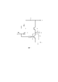
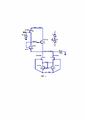
Ближайшим прототипом заявляемого устройства является усилитель сигнала (фиг. 1), представленный в статье Itakura K. et al. A GaAs Bi-FET technology for large scale integration //International Technical Digest on Electron Devices Meeting. – IEEE, 1989. – С. 389-392. (фиг. 7). Схема прототипа фиг. 1 содержит вход 1 и выход 2 устройства, входной полевой транзистор с p-каналом 3, затвор которого соединен со входом 1 устройства, выходной n-p-n биполярный транзистор 4, коллектор которого связан с первой 5 шиной источника питания, а эмиттер подключен к выходу 2 устройства, источник опорного тока 6, включенный между выходом устройства 2 и второй 7 шиной источника питания.The closest prototype of the proposed device is a signal amplifier (Fig. 1), presented in the article by Itakura K. et al. A GaAs Bi-FET technology for large scale integration //International Technical Digest on Electron Devices Meeting. - IEEE, 1989. - S. 389-392. (Fig. 7). Prototype diagram of Fig. 1 contains
Основная задача предполагаемого изобретения состоит в создании повторителя сигнала, обеспечивающего малые значения систематической составляющей напряжения смещения нуля (Uсм), что актуально для построения антиалайзинговых фильтров низких частот, включаемых на входе аналого-цифровых преобразователей [43].The main objective of the proposed invention is to create a signal repeater that provides low values of the systematic component of the zero bias voltage (U cm ), which is relevant for the construction of anti-aliasing low-pass filters included at the input of analog-to-digital converters [43].
Поставленная задача достигается тем, что в повторителе сигнала фиг. 1, содержащем вход 1 и выход 2 устройства, входной полевой транзистор с p-каналом 3, затвор которого соединен со входом 1 устройства, выходной n-p-n биполярный транзистор 4, коллектор которого связан с первой 5 шиной источника питания, а эмиттер подключен к выходу 2 устройства, источник опорного тока 6, включенный между выходом устройства 2 и второй 7 шиной источника питания, предусмотрены новые элементы и связи - сток входного полевого транзистора с p-каналом 3 соединен с первой 5 шиной источника питания, исток соединен с базой выходного n-p-n биполярного транзистора 4 и через прямосмещенный p-n переход на биполярном n-p-n транзисторе 8 связан с выходом устройства 2, при этом источник опорного тока 6 содержит первый 9 и второй 10 вспомогательные полевые транзисторы с p-каналом, затворы которых соединены со второй 7 шиной источника питания, стоки соединены с выходом устройства 2, а истоки объединены и подключены ко второй 7 шине источника питания через два параллельно включенных прямосмещенных p-n перехода на первом 11 и втором 12 вспомогательных n-p-n биполярных транзисторах, коллекторы которых соединены с базами.The task is achieved by the fact that in the signal repeater of FIG. 1 containing
На чертеже фиг. 1 показан усилитель сигнала – прототип, представленный в статье Itakura K. et al. A GaAs Bi-FET technology for large scale integration //International Technical Digest on Electron Devices Meeting. – IEEE, 1989. – С. 389-392. (фиг. 7).In the drawing of FIG. 1 shows the prototype signal amplifier presented in the article by Itakura K. et al. A GaAs Bi-FET technology for large scale integration //International Technical Digest on Electron Devices Meeting. - IEEE, 1989. - S. 389-392. (Fig. 7).
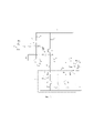
На чертеже фиг. 2 приведена схема заявляемого повторителя сигнала в соответствии с п. 1 формулы изобретения. In the drawing of FIG. 2 shows a diagram of the claimed signal repeater in accordance with
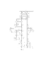
На чертеже фиг. 3 представлен CJFET и CBiJT повторитель сигнала в соответствии с п. 2 формулы изобретения.In the drawing of FIG. 3 shows the CJFET and CBiJT signal repeater according to
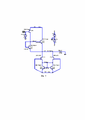
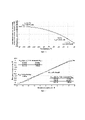
На чертеже фиг. 4 показана схема для моделирования повторителя сигнала фиг. 2 в среде LTspice при t=27oC, +Vcc=-Vee=5 В, Rload=1 МОм на моделях кремниевых транзисторов аналоговых базовых матричных кристаллов АО «Интеграл» (г. Минск) [44,45,46].In the drawing of FIG. 4 shows a circuit for simulating the signal repeater of FIG. 2 in the LTspice environment at t=27 o C, +Vcc=-Vee=5 V, Rload=1 MΩ on models of silicon transistors of analog basic matrix crystals of Integral JSC (Minsk) [44,45,46].
На чертеже фиг. 5 приведена схема для моделирования повторителя сигнала фиг. 2 в среде LTspice при t=-197oC, +Vcc=-Vee=5 В, Rload=1 МОм. In the drawing of FIG. 5 is a diagram for simulating the signal repeater of FIG. 2 in LTspice environment at t=-197 o C, +Vcc=-Vee=5 V, Rload=1 MΩ.
На чертеже фиг. 6 представлена зависимость систематической составляющей напряжения смещения нуля повторителя сигнала фиг. 2 от температуры при +Vcc=-Vee=5 В, Rload=1 Мом.In the drawing of FIG. 6 shows the dependence of the systematic component of the zero bias voltage of the signal follower of FIG. 2 from temperature at +Vcc=-Vee=5 V, Rload=1 Mohm.
На чертеже фиг. 7 показана амплитудная характеристика повторителя сигнала фиг. 4 в среде LTspice при t=27oC, +Vcc=-Vee=5 В, Rload= 5кОм/ 10кОм/1 МОм.In the drawing of FIG. 7 shows the amplitude response of the signal repeater of FIG. 4 in LTspice environment at t=27 o C, +Vcc=-Vee=5V, Rload= 5kΩ/ 10kΩ/1MΩ.
Истоковый повторитель сигнала с малым уровнем систематической составляющей напряжения смещения нуля фиг. 2 содержит вход 1 и выход 2 устройства, входной полевой транзистор с p-каналом 3, затвор которого соединен со входом 1 устройства, выходной n-p-n биполярный транзистор 4, коллектор которого связан с первой 5 шиной источника питания, а эмиттер подключен к выходу 2 устройства, источник опорного тока 6, включенный между выходом устройства 2 и второй 7 шиной источника питания. Сток входного полевого транзистора с p-каналом 3 соединен с первой 5 шиной источника питания, исток соединен с базой выходного n-p-n биполярного транзистора 4 и через прямосмещенный p-n переход на биполярном n-p-n транзисторе 8 связан с выходом устройства 2, при этом источник опорного тока 6 содержит первый 9 и второй 10 вспомогательные полевые транзисторы с p-каналом, затворы которых соединены со второй 7 шиной источника питания, стоки соединены с выходом устройства 2, а истоки объединены и подключены ко второй 7 шине источника питания через два параллельно включенных прямосмещенных p-n перехода на первом 11 и втором 12 вспомогательных n-p-n биполярных транзисторах, коллекторы которых соединены с базами. Source follower with a low systematic component of the zero offset voltage FIG. 2 contains
На чертеже фиг. 2 в качестве элемента нагрузки Rн используется двухполюсник 13.In the drawing of FIG. 2, a two-
На чертеже фиг. 3, в соответствии с п. 2 формулы изобретения, в схему введен первый 14 дополнительный полевой транзистор с n-каналом, затвор которого подключен ко входу 1 устройства, сток соединен со второй 7 шиной источника питания, а исток соединен с базой первого 15 дополнительного p-n-p биполярного транзистора и через первый 16 дополнительный прямосмещенный p-n переход соединен с выходом устройства 2 и эмиттером первого 15 дополнительного p-n-p биполярного транзистора, коллектор которого связан со второй 7 шиной источника питания, причем эмиттер первого 15 дополнительного p-n-p биполярного транзистора соединен со стоками второго 17 и третьего 18 дополнительных полевых транзисторов с n-каналом, затворы которых подключены к первой 5 шине источника питания, а истоки объединены и связаны с первой 5 шиной источника питания через два параллельно включенных p-n перехода 19 и 20, выполненных на p-n-p биполярных транзисторах, коллекторы которых соединены с базами.In the drawing of FIG. 3, in accordance with
Рассмотрим работу предлагаемого повторителя сигнала фиг. 2.Consider the operation of the proposed signal repeater of Fig. 2.
Особенность повторителя сигнала на чертеже фиг. 2 состоит в том, что здесь статический режим транзисторов схемы по току определяется первым 9 и вторым 10 вспомогательными полевыми транзисторами с p-каналом и p-n переходами на первом 11 и втором 12 вспомогательных n-p-n биполярных транзисторах. Это позволяет за счет изменения ширины канала JFET выбирать заданные значения токов входного полевого транзистора с p-каналом 3 и выходного n-p-n биполярного транзистора 4:A feature of the signal repeater in FIG. 2 is that here the static current mode of the transistors of the circuit is determined by the first 9 and second 10 auxiliary field-effect transistors with a p-channel and p-n junctions on the first 11 and second 12 auxiliary n-p-n bipolar transistors. This allows, by changing the width of the JFET channel, to select the specified values of the currents of the input field-effect transistor with p-

где U зи.i – напряжение затвор-исток i-го полевого транзистора при токе истока, равном I R. where U z.i is the gate-source voltage of the i-th field-effect transistor at a source current equal to I R .
Введение новых элементов и связей между ними в соответствии с формулой изобретения позволяет получить малые значения напряжения смещения нуля ПС (фиг. 4, фиг. 5) в широком диапазоне температур (фиг. 6).The introduction of new elements and connections between them in accordance with the claims makes it possible to obtain small values of the bias voltage of zero PS (Fig. 4, Fig. 5) in a wide temperature range (Fig. 6).
Заявляемый повторитель сигнала допускает параметрическую оптимизацию параметров, например, по критерию минимизации систематической составляющей напряжения смещения нуля за счет рационального выбора ширины и длины канала входного полевого транзистора с p-каналом 3.The inventive signal repeater allows parametric optimization of parameters, for example, according to the criterion of minimizing the systematic component of the zero bias voltage due to the rational choice of the width and length of the channel of the input field-effect transistor with a p-
Учитывая, что выходное статическое напряжение предлагаемого ПС измеряется десятками-сотнями микровольт, в соответствии с п. 2 формулы изобретения возможно параллельное (по входу и выходу) включение двух идентичных по схемотехнике, но отличающихся типами каналов входных полевых транзисторов в соответствии с фиг. 3. Это позволяет получить двухтактные повторители напряжения, обеспечивающие токи положительного и отрицательного направлений в более низкоомных нагрузках.Considering that the output static voltage of the proposed PS is measured in tens to hundreds of microvolts, in accordance with
Таким образом, компьютерное моделирование в среде LTspice и оптимизация заявляемой схемы повторителя сигнала показывает, что предлагаемый ПС, схемотехника которого адаптирована на применение в диапазоне низких температур и воздействия проникающей радиации [44,45], имеет существенные достоинства в сравнении с прототипом. Thus, computer simulation in the LTspice environment and optimization of the proposed signal repeater circuit shows that the proposed PS, the circuitry of which is adapted for use in the range of low temperatures and exposure to penetrating radiation [44,45], has significant advantages in comparison with the prototype.
БИБЛИОГРАФИЧЕСКИЙ СПИСОКREFERENCES
1. Патент US 6.215.357, fig. 3, 2001 г.1. Patent US 6.215.357, fig. 3, 2001
2. Патент US 5.351.012, 1994 г. 2. Patent US 5.351.012, 1994
3. Патент US 5.973.534, 1999 г.3. Patent US 5.973.534, 1999
4. Патент US 5.197.124, fig. 25, 1993 г.4. Patent US 5.197.124, fig. 25, 1993
5. Патент US 7.764.123, fig. 3, 2010 г.5. Patent US 7.764.123, fig. 3, 2010
6. Патент US № 6.268.769 fig.3, 2001 г. 6. US patent No. 6.268.769 fig.3, 2001
7. Патент US № 6.420.933, 2002 г.7. US patent No. 6.420.933, 2002
8. Патент US № 5.223.122, 1993 г.8. US Patent No. 5.223.122, 1993
9. Патентная заявка US № 2004/0196101, 2004 г.9. Patent Application US No. 2004/0196101, 2004
10. Патентная заявка US № 2005/0264358 fig.1, 2005 г.10. Patent application US No. 2005/0264358 fig.1, 2005
11. Патентная заявка US № 2002/0175759, 2002 г.11. Patent Application US No. 2002/0175759, 2002
12. Патент US № 5.049.653 fig.8, 1991 г.12. US patent No. 5.049.653 fig.8, 1991
13. Патент US № 4.837.523, 1989 г.13. US patent No. 4.837.523, 1989
14. Патент US № 5.179.355, 1993 г.14. US patent No. 5.179.355, 1993
15. Патент Японии JP 10.163.763, 1991 г.15. Japanese patent JP 10.163.763, 1991
16. Патент Японии JP 10.270.954, 1992 г.16. Japanese patent JP 10.270.954, 1992
17. Патент US № 5.170.134 fig.6, 1992 г.17. US patent No. 5.170.134 fig.6, 1992
18. Патент US № 4.540.950, 1985 г.18. US patent No. 4.540.950, 1985
19. Патент US № 4.424.493, 1984 г.19. US patent No. 4.424.493, 1984
20. Патент Японии JP 6310950, 2018 г. 20. Japanese patent JP 6310950, 2018
21. Патент US № 5.378.938, 1995 г.21. US patent No. 5.378.938, 1995
22. Патент US № 4.827.223, 1989 г.22. US patent No. 4.827.223, 1989
23. Патент US № 6.160.451, 2000 г.23. US patent No. 6.160.451, 2000
24. Патент US № 4.639.685, 1987 г.24. US patent No. 4.639.685, 1987
25. А.св. СССР 1506512, 1986 г.25. A. St. USSR 1506512, 1986
26. Патент US № 5.399.991, 1995 г.26. US patent No. 5.399.991, 1995
27. Патент US № 6.542.032, 2003 г.27. US patent No. 6.542.032, 2003
28. M. Djebbi, A. Assi and M. Sawan. An offset-compensated wide-bandwidth CMOS current-feedback operational amplifier // CCECE 2003 - Canadian Conference on Electrical and Computer Engineering. Toward a Caring and Humane Technology (Cat. No.03CH37436), 2003, pp. 73-76 vol.1. DOI: 10.1109/CCECE.2003.122634728. M. Djebbi, A. Assi and M. Sawan. An offset-compensated wide-bandwidth CMOS current-feedback operational amplifier // CCECE 2003 - Canadian Conference on Electrical and Computer Engineering. Toward a Caring and Humane Technology (Cat. No.03CH37436), 2003, pp. 73-76 vol.1. DOI: 10.1109/CCECE.2003.1226347
29. Butyrlagin, Nikolay; Denisenko, Darya; Prokopenko, Nikolay; Inanov, Yuri (2022): Bank of new schemes of active RC-filters of the Sallen-Key subclass with independent tuning of the main parameters. TechRxiv. Preprint. https://doi.org/10.36227/techrxiv.19614813.v129. Butyrlagin, Nikolay; Denisenko, Darya; Prokopenko, Nikolay; Inanov, Yuri (2022): Bank of new schemes of active RC-filters of the Sallen-Key subclass with independent tuning of the main parameters. TechRxiv. Preprint. https://doi.org/10.36227/techrxiv.19614813.v1
30. Prokopenko, N.; Budyakov, P.; Bugakova, A. Research and Comparative Modeling of the Si, GaAs and GaN JFET/CMOS Buffer Amplifiers for Sallen-Key LPF Design Problems with A Low Offset Voltage's Systematic Component . Preprints 2022, 2022050026 (doi: 10.20944/preprints202205.0026.v1).https://www.preprints.org/manuscript/202205.0026/v130. Prokopenko, N.; Budyakov, P.; Bugakova, A. Research and Comparative Modeling of the Si, GaAs and GaN JFET/CMOS Buffer Amplifiers for Sallen-Key LPF Design Problems with A Low Offset Voltage's Systematic Component . Preprints 2022, 2022050026 (doi: 10.20944/preprints202205.0026.v1). https://www.preprints.org/manuscript/202205.0026/v1
31. Itakura K. et al. A GaAs Bi-FET technology for large scale integration //International Technical Digest on Electron Devices Meeting. – IEEE, 1989. – С. 389-392. (фиг. 7)31. Itakura K. et al. A GaAs Bi-FET technology for large scale integration //International Technical Digest on Electron Devices Meeting. - IEEE, 1989. - S. 389-392. (Fig. 7)
32. Патент RU 2479109, 2013 г. (токовое зеркало на транзисторе 15 в эмиттерной цепи транзистора 2)32. Patent RU 2479109, 2013 (current mirror on
33. Патент RU 2536672, фиг.3 (токовое зеркало 8 в эмиттерной цепи транзистора 2), 2014 г.33. Patent RU 2536672, Fig.3 (
34. Патент GB 2029662, fig. 1, 1979 г. (токовое зеркало (элементы 14, 12) в эмиттерной цепи транзистора 10)34. GB 2029662, fig. 1, 1979 (current mirror (
35. Патент US 4236119 (токовое зеркало на элементах 14 и 12 в эмиттерной цепи транзистора 10) 35. Patent US 4236119 (current mirror on
36. Патентная заявка US 2001/0017571, fig.2, fig. 3 (токовое зеркало на транзисторах 214, 208)36. Patent application US 2001/0017571, fig.2, fig. 3 (current mirror on transistors 214, 208)
37. Патент US 3673508, 1972 г., fig. 1 (токовое зеркало на транзисторе 22 в эмиттерной цепи транзистора 12)37. Patent US 3673508, 1972, fig. 1 (current mirror on transistor 22 in the emitter circuit of transistor 12)
38. Патент ФРГ 2055939, 1971 г., fig. 5 (токовое зеркало на транзисторе Q3 в эмиттерной цепи транзистора Q1)38. German patent 2055939, 1971, fig. 5 (current mirror on transistor Q3 in the emitter circuit of transistor Q1)
39. M. Fresina, "Trends in GaAs HBTs for wireless and RF," 2011 IEEE Bipolar/BiCMOS Circuits and Technology Meeting, Atlanta, GA, USA, 2011, pp. 150-153. doi: 10.1109/BCTM.2011.608276939. M. Fresina, "Trends in GaAs HBTs for wireless and RF," 2011 IEEE Bipolar/BiCMOS Circuits and Technology Meeting, Atlanta, GA, USA, 2011, pp. 150-153. doi:10.1109/BCTM.2011.6082769
40. P. J. Zampardi, M. Sun, C. Cismaru and J. Li, "Prospects for a BiCFET III-V HBT Process," 2012 IEEE Compound Semiconductor Integrated Circuit Symposium (CSICS), La Jolla, CA, USA, 2012, pp. 1-3. doi: 10.1109/CSICS.2012.634011640. P. J. Zampardi, M. Sun, C. Cismaru and J. Li, "Prospects for a BiCFET III-V HBT Process," 2012 IEEE Compound Semiconductor Integrated Circuit Symposium (CSICS), La Jolla, CA, USA, 2012, pp . 1-3. doi:10.1109/CSICS.2012.6340116
41. W. Liu, D. Hill, D. Costa and J. S. Harris, "High-performance microwave AlGaAs-InGaAs Pnp HBT with high-DC current gain," in IEEE Microwave and Guided Wave Letters, vol. 2, no. 8, pp. 331-333, Aug. 1992. doi: 10.1109/75.15360441. W. Liu, D. Hill, D. Costa and J. S. Harris, "High-performance microwave AlGaAs-InGaAs Pnp HBT with high-DC current gain," in IEEE Microwave and Guided Wave Letters, vol. 2, no. 8, pp. 331-333, Aug. 1992. doi: 10.1109/75.153604
42. Peatman W. et al. InGaP-Plus™: advanced GaAs BiFET technology and applications // CS MANTECH Conference, May 14-17, 2007, Austin, Texas, USA. pp. 243-246.42 Peatman W. et al. InGaP-Plus™: advanced GaAs BiFET technology and applications // CS MANTECH Conference, May 14-17, 2007, Austin, Texas, USA. pp. 243-246.
43. Динамические погрешности процесса ввода аналоговых сигналов датчиков в системах управления и контроля: моногр. / Л. К. Самойлов, Д. Ю. Денисенко, Н. Н. Прокопенко. – М.: СОЛОН-Пресс, 2021. – 240 с.43. Dynamic errors in the process of inputting analog signals of sensors in control and monitoring systems: monograph. / L. K. Samoilov, D. Yu. Denisenko, N. N. Prokopenko. – M.: SOLON-Press, 2021. – 240 p.
44. Элементная база радиационно-стойких информационно-измерительных систем: монография / Н.Н. Прокопенко, О.В. Дворников, С.Г. Крутчинский; под общ. ред. д.т.н. проф. Н.Н. Прокопенко; ФГБОУ ВПО «Южно-Рос. гос. ун-т экономики и сервиса». - Шахты: ФГБОУ ВПО «ЮРГУЭС», 2011. - 208 с.44. Element base of radiation-resistant information-measuring systems: monograph / N.N. Prokopenko, O.V. Dvornikov, S.G. Krutchinsky; under total ed. d.t.s. prof. N.N. Prokopenko; FGBOU VPO "South-Ros. state University of Economics and Service”. - Mines: FGBOU VPO "YURGUES", 2011. - 208 p.
45. O. V. Dvornikov, V. L. Dziatlau, N. N. Prokopenko, K. O. Petrosiants, N. V. Kozhukhov and V. A. Tchekhovski. The accounting of the simultaneous exposure of the low temperatures and the penetrating radiation at the circuit simulation of the BiJFET analog interfaces of the sensors // 2017 International Siberian Conference on Control and Communications (SIBCON), Astana, Kazakhstan, 2017, pp. 1-6. DOI: 10.1109/SIBCON.2017.799850745. O. V. Dvornikov, V. L. Dziatlau, N. N. Prokopenko, K. O. Petrosiants, N. V. Kozhukhov and V. A. Tchekhovski. The accounting of the simultaneous exposure of the low temperatures and the penetrating radiation at the circuit simulation of the BiJFET analog interfaces of the sensors // 2017 International Siberian Conference on Control and Communications (SIBCON), Astana, Kazakhstan, 2017, pp. 1-6. DOI: 10.1109/SIBCON.2017.7998507
46. Проектирование низкотемпературных и радиационно-стойких аналоговых микросхем для обработки сигналов датчиков: монография / Н.Н. Прокопенко, О.В. Дворников, А.В. Бугакова. – М.: СОЛОН-Пресс, 2021. – 200 с.46. Design of low-temperature and radiation-resistant analog microcircuits for sensor signal processing: monograph / N.N. Prokopenko, O.V. Dvornikov, A.V. Bugakov. – M.: SOLON-Press, 2021. – 200 p.
Claims (2)
Publications (1)
| Publication Number | Publication Date |
|---|---|
| RU2784373C1 true RU2784373C1 (en) | 2022-11-24 |
Family
ID=
Citations (3)
| Publication number | Priority date | Publication date | Assignee | Title |
|---|---|---|---|---|
| RU2530263C1 (en) * | 2013-05-27 | 2014-10-10 | Федеральное государственное бюджетное образовательное учреждение высшего профессионального образования "Южно-Российский государственный университет экономики и сервиса" (ФГБОУ ВПО "ЮРГУЭС") | Quick-acting source voltage repeater |
| RU2536671C1 (en) * | 2013-06-18 | 2014-12-27 | Федеральное государственное бюджетное образовательное учреждение высшего профессионального образования "Южно-Российский государственный университет экономики и сервиса" (ФГБОУ ВПО "ЮРГУЭС") | Quick-acting source voltage follower |
| US10141897B2 (en) * | 2016-12-07 | 2018-11-27 | Silicon Intergrated Systems Corp. | Source follower |
Patent Citations (3)
| Publication number | Priority date | Publication date | Assignee | Title |
|---|---|---|---|---|
| RU2530263C1 (en) * | 2013-05-27 | 2014-10-10 | Федеральное государственное бюджетное образовательное учреждение высшего профессионального образования "Южно-Российский государственный университет экономики и сервиса" (ФГБОУ ВПО "ЮРГУЭС") | Quick-acting source voltage repeater |
| RU2536671C1 (en) * | 2013-06-18 | 2014-12-27 | Федеральное государственное бюджетное образовательное учреждение высшего профессионального образования "Южно-Российский государственный университет экономики и сервиса" (ФГБОУ ВПО "ЮРГУЭС") | Quick-acting source voltage follower |
| US10141897B2 (en) * | 2016-12-07 | 2018-11-27 | Silicon Intergrated Systems Corp. | Source follower |
Non-Patent Citations (1)
| Title |
|---|
| ITAKURA K. et al., "A GaAs Bi-FET technology for large scale integration", International Technical Digest on Electron Devices Meeting, IEEE, 1989, стр. 389-392. * |
Similar Documents
| Publication | Publication Date | Title |
|---|---|---|
| RU2784373C1 (en) | Source signal follower with a low systematic component of the zero offset voltage | |
| RU2814685C1 (en) | Gallium arsenide operational amplifier for operation in wide temperature range | |
| RU2820562C1 (en) | Gallium arsenide operational amplifier with high gain and low level of systematic component of zero offset voltage | |
| RU2789482C1 (en) | Push-pull gallium arsenide buffer amplifier with a small dead zone of the amplitude characteristic | |
| RU2820341C1 (en) | Gallium arsenide operational amplifier based on "bent" cascode | |
| RU2615068C1 (en) | Bipolar-field differential operational amplifier | |
| RU2788498C1 (en) | Gallium arsenide buffer amplifier on field-effect and bipolar p-n-p transistors | |
| RU2767976C1 (en) | Gallium arsenide power amplifier output stage | |
| RU2687161C1 (en) | Buffer amplifier for operation at low temperatures | |
| RU2771316C1 (en) | Gallium buffer amplifier | |
| RU2766868C1 (en) | Gallium arsenide buffer amplifier | |
| RU2813281C1 (en) | Gallium arsenide operational amplifier based on pnp bipolar and field-effect transistors with control pn junction | |
| RU2784376C1 (en) | GALLIUM ARSENIDE BUFFER AMPLIFIER BASED ON n-CHANNEL FET AND p-n-p BIPOLAR TRANSISTORS | |
| RU2813370C1 (en) | Precision gallium arsenide operational amplifier with low level of systematic component of zero offset voltage and high gain | |
| RU2822157C1 (en) | Operational amplifier based on wide-band semiconductors | |
| RU2786943C1 (en) | Gallium arsenide input differential cascade of class ab of a fast operational amplifier | |
| RU2321159C1 (en) | Cascode differential amplifier | |
| RU2621289C1 (en) | Two-stage differential operational amplifier with higher gain | |
| RU2815912C1 (en) | Resistorless gallium arsenide differential cascade and operational amplifier based on it with low zero offset voltage | |
| RU2788499C1 (en) | Gallium arsenide differential voltage-current converter | |
| RU2849877C1 (en) | Output cascade of a gallium arsenide operational amplifier | |
| RU2411637C1 (en) | Precision operational amplifier with low voltage of zero shift | |
| Chumakov et al. | Precision Operational Amplifier on nJFet Arsenide-Gallium Field Effect Transistors and pnp Bipolar Transistors | |
| RU2812914C1 (en) | Low offset gallium arsenide op amp | |
| Dvornikov et al. | Methodology of Circuit Modeling of Charge-Sensitive Amplifiers Based on Wide-Band-Gap (GaAs, GaN) D-FETs |