KR940001552B1 - 포토리소그래픽 패터닝용 레티클 - Google Patents
포토리소그래픽 패터닝용 레티클 Download PDFInfo
- Publication number
- KR940001552B1 KR940001552B1 KR1019910001685A KR910001685A KR940001552B1 KR 940001552 B1 KR940001552 B1 KR 940001552B1 KR 1019910001685 A KR1019910001685 A KR 1019910001685A KR 910001685 A KR910001685 A KR 910001685A KR 940001552 B1 KR940001552 B1 KR 940001552B1
- Authority
- KR
- South Korea
- Prior art keywords
- pattern
- optical beam
- phase shift
- transparent
- reticle
- Prior art date
- Legal status (The legal status is an assumption and is not a legal conclusion. Google has not performed a legal analysis and makes no representation as to the accuracy of the status listed.)
- Expired - Fee Related
Links
Images
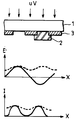


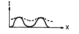


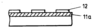

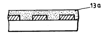


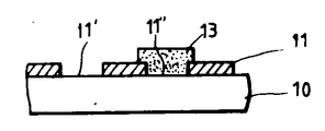
Classifications
-
- G—PHYSICS
- G03—PHOTOGRAPHY; CINEMATOGRAPHY; ANALOGOUS TECHNIQUES USING WAVES OTHER THAN OPTICAL WAVES; ELECTROGRAPHY; HOLOGRAPHY
- G03F—PHOTOMECHANICAL PRODUCTION OF TEXTURED OR PATTERNED SURFACES, e.g. FOR PRINTING, FOR PROCESSING OF SEMICONDUCTOR DEVICES; MATERIALS THEREFOR; ORIGINALS THEREFOR; APPARATUS SPECIALLY ADAPTED THEREFOR
- G03F1/00—Originals for photomechanical production of textured or patterned surfaces, e.g., masks, photo-masks, reticles; Mask blanks or pellicles therefor; Containers specially adapted therefor; Preparation thereof
- G03F1/62—Pellicles, e.g. pellicle assemblies, e.g. having membrane on support frame; Preparation thereof
-
- G—PHYSICS
- G03—PHOTOGRAPHY; CINEMATOGRAPHY; ANALOGOUS TECHNIQUES USING WAVES OTHER THAN OPTICAL WAVES; ELECTROGRAPHY; HOLOGRAPHY
- G03F—PHOTOMECHANICAL PRODUCTION OF TEXTURED OR PATTERNED SURFACES, e.g. FOR PRINTING, FOR PROCESSING OF SEMICONDUCTOR DEVICES; MATERIALS THEREFOR; ORIGINALS THEREFOR; APPARATUS SPECIALLY ADAPTED THEREFOR
- G03F1/00—Originals for photomechanical production of textured or patterned surfaces, e.g., masks, photo-masks, reticles; Mask blanks or pellicles therefor; Containers specially adapted therefor; Preparation thereof
- G03F1/26—Phase shift masks [PSM]; PSM blanks; Preparation thereof
- G03F1/30—Alternating PSM, e.g. Levenson-Shibuya PSM; Preparation thereof
-
- G—PHYSICS
- G03—PHOTOGRAPHY; CINEMATOGRAPHY; ANALOGOUS TECHNIQUES USING WAVES OTHER THAN OPTICAL WAVES; ELECTROGRAPHY; HOLOGRAPHY
- G03F—PHOTOMECHANICAL PRODUCTION OF TEXTURED OR PATTERNED SURFACES, e.g. FOR PRINTING, FOR PROCESSING OF SEMICONDUCTOR DEVICES; MATERIALS THEREFOR; ORIGINALS THEREFOR; APPARATUS SPECIALLY ADAPTED THEREFOR
- G03F1/00—Originals for photomechanical production of textured or patterned surfaces, e.g., masks, photo-masks, reticles; Mask blanks or pellicles therefor; Containers specially adapted therefor; Preparation thereof
- G03F1/26—Phase shift masks [PSM]; PSM blanks; Preparation thereof
Landscapes
- Physics & Mathematics (AREA)
- General Physics & Mathematics (AREA)
- Preparing Plates And Mask In Photomechanical Process (AREA)
- Exposure And Positioning Against Photoresist Photosensitive Materials (AREA)
- Exposure Of Semiconductors, Excluding Electron Or Ion Beam Exposure (AREA)
Applications Claiming Priority (2)
| Application Number | Priority Date | Filing Date | Title |
|---|---|---|---|
| JP2020496A JPH03228053A (ja) | 1990-02-01 | 1990-02-01 | 光露光レチクル |
| JP02-20496 | 1990-02-01 |
Publications (2)
| Publication Number | Publication Date |
|---|---|
| KR920000006A KR920000006A (ko) | 1992-01-10 |
| KR940001552B1 true KR940001552B1 (ko) | 1994-02-24 |
Family
ID=12028772
Family Applications (1)
| Application Number | Title | Priority Date | Filing Date |
|---|---|---|---|
| KR1019910001685A Expired - Fee Related KR940001552B1 (ko) | 1990-02-01 | 1991-01-31 | 포토리소그래픽 패터닝용 레티클 |
Country Status (5)
| Country | Link |
|---|---|
| US (1) | US5126220A (de) |
| EP (1) | EP0440467B1 (de) |
| JP (1) | JPH03228053A (de) |
| KR (1) | KR940001552B1 (de) |
| DE (1) | DE69115062T2 (de) |
Families Citing this family (23)
| Publication number | Priority date | Publication date | Assignee | Title |
|---|---|---|---|---|
| EP0477035B1 (de) * | 1990-09-21 | 1999-12-29 | Dai Nippon Printing Co., Ltd. | Verfahren zur Herstellung einer Phasenverschiebungs-Photomaske |
| US5660956A (en) * | 1990-11-29 | 1997-08-26 | Kabushiki Kaisha Toshiba | Reticle and method of fabricating reticle |
| US5595844A (en) * | 1990-11-29 | 1997-01-21 | Kabushiki Kaisha Toshiba | Method of exposing light in a method of fabricating a reticle |
| JPH0567558A (ja) * | 1991-09-06 | 1993-03-19 | Nikon Corp | 露光方法 |
| JP2595149B2 (ja) * | 1991-09-25 | 1997-03-26 | 株式会社日立製作所 | 電子線描画装置 |
| JP2874406B2 (ja) * | 1991-10-09 | 1999-03-24 | 株式会社日立製作所 | 位相シフタマスクの欠陥修正方法 |
| SG50543A1 (en) * | 1991-11-22 | 1998-07-20 | At & T Corp | Fabrication of phase-shifting lithographic masks |
| US5300786A (en) * | 1992-10-28 | 1994-04-05 | International Business Machines Corporation | Optical focus phase shift test pattern, monitoring system and process |
| US5376483A (en) * | 1993-10-07 | 1994-12-27 | Micron Semiconductor, Inc. | Method of making masks for phase shifting lithography |
| US5470681A (en) * | 1993-12-23 | 1995-11-28 | International Business Machines Corporation | Phase shift mask using liquid phase oxide deposition |
| US5487962A (en) * | 1994-05-11 | 1996-01-30 | Rolfson; J. Brett | Method of chromeless phase shift mask fabrication suitable for auto-cad layout |
| US5495959A (en) * | 1994-05-11 | 1996-03-05 | Micron Technology, Inc. | Method of making substractive rim phase shifting masks |
| US5414580A (en) * | 1994-05-13 | 1995-05-09 | International Business Machines Corporation | Magnetic storage system using thin film magnetic recording heads using phase-shifting mask |
| US5468578A (en) * | 1994-09-26 | 1995-11-21 | Micron Technology, Inc. | Method of making masks for phase shifting lithography to avoid phase conflicts |
| US5766829A (en) * | 1995-05-30 | 1998-06-16 | Micron Technology, Inc. | Method of phase shift lithography |
| US5536606A (en) * | 1995-05-30 | 1996-07-16 | Micron Technology, Inc. | Method for making self-aligned rim phase shifting masks for sub-micron lithography |
| KR100263034B1 (ko) * | 1995-12-02 | 2000-08-01 | 김지태 | 인텔리전트 금고 |
| US6057587A (en) * | 1997-08-28 | 2000-05-02 | Vlsi Technology, Inc. | Semiconductor device with anti-reflective structure |
| KR20020021907A (ko) * | 2000-09-18 | 2002-03-23 | 신형인 | 내피로 특성이 개선된 타이어용 고무조성물 |
| US6859997B1 (en) | 2000-09-19 | 2005-03-01 | Western Digital (Fremont), Inc. | Method for manufacturing a magnetic write element |
| DE10228546B4 (de) * | 2002-06-26 | 2006-08-10 | Infineon Technologies Ag | Verfahren zur Strukturierung einer Lithographiemaske |
| JP5270142B2 (ja) * | 2007-12-05 | 2013-08-21 | 浜松ホトニクス株式会社 | 反射型空間光変調素子 |
| SE1550411A1 (en) * | 2015-04-07 | 2016-10-08 | Fingerprint Cards Ab | Electronic device comprising fingerprint sensor |
Family Cites Families (4)
| Publication number | Priority date | Publication date | Assignee | Title |
|---|---|---|---|---|
| EP0090924B1 (de) * | 1982-04-05 | 1987-11-11 | International Business Machines Corporation | Verfahren zur Erhöhung der Bildauflösung einer Photomaske und Photomaske zur Dürchführung dieses Verfahrens |
| JPS61128251A (ja) * | 1984-11-26 | 1986-06-16 | Mitsubishi Electric Corp | X線露光用マスク |
| JPH0682604B2 (ja) * | 1987-08-04 | 1994-10-19 | 三菱電機株式会社 | X線マスク |
| JP2710967B2 (ja) * | 1988-11-22 | 1998-02-10 | 株式会社日立製作所 | 集積回路装置の製造方法 |
-
1990
- 1990-02-01 JP JP2020496A patent/JPH03228053A/ja active Pending
-
1991
- 1991-01-31 EP EP91300753A patent/EP0440467B1/de not_active Expired - Lifetime
- 1991-01-31 US US07/648,697 patent/US5126220A/en not_active Expired - Lifetime
- 1991-01-31 DE DE69115062T patent/DE69115062T2/de not_active Expired - Fee Related
- 1991-01-31 KR KR1019910001685A patent/KR940001552B1/ko not_active Expired - Fee Related
Also Published As
| Publication number | Publication date |
|---|---|
| DE69115062T2 (de) | 1996-05-09 |
| KR920000006A (ko) | 1992-01-10 |
| DE69115062D1 (de) | 1996-01-18 |
| US5126220A (en) | 1992-06-30 |
| JPH03228053A (ja) | 1991-10-09 |
| EP0440467A2 (de) | 1991-08-07 |
| EP0440467B1 (de) | 1995-12-06 |
| EP0440467A3 (en) | 1991-10-30 |
Similar Documents
| Publication | Publication Date | Title |
|---|---|---|
| US5126220A (en) | Reticle for photolithographic patterning | |
| US5275896A (en) | Single-alignment-level lithographic technique for achieving self-aligned features | |
| JP3105234B2 (ja) | 半導体装置の製造方法 | |
| EP0577297B1 (de) | Selbstausrichtendes Verfahren zur Herstellung von Phasenverschiebungsmasken, die drei oder mehr Phasenverschieber besitzen | |
| US5405721A (en) | Phase-shifting lithographic masks having phase-shifting layers of differing compositions | |
| KR100190358B1 (ko) | 투영 포토리소그래피용 위상 시프트 마스크 및 이의 제조방법 | |
| US5244759A (en) | Single-alignment-level lithographic technique for achieving self-aligned features | |
| EP0475694B1 (de) | Optische Phasenmaske und Verfahren zur Herstellung | |
| US3758326A (en) | Mask or original for reproducing patterns on light sensitive layers | |
| US5300378A (en) | Method of producing a phase shifting mask | |
| JP2641362B2 (ja) | リソグラフィー方法および位相シフトマスクの作製方法 | |
| KR0135149B1 (ko) | 위상반전 마스크의 제조방법 | |
| US5468576A (en) | Method for manufacturing exposure mask | |
| KR950007477B1 (ko) | 위상반전 마스크 및 그의 제조방법 | |
| JP2652341B2 (ja) | 位相反転マスクの製造方法 | |
| CN112925164A (zh) | 光掩膜板及其形成方法 | |
| JP2783582B2 (ja) | フォトマスク | |
| JP4099836B2 (ja) | ハーフトーン型位相シフトマスク用ブランク及びその製造方法及びハーフトーン型位相シフトマスク | |
| JPH07281414A (ja) | 位相シフトマスクブランク及び位相シフトマスクとその製造方法 | |
| KR0151228B1 (ko) | 고립된 다수의 패턴을 형성하기 위한 포토마스크 | |
| KR100790565B1 (ko) | 포토 마스크 | |
| JP2739008B2 (ja) | 位相シフトマスク及びその製造方法 | |
| KR19990050484A (ko) | 하프-톤 위상 반전 마스크의 제조 방법 | |
| KR940011095B1 (ko) | 위상반전마스크, 그의 제조방법 및 그를 이용한 패턴형성방법 | |
| JP2913753B2 (ja) | 位相シフトマスクの製造方法 |
Legal Events
| Date | Code | Title | Description |
|---|---|---|---|
| A201 | Request for examination | ||
| PA0109 | Patent application |
St.27 status event code: A-0-1-A10-A12-nap-PA0109 |
|
| PA0201 | Request for examination |
St.27 status event code: A-1-2-D10-D11-exm-PA0201 |
|
| R17-X000 | Change to representative recorded |
St.27 status event code: A-3-3-R10-R17-oth-X000 |
|
| PG1501 | Laying open of application |
St.27 status event code: A-1-1-Q10-Q12-nap-PG1501 |
|
| G160 | Decision to publish patent application | ||
| PG1605 | Publication of application before grant of patent |
St.27 status event code: A-2-2-Q10-Q13-nap-PG1605 |
|
| E701 | Decision to grant or registration of patent right | ||
| PE0701 | Decision of registration |
St.27 status event code: A-1-2-D10-D22-exm-PE0701 |
|
| GRNT | Written decision to grant | ||
| PR0701 | Registration of establishment |
St.27 status event code: A-2-4-F10-F11-exm-PR0701 |
|
| PR1002 | Payment of registration fee |
St.27 status event code: A-2-2-U10-U11-oth-PR1002 Fee payment year number: 1 |
|
| PR1001 | Payment of annual fee |
St.27 status event code: A-4-4-U10-U11-oth-PR1001 Fee payment year number: 4 |
|
| PR1001 | Payment of annual fee |
St.27 status event code: A-4-4-U10-U11-oth-PR1001 Fee payment year number: 5 |
|
| PN2301 | Change of applicant |
St.27 status event code: A-5-5-R10-R13-asn-PN2301 St.27 status event code: A-5-5-R10-R11-asn-PN2301 |
|
| PN2301 | Change of applicant |
St.27 status event code: A-5-5-R10-R13-asn-PN2301 St.27 status event code: A-5-5-R10-R11-asn-PN2301 |
|
| PR1001 | Payment of annual fee |
St.27 status event code: A-4-4-U10-U11-oth-PR1001 Fee payment year number: 6 |
|
| R18-X000 | Changes to party contact information recorded |
St.27 status event code: A-5-5-R10-R18-oth-X000 |
|
| R18-X000 | Changes to party contact information recorded |
St.27 status event code: A-5-5-R10-R18-oth-X000 |
|
| PR1001 | Payment of annual fee |
St.27 status event code: A-4-4-U10-U11-oth-PR1001 Fee payment year number: 7 |
|
| PN2301 | Change of applicant |
St.27 status event code: A-5-5-R10-R13-asn-PN2301 St.27 status event code: A-5-5-R10-R11-asn-PN2301 |
|
| PR1001 | Payment of annual fee |
St.27 status event code: A-4-4-U10-U11-oth-PR1001 Fee payment year number: 8 |
|
| PR1001 | Payment of annual fee |
St.27 status event code: A-4-4-U10-U11-oth-PR1001 Fee payment year number: 9 |
|
| PR1001 | Payment of annual fee |
St.27 status event code: A-4-4-U10-U11-oth-PR1001 Fee payment year number: 10 |
|
| FPAY | Annual fee payment |
Payment date: 20040205 Year of fee payment: 11 |
|
| PR1001 | Payment of annual fee |
St.27 status event code: A-4-4-U10-U11-oth-PR1001 Fee payment year number: 11 |
|
| LAPS | Lapse due to unpaid annual fee | ||
| PC1903 | Unpaid annual fee |
St.27 status event code: A-4-4-U10-U13-oth-PC1903 Not in force date: 20050225 Payment event data comment text: Termination Category : DEFAULT_OF_REGISTRATION_FEE |
|
| PC1903 | Unpaid annual fee |
St.27 status event code: N-4-6-H10-H13-oth-PC1903 Ip right cessation event data comment text: Termination Category : DEFAULT_OF_REGISTRATION_FEE Not in force date: 20050225 |
|
| P22-X000 | Classification modified |
St.27 status event code: A-4-4-P10-P22-nap-X000 |