EP0440467A2 - Maske für photolithographische Strukturierung - Google Patents
Maske für photolithographische Strukturierung Download PDFInfo
- Publication number
- EP0440467A2 EP0440467A2 EP91300753A EP91300753A EP0440467A2 EP 0440467 A2 EP0440467 A2 EP 0440467A2 EP 91300753 A EP91300753 A EP 91300753A EP 91300753 A EP91300753 A EP 91300753A EP 0440467 A2 EP0440467 A2 EP 0440467A2
- Authority
- EP
- European Patent Office
- Prior art keywords
- pattern
- optical beam
- major surface
- phase shift
- transparent
- Prior art date
- Legal status (The legal status is an assumption and is not a legal conclusion. Google has not performed a legal analysis and makes no representation as to the accuracy of the status listed.)
- Granted
Links
Images

Classifications
-
- G—PHYSICS
- G03—PHOTOGRAPHY; CINEMATOGRAPHY; ANALOGOUS TECHNIQUES USING WAVES OTHER THAN OPTICAL WAVES; ELECTROGRAPHY; HOLOGRAPHY
- G03F—PHOTOMECHANICAL PRODUCTION OF TEXTURED OR PATTERNED SURFACES, e.g. FOR PRINTING, FOR PROCESSING OF SEMICONDUCTOR DEVICES; MATERIALS THEREFOR; ORIGINALS THEREFOR; APPARATUS SPECIALLY ADAPTED THEREFOR
- G03F1/00—Originals for photomechanical production of textured or patterned surfaces, e.g., masks, photo-masks, reticles; Mask blanks or pellicles therefor; Containers specially adapted therefor; Preparation thereof
- G03F1/62—Pellicles, e.g. pellicle assemblies, e.g. having membrane on support frame; Preparation thereof
-
- G—PHYSICS
- G03—PHOTOGRAPHY; CINEMATOGRAPHY; ANALOGOUS TECHNIQUES USING WAVES OTHER THAN OPTICAL WAVES; ELECTROGRAPHY; HOLOGRAPHY
- G03F—PHOTOMECHANICAL PRODUCTION OF TEXTURED OR PATTERNED SURFACES, e.g. FOR PRINTING, FOR PROCESSING OF SEMICONDUCTOR DEVICES; MATERIALS THEREFOR; ORIGINALS THEREFOR; APPARATUS SPECIALLY ADAPTED THEREFOR
- G03F1/00—Originals for photomechanical production of textured or patterned surfaces, e.g., masks, photo-masks, reticles; Mask blanks or pellicles therefor; Containers specially adapted therefor; Preparation thereof
- G03F1/26—Phase shift masks [PSM]; PSM blanks; Preparation thereof
- G03F1/30—Alternating PSM, e.g. Levenson-Shibuya PSM; Preparation thereof
-
- G—PHYSICS
- G03—PHOTOGRAPHY; CINEMATOGRAPHY; ANALOGOUS TECHNIQUES USING WAVES OTHER THAN OPTICAL WAVES; ELECTROGRAPHY; HOLOGRAPHY
- G03F—PHOTOMECHANICAL PRODUCTION OF TEXTURED OR PATTERNED SURFACES, e.g. FOR PRINTING, FOR PROCESSING OF SEMICONDUCTOR DEVICES; MATERIALS THEREFOR; ORIGINALS THEREFOR; APPARATUS SPECIALLY ADAPTED THEREFOR
- G03F1/00—Originals for photomechanical production of textured or patterned surfaces, e.g., masks, photo-masks, reticles; Mask blanks or pellicles therefor; Containers specially adapted therefor; Preparation thereof
- G03F1/26—Phase shift masks [PSM]; PSM blanks; Preparation thereof
Definitions
- the present invention generally relates to photolithographic patterning of semiconductor devices and more particularly to a reticle used for the photolithographic patterning process to form a device pattern on a semiconductor wafer by an ultraviolet or deep ultraviolet light.
- the large scale integrated circuits has increased the integration density by about four times in the last three or four years.
- the demand for increasing the integration density persists and various patterning processes are under investigation for forming extremely fine semiconductor patterns on a semiconductor wafer with an improved resolution.
- the photolithographic patterning process that uses ultraviolet or deep ultraviolet lights for the patterning is one of the major patterning processes currently used.
- This process uses a mask or reticle carrying thereon a semiconductor pattern in an enlarged scale and is particularly advantageous for mass producing the semiconductor devices with large throughput.
- the process relies upon the photochemical reaction in the photoresist caused by the ultraviolet light that has passed through the reticle and associated therewith, has an inherent problem of poor resolution due to the diffraction of light at the edge of the reticle pattern. This problem becomes particularly acute when the size of the semiconductor pattern to be written on the wafer is decreased in correspondence to the increased integration density.
- the reticles for the photolithographic patterning have conventionally been produced by patterning a metal layer grown on a substrate by electron beam or ultraviolet beam.
- the reticle thus produced is used in a photolithographic exposure system for selectively interrupting an ultraviolet or deep ultraviolet beam used for exposing the photoresist covering the wafer, according to the desired semiconductor pattern.
- FIGS.1(A) - 1(C) show the principle of suppressing the Fresnel diffraction proposed in the foregoing reference.
- a glass substrate 1 is provided with an opaque pattern 3 of chromium and the like that selectively interrupts an ultraviolet light designated as UV according to a desired semiconductor pattern. Further a phase shift pattern 2 is provided between a pair of adjacent opaque patterns 3 for shifting the phase of the ultraviolet light passing therethrough with respect to the ultraviolet light that has passed through the reticle without being modified the phase by the phase shift pattern 2.
- FIG.1(B) shows a typical distribution of the electric field E of transmitted light beam that has passed through the reticle
- FIG.1(C) shows the corresponding distribution of the intensity of the light beam
- the solid line represents the case where the phase shift pattern 2 is provided
- the broken line represents the case where no such phase shift pattern is provided.
- the transmitted light beam has a finite intensity even in the region immediately under the opaque pattern 3 when the phase shift pattern 2 is not provided, because of the diffraction of the light.
- the phase of the light beam that has passed through the pattern 2 can be made opposed with respect to the light beam that has passed through the reticle without being shifted the phase thereof.
- the phase shift pattern 2 has been formed of an insulating material such as silicon oxide or organic material.
- an electron beam lithography there has been a problem in that electrons are accumulated in the insulating film forming the pattern 2 as well as in organic resist 4 as shown in FIG.2, and the electron beam is offset from the aimed point because of the coulomb repulsion. Because of this problem, the conventional reticle could not be formed with satisfactorily high resolution.
- Another and more specific object of the present invention is to provide a reticle that does not cause charge-up during the fabrication process when irradiated by a charged particle beam.
- Another object of the present invention is to provide a reticle comprising an optically transparent substrate, an opaque pattern provided on the substrate for interrupting a light beam incident to the substrate, said opaque pattern being formed with a transparent pattern to pass the light beam shaped according to a desired semiconductor pattern, and a phase shift pattern provided on the substrate in correspondence to the light beam that has passed through the transparent pattern for shifting a phase of the light beam, wherein said phase shift pattern comprises an optically transparent and electrically conductive material.
- the patterning process of the phase shift pattern by charged beam lithography such as the electron beam lithography does not cause charge-up of the material forming the phase shift pattern or resist employed for the patterning, and an accurate patterning of the phase shift pattern becomes possible.
- efficient cancellation of the diffraction by the phase shift pattern becomes possible even when the size of the semiconductor device to be projected becomes extremely small.
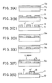
- FIGS.3(A) - 3(G) are the diagrams showing the process of forming the reticle according to an embodiment of the present invention.
- an opaque film 11a of chromium or chromium oxide is deposited on a quartz substrate having a thickness of typically 1.5 - 2.0 mm. Further, a resist 12a is deposited on the opaque film 11a as illustrated.
- the resist 12a is patterned by an electron beam exposure process to form a patterned resist 12 according to a desired device pattern.
- the opaque film 11a is patterned in a step of FIG.3(C) by a dry etching or wet etching process, using the patterned resist 12 as the mask.
- an opaque reticle pattern 11 is formed in correspondence to the device pattern carried by the patterned resist 12a as illustrated, leaving transparent regions 11′ and 11 ⁇ between the patterns 11.
- a layer 13a of an electrically conductive transparent material such as indium tin oxide (In2O3.SnO2) commonly known as ITO or tin oxide (SnO2) is deposited on the substrate 10 to bury the reticle pattern 11 underneath as illustrated in FIG.3(C).
- the canceling of the diffraction by the phase shift pattern as described with reference to FIGS.1(A) - 1(C) can be achieved when the foregoing relation is satisfied.
- the thickness ⁇ that satisfies the foregoing relationship is determined to be 0.2 ⁇ m.
- the layer 13a is a conductive film.
- a resist 14a is deposited on the layer 13a as shown in FIG.3(E), and the resist 14a is patterned by an electron beam according to a desired phase shift pattern to form a patterned resist 14 as shown in FIG.3(F).
- the electrons incident to the resist 14 as the electron beam are immediately dissipated through the conductive layer 13a to the ground and no charge-up occurs in the resist 14 or in the layer 13a.
- the electron beam used for the patterning of the resist 14a hits the resist accurately. No stray of the electron beam spot by the charge-up occurs in this process.
- the layer 13a is patterned using the patterned resist 14 as the mask and a desired phase shift pattern 13 is obtained as shown in FIG.3(G).
- the phase shift pattern 13 is provided in correspondence to the transparent region 11 ⁇ while the adjacent transparent region 11′ is left not covered by the phase shift pattern 13.
- the canceling of diffraction of the ultraviolet light beams that have passed through the region 11′ and the region 11 ⁇ is achieved as explained with reference to FIGS.1(A) - 1(C).
- the patterning of the step of FIG.3(G) is achieved by a dry etching process using a mixture of CH4/H2 with a gas pressure of 5 X 10 ⁇ 3 torr and an RF power of 300 watts for 3 - 5 minutes.
- the temperature of the substrate is set to 70 °C.
- CH4 butyl acetate or carbon tetrachloride may be used. The duration is of course adjusted to obtain the necessary thickness described previously.
- the layer 13a is made of SnO2
- a mixture of hydrogen and butyl acetate containing 40 % of butyl acetate may be used.
- the pressure is set to about 10 ⁇ 3 torr and an RF power of 200 - 500 watts is applied for about one minute.
- the phase shift pattern 13 can be formed with high precision and thereby an effective cancellation of diffraction is achieved.
Landscapes
- Physics & Mathematics (AREA)
- General Physics & Mathematics (AREA)
- Preparing Plates And Mask In Photomechanical Process (AREA)
- Exposure And Positioning Against Photoresist Photosensitive Materials (AREA)
- Exposure Of Semiconductors, Excluding Electron Or Ion Beam Exposure (AREA)
Applications Claiming Priority (2)
| Application Number | Priority Date | Filing Date | Title |
|---|---|---|---|
| JP2020496A JPH03228053A (ja) | 1990-02-01 | 1990-02-01 | 光露光レチクル |
| JP20496/90 | 1990-02-01 |
Publications (3)
| Publication Number | Publication Date |
|---|---|
| EP0440467A2 true EP0440467A2 (de) | 1991-08-07 |
| EP0440467A3 EP0440467A3 (en) | 1991-10-30 |
| EP0440467B1 EP0440467B1 (de) | 1995-12-06 |
Family
ID=12028772
Family Applications (1)
| Application Number | Title | Priority Date | Filing Date |
|---|---|---|---|
| EP91300753A Expired - Lifetime EP0440467B1 (de) | 1990-02-01 | 1991-01-31 | Maske für photolithographische Strukturierung |
Country Status (5)
| Country | Link |
|---|---|
| US (1) | US5126220A (de) |
| EP (1) | EP0440467B1 (de) |
| JP (1) | JPH03228053A (de) |
| KR (1) | KR940001552B1 (de) |
| DE (1) | DE69115062T2 (de) |
Cited By (1)
| Publication number | Priority date | Publication date | Assignee | Title |
|---|---|---|---|---|
| EP0477035A3 (en) * | 1990-09-21 | 1992-10-21 | Dai Nippon Printing Co., Ltd. | Phase shift layer-containing photomask, and its production and correction |
Families Citing this family (22)
| Publication number | Priority date | Publication date | Assignee | Title |
|---|---|---|---|---|
| US5660956A (en) * | 1990-11-29 | 1997-08-26 | Kabushiki Kaisha Toshiba | Reticle and method of fabricating reticle |
| US5595844A (en) * | 1990-11-29 | 1997-01-21 | Kabushiki Kaisha Toshiba | Method of exposing light in a method of fabricating a reticle |
| JPH0567558A (ja) * | 1991-09-06 | 1993-03-19 | Nikon Corp | 露光方法 |
| JP2595149B2 (ja) * | 1991-09-25 | 1997-03-26 | 株式会社日立製作所 | 電子線描画装置 |
| JP2874406B2 (ja) * | 1991-10-09 | 1999-03-24 | 株式会社日立製作所 | 位相シフタマスクの欠陥修正方法 |
| SG50543A1 (en) * | 1991-11-22 | 1998-07-20 | At & T Corp | Fabrication of phase-shifting lithographic masks |
| US5300786A (en) * | 1992-10-28 | 1994-04-05 | International Business Machines Corporation | Optical focus phase shift test pattern, monitoring system and process |
| US5376483A (en) * | 1993-10-07 | 1994-12-27 | Micron Semiconductor, Inc. | Method of making masks for phase shifting lithography |
| US5470681A (en) * | 1993-12-23 | 1995-11-28 | International Business Machines Corporation | Phase shift mask using liquid phase oxide deposition |
| US5487962A (en) * | 1994-05-11 | 1996-01-30 | Rolfson; J. Brett | Method of chromeless phase shift mask fabrication suitable for auto-cad layout |
| US5495959A (en) * | 1994-05-11 | 1996-03-05 | Micron Technology, Inc. | Method of making substractive rim phase shifting masks |
| US5414580A (en) * | 1994-05-13 | 1995-05-09 | International Business Machines Corporation | Magnetic storage system using thin film magnetic recording heads using phase-shifting mask |
| US5468578A (en) * | 1994-09-26 | 1995-11-21 | Micron Technology, Inc. | Method of making masks for phase shifting lithography to avoid phase conflicts |
| US5766829A (en) * | 1995-05-30 | 1998-06-16 | Micron Technology, Inc. | Method of phase shift lithography |
| US5536606A (en) * | 1995-05-30 | 1996-07-16 | Micron Technology, Inc. | Method for making self-aligned rim phase shifting masks for sub-micron lithography |
| KR100263034B1 (ko) * | 1995-12-02 | 2000-08-01 | 김지태 | 인텔리전트 금고 |
| US6057587A (en) * | 1997-08-28 | 2000-05-02 | Vlsi Technology, Inc. | Semiconductor device with anti-reflective structure |
| KR20020021907A (ko) * | 2000-09-18 | 2002-03-23 | 신형인 | 내피로 특성이 개선된 타이어용 고무조성물 |
| US6859997B1 (en) | 2000-09-19 | 2005-03-01 | Western Digital (Fremont), Inc. | Method for manufacturing a magnetic write element |
| DE10228546B4 (de) * | 2002-06-26 | 2006-08-10 | Infineon Technologies Ag | Verfahren zur Strukturierung einer Lithographiemaske |
| JP5270142B2 (ja) * | 2007-12-05 | 2013-08-21 | 浜松ホトニクス株式会社 | 反射型空間光変調素子 |
| SE1550411A1 (en) * | 2015-04-07 | 2016-10-08 | Fingerprint Cards Ab | Electronic device comprising fingerprint sensor |
Family Cites Families (4)
| Publication number | Priority date | Publication date | Assignee | Title |
|---|---|---|---|---|
| EP0090924B1 (de) * | 1982-04-05 | 1987-11-11 | International Business Machines Corporation | Verfahren zur Erhöhung der Bildauflösung einer Photomaske und Photomaske zur Dürchführung dieses Verfahrens |
| JPS61128251A (ja) * | 1984-11-26 | 1986-06-16 | Mitsubishi Electric Corp | X線露光用マスク |
| JPH0682604B2 (ja) * | 1987-08-04 | 1994-10-19 | 三菱電機株式会社 | X線マスク |
| JP2710967B2 (ja) * | 1988-11-22 | 1998-02-10 | 株式会社日立製作所 | 集積回路装置の製造方法 |
-
1990
- 1990-02-01 JP JP2020496A patent/JPH03228053A/ja active Pending
-
1991
- 1991-01-31 EP EP91300753A patent/EP0440467B1/de not_active Expired - Lifetime
- 1991-01-31 US US07/648,697 patent/US5126220A/en not_active Expired - Lifetime
- 1991-01-31 DE DE69115062T patent/DE69115062T2/de not_active Expired - Fee Related
- 1991-01-31 KR KR1019910001685A patent/KR940001552B1/ko not_active Expired - Fee Related
Non-Patent Citations (1)
| Title |
|---|
| IEEE TRANSACTIONS ON ELECTRON DEVICES. vol. 11, no. 12, December 1982, NEW YORK US pages 1828 - 1836; M. D. LEVENSON et al.: "Improving Resolution in Photolithography with a Phase-Shifting Mask" * |
Cited By (1)
| Publication number | Priority date | Publication date | Assignee | Title |
|---|---|---|---|---|
| EP0477035A3 (en) * | 1990-09-21 | 1992-10-21 | Dai Nippon Printing Co., Ltd. | Phase shift layer-containing photomask, and its production and correction |
Also Published As
| Publication number | Publication date |
|---|---|
| DE69115062T2 (de) | 1996-05-09 |
| KR920000006A (ko) | 1992-01-10 |
| DE69115062D1 (de) | 1996-01-18 |
| US5126220A (en) | 1992-06-30 |
| JPH03228053A (ja) | 1991-10-09 |
| EP0440467B1 (de) | 1995-12-06 |
| KR940001552B1 (ko) | 1994-02-24 |
| EP0440467A3 (en) | 1991-10-30 |
Similar Documents
| Publication | Publication Date | Title |
|---|---|---|
| EP0440467B1 (de) | Maske für photolithographische Strukturierung | |
| JP2593601B2 (ja) | 位相シフトマスクの作製方法 | |
| US6632593B2 (en) | Pattern-forming method using photomask, and pattern-forming apparatus | |
| US5595844A (en) | Method of exposing light in a method of fabricating a reticle | |
| JPH06266095A (ja) | レティクル及びレティクル・ブランク | |
| US5382483A (en) | Self-aligned phase-shifting mask | |
| EP0475694B1 (de) | Optische Phasenmaske und Verfahren zur Herstellung | |
| JP2022029394A (ja) | 極紫外線リソグラフィ用ペリクル及びその製造方法 | |
| US8563227B2 (en) | Method and system for exposure of a phase shift mask | |
| EP0489540A2 (de) | Lithographische Phasenverschiebungsmasken mit erhöhter Auflösung | |
| US5695896A (en) | Process for fabricating a phase shifting mask | |
| US5372901A (en) | Removable bandpass filter for microlithographic aligners | |
| US5853921A (en) | Methods of fabricating phase shift masks by controlling exposure doses | |
| KR0152267B1 (ko) | 노광마스크 | |
| JP2641362B2 (ja) | リソグラフィー方法および位相シフトマスクの作製方法 | |
| GB2302962A (en) | Phase shift mask | |
| KR0135149B1 (ko) | 위상반전 마스크의 제조방법 | |
| US5468576A (en) | Method for manufacturing exposure mask | |
| JP2652341B2 (ja) | 位相反転マスクの製造方法 | |
| US5824438A (en) | Structure of phase shifting mask and method of manufacturing the same comprising an adhesive layer between a phase shift layer and a light blocking layer | |
| JP3331760B2 (ja) | ハーフトーン型位相シフトマスクとそれに用いるマスクブランク | |
| JPH07281414A (ja) | 位相シフトマスクブランク及び位相シフトマスクとその製造方法 | |
| JPH07219203A (ja) | 位相シフトマスクとその製造方法 | |
| JPH04368947A (ja) | 位相シフトマスクの作成方法 | |
| KR0120546B1 (ko) | 투영 노광 방법, 이에 사용되는 마스크 및 그 제조방법 |
Legal Events
| Date | Code | Title | Description |
|---|---|---|---|
| PUAI | Public reference made under article 153(3) epc to a published international application that has entered the european phase |
Free format text: ORIGINAL CODE: 0009012 |
|
| AK | Designated contracting states |
Kind code of ref document: A2 Designated state(s): DE FR GB |
|
| PUAL | Search report despatched |
Free format text: ORIGINAL CODE: 0009013 |
|
| AK | Designated contracting states |
Kind code of ref document: A3 Designated state(s): DE FR GB |
|
| 17P | Request for examination filed |
Effective date: 19920220 |
|
| 17Q | First examination report despatched |
Effective date: 19950206 |
|
| GRAA | (expected) grant |
Free format text: ORIGINAL CODE: 0009210 |
|
| AK | Designated contracting states |
Kind code of ref document: B1 Designated state(s): DE FR GB |
|
| REF | Corresponds to: |
Ref document number: 69115062 Country of ref document: DE Date of ref document: 19960118 |
|
| ET | Fr: translation filed | ||
| PLBE | No opposition filed within time limit |
Free format text: ORIGINAL CODE: 0009261 |
|
| STAA | Information on the status of an ep patent application or granted ep patent |
Free format text: STATUS: NO OPPOSITION FILED WITHIN TIME LIMIT |
|
| 26N | No opposition filed | ||
| REG | Reference to a national code |
Ref country code: GB Ref legal event code: IF02 |
|
| PGFP | Annual fee paid to national office [announced via postgrant information from national office to epo] |
Ref country code: FR Payment date: 20040108 Year of fee payment: 14 |
|
| PGFP | Annual fee paid to national office [announced via postgrant information from national office to epo] |
Ref country code: GB Payment date: 20040128 Year of fee payment: 14 |
|
| PGFP | Annual fee paid to national office [announced via postgrant information from national office to epo] |
Ref country code: DE Payment date: 20040212 Year of fee payment: 14 |
|
| PG25 | Lapsed in a contracting state [announced via postgrant information from national office to epo] |
Ref country code: GB Free format text: LAPSE BECAUSE OF NON-PAYMENT OF DUE FEES Effective date: 20050131 |
|
| PG25 | Lapsed in a contracting state [announced via postgrant information from national office to epo] |
Ref country code: DE Free format text: LAPSE BECAUSE OF NON-PAYMENT OF DUE FEES Effective date: 20050802 |
|
| GBPC | Gb: european patent ceased through non-payment of renewal fee |
Effective date: 20050131 |
|
| PG25 | Lapsed in a contracting state [announced via postgrant information from national office to epo] |
Ref country code: FR Free format text: LAPSE BECAUSE OF NON-PAYMENT OF DUE FEES Effective date: 20050930 |
|
| REG | Reference to a national code |
Ref country code: FR Ref legal event code: ST |