KR940001552B1 - Reticle for Photolithographic Patterning - Google Patents
Reticle for Photolithographic Patterning Download PDFInfo
- Publication number
- KR940001552B1 KR940001552B1 KR1019910001685A KR910001685A KR940001552B1 KR 940001552 B1 KR940001552 B1 KR 940001552B1 KR 1019910001685 A KR1019910001685 A KR 1019910001685A KR 910001685 A KR910001685 A KR 910001685A KR 940001552 B1 KR940001552 B1 KR 940001552B1
- Authority
- KR
- South Korea
- Prior art keywords
- pattern
- optical beam
- phase shift
- transparent
- reticle
- Prior art date
- Legal status (The legal status is an assumption and is not a legal conclusion. Google has not performed a legal analysis and makes no representation as to the accuracy of the status listed.)
- Expired - Fee Related
Links
Images


Classifications
-
- G—PHYSICS
- G03—PHOTOGRAPHY; CINEMATOGRAPHY; ANALOGOUS TECHNIQUES USING WAVES OTHER THAN OPTICAL WAVES; ELECTROGRAPHY; HOLOGRAPHY
- G03F—PHOTOMECHANICAL PRODUCTION OF TEXTURED OR PATTERNED SURFACES, e.g. FOR PRINTING, FOR PROCESSING OF SEMICONDUCTOR DEVICES; MATERIALS THEREFOR; ORIGINALS THEREFOR; APPARATUS SPECIALLY ADAPTED THEREFOR
- G03F1/00—Originals for photomechanical production of textured or patterned surfaces, e.g., masks, photo-masks, reticles; Mask blanks or pellicles therefor; Containers specially adapted therefor; Preparation thereof
- G03F1/62—Pellicles, e.g. pellicle assemblies, e.g. having membrane on support frame; Preparation thereof
-
- G—PHYSICS
- G03—PHOTOGRAPHY; CINEMATOGRAPHY; ANALOGOUS TECHNIQUES USING WAVES OTHER THAN OPTICAL WAVES; ELECTROGRAPHY; HOLOGRAPHY
- G03F—PHOTOMECHANICAL PRODUCTION OF TEXTURED OR PATTERNED SURFACES, e.g. FOR PRINTING, FOR PROCESSING OF SEMICONDUCTOR DEVICES; MATERIALS THEREFOR; ORIGINALS THEREFOR; APPARATUS SPECIALLY ADAPTED THEREFOR
- G03F1/00—Originals for photomechanical production of textured or patterned surfaces, e.g., masks, photo-masks, reticles; Mask blanks or pellicles therefor; Containers specially adapted therefor; Preparation thereof
- G03F1/26—Phase shift masks [PSM]; PSM blanks; Preparation thereof
- G03F1/30—Alternating PSM, e.g. Levenson-Shibuya PSM; Preparation thereof
-
- G—PHYSICS
- G03—PHOTOGRAPHY; CINEMATOGRAPHY; ANALOGOUS TECHNIQUES USING WAVES OTHER THAN OPTICAL WAVES; ELECTROGRAPHY; HOLOGRAPHY
- G03F—PHOTOMECHANICAL PRODUCTION OF TEXTURED OR PATTERNED SURFACES, e.g. FOR PRINTING, FOR PROCESSING OF SEMICONDUCTOR DEVICES; MATERIALS THEREFOR; ORIGINALS THEREFOR; APPARATUS SPECIALLY ADAPTED THEREFOR
- G03F1/00—Originals for photomechanical production of textured or patterned surfaces, e.g., masks, photo-masks, reticles; Mask blanks or pellicles therefor; Containers specially adapted therefor; Preparation thereof
- G03F1/26—Phase shift masks [PSM]; PSM blanks; Preparation thereof
Landscapes
- Physics & Mathematics (AREA)
- General Physics & Mathematics (AREA)
- Preparing Plates And Mask In Photomechanical Process (AREA)
- Exposure And Positioning Against Photoresist Photosensitive Materials (AREA)
- Exposure Of Semiconductors, Excluding Electron Or Ion Beam Exposure (AREA)
Abstract
내용 없음.No content.
Description
제1a도 내지 제1c도는 위상 이동 패턴을 사용하여 패터닝의 해상도를 개선하는 원리를 보인 도.1A-1C show the principle of improving the resolution of patterning using phase shift patterns.
제2도는 종래의 레티클에 위상 이동 패턴을 형성하는 공정상의 문제점을 설명하기 위한 도.2 is a view for explaining a problem in the process of forming a phase shift pattern in a conventional reticle.
제3a도 내지 제3g도는 본 발명의 실시예에 따른 위상 이동 패턴을 구비한 레티클을 형성하는 공정을 보인 도.3A to 3G illustrate a process of forming a reticle having a phase shift pattern according to an embodiment of the present invention.
본 발명은 반도체 장치의 포토리소그래픽(photolitho-graphic) 패터닝에 관한 것으로 특히, 자외선 또는 원자외선에 의해 반도체 웨이퍼상에 소자 패턴을 형성하기 위한 포토리소 그래픽 패터닝 공정에 사용되는 레티클(reticle)에 관한 것이다.BACKGROUND OF THE
최근 3-4년간 대규모 반도체 집적회로의 집적도는 약 4배 가량 증가하였다. 집적도의 증가에 대한 요구는 계속되어서 반도체 웨이퍼상에 향상된 분해능을 가지는 대단히 미세한 반도체 패턴을 형성하는 다양한 패터닝 공정에 대한 연구가 진행되었다.Over the past three to four years, the density of large-scale semiconductor integrated circuits has increased approximately four times. The demand for increased integration has continued to study various patterning processes for forming extremely fine semiconductor patterns with improved resolution on semiconductor wafers.
현재 사용되는 주요한 패터닝 공정들 중의 하나로는 패터닝 용으로 자외선 또는 원자외선을 사용하는 공정이 있다. 이 공정에서는 그 위에 확대된 규모의 반도체 패턴을 나르는 마스크 또는 레티클이 사용되는데, 이 공정은 특히 반도체 장치의 대량 생산에 유리하다. 한편, 이 공정은 레티클 및 그 조합물을 통하여 투과된 자외선 광에 의해 발생되는 포토 레지스트에서의 광-화학반응에 의존되는데, 레티클 패턴의 가장자리에서의 빛의 회절에 기인한 불충분한 분해능을 갖는다는 고유의 문제점이 있다. 이러한 문제점은 특히 웨이퍼상에 그려질 패턴의 치수가 집적도의 증가에 따라 감소될때 특히 민감하게 발생한다. 비록 짧은 파장을 갖는 원자외선 광을 사용하거나 또는 노광 시스템의 개구수를 증가시키는 등, 전술한 문제점을 최소화시키기위한 여러 노력이 있었지만 이와 같은 개선에는 한계가 있다.One of the major patterning processes currently used is the process using ultraviolet or far ultraviolet for patterning. In this process, a mask or reticle carrying an enlarged scale semiconductor pattern is used, which is particularly advantageous for mass production of semiconductor devices. This process, on the other hand, relies on photo-chemical reactions in the photoresist generated by ultraviolet light transmitted through the reticle and combinations thereof, with insufficient resolution due to diffraction of light at the edges of the reticle pattern. There is an inherent problem. This problem is particularly sensitive when the dimension of the pattern to be drawn on the wafer is reduced with increasing density. Although efforts have been made to minimize the above-mentioned problems, such as using far ultraviolet light having a short wavelength or increasing the numerical aperture of an exposure system, such improvements are limited.
종래에는 기재상에 성장된 금속층을 전자 빔 또는 자외선 빔에 의해 패터닝하여 포토리소그래픽 패터닝용 레티클을 생산하였다.Conventionally, a metal layer grown on a substrate is patterned by an electron beam or an ultraviolet beam to produce a reticle for photolithographic patterning.
이렇게 생산된 레티클은 웨이퍼를 덮는 포토 레지스트를 노광시키기 위해 사용되는 자외선 또는 원자외선을 원하는 반도체 패턴에 따라 선택적으로 차단하기 위한 포토리소그래픽 노광 시스템에 사용된다.The reticle thus produced is used in photolithographic exposure systems for selectively blocking ultraviolet or ultraviolet rays used to expose photoresist covering a wafer, depending on the desired semiconductor pattern.
레티클을 통해 투과되는 빛의 프레넬(Fresnel) 회절을 억제하기 위하여 즉, 이렇게 회절된 광선 빔을 상쇄시키도록 레티클상의 패턴위의 선택된 위치에 위상 이동영역을 제공하는 것이 제안되어 있다. (Levenson, M.D. 등의 "위상 이동 마스크를 가지는 포토리소그래프에서의 해상력 개선", 1982년 12월 전자소자에 관한 IEEE논문 vol.ED-29, no.12)In order to suppress Fresnel diffraction of light transmitted through the reticle, ie to cancel the diffracted beam of light, it is proposed to provide a phase shift region at a selected position on the pattern on the reticle. (Levenson, M.D. et al., "Improving Resolution in Photolithographic Graphs with Phase Shift Masks", December 1982 IEEE Paper on Electronic Devices vol.ED-29, no.12)
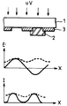
제1a도 내지 제1c도는 전술 인용 논문에서 제안된 프레넬 회절을 억제하는 원리를 보인 도이다.1A to 1C show the principle of suppressing Fresnel diffraction proposed in the above-cited papers.
제1a도는 종래의 레티클을 사용한 노광 시스템을 보인 것인데, 원하는 반도체 패턴에 따라 UV1표기된 자외선 광을 선택적으로 차단하는 크롬등의 불투명한 패턴(3)이 유리기재(1)에 제공되어 있다. 또한 위상 이동 패턴(2)에 의해 그 위상이 수정되지 않은 레티클을 투과한 자외선 광에 관하여, 투과되는 자외선 광의 위상을 이동시키기 위한 위상 이동 패턴(2)이 한쌍의 인접한 불투명 패턴(3) 사이에 제공된다.1A shows an exposure system using a conventional reticle, wherein an
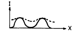
제1b도는 레티클을 투과한 광선 빔의 전형적인 전계(E) 분포를 나타낸 도이고 제1c도는 대응되는 광선 빔의 세기의 분포를 보인 도로 여기에서, 실선은 위상 이동 패턴이 제공된 경우를 나타내고 점선은 위상 이동 패턴이 제공되지 않은 경우를 나타낸다. 제1b도 및 제1c도에서 알 수 있는 바와 같이, 위상 이동 패턴(2)이 제공되지 않은 때 전달된 광선 빔은 광선의 회절로 인하여 불투명한 패턴(3)의 바로 아래의 영역에서 조차도 유한한 강도를 갖는다. 한편, 위상 이동 패턴(2)이 제공된때는 패턴(2)을 투과한 광선 빔의 위상을 그 위상이 이동되지 않고 레티클을 통과한 광선 빔에 관하여 반대로 될 수 있다.FIG. 1b shows a typical electric field (E) distribution of the beam of light passing through the reticle, and FIG. 1c shows a distribution of the intensity of the corresponding beam of beams, where the solid line shows the case where a phase shift pattern is provided and the dotted line shows the phase The case where no movement pattern is provided. As can be seen in FIGS. 1b and 1c, the transmitted beam of light when the phase shift pattern 2 is not provided is finite even in the region just below the
그러므로, 제1b도에서 실선으로 도시된 바와 같은 불투명한 패턴에 대응되는 전계 분포에는 음의 전계가 나타나며, 제1c도에서 실선으로 도시된 바와 같은 날카롭게 한정된 고해상도의 패턴이 웨이퍼상에 투영된다.Therefore, a negative electric field appears in the electric field distribution corresponding to the opaque pattern as shown by the solid line in FIG. 1b, and a sharply defined high resolution pattern as shown by the solid line in FIG. 1c is projected onto the wafer.
종래에는 산화 규소물 또는 유기 금속등과 같은 절연물질로 위상 이동 패턴(2)을 형성하였다. 전자 빔 리소그래피에 의해 이러한 패턴을 형성함에 있어서는, 제2도에 도시된 바와 같이 전자가 패턴(2)을 형성하는 절연막 뿐만 아니라 유기 레지스트(4)에도 축적되며, 전자 빔이 클롬 반발력으로 인하여 목표로 하는 지점으로부터 상쇄되는 문제점이 있었다. 이러한 문제점으로 인하여 종래의 레티클로는 만족할만한 고해상도를 얻을 수가 없었다.Conventionally, the phase shift pattern 2 is formed of an insulating material such as silicon oxide or organic metal. In forming such a pattern by electron beam lithography, as shown in FIG. 2, electrons are accumulated not only in the insulating film forming the pattern 2, but also in the organic resist 4, and the electron beam is targeted due to the chromium repulsive force. There was a problem offset from the point. Due to this problem, a satisfactory high resolution cannot be obtained with a conventional reticle.
따라서, 본 발명의 목적은 전술한 문제점들이 제거된 새롭고도 유용한 레티클을 제공하는데 있다.It is therefore an object of the present invention to provide a new and useful reticle in which the above-mentioned problems are eliminated.
본 발명의 다른 구체적인 목적은 제조공정중에 대전 입자 빔에 노출되더라도 전하의 충전을 유발시키지 않는 레티클을 제공하는데 있다.Another specific object of the present invention is to provide a reticle which does not cause charge of an electric charge even when exposed to a charged particle beam during the manufacturing process.
본 발명의 또다른 목적은 광학적으로 투명한 기재, 원하는 패턴이 형성되도록 입사되는 광선 빔을 차단하거나 투과시키도록 기판상에 형성되는 불투명한 패턴 및 투명 패턴을 통과하는 광선 빔에 대응하여 기재상에 제공되며 광선 빔의 위상을 이동시키기 위한 위상 이동패턴으로 이루어진 레티클을 제공하고자 하는 것으로 여기에서, 상기 위상 이동 패턴은 광학적으로 투명하고 전기적으로는 도전체인물질로 구성되어 있다. 본 발명에 따르면, 전자 빔 리소그래피와 같은 대전입자 빔 리소그래피에 의해 위상 이동 패턴을 패터닝하는 공정은 패터닝에 사용되는 위상 이동 패턴이나 레지스트를 형성하는 재료의 충전을 유발시키지 않으며 따라서, 정밀한 위상 이동 패턴의 패터닝이 가능해진다. 따라서, 투영될 반도체 장치의 치수가 극도로 작을 때조차도 위상 이동패턴에 의해 회절을 효율적으로 상쇄시키게 된다.Another object of the present invention is to provide on a substrate corresponding to an optically transparent substrate, an opaque pattern formed on the substrate to block or transmit an incident beam of light to form a desired pattern, and a beam of light passing through the transparent pattern. To provide a reticle consisting of a phase shift pattern for shifting the phase of the light beam, wherein the phase shift pattern is composed of an optically transparent and electrically conductive material. According to the present invention, the process of patterning the phase shift pattern by charged particle beam lithography, such as electron beam lithography, does not cause the phase shift pattern used for patterning or the filling of the material forming the resist, and thus the precise phase shift pattern Patterning becomes possible. Therefore, even when the dimensions of the semiconductor device to be projected are extremely small, the diffraction is effectively canceled by the phase shift pattern.
본 발명의 또다른 목적 및 특징들은 첨부된 도면에 의거한 이하의 설명으로부터 명백히 알 수 있을 것이다.Other objects and features of the present invention will become apparent from the following description based on the accompanying drawings.
제3a도 내지 제3g도는 본 발명의 실시예에 따른 레티클을 형성하는 공정을 보인 도이다.3A to 3G illustrate a process of forming a reticle according to an embodiment of the present invention.
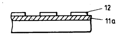
먼저 제3a도에서, 크롬 또는 크롬 산화물로 이루어진 불투명한 막(11a)이 1.5-2.0㎜의 전형적인 두께를 갖는 석영기재상에 증착된다. 이어, 레지스트(12a)가 불투명한 막(11a)상에 증착된다.First, in FIG. 3a, an
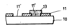
제3b도의 단계에서는, 원하는 반도체 패턴에 따라 전자 빔 노출 공정에 의해 레지스트(12a)가 패터닝된다. 다음에 제3c도의 단계에서는 불투명한 막(11a)이 패터닝된 레지스트(12a)를 마스크로하여 건식에칭 공정 또는 습식 에칭 공정에 의해 패터닝된다. 이렇게 하여 불투명한 레티클 패턴(11)이 소자 패턴에 상응하여 형성되며, 패턴(11)의 사이에는 투명한 영역(11' 및 11")이 남게 된다.In the step of FIG. 3B, the resist 12a is patterned by an electron beam exposure process in accordance with the desired semiconductor pattern. Next, in the step of FIG. 3C, the
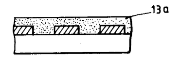
다음, 레지스트(12)가 제거된 후에 ITO 또는 주석 산화물(SnO2)로 더 잘알려진 인듐 주석 산화물(In2O3·SnO2)과 같은 투명하고 전기적으로 도전체인 물질로된 층(13a)이 제3c도에 도시된 레티클 패턴(11)을 덮도록 증착된다. 이 층(13a)은 다음의 관계식을 만족시키는 두께 α로 증착된다.Next, after the
α=λ/2(n-1)α = λ / 2 (n-1)
여기에서, λ는 웨이퍼상에 소자 패턴을 전사하는데 사용되는 자외선 또는 원자외선의 파장을 나타내며, n은 층(13a)의 반사 지수를 나타낸다. 여기에서 전술한 관계식이 만족될 때만이 제1a도 내지 제1c도에서 설명한 위상 이동 패턴에 의한 회절이 상쇄된다는 사실에 유의하자. 노광시에 사용되는 광선 빔의 파장이 0.4㎛이고 층(13a)의 반사 지수가 2라고 할때, 두께 α는 0.2㎛로 된다. 또한, 층(13a)이 도전막임을 유의할 필요가 있다.Here, lambda represents the wavelength of ultraviolet or far ultraviolet rays used to transfer the element pattern on the wafer, and n represents the reflection index of the
다음, 레지스트(14a)가 제3e도에 도시된 바와 같이 층(13a)상에 증착되고 이어 제3f도에 도시된 바와 같이 원하는 위상 이동 패턴이 형성되도록 레지스트(14a)가 전자 빔에 의해 패터닝된다. 이 공정에서, 전자 빔으로 레지스트(14)에 입사되는 전자는 곧 바로 도전층(13a)에서 접지를 통하여 빠져 나가게 되어 레지스트(14)나 층(13a)내에 남아있는 전자는 없게된다. 따라서, 레지스트(14a)를 패터닝하는데 사용되는 전자 빔이 레지스트(14a)를 정확하게 가격할 수 있게 된다. 이 공정에서 충전된 전하에 의한 전자 빔의 공전현상이 일어나지 않게 된다.Next, resist 14a is deposited on
다음에, 층(13a)은 패터닝된 레지스트(14)를 마스크로 하여 패터닝되어 제3g도에 도시된 바와 같이 원하는 위상 이동 패턴이 얻어진다. 제3g도에 도시된 바와 같이, 위상 이동 패턴(13)은 투명한 영역(11")에는 제공되지만 인접한 투명 영역(11")에는 제공되지 않는다. 이렇게 하여, 영역(11') 및 영역(11")를 통과한 자외선 빔의 회절에 대한 상쇄 현상이 제1a도 내지 제1c도에서 설명한 바와 같이 얻어진다.Next, the
층(13a)이 ITO로 이루어질때 제3g도의 단계에서의 패터닝은 CH4/H2의 혼합 가스를 5×10⁻³torr의 기압하에서 300W의 고주파 전력을 약 3-5분간 인가하여 건식 에칭하는 것에 의해 얻어진다. 건식 에칭중의 기재의 온도는 70℃로 설정된다. CH4의 대응으로는 부틸 아세테이트 또는 카본테트라클로라이드가 사용될 수 있다. 여기에서 전술한 바와 같은 필요 두께를 얻기 위해서는 그 기간이 조절되어야 함은 말할 것도없다.When the
한편, 층(13a)이 SnO2로 이루어질때, 40%의 부틸 아세테이트를 함유하는 수소 및 부틸 아세테이트의 혼합물이 사용될 수도 있다. 이 경우에는 기압을 약 10-3torr로 설정하고 200-500W의 고주파 전력을 약 1분동안 인가한다.On the other hand, when the
전술한 공정에 따르면, 위상 이동 패턴(13)이 매우 정밀하게 형성되어 회절을 효과적으로 상쇄시킬 수가 있다.According to the above-described process, the
또한 본 발명은 전술한 실시예로 제한되지는 않으며, 본 발명의 범위를 벗어나지 않는 한계내에서 다양하게 변형되거나 수정될 수 있다.In addition, the present invention is not limited to the above-described embodiments, and may be variously modified or modified within the limits without departing from the scope of the present invention.
Claims (6)
Applications Claiming Priority (2)
| Application Number | Priority Date | Filing Date | Title |
|---|---|---|---|
| JP02-20496 | 1990-02-01 | ||
| JP2020496A JPH03228053A (en) | 1990-02-01 | 1990-02-01 | Optical exposing reticule |
Publications (2)
| Publication Number | Publication Date |
|---|---|
| KR920000006A KR920000006A (en) | 1992-01-10 |
| KR940001552B1 true KR940001552B1 (en) | 1994-02-24 |
Family
ID=12028772
Family Applications (1)
| Application Number | Title | Priority Date | Filing Date |
|---|---|---|---|
| KR1019910001685A Expired - Fee Related KR940001552B1 (en) | 1990-02-01 | 1991-01-31 | Reticle for Photolithographic Patterning |
Country Status (5)
| Country | Link |
|---|---|
| US (1) | US5126220A (en) |
| EP (1) | EP0440467B1 (en) |
| JP (1) | JPH03228053A (en) |
| KR (1) | KR940001552B1 (en) |
| DE (1) | DE69115062T2 (en) |
Families Citing this family (23)
| Publication number | Priority date | Publication date | Assignee | Title |
|---|---|---|---|---|
| EP0773477B1 (en) * | 1990-09-21 | 2001-05-30 | Dai Nippon Printing Co., Ltd. | Process for producing a phase shift photomask |
| US5660956A (en) * | 1990-11-29 | 1997-08-26 | Kabushiki Kaisha Toshiba | Reticle and method of fabricating reticle |
| US5595844A (en) * | 1990-11-29 | 1997-01-21 | Kabushiki Kaisha Toshiba | Method of exposing light in a method of fabricating a reticle |
| JPH0567558A (en) * | 1991-09-06 | 1993-03-19 | Nikon Corp | Exposure method |
| JP2595149B2 (en) * | 1991-09-25 | 1997-03-26 | 株式会社日立製作所 | Electron beam drawing equipment |
| JP2874406B2 (en) * | 1991-10-09 | 1999-03-24 | 株式会社日立製作所 | Defect repair method for phase shifter mask |
| SG50543A1 (en) * | 1991-11-22 | 1998-07-20 | At & T Corp | Fabrication of phase-shifting lithographic masks |
| US5300786A (en) * | 1992-10-28 | 1994-04-05 | International Business Machines Corporation | Optical focus phase shift test pattern, monitoring system and process |
| US5376483A (en) * | 1993-10-07 | 1994-12-27 | Micron Semiconductor, Inc. | Method of making masks for phase shifting lithography |
| US5470681A (en) * | 1993-12-23 | 1995-11-28 | International Business Machines Corporation | Phase shift mask using liquid phase oxide deposition |
| US5495959A (en) * | 1994-05-11 | 1996-03-05 | Micron Technology, Inc. | Method of making substractive rim phase shifting masks |
| US5487962A (en) * | 1994-05-11 | 1996-01-30 | Rolfson; J. Brett | Method of chromeless phase shift mask fabrication suitable for auto-cad layout |
| US5414580A (en) * | 1994-05-13 | 1995-05-09 | International Business Machines Corporation | Magnetic storage system using thin film magnetic recording heads using phase-shifting mask |
| US5468578A (en) * | 1994-09-26 | 1995-11-21 | Micron Technology, Inc. | Method of making masks for phase shifting lithography to avoid phase conflicts |
| US5536606A (en) * | 1995-05-30 | 1996-07-16 | Micron Technology, Inc. | Method for making self-aligned rim phase shifting masks for sub-micron lithography |
| US5766829A (en) * | 1995-05-30 | 1998-06-16 | Micron Technology, Inc. | Method of phase shift lithography |
| KR100263034B1 (en) * | 1995-12-02 | 2000-08-01 | 김지태 | Intelligent safety |
| US6057587A (en) * | 1997-08-28 | 2000-05-02 | Vlsi Technology, Inc. | Semiconductor device with anti-reflective structure |
| KR20020021907A (en) * | 2000-09-18 | 2002-03-23 | 신형인 | Rubber composition for tire improved fatigue properties |
| US6859997B1 (en) | 2000-09-19 | 2005-03-01 | Western Digital (Fremont), Inc. | Method for manufacturing a magnetic write element |
| DE10228546B4 (en) * | 2002-06-26 | 2006-08-10 | Infineon Technologies Ag | Process for structuring a lithography mask |
| JP5270142B2 (en) * | 2007-12-05 | 2013-08-21 | 浜松ホトニクス株式会社 | Reflective spatial light modulator |
| SE1550411A1 (en) * | 2015-04-07 | 2016-10-08 | Fingerprint Cards Ab | Electronic device comprising fingerprint sensor |
Family Cites Families (4)
| Publication number | Priority date | Publication date | Assignee | Title |
|---|---|---|---|---|
| DE3374452D1 (en) * | 1982-04-05 | 1987-12-17 | Ibm | Method of increasing the image resolution of a transmitting mask and improved masks for performing the method |
| JPS61128251A (en) * | 1984-11-26 | 1986-06-16 | Mitsubishi Electric Corp | X-ray exposure mask |
| JPH0682604B2 (en) * | 1987-08-04 | 1994-10-19 | 三菱電機株式会社 | X-ray mask |
| JP2710967B2 (en) * | 1988-11-22 | 1998-02-10 | 株式会社日立製作所 | Manufacturing method of integrated circuit device |
-
1990
- 1990-02-01 JP JP2020496A patent/JPH03228053A/en active Pending
-
1991
- 1991-01-31 DE DE69115062T patent/DE69115062T2/en not_active Expired - Fee Related
- 1991-01-31 US US07/648,697 patent/US5126220A/en not_active Expired - Lifetime
- 1991-01-31 KR KR1019910001685A patent/KR940001552B1/en not_active Expired - Fee Related
- 1991-01-31 EP EP91300753A patent/EP0440467B1/en not_active Expired - Lifetime
Also Published As
| Publication number | Publication date |
|---|---|
| DE69115062D1 (en) | 1996-01-18 |
| DE69115062T2 (en) | 1996-05-09 |
| US5126220A (en) | 1992-06-30 |
| JPH03228053A (en) | 1991-10-09 |
| EP0440467A2 (en) | 1991-08-07 |
| EP0440467A3 (en) | 1991-10-30 |
| KR920000006A (en) | 1992-01-10 |
| EP0440467B1 (en) | 1995-12-06 |
Similar Documents
| Publication | Publication Date | Title |
|---|---|---|
| KR940001552B1 (en) | Reticle for Photolithographic Patterning | |
| US5275896A (en) | Single-alignment-level lithographic technique for achieving self-aligned features | |
| JP3105234B2 (en) | Method for manufacturing semiconductor device | |
| EP0577297B1 (en) | Self-aligned method of making phase-shifting lithographic masks having three or more phase-shifts | |
| US5405721A (en) | Phase-shifting lithographic masks having phase-shifting layers of differing compositions | |
| KR100190358B1 (en) | Phase mask for photolithographic projection and process for its preparation | |
| US5244759A (en) | Single-alignment-level lithographic technique for achieving self-aligned features | |
| EP0475694B1 (en) | Optical mask using phase shift and method of producing the same | |
| US3758326A (en) | Mask or original for reproducing patterns on light sensitive layers | |
| US5300378A (en) | Method of producing a phase shifting mask | |
| JP2641362B2 (en) | Lithography method and manufacturing method of phase shift mask | |
| KR0135149B1 (en) | Manufacturing method of phase inversion mask | |
| US5468576A (en) | Method for manufacturing exposure mask | |
| KR950007477B1 (en) | Phase inversion mask and manufacturing method thereof | |
| JP2652341B2 (en) | Method for manufacturing phase inversion mask | |
| CN112925164A (en) | Photomask plate and forming method thereof | |
| JP2783582B2 (en) | Photo mask | |
| JP4099836B2 (en) | Halftone phase shift mask blank, method of manufacturing the same, and halftone phase shift mask | |
| JPH07281414A (en) | Phase shift mask blank, phase shift mask and manufacturing method thereof | |
| KR0151228B1 (en) | Photomask for preparing resist pattern | |
| KR100790565B1 (en) | Photo mask | |
| KR19990050484A (en) | Method for manufacturing half-tone phase reversal mask | |
| JP2739008B2 (en) | Phase shift mask and method of manufacturing the same | |
| KR940011095B1 (en) | Phase shift mask, pattern building method using the same | |
| JP2913753B2 (en) | Method for manufacturing phase shift mask |
Legal Events
| Date | Code | Title | Description |
|---|---|---|---|
| A201 | Request for examination | ||
| PA0109 | Patent application |
St.27 status event code: A-0-1-A10-A12-nap-PA0109 |
|
| PA0201 | Request for examination |
St.27 status event code: A-1-2-D10-D11-exm-PA0201 |
|
| R17-X000 | Change to representative recorded |
St.27 status event code: A-3-3-R10-R17-oth-X000 |
|
| PG1501 | Laying open of application |
St.27 status event code: A-1-1-Q10-Q12-nap-PG1501 |
|
| G160 | Decision to publish patent application | ||
| PG1605 | Publication of application before grant of patent |
St.27 status event code: A-2-2-Q10-Q13-nap-PG1605 |
|
| E701 | Decision to grant or registration of patent right | ||
| PE0701 | Decision of registration |
St.27 status event code: A-1-2-D10-D22-exm-PE0701 |
|
| GRNT | Written decision to grant | ||
| PR0701 | Registration of establishment |
St.27 status event code: A-2-4-F10-F11-exm-PR0701 |
|
| PR1002 | Payment of registration fee |
St.27 status event code: A-2-2-U10-U11-oth-PR1002 Fee payment year number: 1 |
|
| PR1001 | Payment of annual fee |
St.27 status event code: A-4-4-U10-U11-oth-PR1001 Fee payment year number: 4 |
|
| PR1001 | Payment of annual fee |
St.27 status event code: A-4-4-U10-U11-oth-PR1001 Fee payment year number: 5 |
|
| PN2301 | Change of applicant |
St.27 status event code: A-5-5-R10-R13-asn-PN2301 St.27 status event code: A-5-5-R10-R11-asn-PN2301 |
|
| PN2301 | Change of applicant |
St.27 status event code: A-5-5-R10-R13-asn-PN2301 St.27 status event code: A-5-5-R10-R11-asn-PN2301 |
|
| PR1001 | Payment of annual fee |
St.27 status event code: A-4-4-U10-U11-oth-PR1001 Fee payment year number: 6 |
|
| R18-X000 | Changes to party contact information recorded |
St.27 status event code: A-5-5-R10-R18-oth-X000 |
|
| R18-X000 | Changes to party contact information recorded |
St.27 status event code: A-5-5-R10-R18-oth-X000 |
|
| PR1001 | Payment of annual fee |
St.27 status event code: A-4-4-U10-U11-oth-PR1001 Fee payment year number: 7 |
|
| PN2301 | Change of applicant |
St.27 status event code: A-5-5-R10-R13-asn-PN2301 St.27 status event code: A-5-5-R10-R11-asn-PN2301 |
|
| PR1001 | Payment of annual fee |
St.27 status event code: A-4-4-U10-U11-oth-PR1001 Fee payment year number: 8 |
|
| PR1001 | Payment of annual fee |
St.27 status event code: A-4-4-U10-U11-oth-PR1001 Fee payment year number: 9 |
|
| PR1001 | Payment of annual fee |
St.27 status event code: A-4-4-U10-U11-oth-PR1001 Fee payment year number: 10 |
|
| FPAY | Annual fee payment |
Payment date: 20040205 Year of fee payment: 11 |
|
| PR1001 | Payment of annual fee |
St.27 status event code: A-4-4-U10-U11-oth-PR1001 Fee payment year number: 11 |
|
| LAPS | Lapse due to unpaid annual fee | ||
| PC1903 | Unpaid annual fee |
St.27 status event code: A-4-4-U10-U13-oth-PC1903 Not in force date: 20050225 Payment event data comment text: Termination Category : DEFAULT_OF_REGISTRATION_FEE |
|
| PC1903 | Unpaid annual fee |
St.27 status event code: N-4-6-H10-H13-oth-PC1903 Ip right cessation event data comment text: Termination Category : DEFAULT_OF_REGISTRATION_FEE Not in force date: 20050225 |
|
| P22-X000 | Classification modified |
St.27 status event code: A-4-4-P10-P22-nap-X000 |