KR20240037964A - 광 검출 장치 및 그 제조 방법 그리고 전자 기기 - Google Patents
광 검출 장치 및 그 제조 방법 그리고 전자 기기 Download PDFInfo
- Publication number
- KR20240037964A KR20240037964A KR1020247002185A KR20247002185A KR20240037964A KR 20240037964 A KR20240037964 A KR 20240037964A KR 1020247002185 A KR1020247002185 A KR 1020247002185A KR 20247002185 A KR20247002185 A KR 20247002185A KR 20240037964 A KR20240037964 A KR 20240037964A
- Authority
- KR
- South Korea
- Prior art keywords
- film
- light
- filler
- semiconductor layer
- oxide
- Prior art date
- Legal status (The legal status is an assumption and is not a legal conclusion. Google has not performed a legal analysis and makes no representation as to the accuracy of the status listed.)
- Pending
Links
Images


















































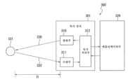
Classifications
-
- G—PHYSICS
- G02—OPTICS
- G02B—OPTICAL ELEMENTS, SYSTEMS OR APPARATUS
- G02B1/00—Optical elements characterised by the material of which they are made; Optical coatings for optical elements
- G02B1/10—Optical coatings produced by application to, or surface treatment of, optical elements
- G02B1/11—Anti-reflection coatings
-
- H01L27/14625—
-
- H—ELECTRICITY
- H10—SEMICONDUCTOR DEVICES; ELECTRIC SOLID-STATE DEVICES NOT OTHERWISE PROVIDED FOR
- H10F—INORGANIC SEMICONDUCTOR DEVICES SENSITIVE TO INFRARED RADIATION, LIGHT, ELECTROMAGNETIC RADIATION OF SHORTER WAVELENGTH OR CORPUSCULAR RADIATION
- H10F39/00—Integrated devices, or assemblies of multiple devices, comprising at least one element covered by group H10F30/00, e.g. radiation detectors comprising photodiode arrays
- H10F39/80—Constructional details of image sensors
- H10F39/806—Optical elements or arrangements associated with the image sensors
-
- H—ELECTRICITY
- H10—SEMICONDUCTOR DEVICES; ELECTRIC SOLID-STATE DEVICES NOT OTHERWISE PROVIDED FOR
- H10F—INORGANIC SEMICONDUCTOR DEVICES SENSITIVE TO INFRARED RADIATION, LIGHT, ELECTROMAGNETIC RADIATION OF SHORTER WAVELENGTH OR CORPUSCULAR RADIATION
- H10F39/00—Integrated devices, or assemblies of multiple devices, comprising at least one element covered by group H10F30/00, e.g. radiation detectors comprising photodiode arrays
- H10F39/80—Constructional details of image sensors
- H10F39/805—Coatings
-
- G—PHYSICS
- G02—OPTICS
- G02B—OPTICAL ELEMENTS, SYSTEMS OR APPARATUS
- G02B1/00—Optical elements characterised by the material of which they are made; Optical coatings for optical elements
- G02B1/002—Optical elements characterised by the material of which they are made; Optical coatings for optical elements made of materials engineered to provide properties not available in nature, e.g. metamaterials
-
- G—PHYSICS
- G02—OPTICS
- G02B—OPTICAL ELEMENTS, SYSTEMS OR APPARATUS
- G02B5/00—Optical elements other than lenses
-
- G—PHYSICS
- G02—OPTICS
- G02B—OPTICAL ELEMENTS, SYSTEMS OR APPARATUS
- G02B5/00—Optical elements other than lenses
- G02B5/30—Polarising elements
-
- H01L27/14603—
-
- H01L27/1462—
-
- H01L27/14685—
-
- H—ELECTRICITY
- H10—SEMICONDUCTOR DEVICES; ELECTRIC SOLID-STATE DEVICES NOT OTHERWISE PROVIDED FOR
- H10F—INORGANIC SEMICONDUCTOR DEVICES SENSITIVE TO INFRARED RADIATION, LIGHT, ELECTROMAGNETIC RADIATION OF SHORTER WAVELENGTH OR CORPUSCULAR RADIATION
- H10F30/00—Individual radiation-sensitive semiconductor devices in which radiation controls the flow of current through the devices, e.g. photodetectors
- H10F30/20—Individual radiation-sensitive semiconductor devices in which radiation controls the flow of current through the devices, e.g. photodetectors the devices having potential barriers, e.g. phototransistors
-
- H—ELECTRICITY
- H10—SEMICONDUCTOR DEVICES; ELECTRIC SOLID-STATE DEVICES NOT OTHERWISE PROVIDED FOR
- H10F—INORGANIC SEMICONDUCTOR DEVICES SENSITIVE TO INFRARED RADIATION, LIGHT, ELECTROMAGNETIC RADIATION OF SHORTER WAVELENGTH OR CORPUSCULAR RADIATION
- H10F39/00—Integrated devices, or assemblies of multiple devices, comprising at least one element covered by group H10F30/00, e.g. radiation detectors comprising photodiode arrays
- H10F39/011—Manufacture or treatment of image sensors covered by group H10F39/12
- H10F39/014—Manufacture or treatment of image sensors covered by group H10F39/12 of CMOS image sensors
-
- H—ELECTRICITY
- H10—SEMICONDUCTOR DEVICES; ELECTRIC SOLID-STATE DEVICES NOT OTHERWISE PROVIDED FOR
- H10F—INORGANIC SEMICONDUCTOR DEVICES SENSITIVE TO INFRARED RADIATION, LIGHT, ELECTROMAGNETIC RADIATION OF SHORTER WAVELENGTH OR CORPUSCULAR RADIATION
- H10F39/00—Integrated devices, or assemblies of multiple devices, comprising at least one element covered by group H10F30/00, e.g. radiation detectors comprising photodiode arrays
- H10F39/011—Manufacture or treatment of image sensors covered by group H10F39/12
- H10F39/024—Manufacture or treatment of image sensors covered by group H10F39/12 of coatings or optical elements
-
- H—ELECTRICITY
- H10—SEMICONDUCTOR DEVICES; ELECTRIC SOLID-STATE DEVICES NOT OTHERWISE PROVIDED FOR
- H10F—INORGANIC SEMICONDUCTOR DEVICES SENSITIVE TO INFRARED RADIATION, LIGHT, ELECTROMAGNETIC RADIATION OF SHORTER WAVELENGTH OR CORPUSCULAR RADIATION
- H10F39/00—Integrated devices, or assemblies of multiple devices, comprising at least one element covered by group H10F30/00, e.g. radiation detectors comprising photodiode arrays
- H10F39/10—Integrated devices
- H10F39/12—Image sensors
- H10F39/18—Complementary metal-oxide-semiconductor [CMOS] image sensors; Photodiode array image sensors
- H10F39/184—Infrared image sensors
-
- H—ELECTRICITY
- H10—SEMICONDUCTOR DEVICES; ELECTRIC SOLID-STATE DEVICES NOT OTHERWISE PROVIDED FOR
- H10F—INORGANIC SEMICONDUCTOR DEVICES SENSITIVE TO INFRARED RADIATION, LIGHT, ELECTROMAGNETIC RADIATION OF SHORTER WAVELENGTH OR CORPUSCULAR RADIATION
- H10F39/00—Integrated devices, or assemblies of multiple devices, comprising at least one element covered by group H10F30/00, e.g. radiation detectors comprising photodiode arrays
- H10F39/80—Constructional details of image sensors
- H10F39/802—Geometry or disposition of elements in pixels, e.g. address-lines or gate electrodes
-
- H—ELECTRICITY
- H10—SEMICONDUCTOR DEVICES; ELECTRIC SOLID-STATE DEVICES NOT OTHERWISE PROVIDED FOR
- H10F—INORGANIC SEMICONDUCTOR DEVICES SENSITIVE TO INFRARED RADIATION, LIGHT, ELECTROMAGNETIC RADIATION OF SHORTER WAVELENGTH OR CORPUSCULAR RADIATION
- H10F39/00—Integrated devices, or assemblies of multiple devices, comprising at least one element covered by group H10F30/00, e.g. radiation detectors comprising photodiode arrays
- H10F39/80—Constructional details of image sensors
- H10F39/806—Optical elements or arrangements associated with the image sensors
- H10F39/8063—Microlenses
-
- H—ELECTRICITY
- H10—SEMICONDUCTOR DEVICES; ELECTRIC SOLID-STATE DEVICES NOT OTHERWISE PROVIDED FOR
- H10F—INORGANIC SEMICONDUCTOR DEVICES SENSITIVE TO INFRARED RADIATION, LIGHT, ELECTROMAGNETIC RADIATION OF SHORTER WAVELENGTH OR CORPUSCULAR RADIATION
- H10F39/00—Integrated devices, or assemblies of multiple devices, comprising at least one element covered by group H10F30/00, e.g. radiation detectors comprising photodiode arrays
- H10F39/80—Constructional details of image sensors
- H10F39/806—Optical elements or arrangements associated with the image sensors
- H10F39/8067—Reflectors
-
- H—ELECTRICITY
- H10—SEMICONDUCTOR DEVICES; ELECTRIC SOLID-STATE DEVICES NOT OTHERWISE PROVIDED FOR
- H10F—INORGANIC SEMICONDUCTOR DEVICES SENSITIVE TO INFRARED RADIATION, LIGHT, ELECTROMAGNETIC RADIATION OF SHORTER WAVELENGTH OR CORPUSCULAR RADIATION
- H10F77/00—Constructional details of devices covered by this subclass
- H10F77/40—Optical elements or arrangements
-
- H—ELECTRICITY
- H10—SEMICONDUCTOR DEVICES; ELECTRIC SOLID-STATE DEVICES NOT OTHERWISE PROVIDED FOR
- H10F—INORGANIC SEMICONDUCTOR DEVICES SENSITIVE TO INFRARED RADIATION, LIGHT, ELECTROMAGNETIC RADIATION OF SHORTER WAVELENGTH OR CORPUSCULAR RADIATION
- H10F77/00—Constructional details of devices covered by this subclass
- H10F77/40—Optical elements or arrangements
- H10F77/413—Optical elements or arrangements directly associated or integrated with the devices, e.g. back reflectors
Landscapes
- Physics & Mathematics (AREA)
- General Physics & Mathematics (AREA)
- Optics & Photonics (AREA)
- Solid State Image Pick-Up Elements (AREA)
Applications Claiming Priority (3)
| Application Number | Priority Date | Filing Date | Title |
|---|---|---|---|
| JPJP-P-2021-130077 | 2021-08-06 | ||
| JP2021130077 | 2021-08-06 | ||
| PCT/JP2022/029175 WO2023013521A1 (ja) | 2021-08-06 | 2022-07-28 | 光検出装置及びその製造方法並びに電子機器 |
Publications (1)
| Publication Number | Publication Date |
|---|---|
| KR20240037964A true KR20240037964A (ko) | 2024-03-22 |
Family
ID=85154528
Family Applications (1)
| Application Number | Title | Priority Date | Filing Date |
|---|---|---|---|
| KR1020247002185A Pending KR20240037964A (ko) | 2021-08-06 | 2022-07-28 | 광 검출 장치 및 그 제조 방법 그리고 전자 기기 |
Country Status (7)
| Country | Link |
|---|---|
| US (1) | US20250120205A1 (https=) |
| EP (1) | EP4383333A4 (https=) |
| JP (1) | JPWO2023013521A1 (https=) |
| KR (1) | KR20240037964A (https=) |
| CN (1) | CN117678073A (https=) |
| TW (1) | TW202310382A (https=) |
| WO (1) | WO2023013521A1 (https=) |
Families Citing this family (24)
| Publication number | Priority date | Publication date | Assignee | Title |
|---|---|---|---|---|
| CN114873556B (zh) * | 2022-05-16 | 2025-07-04 | 苏州山河光电科技有限公司 | 一种超表面光学元件的制作方法 |
| CN217386086U (zh) * | 2022-05-25 | 2022-09-06 | 天津山河光电科技有限公司 | 感光组件、成像系统及光学电子设备 |
| CN115327678B (zh) * | 2022-09-01 | 2024-11-22 | 天津山河光电科技有限公司 | 双向光路系统、光学模组及光学设备 |
| JPWO2024161881A1 (https=) * | 2023-01-31 | 2024-08-08 | ||
| US20240322056A1 (en) * | 2023-03-21 | 2024-09-26 | Visera Technologies Company Ltd. | Optical device |
| TW202447946A (zh) * | 2023-04-28 | 2024-12-01 | 日商索尼半導體解決方案公司 | 攝像裝置及電子機器 |
| JP2024164446A (ja) * | 2023-05-15 | 2024-11-27 | ソニーセミコンダクタソリューションズ株式会社 | 光検出装置および電子機器 |
| JP2025009510A (ja) * | 2023-07-07 | 2025-01-20 | ソニーグループ株式会社 | 光検出装置 |
| JP2025016280A (ja) * | 2023-07-21 | 2025-01-31 | ソニーセミコンダクタソリューションズ株式会社 | 光検出装置 |
| WO2025121000A1 (ja) * | 2023-12-07 | 2025-06-12 | ソニーセミコンダクタソリューションズ株式会社 | 光検出装置 |
| WO2025121422A1 (ja) * | 2023-12-07 | 2025-06-12 | ソニーセミコンダクタソリューションズ株式会社 | 光検出装置 |
| WO2025158986A1 (ja) * | 2024-01-24 | 2025-07-31 | パナソニックIpマネジメント株式会社 | 光学素子 |
| WO2025158987A1 (ja) * | 2024-01-24 | 2025-07-31 | パナソニックIpマネジメント株式会社 | 光学素子 |
| WO2025164103A1 (ja) * | 2024-01-31 | 2025-08-07 | ソニーセミコンダクタソリューションズ株式会社 | 光検出装置、光学素子、および電子機器 |
| WO2025182567A1 (ja) * | 2024-02-26 | 2025-09-04 | ソニーグループ株式会社 | 光検出装置および光検出システム |
| WO2025192164A1 (ja) * | 2024-03-15 | 2025-09-18 | ソニーセミコンダクタソリューションズ株式会社 | 光検出装置および電子機器 |
| WO2025204244A1 (ja) * | 2024-03-27 | 2025-10-02 | ソニーセミコンダクタソリューションズ株式会社 | 光検出装置、光検出装置の製造方法、および電子機器 |
| WO2025224901A1 (ja) * | 2024-04-24 | 2025-10-30 | ソニーセミコンダクタソリューションズ株式会社 | 光検出装置 |
| JP2025170719A (ja) * | 2024-05-07 | 2025-11-19 | キヤノン株式会社 | 光学素子、光学系、および撮像装置 |
| WO2025253793A1 (ja) * | 2024-06-07 | 2025-12-11 | ソニーセミコンダクタソリューションズ株式会社 | 光検出装置および電子機器 |
| WO2025258003A1 (ja) * | 2024-06-12 | 2025-12-18 | Ntt株式会社 | 光学素子 |
| WO2025263193A1 (ja) * | 2024-06-20 | 2025-12-26 | ソニーセミコンダクタソリューションズ株式会社 | 光検出装置 |
| WO2026048314A1 (ja) * | 2024-08-30 | 2026-03-05 | ソニーセミコンダクタソリューションズ株式会社 | 光学素子、光検出装置、および電子機器 |
| CN121646024A (zh) * | 2024-09-04 | 2026-03-10 | 华为技术有限公司 | 图像传感器及其制备方法、摄像头模组、电子设备 |
Citations (1)
| Publication number | Priority date | Publication date | Assignee | Title |
|---|---|---|---|---|
| WO2019046827A1 (en) | 2017-08-31 | 2019-03-07 | Metalenz, Inc. | INTEGRATION OF TRANSMISSIVE METASURFACE LENS |
Family Cites Families (14)
| Publication number | Priority date | Publication date | Assignee | Title |
|---|---|---|---|---|
| EP1785750A1 (en) * | 2004-09-01 | 2007-05-16 | Matsushita Electric Industrial Co., Ltd. | Condensing element, solid-state imaging device and method for fabricating the same |
| JP2008066702A (ja) * | 2006-08-10 | 2008-03-21 | Matsushita Electric Ind Co Ltd | 固体撮像素子及びカメラ |
| JP2011040441A (ja) * | 2009-08-06 | 2011-02-24 | Panasonic Corp | 固体撮像装置 |
| JP5197823B2 (ja) * | 2011-02-09 | 2013-05-15 | キヤノン株式会社 | 光電変換装置 |
| JP2015028960A (ja) * | 2011-12-01 | 2015-02-12 | ソニー株式会社 | 固体撮像装置および電子機器 |
| CN104698672B (zh) * | 2015-03-03 | 2019-04-09 | 厦门天马微电子有限公司 | 滤色片及其制备方法 |
| US10403668B2 (en) * | 2015-07-29 | 2019-09-03 | Samsung Electronics Co., Ltd. | Imaging apparatus and image sensor including the same |
| JP7166928B2 (ja) * | 2016-11-21 | 2022-11-08 | ソニーセミコンダクタソリューションズ株式会社 | 固体撮像素子、製造方法 |
| JP2018098641A (ja) | 2016-12-13 | 2018-06-21 | ソニーセミコンダクタソリューションズ株式会社 | 画像処理装置、画像処理方法、プログラム、および電子機器 |
| JP6987529B2 (ja) | 2017-05-15 | 2022-01-05 | ソニーセミコンダクタソリューションズ株式会社 | 撮像素子、撮像素子の製造方法、電子機器、及び、撮像モジュール |
| JPWO2018230186A1 (ja) * | 2017-06-15 | 2020-04-16 | 株式会社ニコン | 撮像素子、撮像装置および撮像方法 |
| CN111357112B (zh) * | 2017-12-22 | 2024-06-18 | 索尼半导体解决方案公司 | 固态成像装置和电子装置 |
| US11158661B2 (en) * | 2019-09-19 | 2021-10-26 | Omnivision Technologies, Inc. | Image sensor with micro-structured color filter |
| TWI725765B (zh) * | 2020-03-10 | 2021-04-21 | 力晶積成電子製造股份有限公司 | 具有表面微柱體結構的固態影像感測器暨其製作方法 |
-
2022
- 2022-06-30 TW TW111124464A patent/TW202310382A/zh unknown
- 2022-07-28 CN CN202280050388.9A patent/CN117678073A/zh active Pending
- 2022-07-28 WO PCT/JP2022/029175 patent/WO2023013521A1/ja not_active Ceased
- 2022-07-28 US US18/293,437 patent/US20250120205A1/en active Pending
- 2022-07-28 KR KR1020247002185A patent/KR20240037964A/ko active Pending
- 2022-07-28 EP EP22852943.4A patent/EP4383333A4/en active Pending
- 2022-07-28 JP JP2023540303A patent/JPWO2023013521A1/ja active Pending
Patent Citations (2)
| Publication number | Priority date | Publication date | Assignee | Title |
|---|---|---|---|---|
| WO2019046827A1 (en) | 2017-08-31 | 2019-03-07 | Metalenz, Inc. | INTEGRATION OF TRANSMISSIVE METASURFACE LENS |
| JP2020537193A (ja) | 2017-08-31 | 2020-12-17 | メタレンズ,インコーポレイテッド | 透過型メタサーフェスレンズ統合 |
Also Published As
| Publication number | Publication date |
|---|---|
| WO2023013521A1 (ja) | 2023-02-09 |
| JPWO2023013521A1 (https=) | 2023-02-09 |
| CN117678073A (zh) | 2024-03-08 |
| EP4383333A1 (en) | 2024-06-12 |
| TW202310382A (zh) | 2023-03-01 |
| EP4383333A4 (en) | 2024-10-23 |
| US20250120205A1 (en) | 2025-04-10 |
Similar Documents
| Publication | Publication Date | Title |
|---|---|---|
| KR20240037964A (ko) | 광 검출 장치 및 그 제조 방법 그리고 전자 기기 | |
| EP2320462B1 (en) | Image sensor having waveguides formed in color filters | |
| JP5538811B2 (ja) | 固体撮像素子 | |
| KR20240037970A (ko) | 광 검출기, 광 검출기의 제조 방법 및 전자 기기 | |
| TWI410129B (zh) | 固態攝影裝置以及其設計方法 | |
| US8669632B2 (en) | Solid-state imaging device and method for manufacturing the same | |
| CN116034480A (zh) | 成像装置和电子装置 | |
| JP6021439B2 (ja) | 固体撮像装置 | |
| CN108369949B (zh) | 固态成像元件、成像设备和用于制造固态成像元件的方法 | |
| KR20190035564A (ko) | 반도체 이미지 센서 | |
| CN114556573B (zh) | 图像传感器和成像装置 | |
| JP2009194340A (ja) | 光電変換装置、及び光電変換装置の製造方法 | |
| WO2024029383A1 (ja) | 光検出装置及び電子機器 | |
| US20150179692A1 (en) | Solid-state imaging apparatus and method of manufacturing the same | |
| JP7598975B2 (ja) | イメージセンサおよび画像信号処理装置の簡素化方法 | |
| CN116636018A (zh) | 固态成像装置 | |
| JP2013214616A (ja) | 固体撮像装置、固体撮像装置の製造方法及び電子機器 | |
| JP6465839B2 (ja) | 光電変換装置、撮像システム、移動体、および、光電変換装置の製造方法 | |
| JP2013038383A (ja) | 固体撮像素子、固体撮像素子の製造方法、および電子機器 | |
| TW201507119A (zh) | 固態影像感測裝置及固態影像感測裝置之製造方法 | |
| JP2016225324A (ja) | 固体撮像装置 | |
| US8581313B2 (en) | Solid-state imaging device | |
| JP5040088B2 (ja) | 固体撮像素子 | |
| JP5332823B2 (ja) | 固体撮像素子、撮像装置 | |
| US20260059899A1 (en) | Photodetector |
Legal Events
| Date | Code | Title | Description |
|---|---|---|---|
| PA0105 | International application |
St.27 status event code: A-0-1-A10-A15-nap-PA0105 |
|
| PG1501 | Laying open of application |
St.27 status event code: A-1-1-Q10-Q12-nap-PG1501 |
|
| P22-X000 | Classification modified |
St.27 status event code: A-2-2-P10-P22-nap-X000 |
|
| A201 | Request for examination | ||
| PA0201 | Request for examination |
St.27 status event code: A-1-2-D10-D11-exm-PA0201 |
|
| D13 | Search requested |
Free format text: ST27 STATUS EVENT CODE: A-1-2-D10-D13-SRH-X000 (AS PROVIDED BY THE NATIONAL OFFICE) |
|
| D13-X000 | Search requested |
St.27 status event code: A-1-2-D10-D13-srh-X000 |
|
| D21 | Rejection of application intended |
Free format text: ST27 STATUS EVENT CODE: A-1-2-D10-D21-EXM-PE0902 (AS PROVIDED BY THE NATIONAL OFFICE) |
|
| PE0902 | Notice of grounds for rejection |
St.27 status event code: A-1-2-D10-D21-exm-PE0902 |