KR20240037964A - Light detection device, manufacturing method and electronic device - Google Patents
Light detection device, manufacturing method and electronic device Download PDFInfo
- Publication number
- KR20240037964A KR20240037964A KR1020247002185A KR20247002185A KR20240037964A KR 20240037964 A KR20240037964 A KR 20240037964A KR 1020247002185 A KR1020247002185 A KR 1020247002185A KR 20247002185 A KR20247002185 A KR 20247002185A KR 20240037964 A KR20240037964 A KR 20240037964A
- Authority
- KR
- South Korea
- Prior art keywords
- film
- light
- filler
- semiconductor layer
- oxide
- Prior art date
Links
- 238000001514 detection method Methods 0.000 title claims abstract description 77
- 238000004519 manufacturing process Methods 0.000 title claims description 85
- 239000000945 filler Substances 0.000 claims abstract description 265
- 239000004065 semiconductor Substances 0.000 claims abstract description 235
- 238000006243 chemical reaction Methods 0.000 claims abstract description 71
- 238000000034 method Methods 0.000 claims description 278
- 238000003384 imaging method Methods 0.000 claims description 182
- 239000012780 transparent material Substances 0.000 claims description 95
- 239000000463 material Substances 0.000 claims description 75
- 229910052581 Si3N4 Inorganic materials 0.000 claims description 71
- HQVNEWCFYHHQES-UHFFFAOYSA-N silicon nitride Chemical compound N12[Si]34N5[Si]62N3[Si]51N64 HQVNEWCFYHHQES-UHFFFAOYSA-N 0.000 claims description 71
- 230000001681 protective effect Effects 0.000 claims description 68
- 238000012545 processing Methods 0.000 claims description 63
- 229910052814 silicon oxide Inorganic materials 0.000 claims description 52
- VYPSYNLAJGMNEJ-UHFFFAOYSA-N Silicium dioxide Chemical compound O=[Si]=O VYPSYNLAJGMNEJ-UHFFFAOYSA-N 0.000 claims description 46
- 238000005530 etching Methods 0.000 claims description 45
- 230000003014 reinforcing effect Effects 0.000 claims description 39
- 230000003287 optical effect Effects 0.000 claims description 31
- HBMJWWWQQXIZIP-UHFFFAOYSA-N silicon carbide Chemical compound [Si+]#[C-] HBMJWWWQQXIZIP-UHFFFAOYSA-N 0.000 claims description 28
- 229910010271 silicon carbide Inorganic materials 0.000 claims description 28
- 229910021417 amorphous silicon Inorganic materials 0.000 claims description 26
- 230000002787 reinforcement Effects 0.000 claims description 25
- 239000011347 resin Substances 0.000 claims description 25
- 229920005989 resin Polymers 0.000 claims description 25
- PPBRXRYQALVLMV-UHFFFAOYSA-N Styrene Chemical compound C=CC1=CC=CC=C1 PPBRXRYQALVLMV-UHFFFAOYSA-N 0.000 claims description 20
- GWEVSGVZZGPLCZ-UHFFFAOYSA-N Titan oxide Chemical compound O=[Ti]=O GWEVSGVZZGPLCZ-UHFFFAOYSA-N 0.000 claims description 18
- OGIDPMRJRNCKJF-UHFFFAOYSA-N titanium oxide Inorganic materials [Ti]=O OGIDPMRJRNCKJF-UHFFFAOYSA-N 0.000 claims description 18
- 229910000449 hafnium oxide Inorganic materials 0.000 claims description 17
- WIHZLLGSGQNAGK-UHFFFAOYSA-N hafnium(4+);oxygen(2-) Chemical compound [O-2].[O-2].[Hf+4] WIHZLLGSGQNAGK-UHFFFAOYSA-N 0.000 claims description 17
- 229910000484 niobium oxide Inorganic materials 0.000 claims description 17
- URLJKFSTXLNXLG-UHFFFAOYSA-N niobium(5+);oxygen(2-) Chemical compound [O-2].[O-2].[O-2].[O-2].[O-2].[Nb+5].[Nb+5] URLJKFSTXLNXLG-UHFFFAOYSA-N 0.000 claims description 17
- TWNQGVIAIRXVLR-UHFFFAOYSA-N oxo(oxoalumanyloxy)alumane Chemical compound O=[Al]O[Al]=O TWNQGVIAIRXVLR-UHFFFAOYSA-N 0.000 claims description 17
- BPUBBGLMJRNUCC-UHFFFAOYSA-N oxygen(2-);tantalum(5+) Chemical compound [O-2].[O-2].[O-2].[O-2].[O-2].[Ta+5].[Ta+5] BPUBBGLMJRNUCC-UHFFFAOYSA-N 0.000 claims description 17
- 229910001936 tantalum oxide Inorganic materials 0.000 claims description 17
- RVTZCBVAJQQJTK-UHFFFAOYSA-N oxygen(2-);zirconium(4+) Chemical compound [O-2].[O-2].[Zr+4] RVTZCBVAJQQJTK-UHFFFAOYSA-N 0.000 claims description 16
- 229910001928 zirconium oxide Inorganic materials 0.000 claims description 16
- 229910021420 polycrystalline silicon Inorganic materials 0.000 claims description 15
- 238000011049 filling Methods 0.000 claims description 14
- 229910010272 inorganic material Inorganic materials 0.000 claims description 12
- 239000011147 inorganic material Substances 0.000 claims description 12
- KPUWHANPEXNPJT-UHFFFAOYSA-N disiloxane Chemical class [SiH3]O[SiH3] KPUWHANPEXNPJT-UHFFFAOYSA-N 0.000 claims description 11
- 239000004925 Acrylic resin Substances 0.000 claims description 10
- 229920000178 Acrylic resin Polymers 0.000 claims description 10
- 229920006026 co-polymeric resin Polymers 0.000 claims description 9
- 229910052732 germanium Inorganic materials 0.000 claims description 9
- GNPVGFCGXDBREM-UHFFFAOYSA-N germanium atom Chemical compound [Ge] GNPVGFCGXDBREM-UHFFFAOYSA-N 0.000 claims description 9
- 229920001909 styrene-acrylic polymer Polymers 0.000 claims description 9
- 239000011324 bead Substances 0.000 claims description 4
- 229910052731 fluorine Inorganic materials 0.000 claims description 4
- 239000011737 fluorine Substances 0.000 claims description 4
- 239000012779 reinforcing material Substances 0.000 claims description 2
- PXGOKWXKJXAPGV-UHFFFAOYSA-N Fluorine Chemical compound FF PXGOKWXKJXAPGV-UHFFFAOYSA-N 0.000 claims 1
- 229920006243 acrylic copolymer Polymers 0.000 claims 1
- 239000011295 pitch Substances 0.000 claims 1
- 239000010408 film Substances 0.000 description 658
- 239000010410 layer Substances 0.000 description 212
- 230000008569 process Effects 0.000 description 167
- 238000005516 engineering process Methods 0.000 description 84
- 230000015572 biosynthetic process Effects 0.000 description 72
- 230000006870 function Effects 0.000 description 67
- 230000000694 effects Effects 0.000 description 53
- 238000010586 diagram Methods 0.000 description 40
- 238000013461 design Methods 0.000 description 35
- 230000002093 peripheral effect Effects 0.000 description 32
- 239000002585 base Substances 0.000 description 28
- 230000035945 sensitivity Effects 0.000 description 27
- 239000000758 substrate Substances 0.000 description 25
- 238000005229 chemical vapour deposition Methods 0.000 description 24
- KRHYYFGTRYWZRS-UHFFFAOYSA-N Fluorane Chemical compound F KRHYYFGTRYWZRS-UHFFFAOYSA-N 0.000 description 20
- 238000001312 dry etching Methods 0.000 description 19
- 238000000926 separation method Methods 0.000 description 19
- 239000000126 substance Substances 0.000 description 18
- 238000001039 wet etching Methods 0.000 description 16
- 230000001965 increasing effect Effects 0.000 description 13
- 230000000903 blocking effect Effects 0.000 description 12
- 230000003667 anti-reflective effect Effects 0.000 description 11
- 238000000206 photolithography Methods 0.000 description 11
- 238000000231 atomic layer deposition Methods 0.000 description 10
- -1 for example Substances 0.000 description 10
- 238000002955 isolation Methods 0.000 description 10
- 229910004298 SiO 2 Inorganic materials 0.000 description 9
- 238000012937 correction Methods 0.000 description 9
- 230000006378 damage Effects 0.000 description 9
- 238000009795 derivation Methods 0.000 description 9
- 229910052751 metal Inorganic materials 0.000 description 9
- 239000002184 metal Substances 0.000 description 9
- 229920005591 polysilicon Polymers 0.000 description 9
- 229910003481 amorphous carbon Inorganic materials 0.000 description 8
- 239000010409 thin film Substances 0.000 description 8
- 229910052782 aluminium Inorganic materials 0.000 description 7
- 238000004140 cleaning Methods 0.000 description 7
- 230000006866 deterioration Effects 0.000 description 7
- 230000004048 modification Effects 0.000 description 7
- 238000012986 modification Methods 0.000 description 7
- 230000010287 polarization Effects 0.000 description 7
- 238000000411 transmission spectrum Methods 0.000 description 7
- MHAJPDPJQMAIIY-UHFFFAOYSA-N Hydrogen peroxide Chemical compound OO MHAJPDPJQMAIIY-UHFFFAOYSA-N 0.000 description 6
- QAOWNCQODCNURD-UHFFFAOYSA-N Sulfuric acid Chemical compound OS(O)(=O)=O QAOWNCQODCNURD-UHFFFAOYSA-N 0.000 description 6
- 230000007423 decrease Effects 0.000 description 6
- 229910003465 moissanite Inorganic materials 0.000 description 6
- QPJSUIGXIBEQAC-UHFFFAOYSA-N n-(2,4-dichloro-5-propan-2-yloxyphenyl)acetamide Chemical compound CC(C)OC1=CC(NC(C)=O)=C(Cl)C=C1Cl QPJSUIGXIBEQAC-UHFFFAOYSA-N 0.000 description 6
- 239000011368 organic material Substances 0.000 description 6
- 238000001228 spectrum Methods 0.000 description 6
- 229910052719 titanium Inorganic materials 0.000 description 6
- 239000010936 titanium Substances 0.000 description 6
- 238000010521 absorption reaction Methods 0.000 description 5
- XAGFODPZIPBFFR-UHFFFAOYSA-N aluminium Chemical compound [Al] XAGFODPZIPBFFR-UHFFFAOYSA-N 0.000 description 5
- 230000005540 biological transmission Effects 0.000 description 5
- 239000010949 copper Substances 0.000 description 5
- 239000007789 gas Substances 0.000 description 5
- 238000005259 measurement Methods 0.000 description 5
- 238000000059 patterning Methods 0.000 description 5
- 238000004544 sputter deposition Methods 0.000 description 5
- 238000012546 transfer Methods 0.000 description 5
- 229910052721 tungsten Inorganic materials 0.000 description 5
- 239000011800 void material Substances 0.000 description 5
- VEXZGXHMUGYJMC-UHFFFAOYSA-N Hydrochloric acid Chemical compound Cl VEXZGXHMUGYJMC-UHFFFAOYSA-N 0.000 description 4
- NBIIXXVUZAFLBC-UHFFFAOYSA-N Phosphoric acid Chemical compound OP(O)(O)=O NBIIXXVUZAFLBC-UHFFFAOYSA-N 0.000 description 4
- XUIMIQQOPSSXEZ-UHFFFAOYSA-N Silicon Chemical compound [Si] XUIMIQQOPSSXEZ-UHFFFAOYSA-N 0.000 description 4
- 239000000853 adhesive Substances 0.000 description 4
- 230000001070 adhesive effect Effects 0.000 description 4
- 238000000151 deposition Methods 0.000 description 4
- 238000001035 drying Methods 0.000 description 4
- 239000011229 interlayer Substances 0.000 description 4
- 239000000203 mixture Substances 0.000 description 4
- 150000004767 nitrides Chemical class 0.000 description 4
- 229910052710 silicon Inorganic materials 0.000 description 4
- 239000010703 silicon Substances 0.000 description 4
- 230000001629 suppression Effects 0.000 description 4
- 238000002834 transmittance Methods 0.000 description 4
- 229910018072 Al 2 O 3 Inorganic materials 0.000 description 3
- YCKRFDGAMUMZLT-UHFFFAOYSA-N Fluorine atom Chemical compound [F] YCKRFDGAMUMZLT-UHFFFAOYSA-N 0.000 description 3
- RTAQQCXQSZGOHL-UHFFFAOYSA-N Titanium Chemical compound [Ti] RTAQQCXQSZGOHL-UHFFFAOYSA-N 0.000 description 3
- 229910045601 alloy Inorganic materials 0.000 description 3
- 239000000956 alloy Substances 0.000 description 3
- 230000000295 complement effect Effects 0.000 description 3
- 239000004020 conductor Substances 0.000 description 3
- 238000011109 contamination Methods 0.000 description 3
- 238000010030 laminating Methods 0.000 description 3
- 238000013041 optical simulation Methods 0.000 description 3
- 239000000049 pigment Substances 0.000 description 3
- 230000002265 prevention Effects 0.000 description 3
- 210000001747 pupil Anatomy 0.000 description 3
- 230000004044 response Effects 0.000 description 3
- WFKWXMTUELFFGS-UHFFFAOYSA-N tungsten Chemical compound [W] WFKWXMTUELFFGS-UHFFFAOYSA-N 0.000 description 3
- 239000010937 tungsten Substances 0.000 description 3
- IJGRMHOSHXDMSA-UHFFFAOYSA-N Atomic nitrogen Chemical compound N#N IJGRMHOSHXDMSA-UHFFFAOYSA-N 0.000 description 2
- RYGMFSIKBFXOCR-UHFFFAOYSA-N Copper Chemical compound [Cu] RYGMFSIKBFXOCR-UHFFFAOYSA-N 0.000 description 2
- MYMOFIZGZYHOMD-UHFFFAOYSA-N Dioxygen Chemical compound O=O MYMOFIZGZYHOMD-UHFFFAOYSA-N 0.000 description 2
- XEEYBQQBJWHFJM-UHFFFAOYSA-N Iron Chemical compound [Fe] XEEYBQQBJWHFJM-UHFFFAOYSA-N 0.000 description 2
- PXHVJJICTQNCMI-UHFFFAOYSA-N Nickel Chemical compound [Ni] PXHVJJICTQNCMI-UHFFFAOYSA-N 0.000 description 2
- NRTOMJZYCJJWKI-UHFFFAOYSA-N Titanium nitride Chemical compound [Ti]#N NRTOMJZYCJJWKI-UHFFFAOYSA-N 0.000 description 2
- QCWXUUIWCKQGHC-UHFFFAOYSA-N Zirconium Chemical compound [Zr] QCWXUUIWCKQGHC-UHFFFAOYSA-N 0.000 description 2
- 239000006096 absorbing agent Substances 0.000 description 2
- 238000009825 accumulation Methods 0.000 description 2
- 229910000147 aluminium phosphate Inorganic materials 0.000 description 2
- 239000012298 atmosphere Substances 0.000 description 2
- 238000005253 cladding Methods 0.000 description 2
- 229910052802 copper Inorganic materials 0.000 description 2
- 230000007547 defect Effects 0.000 description 2
- 230000008021 deposition Effects 0.000 description 2
- 229910001882 dioxygen Inorganic materials 0.000 description 2
- 238000000227 grinding Methods 0.000 description 2
- 229910052735 hafnium Inorganic materials 0.000 description 2
- 238000005286 illumination Methods 0.000 description 2
- 238000001459 lithography Methods 0.000 description 2
- 239000011159 matrix material Substances 0.000 description 2
- 229910052750 molybdenum Inorganic materials 0.000 description 2
- 230000000737 periodic effect Effects 0.000 description 2
- BASFCYQUMIYNBI-UHFFFAOYSA-N platinum Chemical compound [Pt] BASFCYQUMIYNBI-UHFFFAOYSA-N 0.000 description 2
- 238000003860 storage Methods 0.000 description 2
- 238000002198 surface plasmon resonance spectroscopy Methods 0.000 description 2
- 229910052715 tantalum Inorganic materials 0.000 description 2
- 229910052726 zirconium Inorganic materials 0.000 description 2
- 229910000838 Al alloy Inorganic materials 0.000 description 1
- 229910016570 AlCu Inorganic materials 0.000 description 1
- 229910000789 Aluminium-silicon alloy Inorganic materials 0.000 description 1
- 229910052684 Cerium Inorganic materials 0.000 description 1
- KZBUYRJDOAKODT-UHFFFAOYSA-N Chlorine Chemical compound ClCl KZBUYRJDOAKODT-UHFFFAOYSA-N 0.000 description 1
- 229910052692 Dysprosium Inorganic materials 0.000 description 1
- 229910052693 Europium Inorganic materials 0.000 description 1
- 229910052688 Gadolinium Inorganic materials 0.000 description 1
- 229910000530 Gallium indium arsenide Inorganic materials 0.000 description 1
- 229910052689 Holmium Inorganic materials 0.000 description 1
- 229910052765 Lutetium Inorganic materials 0.000 description 1
- 229910052779 Neodymium Inorganic materials 0.000 description 1
- GRYLNZFGIOXLOG-UHFFFAOYSA-N Nitric acid Chemical compound O[N+]([O-])=O GRYLNZFGIOXLOG-UHFFFAOYSA-N 0.000 description 1
- 229910052773 Promethium Inorganic materials 0.000 description 1
- 229910052772 Samarium Inorganic materials 0.000 description 1
- 229910000577 Silicon-germanium Inorganic materials 0.000 description 1
- BQCADISMDOOEFD-UHFFFAOYSA-N Silver Chemical compound [Ag] BQCADISMDOOEFD-UHFFFAOYSA-N 0.000 description 1
- 229910052771 Terbium Inorganic materials 0.000 description 1
- 229910052775 Thulium Inorganic materials 0.000 description 1
- 229910052769 Ytterbium Inorganic materials 0.000 description 1
- 230000009471 action Effects 0.000 description 1
- 239000012790 adhesive layer Substances 0.000 description 1
- 239000003513 alkali Substances 0.000 description 1
- QVGXLLKOCUKJST-UHFFFAOYSA-N atomic oxygen Chemical compound [O] QVGXLLKOCUKJST-UHFFFAOYSA-N 0.000 description 1
- 230000004888 barrier function Effects 0.000 description 1
- 238000005452 bending Methods 0.000 description 1
- 230000008033 biological extinction Effects 0.000 description 1
- 238000004364 calculation method Methods 0.000 description 1
- 239000003990 capacitor Substances 0.000 description 1
- 239000006229 carbon black Substances 0.000 description 1
- 230000015556 catabolic process Effects 0.000 description 1
- GWXLDORMOJMVQZ-UHFFFAOYSA-N cerium Chemical compound [Ce] GWXLDORMOJMVQZ-UHFFFAOYSA-N 0.000 description 1
- 230000008859 change Effects 0.000 description 1
- 229910052804 chromium Inorganic materials 0.000 description 1
- 239000011651 chromium Substances 0.000 description 1
- 238000000576 coating method Methods 0.000 description 1
- 239000003086 colorant Substances 0.000 description 1
- 238000006731 degradation reaction Methods 0.000 description 1
- 230000018044 dehydration Effects 0.000 description 1
- 238000006297 dehydration reaction Methods 0.000 description 1
- 238000009792 diffusion process Methods 0.000 description 1
- 238000007599 discharging Methods 0.000 description 1
- KBQHZAAAGSGFKK-UHFFFAOYSA-N dysprosium atom Chemical compound [Dy] KBQHZAAAGSGFKK-UHFFFAOYSA-N 0.000 description 1
- 230000002708 enhancing effect Effects 0.000 description 1
- OGPBJKLSAFTDLK-UHFFFAOYSA-N europium atom Chemical compound [Eu] OGPBJKLSAFTDLK-UHFFFAOYSA-N 0.000 description 1
- 230000005281 excited state Effects 0.000 description 1
- 238000002474 experimental method Methods 0.000 description 1
- 230000005669 field effect Effects 0.000 description 1
- 238000005429 filling process Methods 0.000 description 1
- 238000001914 filtration Methods 0.000 description 1
- 238000007667 floating Methods 0.000 description 1
- UIWYJDYFSGRHKR-UHFFFAOYSA-N gadolinium atom Chemical compound [Gd] UIWYJDYFSGRHKR-UHFFFAOYSA-N 0.000 description 1
- PCHJSUWPFVWCPO-UHFFFAOYSA-N gold Chemical compound [Au] PCHJSUWPFVWCPO-UHFFFAOYSA-N 0.000 description 1
- 229910052737 gold Inorganic materials 0.000 description 1
- 239000010931 gold Substances 0.000 description 1
- VBJZVLUMGGDVMO-UHFFFAOYSA-N hafnium atom Chemical compound [Hf] VBJZVLUMGGDVMO-UHFFFAOYSA-N 0.000 description 1
- KJZYNXUDTRRSPN-UHFFFAOYSA-N holmium atom Chemical compound [Ho] KJZYNXUDTRRSPN-UHFFFAOYSA-N 0.000 description 1
- 230000006872 improvement Effects 0.000 description 1
- 238000005468 ion implantation Methods 0.000 description 1
- 229910052742 iron Inorganic materials 0.000 description 1
- 238000005304 joining Methods 0.000 description 1
- 229910052746 lanthanum Inorganic materials 0.000 description 1
- FZLIPJUXYLNCLC-UHFFFAOYSA-N lanthanum atom Chemical compound [La] FZLIPJUXYLNCLC-UHFFFAOYSA-N 0.000 description 1
- 230000031700 light absorption Effects 0.000 description 1
- 238000011068 loading method Methods 0.000 description 1
- OHSVLFRHMCKCQY-UHFFFAOYSA-N lutetium atom Chemical compound [Lu] OHSVLFRHMCKCQY-UHFFFAOYSA-N 0.000 description 1
- 238000003754 machining Methods 0.000 description 1
- 230000007257 malfunction Effects 0.000 description 1
- 150000001247 metal acetylides Chemical class 0.000 description 1
- 229910044991 metal oxide Inorganic materials 0.000 description 1
- 150000004706 metal oxides Chemical class 0.000 description 1
- 150000002739 metals Chemical class 0.000 description 1
- 238000002156 mixing Methods 0.000 description 1
- QEFYFXOXNSNQGX-UHFFFAOYSA-N neodymium atom Chemical compound [Nd] QEFYFXOXNSNQGX-UHFFFAOYSA-N 0.000 description 1
- 229910052759 nickel Inorganic materials 0.000 description 1
- 229910017604 nitric acid Inorganic materials 0.000 description 1
- 229910052757 nitrogen Inorganic materials 0.000 description 1
- ORQBXQOJMQIAOY-UHFFFAOYSA-N nobelium Chemical compound [No] ORQBXQOJMQIAOY-UHFFFAOYSA-N 0.000 description 1
- 230000001151 other effect Effects 0.000 description 1
- 239000007800 oxidant agent Substances 0.000 description 1
- 239000001301 oxygen Substances 0.000 description 1
- 229910052760 oxygen Inorganic materials 0.000 description 1
- 239000002245 particle Substances 0.000 description 1
- 230000010363 phase shift Effects 0.000 description 1
- 239000004038 photonic crystal Substances 0.000 description 1
- 239000004033 plastic Substances 0.000 description 1
- 229910052697 platinum Inorganic materials 0.000 description 1
- 229920001721 polyimide Polymers 0.000 description 1
- 239000009719 polyimide resin Substances 0.000 description 1
- VQMWBBYLQSCNPO-UHFFFAOYSA-N promethium atom Chemical compound [Pm] VQMWBBYLQSCNPO-UHFFFAOYSA-N 0.000 description 1
- 230000011514 reflex Effects 0.000 description 1
- KZUNJOHGWZRPMI-UHFFFAOYSA-N samarium atom Chemical compound [Sm] KZUNJOHGWZRPMI-UHFFFAOYSA-N 0.000 description 1
- 230000035939 shock Effects 0.000 description 1
- 230000008054 signal transmission Effects 0.000 description 1
- 229910052709 silver Inorganic materials 0.000 description 1
- 239000004332 silver Substances 0.000 description 1
- 238000000638 solvent extraction Methods 0.000 description 1
- 238000004528 spin coating Methods 0.000 description 1
- 238000005728 strengthening Methods 0.000 description 1
- 229920005792 styrene-acrylic resin Polymers 0.000 description 1
- 238000006467 substitution reaction Methods 0.000 description 1
- 230000001360 synchronised effect Effects 0.000 description 1
- 229910052714 tellurium Inorganic materials 0.000 description 1
- PORWMNRCUJJQNO-UHFFFAOYSA-N tellurium atom Chemical compound [Te] PORWMNRCUJJQNO-UHFFFAOYSA-N 0.000 description 1
- GZCRRIHWUXGPOV-UHFFFAOYSA-N terbium atom Chemical compound [Tb] GZCRRIHWUXGPOV-UHFFFAOYSA-N 0.000 description 1
- 238000007514 turning Methods 0.000 description 1
- 238000007740 vapor deposition Methods 0.000 description 1
- 238000005406 washing Methods 0.000 description 1
- XLYOFNOQVPJJNP-UHFFFAOYSA-N water Substances O XLYOFNOQVPJJNP-UHFFFAOYSA-N 0.000 description 1
- NAWDYIZEMPQZHO-UHFFFAOYSA-N ytterbium Chemical compound [Yb] NAWDYIZEMPQZHO-UHFFFAOYSA-N 0.000 description 1
- 229910052727 yttrium Inorganic materials 0.000 description 1
- VWQVUPCCIRVNHF-UHFFFAOYSA-N yttrium atom Chemical compound [Y] VWQVUPCCIRVNHF-UHFFFAOYSA-N 0.000 description 1
Images


Classifications
-
- H—ELECTRICITY
- H01—ELECTRIC ELEMENTS
- H01L—SEMICONDUCTOR DEVICES NOT COVERED BY CLASS H10
- H01L27/00—Devices consisting of a plurality of semiconductor or other solid-state components formed in or on a common substrate
- H01L27/14—Devices consisting of a plurality of semiconductor or other solid-state components formed in or on a common substrate including semiconductor components sensitive to infrared radiation, light, electromagnetic radiation of shorter wavelength or corpuscular radiation and specially adapted either for the conversion of the energy of such radiation into electrical energy or for the control of electrical energy by such radiation
- H01L27/144—Devices controlled by radiation
- H01L27/146—Imager structures
- H01L27/14601—Structural or functional details thereof
- H01L27/14625—Optical elements or arrangements associated with the device
-
- G—PHYSICS
- G02—OPTICS
- G02B—OPTICAL ELEMENTS, SYSTEMS OR APPARATUS
- G02B1/00—Optical elements characterised by the material of which they are made; Optical coatings for optical elements
- G02B1/10—Optical coatings produced by application to, or surface treatment of, optical elements
- G02B1/11—Anti-reflection coatings
-
- G—PHYSICS
- G02—OPTICS
- G02B—OPTICAL ELEMENTS, SYSTEMS OR APPARATUS
- G02B5/00—Optical elements other than lenses
-
- G—PHYSICS
- G02—OPTICS
- G02B—OPTICAL ELEMENTS, SYSTEMS OR APPARATUS
- G02B5/00—Optical elements other than lenses
- G02B5/30—Polarising elements
-
- H—ELECTRICITY
- H01—ELECTRIC ELEMENTS
- H01L—SEMICONDUCTOR DEVICES NOT COVERED BY CLASS H10
- H01L27/00—Devices consisting of a plurality of semiconductor or other solid-state components formed in or on a common substrate
- H01L27/14—Devices consisting of a plurality of semiconductor or other solid-state components formed in or on a common substrate including semiconductor components sensitive to infrared radiation, light, electromagnetic radiation of shorter wavelength or corpuscular radiation and specially adapted either for the conversion of the energy of such radiation into electrical energy or for the control of electrical energy by such radiation
- H01L27/144—Devices controlled by radiation
- H01L27/146—Imager structures
- H01L27/14601—Structural or functional details thereof
- H01L27/14603—Special geometry or disposition of pixel-elements, address-lines or gate-electrodes
-
- H—ELECTRICITY
- H01—ELECTRIC ELEMENTS
- H01L—SEMICONDUCTOR DEVICES NOT COVERED BY CLASS H10
- H01L27/00—Devices consisting of a plurality of semiconductor or other solid-state components formed in or on a common substrate
- H01L27/14—Devices consisting of a plurality of semiconductor or other solid-state components formed in or on a common substrate including semiconductor components sensitive to infrared radiation, light, electromagnetic radiation of shorter wavelength or corpuscular radiation and specially adapted either for the conversion of the energy of such radiation into electrical energy or for the control of electrical energy by such radiation
- H01L27/144—Devices controlled by radiation
- H01L27/146—Imager structures
- H01L27/14601—Structural or functional details thereof
- H01L27/1462—Coatings
-
- H—ELECTRICITY
- H01—ELECTRIC ELEMENTS
- H01L—SEMICONDUCTOR DEVICES NOT COVERED BY CLASS H10
- H01L27/00—Devices consisting of a plurality of semiconductor or other solid-state components formed in or on a common substrate
- H01L27/14—Devices consisting of a plurality of semiconductor or other solid-state components formed in or on a common substrate including semiconductor components sensitive to infrared radiation, light, electromagnetic radiation of shorter wavelength or corpuscular radiation and specially adapted either for the conversion of the energy of such radiation into electrical energy or for the control of electrical energy by such radiation
- H01L27/144—Devices controlled by radiation
- H01L27/146—Imager structures
- H01L27/14601—Structural or functional details thereof
- H01L27/14625—Optical elements or arrangements associated with the device
- H01L27/14627—Microlenses
-
- H—ELECTRICITY
- H01—ELECTRIC ELEMENTS
- H01L—SEMICONDUCTOR DEVICES NOT COVERED BY CLASS H10
- H01L27/00—Devices consisting of a plurality of semiconductor or other solid-state components formed in or on a common substrate
- H01L27/14—Devices consisting of a plurality of semiconductor or other solid-state components formed in or on a common substrate including semiconductor components sensitive to infrared radiation, light, electromagnetic radiation of shorter wavelength or corpuscular radiation and specially adapted either for the conversion of the energy of such radiation into electrical energy or for the control of electrical energy by such radiation
- H01L27/144—Devices controlled by radiation
- H01L27/146—Imager structures
- H01L27/14601—Structural or functional details thereof
- H01L27/14625—Optical elements or arrangements associated with the device
- H01L27/14629—Reflectors
-
- H—ELECTRICITY
- H01—ELECTRIC ELEMENTS
- H01L—SEMICONDUCTOR DEVICES NOT COVERED BY CLASS H10
- H01L27/00—Devices consisting of a plurality of semiconductor or other solid-state components formed in or on a common substrate
- H01L27/14—Devices consisting of a plurality of semiconductor or other solid-state components formed in or on a common substrate including semiconductor components sensitive to infrared radiation, light, electromagnetic radiation of shorter wavelength or corpuscular radiation and specially adapted either for the conversion of the energy of such radiation into electrical energy or for the control of electrical energy by such radiation
- H01L27/144—Devices controlled by radiation
- H01L27/146—Imager structures
- H01L27/14683—Processes or apparatus peculiar to the manufacture or treatment of these devices or parts thereof
- H01L27/14685—Process for coatings or optical elements
-
- H—ELECTRICITY
- H01—ELECTRIC ELEMENTS
- H01L—SEMICONDUCTOR DEVICES NOT COVERED BY CLASS H10
- H01L31/00—Semiconductor devices sensitive to infrared radiation, light, electromagnetic radiation of shorter wavelength or corpuscular radiation and specially adapted either for the conversion of the energy of such radiation into electrical energy or for the control of electrical energy by such radiation; Processes or apparatus specially adapted for the manufacture or treatment thereof or of parts thereof; Details thereof
- H01L31/02—Details
- H01L31/0232—Optical elements or arrangements associated with the device
- H01L31/02327—Optical elements or arrangements associated with the device the optical elements being integrated or being directly associated to the device, e.g. back reflectors
-
- H—ELECTRICITY
- H01—ELECTRIC ELEMENTS
- H01L—SEMICONDUCTOR DEVICES NOT COVERED BY CLASS H10
- H01L31/00—Semiconductor devices sensitive to infrared radiation, light, electromagnetic radiation of shorter wavelength or corpuscular radiation and specially adapted either for the conversion of the energy of such radiation into electrical energy or for the control of electrical energy by such radiation; Processes or apparatus specially adapted for the manufacture or treatment thereof or of parts thereof; Details thereof
- H01L31/08—Semiconductor devices sensitive to infrared radiation, light, electromagnetic radiation of shorter wavelength or corpuscular radiation and specially adapted either for the conversion of the energy of such radiation into electrical energy or for the control of electrical energy by such radiation; Processes or apparatus specially adapted for the manufacture or treatment thereof or of parts thereof; Details thereof in which radiation controls flow of current through the device, e.g. photoresistors
- H01L31/10—Semiconductor devices sensitive to infrared radiation, light, electromagnetic radiation of shorter wavelength or corpuscular radiation and specially adapted either for the conversion of the energy of such radiation into electrical energy or for the control of electrical energy by such radiation; Processes or apparatus specially adapted for the manufacture or treatment thereof or of parts thereof; Details thereof in which radiation controls flow of current through the device, e.g. photoresistors characterised by potential barriers, e.g. phototransistors
Landscapes
- Physics & Mathematics (AREA)
- Engineering & Computer Science (AREA)
- Power Engineering (AREA)
- General Physics & Mathematics (AREA)
- Condensed Matter Physics & Semiconductors (AREA)
- Electromagnetism (AREA)
- Computer Hardware Design (AREA)
- Microelectronics & Electronic Packaging (AREA)
- Optics & Photonics (AREA)
- Solid State Image Pick-Up Elements (AREA)
Abstract
필러의 쓰러짐을 억제한다. 광 검출 장치는, 복수의 화소가 이차원상으로 배치된 화소 어레이부를 구비하고 있다. 그리고 복수의 화소 각각의 화소는, 반도체층에 마련된 광전 변환부와, 반도체층의 광 입사면측에 배치되며, 또한 입사광을 광전 변환부에 유도하는 메타서피스 구조체를 구비하고 있다. 그리고 메타서피스 구조체는, 입사광의 파장보다 짧은 거리로 서로 배치되는 복수의 필러와, 복수의 필러의 사이의 적어도 일부를 접속해서 지지하는 투명 지지체를 포함한다.Prevents collapse of filler. The light detection device includes a pixel array section in which a plurality of pixels are arranged two-dimensionally. Each of the plurality of pixels includes a photoelectric conversion unit provided in the semiconductor layer, and a metasurface structure that is disposed on the light incident surface side of the semiconductor layer and guides the incident light to the photoelectric conversion unit. The metasurface structure includes a plurality of pillars arranged from each other at a distance shorter than the wavelength of incident light, and a transparent support that connects and supports at least part of the space between the plurality of pillars.
Description
본 기술(본 개시에 관한 기술)은, 광 검출 장치 및 그 제조 방법 그리고 전자 기기에 관한 것으로, 특히, 메타서피스 구조체를 구비한 광 검출 장치 및 그 제조 방법 그리고 전자 기기에 적용해서 유효한 기술에 관한 것이다.This technology (technology related to the present disclosure) relates to a light detection device, a method of manufacturing the same, and electronic devices, and in particular, relates to a light detection device with a metasurface structure, a method of manufacturing the same, and technology effective when applied to electronic devices. will be.
근년, 메타서피스라고 불리며, 광의 파장보다 작은 구조체에 의해 광의 투과율, 위상, 편광, 파면을 제어하는 기술이 주목받고 있다. 이 메타서피스에는 다양한 구조가 존재한다. 특허문헌 1에는, 복수의 필러를 포함하는 필러형 메타서피스 구조체가 개시되어 있다. 또한, 특허문헌 2에는, 필러형 메타서피스 구조체를 색 분리 렌즈 어레이에 적용한 이미지 센서가 개시되어 있다.In recent years, technology that controls the transmittance, phase, polarization, and wavefront of light using a structure smaller than the wavelength of light, called a metasurface, has been attracting attention. There are various structures in this metasurface.
그런데, 필러형 메타서피스 구조체는, 복수의 필러를 개개에 점재시켜 형성할 필요가 있다. 이 때문에, 단순히 필러가 쓰러질 우려가 있어, 광 검출 장치의 제조 수율의 관점에서 개량의 여지가 있었다.However, the pillar-type metasurface structure needs to be formed by individually dotting a plurality of pillars. For this reason, there was a risk that the filler would simply collapse, and there was room for improvement from the viewpoint of manufacturing yield of the light detection device.
본 기술의 목적은, 필러의 쓰러짐을 억제하는 것이 가능한 기술을 제공하는 데 있다.The purpose of this technology is to provide a technology capable of suppressing collapse of filler.
(1) 본 기술의 일 양태에 관한 광 검출 장치는,(1) A light detection device according to an aspect of the present technology includes:
복수의 화소가 이차원상으로 배치된 화소 어레이부를 구비하고,It has a pixel array unit in which a plurality of pixels are arranged two-dimensionally,
상기 복수의 화소 각각의 화소는,Each pixel of the plurality of pixels is,
반도체층에 마련된 광전 변환부와,A photoelectric conversion unit provided in the semiconductor layer,
상기 반도체층의 광 입사면측에 배치되며, 또한 입사광을 상기 광전 변환부에 유도하는 메타서피스 구조체를 구비하고,A metasurface structure is disposed on a light incident surface side of the semiconductor layer and guides incident light to the photoelectric conversion unit,
상기 메타서피스 구조체는,The metasurface structure is,
상기 입사광의 파장보다 짧은 거리로 서로 배치되는 복수의 필러와,A plurality of pillars arranged from each other at a distance shorter than the wavelength of the incident light,
상기 필러의 상기 반도체층측으로부터 접하는 하지층과,a base layer in contact with the filler from the semiconductor layer side,
상기 하지층과는 다른 높이 위치에서, 상기 복수의 필러의 사이의 적어도 일부를 접속해서 지지하는 투명 지지체A transparent support that connects and supports at least a portion between the plurality of fillers at a height position different from the base layer.
를 포함한다.Includes.
(2) 본 기술의 다른 양태에 관한 광 검출 장치의 제조 방법은,(2) A method of manufacturing a light detection device according to another aspect of the present technology is:
하지층의 광 입사면측에, 입사광의 파장보다 짧은 거리로 서로 배치되는 복수의 필러를 형성하고, 서로 인접하는 상기 필러의 사이에 상기 복수의 필러의 사이의 적어도 일부를 접속해서 지지하는 투명 지지체를 형성하는 것을 포함한다.A transparent support is formed on the light incident surface side of the base layer, arranged at a distance shorter than the wavelength of the incident light, and connects and supports at least a part of the plurality of pillars between the adjacent pillars. Including forming.
(3) 본 기술의 다른 양태에 관한 전자 기기는,(3) Electronic devices related to other aspects of this technology,
광 검출 장치와, 피사체로부터의 상광(像光)을 상기 광 검출 장치의 촬상면 상에 결상시키는 광학 렌즈와, 상기 광 검출 장치로부터 출력되는 신호에 신호 처리를 행하는 신호 처리 회로를 구비하고,It is provided with a light detection device, an optical lens that forms an image of image light from a subject on an imaging surface of the light detection device, and a signal processing circuit that performs signal processing on a signal output from the light detection device,
상기 광 검출 장치는,The light detection device,
복수의 화소가 이차원상으로 배치된 화소 어레이부를 구비하고,It has a pixel array unit in which a plurality of pixels are arranged two-dimensionally,
상기 복수의 화소 각각의 화소는,Each pixel of the plurality of pixels is,
반도체층에 마련된 광전 변환부와,A photoelectric conversion unit provided in the semiconductor layer,
상기 반도체층의 광 입사면측에 배치되며, 또한 입사광을 상기 광전 변환부에 유도하는 메타서피스 구조체를 구비하고,A metasurface structure is disposed on a light incident surface side of the semiconductor layer and guides incident light to the photoelectric conversion unit,
상기 메타서피스 구조체는,The metasurface structure is,
상기 입사광의 파장보다 짧은 거리로 서로 배치되는 복수의 필러와,A plurality of pillars arranged from each other at a distance shorter than the wavelength of the incident light,
상기 필러의 상기 반도체층측으로부터 접하는 하지층과,a base layer in contact with the filler from the semiconductor layer side,
상기 하지층과는 다른 높이 위치에서, 상기 복수의 필러의 사이의 적어도 일부를 접속해서 지지하는 투명 지지체A transparent support that connects and supports at least a portion between the plurality of fillers at a height position different from the base layer.
를 포함한다.Includes.
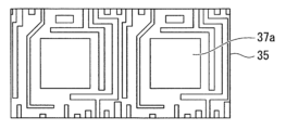
도 1은 본 기술의 제1 실시 형태에 관한 고체 촬상 장치의 일 구성예를 도시하는 칩 레이아웃도이다.
도 2는 본 기술의 제1 실시 형태에 관한 고체 촬상 장치의 일 구성예를 도시하는 블록도이다.
도 3은 본 기술의 제1 실시 형태에 관한 고체 촬상 장치의 화소의 일 구성예를 도시하는 등가 회로도이다.
도 4는 본 기술의 제1 실시 형태에 관한 고체 촬상 장치의 화소 어레이부 및 주변부의 개략 구성을 도시하는 모식적 종단면도이다.
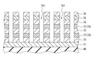
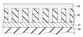
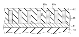
도 5는 도 4의 메타서피스 구조체의 부분을 확대한 주요부 확대 모식적 종단면도이다.
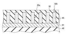
도 6은 도 5의 일부를 확대한 주요부 확대 모식적 종단면도이다.
도 7은 필러의 평면 레이아웃 패턴의 일례를 도시하는 도면이다.
도 8a는 반도체 웨이퍼의 평면 구성을 도시하는 도면이다.
도 8b는 도 8a의 A 영역을 확대해서 칩 형성 영역의 구성을 도시하는 도면이다.
도 9a는 본 기술의 제1 실시 형태에 관한 고체 촬상 장치의 제조 방법을 도시하는 모식적 공정 종단면도이다.
도 9b는 도 9a에 이은 모식적 공정 종단면도이다.
도 9c는 도 9b에 이은 모식적 공정 종단면도이다.
도 9d는 도 9c에 이은 모식적 공정 종단면도이다.
도 9e는 도 9d에 이은 모식적 공정 종단면도이다.
도 9f는 도 9e에 이은 모식적 공정 종단면도이다.
도 9g는 도 9f에 이은 모식적 공정 종단면도이다.
도 9h는 도 9g에 이은 모식적 공정 종단면도이다.
도 9i는 도 9h에 이은 모식적 공정 종단면도이다.
도 9j는 도 9i의 일부를 확대한 모식적 종단면도이다.
도 9k는 도 9j에 이은 모식적 공정 종단면도이다.
도 9l은 도 9k에 이은 모식적 공정 종단면도이다.
도 10은 제1 실시 형태의 변형예의 메타서피스 구조체의 일부를 도시하는 모식적 종단면도이다.
도 11은 필러의 평면 형상의 종류를 도시하는 도면이다.
도 12는 필러의 평면 레이아웃 패턴의 다른 예를 도시하는 도면이다.
도 13a는 본 기술의 제2 실시 형태에 관한 고체 촬상 장치의 제조 방법에 포함되는 메타서피스 구조체의 형성 공정을 도시하는 모식적 공정 종단면도이다.
도 13b는 도 13a에 이은 모식적 공정 종단면도이다.
도 13c는 도 13b에 이은 모식적 공정 종단면도이다.
도 13d는 도 13c에 이은 모식적 공정 종단면도이다.
도 13e는 도 13d에 이은 모식적 공정 종단면도이다.
도 13f는 도 13e에 이은 모식적 공정 종단면도이다.
도 14는 본 기술의 제3 실시 형태에 관한 고체 촬상 장치의 일 구성예를 도시하는 모식적 종단면도이다.
도 15는 본 기술의 제4 실시 형태에 관한 고체 촬상 장치의 일 구성예를 도시하는 모식적 종단면도이다.
도 16은 필러 직경과 위상 어긋남의 상관도이다.
도 17은 위상의 턴을 설명하기 위한 도면이다.
도 18은 본 기술의 제5 실시 형태에 관한 고체 촬상 장치의 화소 어레이부 및 주변부의 일 구성예를 도시하는 모식적 종단면도이다.
도 19는 도 18의 메타서피스 구조체의 부분을 확대한 주요부 모식적 종단면도이다.
도 20a는 본 기술의 제5 실시 형태에 관한 고체 촬상 장치의 제조 방법에 있어서, 메타서피스 구조체의 형성 공정을 도시하는 모식적 공정 종단면도이다.
도 20b는 도 20a에 이은 모식적 공정 종단면도이다.
도 20c는 도 20b에 이은 모식적 공정 종단면도이다.
도 20d는 도 20c에 이은 모식적 공정 종단면도이다.
도 20e는 도 20d에 이은 모식적 공정 종단면도이다.
도 20f는 도 20e에 이은 모식적 공정 종단면도이다.
도 20g는 도 20f에 이은 모식적 공정 종단면도이다.
도 20h는 도 20g에 이은 모식적 공정 종단면도이다.
도 21은 본 기술의 제6 실시 형태에 관한 고체 촬상 장치의 메타서피스 구조체의 일 구성예를 도시하는 주요부 모식적 종단면도이다.
도 22a는 본 기술의 제6 실시 형태에 관한 고체 촬상 장치의 제조 방법에 있어서, 메타서피스 구조체의 형성 공정을 도시하는 모식적 공정 종단면도이다.
도 22b는 도 22a에 이은 모식적 공정 종단면도이다.
도 22c는 도 22b에 이은 모식적 공정 종단면도이다.
도 23은 본 기술의 제7 실시 형태에 관한 고체 촬상 장치의 메타서피스 구조체의 일 구성예를 도시하는 주요부 모식적 종단면도이다.
도 24a는 본 기술의 제7 실시 형태에 관한 고체 촬상 장치의 제조 방법에 있어서, 메타서피스 구조체의 형성 공정을 도시하는 모식적 공정 종단면도이다.
도 24b는 도 24a에 이은 모식적 공정 종단면도이다.
도 24c는 도 24b에 이은 모식적 공정 종단면도이다.
도 24d는 도 24c에 이은 모식적 공정 종단면도이다.
도 24e는 도 24d에 이은 모식적 공정 종단면도이다.
도 24f는 도 24e에 이은 모식적 공정 종단면도이다.
도 24g는 도 24f에 이은 모식적 공정 종단면도이다.
도 24h는 도 24g에 이은 모식적 공정 종단면도이다.
도 25는 본 기술의 제8 실시 형태에 관한 고체 촬상 장치에 있어서, 메타서피스 구조체의 일 구성예를 도시하는 주요부 모식적 종단면도이다.
도 26a는 본 기술의 제8 실시 형태에 관한 고체 촬상 장치의 제조 방법에 있어서, 메타서피스 구조체의 형성 공정을 도시하는 모식적 공정 종단면도이다.
도 26b는 도 26a에 이은 모식적 공정 종단면도이다.
도 26c는 도 26b에 이은 모식적 공정 종단면도이다.
도 27a는 본 기술의 제9 실시 형태에 관한 고체 촬상 장치에 있어서, 메타서피스 구조체의 일 구성예를 도시하는 주요부 모식적 종단면도이다.
도 27b는 도 27a의 메타서피스 구조체의 주요부 모식적인 평면도이다.
도 28a는 본 기술의 제9 실시 형태에 관한 고체 촬상 장치의 제조 방법에 있어서, 메타서피스 구조체의 형성 공정을 도시하는 모식적 공정 종단면도이다.
도 28b는 도 28a에 이은 모식적 공정 종단면도이다.
도 28c는 도 28b에 이은 모식적 공정 종단면도이다.
도 29는 본 기술의 제9 실시 형태의 변형예 1에 관한 고체 촬상 장치에 있어서, 메타서피스 구조체의 일 구성예를 도시하는 주요부 모식적 종단면도이다.
도 30a는 본 기술의 제9 실시 형태의 변형예 2에 관한 고체 촬상 장치의 제조 방법에 있어서, 메타서피스 구조체의 형성 공정을 도시하는 모식적 공정 종단면도이다.
도 30b는 도 30a에 이은 모식적 공정 종단면도이다.
도 30c는 도 30b에 이은 모식적 공정 종단면도이다.
도 31a는 필러의 쓰러짐을 설명하기 위한 도면이다.
도 31b는 필러의 쓰러짐을 설명하기 위한 도면이다.
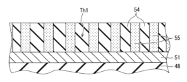
도 32는 본 기술의 제10 실시 형태에 관한 고체 촬상 장치의 화소 어레이부 및 주변부의 개략 구성을 도시하는 모식적 종단면도이다.
도 33은 도 32의 메타서피스 구조체의 부분을 확대한 주요부 모식적 종단면도이다.
도 34a는 본 기술의 제10 실시 형태에 관한 고체 촬상 장치의 제조 방법에 있어서, 메타서피스 구조체 형성 공정을 도시하는 모식적 공정 종단면도이다.
도 34b는 도 34a에 이은 모식적 공정 종단면도이다.
도 34c는 도 34b에 이은 모식적 공정 종단면도이다.
도 34d는 도 34c에 이은 모식적 공정 종단면도이다.
도 34e는 도 34d에 이은 모식적 공정 종단면도이다.
도 35a는 본 기술의 제11 실시 형태에 관한 고체 촬상 장치의 제조 방법에 있어서, 메타서피스 구조체의 형성 공정을 도시하는 모식적 공정 종단면도이다.
도 35b는 도 35a에 이은 모식적 공정 종단면도이다.
도 35c는 도 35b에 이은 모식적 공정 종단면도이다.
도 35d는 도 35c에 이은 모식적 공정 종단면도이다.
도 36a는 본 기술의 제12 실시 형태에 관한 고체 촬상 장치의 제조 방법에 있어서, 메타서피스 구조체의 형성 공정을 도시하는 모식적 공정 종단면도이다.
도 36b는 도 36a에 이은 모식적 공정 종단면도이다.
도 36c는 도 36b에 이은 모식적 공정 종단면도이다.
도 36d는 도 36c에 이은 모식적 공정 종단면도이다.
도 36e는 도 36d에 이은 모식적 공정 종단면도이다.
도 36f는 도 36e에 이은 모식적 공정 종단면도이다.
도 37a는 본 기술의 제13 실시 형태에 관한 고체 촬상 장치의 제조 방법에 있어서, 메타서피스 구조체의 형성 공정을 도시하는 모식적 공정 종단면도이다.
도 37b는 도 37a에 이은 모식적 공정 종단면도이다.
도 37c는 도 37b에 이은 모식적 공정 종단면도이다.
도 37d는 도 37c에 이은 모식적 공정 종단면도이다.
도 38a는 본 기술의 제14 실시 형태에 관한 고체 촬상 장치의 제조 방법에 있어서, 메타서피스 구조체의 형성 공정을 도시하는 모식적 공정 종단면도이다.
도 38b는 도 38a에 이은 모식적 공정 종단면도이다.
도 38c는 도 38b에 이은 모식적 공정 종단면도이다.
도 38d는 도 38c에 이은 종단면도이다.
도 39는 본 기술의 제15 실시 형태에 관한 고체 촬상 장치의 화소 어레이부 및 주변부의 개략 구성을 도시하는 모식적 종단면도이다.
도 40은 도 39의 메타서피스 구조체를 확대한 주요부 모식적 종단면도이다.
도 41은 본 기술의 제16 실시 형태에 관한 고체 촬상 장치의 화소 어레이부 및 주변부의 개략 구성을 도시하는 모식적 종단면도이다.
도 42는 본 기술의 제17 실시 형태에 관한 고체 촬상 장치의 화소 어레이부 및 주변부의 개략 구성을 도시하는 모식적 종단면도이다.
도 43은 도 42의 차광막의 일 구성예를 도시하는 평면도이다.
도 44는 차광막의 변형예를 도시하는 평면도(그 1)이다.
도 45는 차광막의 변형예를 도시하는 평면도(그 2)이다.
도 46은 차광막의 변형예를 도시하는 평면도(그 3)이다.
도 47은 도 42의 분리 영역의 일 구성예를 도시하는 종단면도이다.
도 48은 분리 영역의 변형예를 도시하는 종단면도(그 1)이다.
도 49는 분리 영역의 변형예를 도시하는 종단면도(그 2)이다.
도 50은 분리 영역의 변형예를 도시하는 종단면도(그 3)이다.
도 51은 분리 영역의 변형예를 도시하는 종단면도(그 4)이다.
도 52는 분리 영역의 변형예를 도시하는 종단면도(그 5)이다.
도 53은 본 기술의 제18 실시 형태에 관한 고체 촬상 장치의 화소 어레이부의 개략 구성을 도시하는 모식적 종단면도이다.
도 54a는 도 53의 a54-a54선을 따른 횡단면 구조를 도시하는 도면이다.
도 54b는 도 53의 b54-b54선을 따른 횡단면 구조를 도시하는 도면이다.
도 54c는 도 53의 c54-c54선을 따른 횡단면 구조를 도시하는 도면이다.
도 54d는 도 53의 d54-d54선을 따른 횡단면 구조를 도시하는 도면이다.
도 55는 반도체층의 광 입사면측의 계면에 마련한 회절·산란 소자를 도시하는 도면이다.
도 56은 반도체층의 광 입사면측의 계면에 마련한 광 분기부를 도시하는 도면(그 1)이다.
도 57은 반도체층의 광 입사면측의 계면에 마련한 광 분기부를 도시하는 도면(그 2)이다.
도 58은 반도체층의 광 입사면측의 계면에 마련한 광 분기부를 도시하는 도면(그 3)이다.
도 59는 본 기술의 제19 실시 형태에 관한 광 검출 장치에 있어서, 프리즘 기능의 편향부(메타서피스 구조체)와 온 칩 렌즈의 조합을 도시하는 주요부 모식적 종단면도이다.
도 60은 프리즘 기능과 렌즈 기능을 겸비한 편향부와 온 칩 렌즈의 조합을 도시하는 주요부 모식적 종단면도이다.
도 61은 프리즘 기능의 편향부(메타서피스 구조체)와 이너 렌즈의 조합을 도시하는 주요부 모식적 종단면도이다.
도 62는 프리즘 기능(메타서피스 구조체)과 렌즈 기능을 겸비한 편향부와 이너 렌즈의 조합을 도시하는 주요부 모식적 종단면도이다.
도 63은 본 기술의 제20 실시 형태에 관한 광 검출 장치에 있어서, 차광 벽의 구성을 도시하는 주요부 모식적 종단면도(그 1)이다.
도 64는 차광 벽의 구성을 도시하는 주요부 모식적 종단면도(그 2)이다.
도 65는 차광 벽의 구성을 도시하는 주요부 모식적 종단면도(그 3)이다.
도 66은 차광 벽의 구성을 도시하는 주요부 모식적 종단면도(그 4)이다.
도 67은 본 기술의 제21 실시 형태에 관한 광 검출 장치에 있어서, 광전 변환부의 분할의 구성을 도시하는 평면도(그 1)이다.
도 68은 광전 변환부의 분할의 구성을 도시하는 평면도(그 2)이다.
도 69는 본 기술의 제22 실시 형태에 관한 광 검출 장치에 있어서, 일반적인 안료, 혹은 염료를 포함하는 컬러 필터를 편향부 상에 구비한 구성예를 도시하는 주요부 모식적 종단면도이다.
도 70은 컬러 필터를 편향부 상에 구비한 구성예를 도시하는 주요부 모식적 종단면도이다.
도 71은 컬러 필터의 배열 예를 도시하는 평면도이다.
도 72는 플라스몬 필터와의 조합을 도시하는 주요부 모식적 종단면도이다.
도 73은 플라스몬 필터의 모식적인 평면도이다.
도 74는 GMR 필터와의 조합을 도시하는 주요부 모식적 종단면도이다.
도 75는 GMR 필터의 회절 격자와 클래드·코어 구조를 도시하는 모식적인 평면도이다.
도 76은 굴절률이 다른 적층 필터와의 조합을 도시하는 주요부 모식적 종단면도이다.
도 77은 굴절률이 다른 적층 필터의 일부를 확대한 도면이다.
도 78은 수직 입력에 필요한 위상차를 설명하기 위해서 도시하는 도면이다.
도 79는 어떤 방위의 프리즘 각에 대응하는 위상차 맵을 도시하는 도면이다.
도 80은 위상차와 필러 직경을 연관지은 위상차 library를 도시하는 특성도이다.
도 81은 각 필러의 위상차를 필러 직경으로 치환하는 처리를 설명하기 위해서 도시하는 도면이다.
도 82는 광 검출기의 화각을 도시하는 평면도이다.
도 83은 상고마다의 필러의 배치 예를 도시하는 평면도이다.
도 84는 렌즈 기능과 프리즘 기능을 겸비한 위상차 맵을 도시하는 도면이다.
도 85는 렌즈의 위상차 맵을 설명하기 위해서 도시하는 도면이다.
도 86은 본 기술의 제23 실시 형태에 관한 전자 기기의 개략 구성을 도시하는 도면이다.
도 87은 본 기술의 제24 실시 형태에 관한 전자 기기의 개략 구성을 도시하는 도면이다.1 is a chip layout diagram showing an example of a configuration of a solid-state imaging device according to the first embodiment of the present technology.
FIG. 2 is a block diagram showing a configuration example of a solid-state imaging device according to the first embodiment of the present technology.
FIG. 3 is an equivalent circuit diagram showing an example of a configuration of a pixel of a solid-state imaging device according to the first embodiment of the present technology.
FIG. 4 is a schematic longitudinal cross-sectional view showing the schematic configuration of the pixel array portion and peripheral portion of the solid-state imaging device according to the first embodiment of the present technology.
FIG. 5 is an enlarged schematic longitudinal cross-sectional view of a main part of the metasurface structure of FIG. 4.
Figure 6 is an enlarged schematic longitudinal cross-sectional view of a portion of Figure 5.
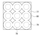
Figure 7 is a diagram showing an example of a planar layout pattern of a pillar.
FIG. 8A is a diagram showing the planar configuration of a semiconductor wafer.
FIG. 8B is an enlarged view of area A of FIG. 8A and shows the configuration of the chip formation area.
FIG. 9A is a schematic process longitudinal cross-sectional view showing a method of manufacturing a solid-state imaging device according to the first embodiment of the present technology.
Figure 9b is a schematic longitudinal cross-sectional view of the process following Figure 9a.
Figure 9c is a schematic longitudinal cross-sectional view of the process following Figure 9b.
Figure 9d is a schematic longitudinal cross-sectional view of the process following Figure 9c.
Figure 9e is a schematic longitudinal cross-sectional view of the process following Figure 9d.
Figure 9f is a schematic longitudinal cross-sectional view of the process following Figure 9e.
Figure 9g is a schematic longitudinal cross-sectional view of the process following Figure 9f.
Figure 9h is a schematic longitudinal cross-sectional view of the process following Figure 9g.
Figure 9i is a schematic longitudinal cross-sectional view of the process following Figure 9h.
FIG. 9J is a schematic longitudinal cross-sectional view enlarging part of FIG. 9I.
Figure 9k is a schematic longitudinal cross-sectional view of the process following Figure 9j.
Figure 9l is a schematic longitudinal cross-sectional view of the process following Figure 9k.
Fig. 10 is a schematic longitudinal cross-sectional view showing a part of the metasurface structure of a modification of the first embodiment.
Fig. 11 is a diagram showing types of planar shapes of fillers.
Figure 12 is a diagram showing another example of a planar layout pattern of a pillar.
FIG. 13A is a schematic longitudinal cross-sectional view showing the process of forming a metasurface structure included in the method for manufacturing a solid-state imaging device according to the second embodiment of the present technology.
FIG. 13B is a schematic longitudinal cross-sectional view of the process following FIG. 13A.
FIG. 13C is a schematic longitudinal cross-sectional view of the process following FIG. 13B.
FIG. 13D is a schematic longitudinal cross-sectional view of the process following FIG. 13C.
FIG. 13E is a schematic longitudinal cross-sectional view of the process following FIG. 13D.
Figure 13f is a schematic longitudinal cross-sectional view of the process following Figure 13e.
Fig. 14 is a schematic longitudinal cross-sectional view showing an example of the configuration of a solid-state imaging device according to the third embodiment of the present technology.
Fig. 15 is a schematic longitudinal cross-sectional view showing an example of the configuration of a solid-state imaging device according to the fourth embodiment of the present technology.
Figure 16 is a correlation diagram between pillar diameter and phase shift.
Figure 17 is a diagram for explaining phase turns.
Fig. 18 is a schematic longitudinal cross-sectional view showing an example of the configuration of the pixel array portion and peripheral portion of the solid-state imaging device according to the fifth embodiment of the present technology.
FIG. 19 is an enlarged schematic longitudinal cross-sectional view of a portion of the metasurface structure of FIG. 18.
FIG. 20A is a schematic longitudinal cross-sectional view showing the process of forming a metasurface structure in the method for manufacturing a solid-state imaging device according to the fifth embodiment of the present technology.
Figure 20b is a schematic longitudinal cross-sectional view of the process following Figure 20a.
Figure 20c is a schematic longitudinal cross-sectional view of the process following Figure 20b.
Figure 20d is a schematic longitudinal cross-sectional view of the process following Figure 20c.
FIG. 20E is a schematic longitudinal cross-sectional view of the process following FIG. 20D.
Figure 20f is a schematic longitudinal cross-sectional view of the process following Figure 20e.
Figure 20g is a schematic longitudinal cross-sectional view of the process following Figure 20f.
Figure 20h is a schematic longitudinal cross-sectional view of the process following Figure 20g.
Fig. 21 is a schematic longitudinal cross-sectional view of a main part showing an example of the configuration of the metasurface structure of the solid-state imaging device according to the sixth embodiment of the present technology.
FIG. 22A is a schematic longitudinal cross-sectional view showing the process of forming a metasurface structure in the method for manufacturing a solid-state imaging device according to the sixth embodiment of the present technology.
Figure 22b is a schematic longitudinal cross-sectional view of the process following Figure 22a.
Figure 22c is a schematic longitudinal cross-sectional view of the process following Figure 22b.
Fig. 23 is a schematic longitudinal cross-sectional view of the main part showing an example of the configuration of the metasurface structure of the solid-state imaging device according to the seventh embodiment of the present technology.
FIG. 24A is a schematic longitudinal cross-sectional view showing the process of forming a metasurface structure in the method for manufacturing a solid-state imaging device according to the seventh embodiment of the present technology.
Figure 24b is a schematic longitudinal cross-sectional view of the process following Figure 24a.
Figure 24c is a schematic longitudinal cross-sectional view of the process following Figure 24b.
Figure 24d is a schematic longitudinal cross-sectional view of the process following Figure 24c.
Figure 24e is a schematic longitudinal cross-sectional view of the process following Figure 24d.
Figure 24f is a schematic longitudinal cross-sectional view of the process following Figure 24e.
Figure 24g is a schematic longitudinal cross-sectional view of the process following Figure 24f.
Figure 24h is a schematic longitudinal cross-sectional view of the process following Figure 24g.
FIG. 25 is a schematic longitudinal cross-sectional view of a main part showing an example of a configuration of a metasurface structure in the solid-state imaging device according to the eighth embodiment of the present technology.
FIG. 26A is a schematic longitudinal cross-sectional view showing the process of forming a metasurface structure in the method for manufacturing a solid-state imaging device according to the eighth embodiment of the present technology.
Figure 26b is a schematic longitudinal cross-sectional view of the process following Figure 26a.
Figure 26c is a schematic longitudinal cross-sectional view of the process following Figure 26b.
FIG. 27A is a schematic longitudinal cross-sectional view of a main part showing an example of a configuration of a metasurface structure in the solid-state imaging device according to the ninth embodiment of the present technology.
FIG. 27B is a schematic plan view of the main part of the metasurface structure of FIG. 27A.
FIG. 28A is a schematic longitudinal cross-sectional view showing the process of forming a metasurface structure in the method for manufacturing a solid-state imaging device according to the ninth embodiment of the present technology.
Figure 28b is a schematic longitudinal cross-sectional view of the process following Figure 28a.
Figure 28c is a schematic longitudinal cross-sectional view of the process following Figure 28b.
FIG. 29 is a schematic longitudinal cross-sectional view of a main part showing an example of a configuration of a metasurface structure in a solid-state imaging device according to
FIG. 30A is a schematic longitudinal cross-sectional view showing the process of forming a metasurface structure in the method for manufacturing a solid-state imaging device according to
Figure 30b is a schematic longitudinal cross-sectional view of the process following Figure 30a.
FIG. 30C is a schematic longitudinal cross-sectional view of the process following FIG. 30B.
Figure 31a is a diagram for explaining the collapse of the pillar.
Figure 31b is a diagram for explaining the collapse of the pillar.
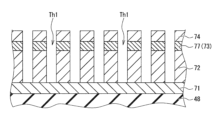
Fig. 32 is a schematic longitudinal cross-sectional view showing the schematic configuration of the pixel array portion and peripheral portion of the solid-state imaging device according to the tenth embodiment of the present technology.
FIG. 33 is an enlarged schematic longitudinal cross-sectional view of a portion of the metasurface structure of FIG. 32.
Fig. 34A is a schematic longitudinal cross-sectional view showing the metasurface structure forming process in the method for manufacturing a solid-state imaging device according to the tenth embodiment of the present technology.
Figure 34b is a schematic longitudinal cross-sectional view of the process following Figure 34a.
Figure 34c is a schematic longitudinal cross-sectional view of the process following Figure 34b.
Figure 34d is a schematic longitudinal cross-sectional view of the process following Figure 34c.
Figure 34e is a schematic longitudinal cross-sectional view of the process following Figure 34d.
FIG. 35A is a schematic longitudinal cross-sectional view showing the process of forming a metasurface structure in the method for manufacturing a solid-state imaging device according to the 11th embodiment of the present technology.
Figure 35b is a schematic longitudinal cross-sectional view of the process following Figure 35a.
Figure 35c is a schematic longitudinal cross-sectional view of the process following Figure 35b.
Figure 35d is a schematic longitudinal cross-sectional view of the process following Figure 35c.
Fig. 36A is a schematic longitudinal cross-sectional view showing the process of forming a metasurface structure in the method for manufacturing a solid-state imaging device according to the twelfth embodiment of the present technology.
Figure 36b is a schematic longitudinal cross-sectional view of the process following Figure 36a.
Figure 36c is a schematic longitudinal cross-sectional view of the process following Figure 36b.
Figure 36d is a schematic longitudinal cross-sectional view of the process following Figure 36c.
Figure 36e is a schematic longitudinal cross-sectional view of the process following Figure 36d.
Figure 36f is a schematic longitudinal cross-sectional view of the process following Figure 36e.
Fig. 37A is a schematic longitudinal cross-sectional view showing the process of forming a metasurface structure in the method for manufacturing a solid-state imaging device according to the 13th embodiment of the present technology.
Figure 37b is a schematic longitudinal cross-sectional view of the process following Figure 37a.
Figure 37c is a schematic longitudinal cross-sectional view of the process following Figure 37b.
Figure 37d is a schematic longitudinal cross-sectional view of the process following Figure 37c.
FIG. 38A is a schematic longitudinal cross-sectional view showing the process of forming a metasurface structure in the method for manufacturing a solid-state imaging device according to the fourteenth embodiment of the present technology.
Figure 38b is a schematic longitudinal cross-sectional view of the process following Figure 38a.
Figure 38c is a schematic longitudinal cross-sectional view of the process following Figure 38b.
Figure 38d is a longitudinal cross-sectional view following Figure 38c.
Fig. 39 is a schematic longitudinal cross-sectional view showing the schematic configuration of the pixel array portion and peripheral portion of the solid-state imaging device according to the 15th embodiment of the present technology.
Figure 40 is an enlarged schematic longitudinal cross-sectional view of the main part of the metasurface structure of Figure 39.
Fig. 41 is a schematic longitudinal cross-sectional view showing the schematic configuration of the pixel array portion and peripheral portion of the solid-state imaging device according to the 16th embodiment of the present technology.
Fig. 42 is a schematic longitudinal cross-sectional view showing the schematic configuration of the pixel array portion and peripheral portion of the solid-state imaging device according to the 17th embodiment of the present technology.
FIG. 43 is a plan view showing an example of the configuration of the light shielding film in FIG. 42.
Fig. 44 is a plan view (Part 1) showing a modified example of the light shielding film.
Fig. 45 is a plan view (Part 2) showing a modified example of the light shielding film.
Figure 46 is a plan view showing a modified example of the light shielding film (Part 3).
FIG. 47 is a vertical cross-sectional view showing an example of the configuration of the separation area in FIG. 42.
Fig. 48 is a vertical cross-sectional view (Part 1) showing a modified example of the separation region.
Fig. 49 is a vertical cross-sectional view (Part 2) showing a modified example of the separation area.
Fig. 50 is a vertical cross-sectional view (Part 3) showing a modified example of the separation region.
Fig. 51 is a vertical cross-sectional view (Part 4) showing a modified example of the separation region.
Fig. 52 is a vertical cross-sectional view (5) showing a modified example of the separation region.
Fig. 53 is a schematic longitudinal cross-sectional view showing the schematic configuration of the pixel array portion of the solid-state imaging device according to the 18th embodiment of the present technology.
FIG. 54A is a diagram showing a cross-sectional structure taken along line a54-a54 in FIG. 53.
FIG. 54B is a diagram showing a cross-sectional structure taken along line b54-b54 in FIG. 53.
FIG. 54C is a diagram showing a cross-sectional structure taken along line c54-c54 in FIG. 53.
FIG. 54D is a diagram showing a cross-sectional structure taken along line d54-d54 in FIG. 53.
Figure 55 is a diagram showing a diffraction/scattering element provided at the interface on the light incident surface side of the semiconductor layer.
Fig. 56 is a diagram (Part 1) showing an optical branching portion provided at the interface of the semiconductor layer on the light incident surface side.
Fig. 57 is a diagram (Part 2) showing an optical branching portion provided at the interface of the semiconductor layer on the light incident surface side.
Fig. 58 is a diagram (Part 3) showing an optical branching portion provided at the interface of the semiconductor layer on the light incident surface side.
Fig. 59 is a schematic longitudinal cross-sectional view of the main part showing the combination of a deflection portion (metasurface structure) with a prism function and an on-chip lens in the light detection device according to the 19th embodiment of the present technology.
Fig. 60 is a schematic longitudinal cross-sectional view of the main part showing the combination of a deflection unit with both a prism function and a lens function and an on-chip lens.
Figure 61 is a schematic longitudinal cross-sectional view of the main part showing the combination of a prism-functioning deflection portion (metasurface structure) and an inner lens.
Fig. 62 is a schematic longitudinal cross-sectional view of the main part showing the combination of a deflection part and an inner lens having both a prism function (metasurface structure) and a lens function.
Fig. 63 is a schematic longitudinal cross-sectional view (Part 1) of the main part showing the configuration of a light-shielding wall in the light detection device according to the twentieth embodiment of the present technology.
Figure 64 is a schematic longitudinal cross-sectional view (Part 2) of the main part showing the structure of the light-shielding wall.
Figure 65 is a schematic longitudinal cross-sectional view of the main part (part 3) showing the structure of the light-shielding wall.
Figure 66 is a schematic longitudinal cross-sectional view of the main part (Part 4) showing the structure of the light-shielding wall.
Figure 67 is a plan view (Part 1) showing the division structure of the photoelectric conversion section in the light detection device according to the 21st embodiment of the present technology.
Fig. 68 is a plan view (part 2) showing the configuration of the division of the photoelectric conversion section.
Fig. 69 is a schematic longitudinal cross-sectional view of the main part showing a configuration example in which a color filter containing a general pigment or dye is provided on the deflection portion of the light detection device according to the 22nd embodiment of the present technology.
Fig. 70 is a schematic longitudinal cross-sectional view of the main part showing a configuration example in which a color filter is provided on the deflection portion.
Fig. 71 is a plan view showing an example of the arrangement of color filters.
Figure 72 is a schematic longitudinal cross-sectional view of main parts showing combination with a plasmon filter.
Figure 73 is a schematic plan view of a plasmon filter.
Figure 74 is a schematic longitudinal cross-sectional view of main parts showing combination with a GMR filter.
Figure 75 is a schematic plan view showing the diffraction grating and clad core structure of the GMR filter.
Figure 76 is a schematic longitudinal cross-sectional view of main parts showing combination with laminated filters with different refractive indices.
Figure 77 is an enlarged view of a part of a stacked filter with different refractive index.
FIG. 78 is a diagram illustrating the phase difference required for vertical input.
Figure 79 is a diagram showing a phase difference map corresponding to a prism angle in a certain orientation.
Figure 80 is a characteristic diagram showing a phase difference library linking phase difference and pillar diameter.
FIG. 81 is a diagram illustrating the process of replacing the phase difference of each pillar with the pillar diameter.
Figure 82 is a plan view showing the angle of view of the photodetector.
Figure 83 is a plan view showing an example of the arrangement of pillars for each height.
Fig. 84 is a diagram showing a phase difference map combining a lens function and a prism function.
Figure 85 is a diagram shown to explain the phase difference map of the lens.
Figure 86 is a diagram showing the schematic configuration of an electronic device according to the 23rd embodiment of the present technology.
Figure 87 is a diagram showing the schematic configuration of an electronic device according to the 24th embodiment of the present technology.
이하, 도면을 참조하여 본 기술의 실시 형태를 상세하게 설명한다.Hereinafter, embodiments of the present technology will be described in detail with reference to the drawings.
또한, 이하의 설명에서 참조하는 도면의 기재에 있어서, 동일 또는 유사한 부분에는 동일 또는 유사한 부호를 붙이고 있다. 단, 도면은 모식적인 것이며, 두께와 평면 치수의 관계, 각 층의 두께의 비율 등은 현실의 것과는 다른 것에 유의해야 한다. 따라서, 구체적인 두께나 치수는 이하의 설명을 참작하여 판단해야 할 것이다.In addition, in the drawings referred to in the following description, identical or similar parts are given identical or similar symbols. However, it should be noted that the drawings are schematic, and the relationship between thickness and planar dimensions, the ratio of the thickness of each layer, etc. are different from those in reality. Therefore, specific thickness and dimensions should be determined by taking into account the following description.
또한, 도면 상호간에 있어서도 서로의 치수 관계나 비율이 다른 부분이 포함되어 있는 것은 물론이다. 또한, 본 명세서 중에 기재된 효과는 어디까지나 예시이며 한정되는 것은 아니고, 또 다른 효과가 있어도 된다.In addition, it goes without saying that parts with different dimensional relationships or ratios are included among the drawings. In addition, the effects described in this specification are only examples and are not limited, and other effects may occur.
또한, 본 명세서 중에서의 투명의 정의는, 광 검출 장치가 수광하는 상정의 파장 영역에 대해서, 그 부재의 투과율이 100%에 가까운 상태를 나타내는 것으로 한다. 예를 들어, 상정의 파장 영역에 대해서 재료 자체에 흡수가 있어도 극박(極薄)으로 가공되어 투과율이 100%에 가까운 부재라면 투명하다. 예를 들어, 근적외 영역에 사용되는 광 검출 장치의 경우에, 가시 영역에 있어서 흡수가 큰 부재이어도, 근적외 영역에서 투과율이 100%에 가까우면 투명이라고 할 수 있다. 혹은, 다소의 흡수 성분이나 반사 성분이 있었다고 해도, 그 영향이 광 검출 장치의 감도 사양과 대조해서 허용할 수 있는 범위라면, 투명으로 간주할 수 있는 것으로 본다.In addition, the definition of transparency in this specification is to indicate a state in which the transmittance of the member is close to 100% with respect to the assumed wavelength range in which the light detection device receives light. For example, even if there is absorption in the material itself in the assumed wavelength range, a member is transparent if it is processed to be ultrathin and has a transmittance close to 100%. For example, in the case of a light detection device used in the near-infrared region, even if the member has high absorption in the visible region, it can be said to be transparent if the transmittance is close to 100% in the near-infrared region. Alternatively, even if there is some absorption or reflection component, if the influence is within an allowable range compared to the sensitivity specifications of the light detection device, it can be considered transparent.
또한, 이하의 실시 형태는, 본 기술의 기술적 사상을 구체화하기 위한 장치나 방법을 예시하는 것이며, 구성을 하기의 것에 특정하는 것은 아니다. 즉, 본 기술의 기술적 사상은, 특허 청구 범위에 기재된 기술적 범위 내에서, 다양한 변경을 가할 수 있다.In addition, the following embodiments illustrate devices and methods for embodying the technical idea of the present technology, and do not specify the configuration as follows. In other words, the technical idea of the present technology can be subject to various changes within the technical scope described in the patent claims.
또한, 이하의 설명에서의 상하 등의 방향의 정의는, 단순히 설명의 편의상 정의이며, 본 기술의 기술적 사상을 한정하는 것은 아니다. 예를 들어, 대상을 90° 회전시켜 관찰하면 상하는 좌우로 변환되어 읽히고, 180° 회전시켜 관찰하면 상하는 반전되어 읽히는 것은 물론이다.In addition, the definitions of directions such as up and down in the following description are simply definitions for convenience of explanation and do not limit the technical idea of the present technology. For example, if you rotate an
또한, 이하의 실시 형태에서는, 공간 내에서 서로 직교하는 3방향에 있어서, 동일 평면 내에서 서로 직교하는 제1 방향 및 제2 방향을 각각 X 방향, Y 방향으로 하고, 제1 방향 및 제2 방향 각각과 직교하는 제3 방향을 Z 방향으로 한다. 그리고 이하의 실시 형태에서는, 후술하는 반도체층의 두께 방향을 Z 방향으로 해서 설명한다.In addition, in the following embodiment, in the three directions orthogonal to each other in space, the first and second directions orthogonal to each other in the same plane are referred to as the X direction and the Y direction, respectively, and the first and second directions The third direction orthogonal to each is referred to as the Z direction. In the following embodiments, the thickness direction of the semiconductor layer described later will be described as the Z direction.
〔제1 실시 형태〕[First Embodiment]
이 제1 실시 형태에서는, 광 검출 장치로서, 이면 조사형 CMOS(Complementary Metal Oxide Semiconductor) 이미지 센서인 고체 촬상 장치에 본 기술을 적용한 일례에 대해서 설명한다.In this first embodiment, an example of applying the present technology to a solid-state imaging device that is a back-illuminated CMOS (Complementary Metal Oxide Semiconductor) image sensor as a light detection device will be described.
≪고체 촬상 장치의 전체 구성≫≪Overall configuration of solid-state imaging device≫
먼저, 고체 촬상 장치(1A)의 전체 구성에 대해서 설명한다.First, the overall configuration of the solid-
도 1에 도시하는 바와 같이, 본 기술의 제1 실시 형태에 관한 고체 촬상 장치(1A)는, 평면으로 보았을 때의 이차원 평면 형상이 사각형인 반도체 칩(2)을 주체로 구성되어 있다. 즉, 고체 촬상 장치(1A)는, 반도체 칩(2)에 탑재되어 있다. 이 고체 촬상 장치(1A)(201)는, 도 86에 도시하는 바와 같이, 광학 렌즈(202)를 통해서 피사체로부터의 상광(입사광(206))을 도입하여, 촬상면 상에 결상된 입사광(206)의 광량을 화소 단위로 전기 신호로 변환해서 화소 신호로서 출력한다.As shown in FIG. 1, the solid-
도 1에 도시하는 바와 같이, 고체 촬상 장치(1A)가 탑재된 반도체 칩(2)은, 서로 직교하는 X 방향 및 Y 방향을 포함하는 이차원 평면에 있어서, 중앙부에 마련된 사각형의 화소 어레이부(2A)와, 이 화소 어레이부(2A)의 외측에 화소 어레이부(2A)를 둘러싸도록 해서 마련된 주변부(2B)를 구비하고 있다.As shown in FIG. 1, the
화소 어레이부(2A)는, 예를 들어 도 86에 도시하는 광학 렌즈(광학계)(202)에 의해 집광되는 광을 수광하는 수광면이다. 그리고 화소 어레이부(2A)에는, X 방향 및 Y 방향을 포함하는 이차원 평면에 있어서 복수의 화소(3)가 행렬상(어레이상)으로 배치되어 있다. 바꾸어 말하면, 화소(3)는, 이차원 평면 내에서 서로 직교하는 X 방향 및 Y 방향 각각의 방향으로 반복해서 배치되어 있다.The
도 1에 도시하는 바와 같이, 주변부(2B)에는, 복수의 본딩 패드(14)가 배치되어 있다. 복수의 본딩 패드(14) 각각은, 예를 들어 반도체 칩(2)의 이차원 평면에서의 4개의 변 각각의 변을 따라 배열되어 있다. 복수의 본딩 패드(14) 각각은, 반도체 칩(2)을 외부 장치와 전기적으로 접속할 때 사용되는 입출력 단자이다.As shown in FIG. 1, a plurality of
도 2에 도시하는 바와 같이, 반도체 칩(2)(고체 촬상 장치(1A))은, 화소 어레이부(2A)와, 수직 구동부(4)와, 칼럼 신호 처리부(5)와, 제어부(8)를 구비하고 있다. 화소 어레이부(2A)는, 화소(3)가 2차원 격자상으로 배치되어 구성된 것이다. 여기서, 화소(3)는, 조사된 광에 따른 화상 신호를 생성하는 것이다. 이 화소(3)는, 조사된 광에 따른 전하를 생성하는 광전 변환부(21)(도 3 참조)를 갖는다. 또한 화소(3)는, 도 3에 도시하는 화소 회로(29)를 더 갖는다. 이 화소 회로(29)는, 광전 변환부(21)에 의해 생성된 전하에 기초하는 화상 신호를 생성한다. 화상 신호의 생성은, 후술하는 수직 구동부(4)에 의해 생성된 제어 신호에 의해 제어된다.As shown in FIG. 2, the semiconductor chip 2 (solid-
도 2에 도시하는 바와 같이, 화소 어레이부(2A)에는, 신호선(11 및 12)이 XY 매트릭스상으로 배치되어 있다. 신호선(11)은, 화소(3)에서의 화소 회로(29)(도 3 참조)의 제어 신호를 전달하는 신호선이며, 화소 어레이부(2A)의 행마다 배치되고, 각 행에 배치되는 화소(3)에 대해서 공통으로 배선되어 있다. 신호선(12)은, 화소(3)의 화소 회로(29)에 의해 생성된 화상 신호를 전달하는 신호선이며, 화소 어레이부(2A)의 열마다 배치되고, 각 열에 배치되는 화소(3)에 대해서 공통으로 배선되어 있다. 이들 광전 변환부(21) 및 화소 회로(29)는, 반도체 칩(2)에 탑재되어 있다.As shown in FIG. 2,
수직 구동부(4)는, 화소(3)의 화소 회로(29)의 제어 신호를 생성하는 것이다. 이 수직 구동부(4)는, 생성한 제어 신호를, 신호선(11)을 통해서 화소(3)에 전달한다.The
칼럼 신호 처리부(5)는, 화소(3)에 의해 생성된 화상 신호를 처리하는 것이다. 이 칼럼 신호 처리부(5)는, 신호선(12)을 통해서 화소(3)로부터 전달된 화상 신호의 처리를 행한다. 칼럼 신호 처리부(5)에서의 처리에는, 예를 들어 화소(3)에서 생성된 아날로그의 화상 신호를 디지털의 화상 신호로 변환하는 아날로그/디지털 변환이 해당한다. 칼럼 신호 처리부(5)에 의해 처리된 화상 신호는, 고체 촬상 장치(1A)의 화상 신호로서 출력된다.The column
제어부(8)는, 고체 촬상 장치(1A) 전체를 제어하는 것이다. 이 제어부(8)는, 수직 구동부(4) 및 칼럼 신호 처리부(5)를 제어하는 제어 신호를 생성해서 출력함으로써, 고체 촬상 장치(1A)의 제어를 행한다. 제어부(8)에 의해 생성된 제어 신호는, 신호선(8a 및 8b)에 의해 수직 구동부(4) 및 칼럼 신호 처리부(5)에 대해서 각각 전달된다.The
또한, 수직 구동부(4), 칼럼 신호 처리부(5) 및 제어부(8)를 포함해서 로직 회로라고 칭하는 경우도 있다.In addition, it may be referred to as a logic circuit including the
도 3에 도시한 바와 같이, 화소(3)는, 광전 변환부(21)와, 화소 회로(29)를 구비하고 있다. 화소 회로(29)는, 전하 보유부(22)와, MOS 트랜지스터(23 내지 26)를 구비하고 있다.As shown in FIG. 3, the
광전 변환부(21)의 애노드는 접지되고, 캐소드는 MOS 트랜지스터(23)의 소스에 접속되어 있다. MOS 트랜지스터(23)의 드레인은, MOS 트랜지스터(24)의 소스, MOS 트랜지스터(25)의 게이트 전극 및 전하 보유부(22)의 일단부에 접속되어 있다. 전하 보유부(22)의 다른 일단부는 접지되어 있다.The anode of the
MOS 트랜지스터(25 및 26) 각각의 드레인은 전원선(Vdd)에 공통으로 접속되고, MOS 트랜지스터(25)의 소스는 MOS 트랜지스터(26)의 드레인에 접속되어 있다. MOS 트랜지스터(26)의 소스는, 출력 신호선(OUT)에 접속되어 있다. MOS 트랜지스터(23, 24 및 26)의 게이트 전극은, 각각 전송 신호선(TR), 리셋 신호선(RST) 및 선택 신호선(SEL)에 접속되어 있다.The drains of each of the
또한, 전송 신호선(TR), 리셋 신호선(RST) 및 선택 신호선(SEL)은, 신호선(11)을 구성한다. 또한, 출력 신호선(OUT)은, 신호선(12)을 구성한다. 광전 변환부(21)는, 상술한 바와 같이 조사된 광에 따른 전하를 생성하는 것이다. 이 광전 변환부(21)로서는, 예를 들어 포토다이오드를 사용할 수 있다. 또한, 전하 보유부(22) 및 MOS 트랜지스터(23 내지 26)는, 화소 회로(29)를 구성한다.Additionally, the transmission signal line (TR), reset signal line (RST), and selection signal line (SEL) constitute the
MOS 트랜지스터(23)는, 광전 변환부(21)의 광전 변환에 의해 생성된 전하를 전하 보유부(22)에 전송하는 트랜지스터이다. MOS 트랜지스터(23)에서의 전하의 전송은, 전송 신호선(TR)에 의해 전달되는 신호에 의해 제어된다.The
전하 보유부(22)는, MOS 트랜지스터(23)에 의해 전송된 전하를 보유하는 커패시터이다. MOS 트랜지스터(25)는, 전하 보유부(22)에 보유된 전하에 기초하는 신호를 생성하는 트랜지스터이다. MOS 트랜지스터(26)는, MOS 트랜지스터(25)에 의해 생성된 신호를 화상 신호로서 출력 신호선(OUT)에 출력하는 트랜지스터이다. 이 MOS 트랜지스터(26)는, 선택 신호선(SEL)에 의해 전달되는 신호에 의해 제어된다.The
MOS 트랜지스터(24)는, 전하 보유부(22)에 보유된 전하를 전원선(Vdd)에 배출함으로써 전하 보유부(22)를 리셋하는 트랜지스터이다. 이 MOS 트랜지스터(24)에 의한 리셋은, 리셋 신호선(RST)에 의해 전달되는 신호에 의해 제어되고, MOS 트랜지스터(23)에 의한 전하의 전송 전에 실행된다.The
또한, 이 리셋 시, MOS 트랜지스터(23)를 도통시킴으로써, 광전 변환부(21)의 리셋도 행할 수 있다. 이와 같이, 화소 회로(29)는, 광전 변환부(21)에 의해 생성된 전하를 화상 신호로 변환한다.Additionally, at the time of this reset, the
또한, MOS 트랜지스터(23 내지 26) 각각은, 게이트 절연막, 게이트 전극, 소스 영역 및 드레인 영역으로서 기능하는 한 쌍의 주 전극 영역을 포함하고, 게이트 절연막이 산화실리콘막으로 구성된 전계 효과 트랜지스터이다. MOS 트랜지스터 대신에, MIS 트랜지스터를 사용해도 된다.Additionally, each of the
≪고체 촬상 장치의 구체적인 구성≫≪Specific configuration of solid-state imaging device≫
이어서, 고체 촬상 장치(1A)의 구체적인 구성에 대해서 설명한다.Next, the specific configuration of the solid-
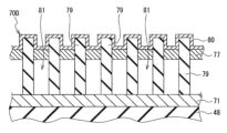
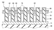
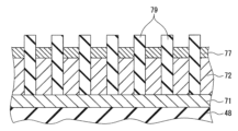
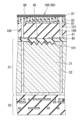
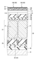
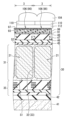
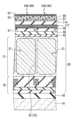
도 4에 도시하는 바와 같이, 반도체 칩(2)은, 반도체 기체(30)와, 이 반도체 기체(30)의 광 입사면측과는 반대측에 마련된 지지 기판(41)을 구비하고 있다.As shown in FIG. 4 , the
<반도체 기체><Semiconductor substrate>
반도체 기체(30)는, 복수의 광전 변환부(21)가 마련된 반도체층(31)과, 이 반도체층(31)의 두께 방향에 있어서 서로 반대측에 위치하는 제1면 S1 및 제2면 S2 중 제1면 S1측에 마련된 다층 배선층(35)을 구비하고 있다.The
또한, 반도체 기체(30)는, 반도체층(31)의 제2면 S2측에, 이 제2면 S2측으로부터 순차 적층된 고정 전하막(45), 절연막(46), 차광막(47) 및 절연막(48)을 더 구비하고 있다.In addition, the
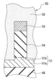
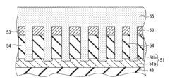
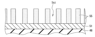
또한, 반도체 기체(30)는, 반도체층(31)의 제2면 S2측이며, 반도체층(31)의 제2면 S2측에 대해서, 반도체층(31)측과는 반대측에 마련된 메타서피스 구조체(50)를 더 구비하고 있다.In addition, the
여기서, 반도체층(31)의 제1면 S1을 소자 형성면 또는 주면, 제2면 S2를 광 입사면 또는 이면이라고 칭하는 경우도 있다. 이 제1 실시 형태의 고체 촬상 장치(1A)는, 반도체층(31)의 제2면(광 입사면, 이면) S2측으로부터 입사한 광을, 반도체층(31)에 마련된 광전 변환부(21)에서 광전 변환한다.Here, the first surface S1 of the
또한, 평면으로 보아란, 반도체층(31)의 두께 방향(Z 방향)를 따르는 방향으로 본 경우를 가리킨다.In addition, planar view refers to the case when viewed in a direction along the thickness direction (Z direction) of the
<반도체층><Semiconductor layer>
도 4에 도시하는 바와 같이, 반도체층(31)에는, 제1 도전형, 이 제1 실시 형태에서는 p형의 반도체 영역(33)과, 제2 도전형, 이 제1 실시 형태에서는 n형의 반도체 영역(34)이 마련되어 있다. 반도체층(31)으로서는, 예를 들어 Si 기판, SiGe 기판, InGaAs 기판 등을 사용할 수 있다. 이 제1 실시 형태에서는, 예를 들어 Si 기판을 사용하고 있다. 반도체층(31)은, 화소 어레이부(2A) 및 주변부(2B)에 걸쳐서 마련되어 있다.As shown in FIG. 4, the
도 4에 도시하는 바와 같이, p형의 반도체 영역(33)은, 반도체층(31)의 두께 방향(Z 방향)의 전역에 걸쳐서, 바꾸어 말하면 반도체층(31)의 제2면 S2 및 제1면 S1에 걸쳐서 마련되어 있다. 그리고 p형의 반도체 영역(33)은, 평면으로 보아 화소 어레이부(2A)의 전역에 마련되고, 또한 화소 어레이부(2A) 및 주변부(2B)에 걸쳐서 마련되어 있다.As shown in FIG. 4, the p-
n형의 반도체 영역(34)은, 화소(3)마다 p형의 반도체 영역(33) 중에 마련되고, 또한 반도체층(31)의 제2면 S2측 및 제1면 S1측에 걸쳐서 마련되어 있다. 즉, n형의 반도체 영역(34)은, 반도체층(31)의 제2면 S2측의 상면부, 반도체층(31)의 제1면 S1측의 하면부 및 측면부가 p형의 반도체 영역(33)으로 둘러싸여 있다.The n-
여기서, 상술한 광전 변환부(21)는, 주로 n형의 반도체 영역(34)으로 구성되고, p형의 반도체 영역(33)과 n형의 반도체 영역(34)에 의한 pn 접합형의 포토다이오드로서 구성되어 있다.Here, the
n형의 반도체 영역(34)(광전 변환부(21))의 상면부측 및 하면부측에 위치하는 p형의 반도체 영역(33), 바꾸어 말하면 반도체층(31)의 표리 양면에 면하는 p형의 반도체 영역(33)은, 암전류 억제를 위한 정공 전하 축적 영역을 겸하고 있다.A p-
n형의 반도체 영역(34)의 측면부에 위치하는 p형의 반도체 영역(33)은, 서로 인접하는 n형의 반도체 영역(34)을 전기적으로 분리하는 분리 영역(32)으로서 기능한다. 즉, 이 제1 실시 형태의 분리 영역(32)은 p형의 반도체 영역(33)으로 구성되어 있다. 그리고 n형의 반도체 영역(34)을 포함하는 광전 변환부(21)는, 분리 영역(32)으로 구획되어, 서로 인접하는 광전 변환부(21)와 전기적으로 분리되어 있다. 분리 영역(32)에는, 기준 전위로서 예를 들어 0V의 그라운드 전위가 인가된다.The p-
여기서, 도 4에는 도시하고 있지 않지만, 상술한 화소 회로(29)에 포함되는 MOS 트랜지스터(23 내지 26)는, 반도체층(31)의 제1면 S1측에 구성되어 있다. 이 제1 실시 형태에서는, MOS 트랜지스터(23 내지 26)는, 화소(3)마다 마련되어 있지만, 복수 화소에서 공유해서 구비할 수도 있다.Here, although not shown in FIG. 4, the
<다층 배선층><Multilayer wiring layer>
도 4에 도시하는 바와 같이, 다층 배선층(35)은, 반도체층(31)의 광 입사면(제2면 S2)측과는 반대측의 제1면 S1측에 마련되어 있고, 배선(37)을 포함하는 배선층이 층간 절연막(36)을 개재해서 복수단 적층된 구성으로 되어 있다.As shown in FIG. 4, the
다층 배선층(35)은, 화소(3)에 의해 생성된 화상 신호를 전달하는 것이다. 또한, 다층 배선층(35)은, 화소 회로(29)에 인가되는 신호의 전달을 또한 행한다. 구체적으로는, 다층 배선층(35)은, 도 3에서 설명한 신호선(출력 신호선(OUT), 전송 신호선(TR), 리셋 신호선(RST) 및 선택 신호선(SEL)) 및 전원선(Vdd)을 구성한다. 다층 배선층(35)과 화소 회로(29)의 사이는, 비아 플러그에 의해 접속되어 있다. 또한, 다층 배선층(35)의 배선층간도 비아 플러그에 의해 접속되어 있다. 다층 배선층(35)은, 예를 들어 알루미늄(Al)이나 구리(Cu) 등의 금속에 의해 구성할 수 있다. 비아 플러그는, 예를 들어 텅스텐(W)이나 Cu 등의 금속에 의해 구성할 수 있다. 다층 배선층(35)의 층간 절연막(36)에는, 예를 들어 산화실리콘막 등을 사용할 수 있다.The
이 다층 배선층(35)의 배선(37)을 통해서 각 화소(3)의 화소 트랜지스터가 구동된다. 다층 배선층(35)은, 반도체층(31)의 광 입사면측(제2면 S2측)과는 반대측에 배치되어 있으므로, 배선(37)의 배치 자유도가 향상된다. 다층 배선층(35)은, 화소 어레이부(2A) 및 주변부(2B)에 걸쳐서 마련되어 있다.The pixel transistor of each
<고정 전하막><Fixed charge film>
도 4에 도시하는 바와 같이, 고정 전하막(45)은, 화소 어레이부(2A) 및 주변부(2B)에 걸쳐서 마련되어 있다. 고정 전하막(45)은, 산소의 다이폴에 의한 부의 고정 전하를 갖고, 피닝을 강화하는 역할을 한다. 고정 전하막(45)은, 예를 들어 Hf, Al, 지르코늄, Ta 및 Ti 중 적어도 하나를 포함하는 산화물 또는 질화물에 의해 구성할 수 있다. 또한, 란탄, 세륨, 네오디뮴, 프로메튬, 사마륨, 유로퓸, 가돌리늄, 테르븀, 디스프로슘, 홀뮴, 툴륨, 이테르븀, 루테튬 및 이트륨 중 적어도 하나를 포함하는 산화물 또는 질화물에 의해 구성할 수도 있다. 또한, 고정 전하막(45)은, 산질화하프늄 또는 산질화알루미늄에 의해 구성할 수도 있다. 또한, 고정 전하막(45)에는, 절연성이 손상되지 않는 양의 실리콘이나 질소를 첨가할 수도 있다. 이에 의해, 내열성 등을 향상시킬 수 있다. 고정 전하막(45)은, 막 두께를 제어하거나, 혹은 다층 적층함으로써, 굴절률이 높은 Si 기판에 대한 반사 방지막의 역할을 겸비하는 것이 바람직하다.As shown in FIG. 4, the fixed
<절연막><Insulating film>
도 4에 도시하는 바와 같이, 절연막(46)은, 반도체층(31)의 제2면 S2에 인접해서 마련되어, 반도체층(31)을 절연하는 막이다. 이 절연막(46)은, 예를 들어 SiO2에 의해 구성되며, 반도체층(31)의 이면측(제2면 S2측)을 절연함과 함께 보호한다. 절연막(46)은, 화소 어레이부(2A) 전역에 마련되고, 나아가 화소 어레이부(2A) 및 주변부(2B)에 걸쳐서 마련되어 있어도 된다.As shown in FIG. 4, the insulating
<차광막><Light shield>
도 4에 도시하는 바와 같이, 차광막(47)은, 메타서피스 구조체(50)보다 반도체층(31)측에 배치되어 있음과 함께 평면으로 보아 화소(3)의 경계와 중첩하는 영역에 배치되어, 인접한 화소(3)로부터 새어 들어가는 미광을 차폐한다. 이 차광막(47)은, 광을 차광하는 재료이면 된다. 예를 들어, 차광성이 강하고, 또한 미세 가공, 예를 들어 에칭으로 고정밀도로 가공할 수 있는 재료로서, Al, W, 혹은 구리 등의 금속막으로 형성하는 것이 바람직하다. 그 밖에도 은, 금, 백금, Mo, Cr, Ti, 니켈, 철 및 텔루륨 등이나 이들 금속을 포함하는 합금에 의해 구성할 수 있다. 또한, 이들 재료를 복수 적층해서 구성할 수도 있다. 하지의 절연막(46)과의 밀착성을 높이기 위해서, 차광막(47) 아래에 배리어 메탈, 예를 들어 Ti, Ta, W, Co, Mo, 혹은 그들의 합금, 혹은 그들의 질화물, 혹은 그들의 산화물, 혹은 그들의 탄화물을 구비해도 된다. 또한, 이 차광막(47)으로, 광학적 흑색 레벨을 결정하는 화소의 차광을 겸해도 되며, 주변 회로 영역에 대한 노이즈 방지를 위한 차광을 겸해도 된다. 차광막(47)은, 가공 중의 축적 전하에 의한 플라스마 대미지로 파괴되지 않도록 접지되어 있는 것이 바람직하다. 접지 구조는 화소 배열 내에 형성해도 되지만, 도체 모두가 전기적으로 연결되도록 한 상태에서 도 4에 도시하는 유효 영역의 외측 영역에 접지 구조를 구비해도 된다. 즉, 도 4에 도시하는 바와 같이, 주변부(2B)의 차광막(47)을 반도체층(31)의 p형의 반도체 영역(33)과 전기적으로 접속하는 구성으로 해도 된다. 차광막(47)은, 반도체층(31)의 광 입사면측(제2면 S2측)과 메타서피스 구조체(50)의 사이에 위치하고, 화소(3) 내의 적어도 일부에 개구를 갖는다.As shown in FIG. 4, the
<절연막><Insulating film>
도 4에 도시하는 바와 같이, 절연막(48)은, 절연막(46) 및 차광막(47)에 인접해서 배치된 막이다. 이 절연막(48)은, 반도체층(31)의 제2면 S2측(이면측, 광 입사면측)을 절연함과 함께 평탄화한다. 이 절연막(46)은, 예를 들어 광투과성이 우수한 산화실리콘막으로 구성되어 있다. 절연막(48)은, 화소 어레이부(2A) 전역에 마련되고, 나아가 화소 어레이부(2A) 및 주변부(2B)에 걸쳐서 마련되어 있어도 된다.As shown in FIG. 4 , the insulating
<지지 기판><Support substrate>
도 4에 도시하는 바와 같이, 지지 기판(41)은, 화소 어레이부(2A) 및 주변부(2B)에 걸쳐서 마련되어 있다. 지지 기판(41)은, 고체 촬상 장치(1A)의 제조 공정에서 반도체층(31) 등을 보강하고, 지지하는 기판이며, 예를 들어 실리콘 기판 등으로 구성되어 있다. 지지 기판(41)은, 플라스마 접합, 혹은 접착 재료로 반도체 기체(30)와 맞붙여서, 반도체층(31) 등을 지지한다. 지지 기판(41)은, 로직 회로를 구비하고 있어도 되고, 기판간에 접속 비아를 형성함으로써, 다양한 주변 회로 기능을 수직 쌓기함으로써 칩 사이즈를 축소하는 것이 가능해진다.As shown in FIG. 4, the
<휨 교정막><Bending correction film>
도 4에 도시하는 바와 같이, 다층 배선층(35)의 반도체층(31)측과는 반대측에는, 반도체 기체(30)와 지지 기판(41)을 접합할 때의 웨이퍼의 휨을 경감하기 위한 휨 교정막(42)이 마련되어 있다. 이 휨 교정막(42)은, 웨이퍼 전체를 덮고 있다.As shown in FIG. 4, on the side of the
<메타서피스 구조체><Metasurface structure>
도 4에 도시하는 바와 같이, 메타서피스 구조체(50)는, 반도체층(31)의 광 입사면측(제2면 S2측)에서 화소(3)마다 마련되어, 입사광을 광전 변환부(21)에 유도한다. 즉, 화소(3)는, 반도체층(31)에 마련된 광전 변환부(21)와, 반도체층(31)의 광 입사면측에 배치되며, 또한 입사광을 광전 변환부(21)에 유도하는 메타서피스 구조체(50)를 구비하고 있다. 그리고 광전 변환부(21)는, 메타서피스 구조체(50)에 의해 유도된 입사광을 광전 변환한다.As shown in FIG. 4 , the
도 4 및 도 5에 도시한 바와 같이, 이 제1 실시 형태의 메타서피스 구조체(50)는, 반도체층(31)의 제2면 S2측에 대해서, 반도체층(31)측과는 반대측의 광 입사면측에 마련되어 있다. 이 제1 실시 형태의 메타서피스 구조체(50)는, 절연막(48)의 광 입사면측에, 취급하는 입사광의 파장보다 짧은 거리로 서로 배치되는 복수의 필러(54)와, 서로 인접하는 필러(54)의 사이에 충전된 투명재(55)를 포함한다. 또한, 이 제1 실시 형태의 메타서피스 구조체(50)는, 필러(54)의 반도체층(31)측에 마련된 반사 방지막(51)과, 필러(54)의 반도체층(31)측과는 반대측에 마련된 반사 방지막(53)과, 투명재(55)의 반도체층(31)측과는 반대측에 마련된 투명 보호막(57)을 더 포함하고 있어도 된다.As shown in FIGS. 4 and 5, the
메타서피스 구조체(50)는, 화소 어레이부(2A)에 한정하는 것은 아니고, 주변부(2B)에 구비할 수도 있다. 주변부(2B)의 메타서피스 구조체(50)는, 모듈 렌즈로부터의 입사광, 혹은 세트 하우징으로부터의 미광 등이 주변부(2B)에서 반사해서 플레어나 고스트로 되어 화질 열화를 일으키지 않도록, 반사 방지하는 것이 목적으로 된다. 즉, 화소 특성을 높이기 위한 화소 어레이부(2A)와 설계 지침이 달라, 레이아웃을 구분 제작하는 것이 바람직하다. 예를 들어, 주변부(2B)의 메타서피스 구조체(50) 아래에 카본 블랙 등의 흡수체를 구비할 경우, 경사 입사로 흡수체 내에서의 광로 길이를 길게 해서 흡수 효율을 높이도록 메타서피스 구조체(50)를 설계해도 된다. 혹은, 세트 하우징 등의 전체를 고려하여, 주변부(2B)로부터의 반사광이 화소 어레이부(2A)에 재돌입하지 않는 각도가 되도록 메타서피스 구조체(50)를 구비해도 된다.The
<반사 방지막><Anti-reflective film>
도 4 및 도 5에 도시한 바와 같이, 반사 방지막(51)은, 화소 어레이부(2A) 전역에 마련되고, 나아가 주변부(2B)에 걸쳐서 마련되어 있어도 된다. 반사 방지막(51)은, 필러(54)의 보텀부(반도체층(31)측)의 굴절률 계면에 의한 광의 반사를 억제하기 위해서, 광 검출에서 상정되는 파장을 λ, 반사 방지막의 굴절률을 n이라 했을 때, 소위, λ/(4n) 규칙을 고려한 막 두께로 구성되어 있다. 나아가, 반사 방지 효과를 높이기 위해서, 굴절률이 다른 막을 적층시켜도 된다. 또한, 이 반사 방지막(51)은, 필러 형성막을 건식 에칭으로 가공해서 필러(54)를 형성할 때의 에칭 스토퍼층으로서 기능시켜도 된다. 반사 방지막(51)은, 필러(54)에 대해서 에칭 선택비를 취할 수 있는 재료로 구성되어 있다.As shown in FIGS. 4 and 5 , the
<필러><Filler>
도 4 및 도 5에 도시한 바와 같이, 복수의 필러(54) 각각의 필러(54)는, 주상으로 가공되어, 반사 방지막(51)의 상면측으로부터 상방을 향해서 연신되어 있다. 그리고 복수의 필러(54)는, 굵기, 혹은 배열 피치, 혹은 형상이 다른 필러(54)를 포함한다. 도 7에 복수의 필러(54)의 평면 레이아웃 패턴(복수의 필러(54)를 포함하는 필러군)의 일례를 나타낸다. 이러한 복수의 필러(54)의 평면 레이아웃 패턴(필러군)을 포함함으로써 국소적으로 광의 위상차가 바뀌어, 필러(54)의 레이아웃(배치 패턴)에 따라서 광의 배향을 제어하는 것이 가능해진다.As shown in FIGS. 4 and 5 , each of the plurality of
또한, 필러(54)의 평면 레이아웃 패턴은, 화소(3)마다 설정해도 되고, 또한, 복수의 화소(3)에서 1개의 평면 레이아웃 패턴을 공유해도 된다. 또한, 필러(54)의 평면 레이아웃 패턴은, 전체 화소(3)에서 공통으로 해도 되고, 또한, 소정의 화소(3)에서 다른 평면 레이아웃 패턴을 혼재시켜도 된다. 도 12에, 복수의 필러(54)의 평면 레이아웃 패턴의 다른 일례를 나타낸다.Additionally, the planar layout pattern of the
<반사 방지막><Anti-reflective film>
도 4 및 도 5에 도시한 바와 같이, 반사 방지막(53)은, 필러(54)의 반도체층(31)측과는 반대측의 일단부에 마련되어 있다. 반사 방지막(53)은, 필러(54)의 상부의 굴절률 계면에 의한 광(입사광)의 반사를 억제하기 위해서, 소위, λ/(4n) 규칙을 고려한 막 두께로 구성되어 있다. 나아가, 반사 방지 효과를 높이기 위해서, 굴절률이 다른 막을 적층시켜도 된다. 필러(54)를 가공하기 전에 반사 방지막(53)을 성막함으로써, 굴절률이 높은 필러(54)의 부분에만 구비하도록 해도 된다.As shown in FIGS. 4 and 5 , the
<투명재><Transparent material>
도 4 및 도 5에 도시한 바와 같이, 투명재(55)는, 필러와 필러의 사이를 접속해서 지지하는 투명 지지체로서, 서로 인접하는 필러(54)와 필러(54)의 사이를 충전하고, 나아가 복수의 필러(54) 및 반사 방지막(53) 각각을 덮고 있어도 된다. 투명재(55)는, 예를 들어 화소 어레이부(2A) 전역에 마련되고, 나아가 화소 어레이부(2A) 및 주변부(2B)에 걸쳐서 마련되어 있어도 된다. 이 투명재(55)에 의해, 필러(54)의 도괴나 조립에 있어서의 보호 테이프의 접착제 잔여물에 의한 불량을 억제할 수 있다. 투명재(55)와 필러(54)는 굴절률이 다르다.As shown in Figures 4 and 5, the
투명재(55)의 반사 방지막(51)으로부터의 두께 치수는, 필러(54)의 반사 방지막(51)으로부터의 높이에 반사 방지막(53)의 두께를 가산한 치수와 동일하거나, 혹은 더 크다.The thickness of the
<투명 보호막><Transparent shield>
도 4에 도시하는 바와 같이, 투명 보호막(57)은, 화소 어레이부(2A) 전역에 마련되고, 나아가 화소 어레이부(2A) 및 주변부(2B)에 걸쳐서 마련되어 있어도 된다. 투명 보호막(57)은, 무기 재료로 구성되어 있다. 이 제1 실시 형태에서는, 투명 보호막(57)은, 예를 들어 산화실리콘막으로 구성되어 있다.As shown in FIG. 4, the transparent
<필러의 재료><Material of filler>
필러(54)의 재료로서, 주로 NIR(근적외광) 용도의 경우는, 아몰퍼스 실리콘(a-Si), 폴리실리콘, 게르마늄(Ge)의 어느 재료를 사용하는 것이 바람직하다.As a material for the
또한, 주로 가시 영역 용도의 경우는, 산화티타늄, 산화니오븀, 산화탄탈, 산화알루미늄, 산화하프늄, 질화실리콘, 산화실리콘, 질화산화실리콘, 탄화실리콘, 산화탄화규소, 질화탄화실리콘, 산화지르코늄의 어느 재료, 혹은 이들 산화티타늄, 산화니오븀, 산화탄탈, 산화알루미늄, 산화하프늄, 질화실리콘, 산화실리콘, 질화산화실리콘, 탄화실리콘, 산화탄화규소, 질화탄화실리콘, 산화지르코늄의 적어도 2 이상 적층한 적층 구조체를 사용하는 것이 바람직하다.Additionally, in the case of mainly visible range applications, any of titanium oxide, niobium oxide, tantalum oxide, aluminum oxide, hafnium oxide, silicon nitride, silicon oxide, silicon nitride oxide, silicon carbide, silicon oxide carbide, silicon nitride carbide, and zirconium oxide. A laminated structure in which at least two of these materials or titanium oxide, niobium oxide, tantalum oxide, aluminum oxide, hafnium oxide, silicon nitride, silicon oxide, silicon nitride oxide, silicon carbide, silicon oxide carbide, silicon nitride carbide, and zirconium oxide are laminated. It is desirable to use .
<필러의 평면 형상><Plane shape of filler>
메타서피스 구조체(50)의 필러(54)의 평면 형상은, 실효 굴절률의 제어에 더하여, 편광 성분의 이방성 제어, 면적률에 의존한 반사 성분, 프로세스 가공성, 패턴 도괴 내성의 관점에서 결정된다. 도 11에 필러의 평면 형상의 베리에이션을 나타낸다.The planar shape of the
도 11에서, 편광 제어의 등방성이 우수한 것은 (1) 내지 (3)이다. 혹은 편광 시점에서, 수평과 수직, 혹은 45도와 135도의 방향의 축에 대해서 4회 대칭성이나 미러 반전 대상성을 갖는 것은 (4) 내지 (8)이다. 혹은, 편광 시점에서 일축성의 특성을 발휘하는 것은 (9) 내지 (21)이다. 나아가, (12)의 짧은 변을 가늘게 해서 제어할 때 패턴 도괴가 발생하는 경우, (22), (23)과 같은 쓰러짐 방지의 보조 패턴을 배치하는 것이 바람직하다. 동일한 단면적으로 비교했을 때, (3), (5), (11), (13), (17), (19)는 패턴 도괴 리스크를 회피해서 작은 실효 굴절률 차를 생기게 할 수 있다. 나아가, 동일 피치로 비교했을 때, 정방 배열에 대해서 (4), (5)가, 허니콤 구조에서는 (1) 내지 (3)이, 필러 충전율을 높이고, 위상차를 부여할 경우에 유리해진다.In Fig. 11, (1) to (3) have excellent polarization control isotropy. Or, at the point of polarization, it is (4) to (8) that has four-fold symmetry or mirror inversion with respect to the horizontal and vertical, or 45 and 135 degree axes. Alternatively, it is (9) to (21) that exhibits uniaxial characteristics at the point of polarization. Furthermore, if pattern collapse occurs when the short side of (12) is thinned and controlled, it is desirable to arrange auxiliary patterns to prevent collapse, such as (22) and (23). When compared with the same cross-sectional area, (3), (5), (11), (13), (17), and (19) can avoid the risk of pattern collapse and produce a small difference in effective refractive index. Furthermore, when compared at the same pitch, (4) and (5) are advantageous for the square arrangement, and (1) to (3) for the honeycomb structure are advantageous when increasing the filler filling rate and providing a phase difference.
<필러의 높이><Height of pillar>
필러(54)의 높이는, 파장, 필러와 투명재의 굴절률, 필러 형상이나 높이 등으로 규정되는 위상차 라이브러리에 대해서, 프로세스로 가공할 수 있는 필러 직경의 범위에서, 후술하는 2π 이상 위상을 회전시킬 수 있는 높이로 하는 것이 바람직하다.The height of the
도 16에 아몰퍼스 Si의 피치 350nm에서의 원형 필러의 위상차 라이브러리의 예를 나타낸다. 프로세스 가공 한계가 필러 직경 250nm인 경우, 필러 높이를 800nm로 설정하는 것이 적합하다.Figure 16 shows an example of a phase difference library of circular pillars of amorphous Si with a pitch of 350 nm. If the process machining limit is a pillar diameter of 250 nm, it is appropriate to set the pillar height to 800 nm.
<반사 방지막의 굴절률과 두께><Refractive index and thickness of anti-reflective film>
필러(54)의 상부, 혹은 필러(54)의 하부, 혹은 양쪽에, 반사파의 위상이 서로 상쇄되는 막 두께로, 굴절률이 다른 반사 방지막(51, 53)을 구비하는 것이 바람직하다. 구체적으로는, 반사 방지막(51, 53)의 두께는 대략 λ/(4n)로 하는 것이 바람직하다. 실제로는 다층막의 간섭 효과, 사입사 특성을 고려할 필요가 있어, 광학 시뮬레이션, 혹은 실측으로 최적화하는 것이 바람직하다.It is desirable to provide
<위상의 턴 방법><How to turn the phase>
도 17에 도시하는 바와 같이, 위상의 턴부는 산란이 발생해서 미광을 생기게 해 버린다. 나아가, 화소(3)마다 면적률이 다르면 반사 성분(감도 손실)이 바뀌어 버린다. 따라서, 하기 룰 (a), (b)로 위상을 턴시키는 것이 바람직하다.As shown in Fig. 17, scattering occurs at the turn portion of the phase, resulting in stray light. Furthermore, if the area ratio is different for each
(a) 화소 단위로 턴(a) Turn by pixel
(b) 화소 내 턴은 화소 중심 근방(b) The turn within the pixel is near the pixel center.
룰 (a)는 근방에 위치하는 화소의 면적률을 균일하게 하여, 반사율 변동을 억제하는 것이 가능해진다. 룰 (b)는, 턴부로부터의 미광이 화소 경계를 넘으면 크로스토크가 되어 특성이 열화되어 버리기 때문에, 턴과 각 화소 경계의 거리를 유지하는 것이 바람직하다. 즉, 대칭성의 점에서 화소 내 턴은, 화소 중심 근방을 통과하도록 설정하는 것이 적합하다.Rule (a) makes it possible to equalize the area ratio of pixels located nearby and suppress fluctuations in reflectance. Rule (b) is that if stray light from the turn crosses the pixel boundary, crosstalk occurs and the characteristics deteriorate, so it is desirable to maintain the distance between the turn and each pixel boundary. That is, in terms of symmetry, it is appropriate to set the turn within the pixel to pass near the center of the pixel.
<반사 방지막의 형상><Shape of anti-reflective film>
도 6에 도시하는 바와 같이, 반사 방지막(51)은, 필러(54)의 바로 아래 및 주위에 걸쳐서 2차원상으로 펼쳐지는 주요부(51a)와, 필러(54)의 바로 아래에서 주요부(51a)로부터 돌출되고, 또한 필러(54)의 보텀 폭보다 폭이 좁은 돌기부(51b)를 포함한다. 그리고 필러(54) 및 반사 방지막(51)의 돌기부(51b)는, 투명재(55)로 둘러싸여 있다. 즉, 반사 방지막(51)의 돌기부(51b)의 외측에서 필러(54)의 반사 방지막(51)측의 단부면(하면)과 반사 방지막(51)의 주요부(51a)의 사이에도 투명재(55)가 충전되어 있다. 이와 같이, 필러(54) 및 반사 방지막(51)의 돌기부(51b)가 투명재(55)로 둘러싸여 있음으로써, 앵커 효과에 의해 투명재(55)의 박리를 억제할 수 있다. 나아가, 필러의 보텀 폭보다 가늘게 가공되는 돌기부(51b)는 강성이 약해지기 때문에, 둥그스름한 형상으로 해서 응력 집중을 완화시키는 것이 바람직하다.As shown in FIG. 6, the
<실효 굴절률><Effective refractive index>
도 5에 도시한 바와 같이, 필러(54)의 일단부측 상면에서의 면적률을 고려한 실효 굴절률을 n1이라 하고, 필러(54)의 타단부측 하면 바로 아래에서의 반사 방지막(51)의 면적률을 고려한 실효 굴절률을 n2라 하고, 반사 방지막(51)의 굴절률을 n3이라 했을 때, 실효 굴절률은, n1>n2, n3>n2가 되도록 구비하는 것이, 굴절률의 불연속 계면의 영향이 적어, 반사 억제의 시점에서 바람직하다. 또한, 각 계면으로부터의 반사파의 위상이 서로 상쇄되도록 n2의 높이와 n3의 높이를 설정하는 것이 바람직하다.As shown in FIG. 5, the effective refractive index considering the area ratio on the upper surface of one end of the
<투명재의 재료><Material of transparent material>
필러(54)와 투명재(55)의 굴절률 차는 광의 위상차를 부여하기 위해서 0.3 이상인 것이 바람직하다. 투명재(55)는, 유기 재료 혹은 무기 재료로 구성되어 있다. 유기 재료로서는, 예를 들어 실록산계 수지, 스티렌계 수지, 아크릴계 수지, 스티렌-아크릴 공중합계 수지의 어느 것, 혹은 실록산계 수지, 스티렌계 수지, 아크릴계 수지, 스티렌-아크릴 공중합계 수지의 어느 것에 불소를 함유하는 재료, 혹은, 실록산계 수지, 스티렌계 수지, 아크릴계 수지, 스티렌-아크릴 공중합계 수지에 이들 수지보다 굴절률이 낮은 비즈를 내충전하는 재료를 사용할 수 있다.The difference in refractive index between the
무기 재료로서는, 산화실리콘, 산화니오븀, 산화탄탈, 산화알루미늄, 산화하프늄, 질화실리콘, 질화산화실리콘, 탄화실리콘, 산화탄화규소, 질화탄화실리콘, 산화지르코늄의 적어도 어느 재료를 사용할 수 있다. 또한, 이들 산화실리콘, 산화니오븀, 산화탄탈, 산화알루미늄, 산화하프늄, 질화실리콘, 질화산화실리콘, 탄화실리콘, 산화탄화규소, 질화탄화실리콘, 산화지르코늄의 어느 재료를 적어도 2 이상 적층한 적층 구조체로 구성할 수 있다.As the inorganic material, at least any of silicon oxide, niobium oxide, tantalum oxide, aluminum oxide, hafnium oxide, silicon nitride, silicon nitride oxide, silicon carbide, silicon oxide carbide, silicon nitride carbide, and zirconium oxide can be used. In addition, it is a laminate structure in which at least two of any of these materials, such as silicon oxide, niobium oxide, tantalum oxide, aluminum oxide, hafnium oxide, silicon nitride, silicon nitride oxide, silicon carbide, silicon oxide carbide, silicon nitride carbide, and zirconium oxide, are laminated. It can be configured.
또한, 여기서 개시한 고체 촬상 장치(1A)는, 이면 조사형을 나타내고 있지만, 이것에 한정하는 것은 아니고, 표면 조사형의 고체 촬상 장치, 나아가 유기 광전 변환막을 사용한 고체 촬상 장치 등에 적용할 수 있다.In addition, although the solid-
≪고체 촬상 장치의 제조 방법≫≪Method for manufacturing solid-state imaging device≫
이어서, 이 제1 실시 형태에 관한 고체 촬상 장치(1A)의 제조 방법에 대해서, 도 8a 및 도 8b, 그리고 도 9a 내지 도 9l을 사용하여 설명한다.Next, the manufacturing method of the solid-
도 8a는, 반도체 웨이퍼의 평면 구성을 도시하는 도면이며, 도 8b는, 도 8a의 A 영역을 확대해서 칩 형성 영역의 구성을 도시하는 도면이다.FIG. 8A is a diagram showing the planar configuration of a semiconductor wafer, and FIG. 8B is a diagram showing the configuration of a chip formation area by enlarging area A of FIG. 8A.
또한, 도 9a 내지 도 9l은, 고체 촬상 장치(1A)의 제조 방법을 도시하는 모식적 종단면도이다.9A to 9L are schematic longitudinal cross-sectional views showing the manufacturing method of the solid-
여기서, 도 8a 및 도 8b에 도시하는 바와 같이, 고체 촬상 장치(1A)는, 반도체 웨이퍼(60)의 칩 형성 영역(62)에 제작된다. 칩 형성 영역(62)은, 스크라이브 라인(61)으로 구획되어, 행렬상으로 복수 배치되어 있다. 도 8b에서는, X 방향 및 Y 방향 각각의 방향으로 3개씩 배치(3×3)된 9개의 칩 형성 영역(62)을 나타내고 있다. 그리고 이 복수의 칩 형성 영역(62)을 스크라이브 라인(61)을 따라 개개로 개편화함으로써, 고체 촬상 장치(1A)를 탑재한 반도체 칩(2)이 형성된다. 칩 형성 영역(62)의 개편화는, 이하에 설명하는 제조 공정을 실시해서 각 칩 형성 영역(62)에 고체 촬상 장치(1A)를 형성한 후에 행해진다.Here, as shown in FIGS. 8A and 8B, the solid-
또한, 스크라이브 라인(61)은 물리적으로 형성되어 있는 것은 아니다.Additionally, the
먼저, 도 9a에 도시하는 바와 같이, 반도체층(31)에, 분리 영역(32)으로 구획된 복수의 광전 변환부(21)를 형성한다. 분리 영역(32) 및 광전 변환부(21)는, 반도체층(31)에 p형의 반도체 영역(33)을 형성함과 함께, 이 p형의 반도체 영역(33) 중에 서로 이격되어 인접하는 복수의 n형의 반도체 영역(34)을 형성함으로써 구축할 수 있다. n형의 반도체 영역(34)(광전 변환부(21))의 상면부측 및 하면부측에 위치하는 p형의 반도체 영역(33)은, 암전류 억제를 위한 정공 전하 축적 영역을 겸한다. n형의 반도체 영역(34)의 측면부에 위치하는 p형의 반도체 영역(33)은, 서로 인접하는 n형의 반도체 영역(34)을 전기적으로 분리하는 분리 영역(32)으로서 기능한다.First, as shown in FIG. 9A, a plurality of
여기서, 이 제1 실시 형태에 관한 고체 촬상 장치(1A)의 제조 프로세스에서는, 이 공정 후에, 반도체층(31)의 제2면 S2측을 연삭해서 반도체층(31)의 두께를 얇게 하는 연삭 공정을 포함하고 있다. 따라서, p형의 반도체 영역(33)은, 반도체층(31)의 연삭 공정 후의 두께 이상의 깊이로 형성한다.Here, in the manufacturing process of the solid-
이어서, 상세하게 도시하고 있지 않지만, 반도체층(31)의 제1면 S1에 화소 회로(29)에 포함되는 MOS 트랜지스터(22 내지 26)를 형성함과 함께, 로직 회로에 포함되는 MOS 트랜지스터를 형성한다.Next, although not shown in detail,
이어서, 도 9b에 도시하는 바와 같이, 반도체층(31)의 제1면 S1측에 다층 배선층(35)을 형성한다. 다층 배선층(35)은, 배선(37)을 포함하는 배선층이 층간 절연막(36)을 개재해서 복수단 적층된 구성으로 되어 있다.Next, as shown in FIG. 9B, a
이 공정에 의해, 반도체층(31) 및 다층 배선층(35)을 포함하는 반도체 기체(30)가 형성된다.Through this process, the
이어서, 도 9c에 도시하는 바와 같이, 휨 교정막(42)을 개재해서 반도체 기체(30)의 다층 배선층(35)측과 지지 기판(41)의 주면측을 접합한다. 이 접합은, 플라스마 접합에 의해 행한다. 이 접합은, 접착재에 의해 행해도 된다. 휨 교정막(42)은, 지지 기판(41)의 접합면측에 미리 마련되어 있다.Next, as shown in FIG. 9C, the
이 공정에 의해, 반도체 기체(30) 및 지지 기판(41)을 포함하는 반도체 웨이퍼(60)가 형성된다.Through this process, a
이어서, 도 9d에 도시하는 바와 같이, 반도체층(31)의 두께를 얇게 한다. 구체적으로는, 반도체층(31)의 제2면 S2측을 습식 에칭이나 건식 에칭에 의해 에칭해서 반도체층(31)의 두께를 얇게 한 후, 또한 반도체층(31)의 제2면 S2측을 CMP법으로 연삭해서 반도체층(31)을 소정의 두께까지 얇게 한다. 반도체층(31)의 두께는 취급하는 파장 영역에 따라서 설정한다. 예를 들어, 이것에 한정되지 않지만, 가시광 영역만이라면 2 내지 6㎛의 범위가 바람직하고, 근적외선 영역도 검지하는 것이면 3 내지 15㎛의 범위로 하는 것이 바람직하다.Next, as shown in FIG. 9D, the thickness of the
이어서, 도 9e에 도시하는 바와 같이, 반도체층(31)의 제2면 S2측에, 고정 전하막(45), 절연막(46), 차광막(47) 및 절연막(48)을 이 순으로 형성한다.Next, as shown in FIG. 9E, a fixed
고정 전하막(45)은, CVD(Chemical Vapor Deposition)법, 스퍼터링법, 혹은 원자층 증착(ALD: Atomic Layer Deposition)법에 의해 형성할 수 있다. ALD법을 채용한 경우에는, 원자층 레벨로 양호한 커버리지가 얻어져서, 고정 전하막(45)의 성막 중에 계면 준위를 저감시키는 산화실리콘막을 동시에 형성하는 것이 가능하게 되어, 적합하다. 고정 전하막(45)은, 막 두께를 제어하거나, 혹은 다층 적층함으로써, 굴절률이 높은 Si 반도체층에 대한 반사 방지막의 역할을 겸비하는 것이 바람직하다.The fixed
절연막(46)을 예를 들어 ALD법으로 성막한 산화실리콘막으로 구성하는 경우, 얇게 하면 블리스터 현상에 의한 막 박리가 발생하기 쉬워지기 때문에, 절연막(46)은, 적어도 20nm 이상, 바람직하게는 50nm 이상의 두께로 하는 것이 좋다.When the insulating
차광막(47)은, 상술한 재료를 CVD법, 혹은 스퍼터링법 등을 사용하여 성막한다. 또한, 금속을 전기적으로 들뜬 상태에서 가공하면 플라스마 대미지가 발생할 가능성이 있기 때문에, 화소 어레이부(2A)의 외측 영역에서, 예를 들어 수㎛ 폭의 레지스트의 에칭 패턴을 전사하고, 이방성 에칭이나 습식 에칭으로 홈부를 형성해서 반도체층(31)의 제2면 S2를 노출시킨 상태에서, 차광 재료를 반도체층(31)에 접지시켜 성막하는 것이 바람직하다. 차광 재료가 접지되는 반도체층(31)의 영역은, 예를 들어 p형의 반도체 영역(33)을 그라운드 전위로 해 두는 것이 바람직하다. 차광 재료는 복수 적층해서 구성하여, 예를 들어 티타늄, 질화티타늄, 혹은 그들의 적층막을 절연막(46)에 대한 밀착층으로 해도 된다. 혹은, 티타늄, 질화티타늄, 혹은 그들의 적층막만을 차광막(47)으로서 사용할 수도 있다. 또한, 차광 재료는, 화상 신호의 흑색 레벨을 산출하기 위한 화소인 흑색 레벨 산출 화소(도시하지 않음)의 차광막, 혹은, 주변 회로의 오동작을 방지하는 위한 차광막을 겸할 수도 있다.The light-shielding
차광막(47)은, 차광 재료에 대해서, 예를 들어 광전 변환부에 광을 유도하기 위한 개구부와, 나아가, 패드부, 스크라이브 라인부 등에 레지스트의 에칭 패턴을 형성하고, 이방성 에칭 등에 의해 차광 재료를 부분적으로 제거함으로써 형성할 수 있다. 필요에 따라 약액 세정으로 잔사를 제거한다.The light-shielding
절연막(48)은, 절연막(46) 상에 차광막을 덮도록 하여, 예를 들어 산화실리콘막을 CVD법이나, 스퍼터링법 등을 사용해서 성막함으로써 형성된다. 절연막(48)은, 성막한 후, CMP로 평탄화된다.The insulating
이어서, 도 9f에 도시하는 바와 같이, 절연막(48)의 반도체층(31)측과는 반대측(절연막(48)의 광 입사면측)에, 반사 방지막(51), 필러 형성막(52), 반사 방지막(53)을 이 순으로 형성한다. 구체적으로는, 반사 방지막(51)은, 예를 들어 125nm 정도의 막 두께의 질화실리콘(Si3N4)막을 CVD법으로 성막함으로써 형성한다. 필러 형성막(52)은, 예를 들어 800nm 정도의 막 두께의 아몰퍼스 실리콘을 CVD법으로 성막함으로써 형성한다. 반사 방지막(53)은, 예를 들어 125nm 정도의 막 두께의 질화실리콘을 CVD법으로 성막함으로써 형성한다. 필러 형성막(52)으로서는, 아몰퍼스 실리콘 외에, 상술한 재료를 사용할 수 있다.Next, as shown in FIG. 9F, on the side opposite to the
이어서, 도 9g에 도시하는 바와 같이, 반사 방지막(53)의 반도체층(31)측과는 반대측(절연막(48)의 광 입사면측)에, 소정의 평면 레이아웃 패턴의 레지스트 마스크 RM1을 형성한다. 이 레지스트 마스크 RM1은, 주지의 포토리소그래피 기술로 형성한다. 레지스트 마스크 RM1의 평면 레이아웃 패턴은, 필러(54)의 평면 레이아웃 패턴을 규정한다.Next, as shown in FIG. 9G, a resist mask RM1 with a predetermined plan layout pattern is formed on the side of the
이어서, 레지스트 마스크 RM1을 에칭 마스크로서 사용해서, 레지스트 마스크 RM1의 외측의 반사 방지막(53) 및 필러 형성막(52)을 순차 에칭하여, 도 9h에 도시하는 바와 같이, 주상의 필러(54) 및 반사 방지막(53)을 형성한다. 복수의 필러(54)는, 화소(3)마다 소정의 평면 레이아웃 패턴을 구성한다. 반사 방지막(53)은, 필러(54)의 반도체층(31)측과는 반대측의 일단부에 필러(54)마다 형성된다.Next, using the resist mask RM1 as an etching mask, the
이 공정에서, 반사 방지막(53) 및 필러 형성막(52)의 에칭은, 예를 들어 이방성 건식 에칭을 사용하여 행한다. 그리고 필러 형성막(52)의 에칭은, 반사 방지막(53 및 51)에 대해서 선택성을 갖는 에칭 조건에서 행한다.In this process, the
레지스트 마스크 RM1의 선택비가 불충분할 경우에는, 레지스트 패턴을 하드마스크, 예를 들어 산화실리콘막에 한번 전사하여, 하드마스크 너머로 에칭하는 하드마스크 프로세스로 가공해도 된다.If the selectivity of the resist mask RM1 is insufficient, the resist pattern may be transferred once to a hard mask, for example, a silicon oxide film, and processed through a hard mask process in which the pattern is etched beyond the hard mask.
또한, 필러(54)의 하부에 있는 반사 방지막(51)은, 광학적인 반사 방지를 목적으로 구비하지만, 그 기능에 더하여, 에칭 시의 에칭 스토퍼층으로 해도 된다. 혹은, 반사 방지막(51)은, 반사 방지 설계하지 않고, 에칭 스토퍼층으로서만 구비해도 된다. 반사가 증가해서 감도가 저하되지만, 성막의 공정수를 삭감하는 것이 가능해진다.Additionally, the
이어서, 습식 약액 세정을 행하여, 도 9i에 도시하는 바와 같이, 레지스트 마스크 RM1을 제거함과 함께, 가공 잔사를 제거한다. 약액 세정 후, 통상의 원심 탈수 건조에서는, 약액 건조 시에 표면 장력의 불균형으로 패턴 도괴의 리스크가 높아져 버린다. 그 대책으로서, 표면 장력이 약한 IPA로 치환하고 나서 건조시켜도 되고, 나아가, 초임계 세정을 사용해도 된다.Next, wet chemical cleaning is performed to remove the resist mask RM1 and processing residues, as shown in FIG. 9I. In normal centrifugal dehydration drying after chemical cleaning, the risk of pattern collapse increases due to imbalance in surface tension during chemical drying. As a countermeasure, it may be replaced with IPA, which has a weak surface tension, and then dried, or furthermore, supercritical washing may be used.
이 공정에서, 반사 방지막(51)이 등방적으로 에칭되어, 도 9j에 도시하는 바와 같이, 필러(54)의 바로 아래 및 주위에 걸쳐서 2차원상으로 펼쳐지는 주요부(51a)와, 필러(54)의 바로 아래에서 주요부(51a)로부터 돌출되고, 또한 필러(54)의 보텀 폭보다 폭이 좁고 둥그스름한 돌기부(51b)를 포함하는 반사 방지막(51)이 형성된다. 둥그스름한 밑단 확대 형상에 의해 응력 집중이 완화되어, 반사 방지막(51)의 돌기부(51b)를 기점으로 하는 패턴 도괴를 억제할 수 있다.In this process, the
이어서, 도 9k에 도시하는 바와 같이, 서로 인접하는 필러(54)의 사이에 투명재(55)를 형성한다. 투명재(55)는 투명하고, 필러(54)와의 굴절률 차가 큰 재료를 사용한다. 투명재(55)는, 예를 들어 불소 함유 실록산계 수지를, 회전 도포법으로 형성한다. 투명재(55)로서는, 상술한 유기 재료 및 무기 재료를 사용할 수 있다. 투명재(55)는, 필러(54)의 높이보다 두꺼운 막 두께로 형성한다.Next, as shown in FIG. 9K, a
이 공정에서, 필러(54)는 투명재(55)로 지지되므로, 조립 시의 보호 테이프를 박리할 때의 필러 파손이나, 필러의 간극에 들어간 접착제 잔여물의 불량을 회피하고, 시장에서의 낙하 충격에 의한 고장 모드를 회피하는 것이 가능해진다.In this process, the
또한, 이 공정에서, 반사 방지막(51)의 돌기부(51b)의 외측에서 필러(54)의 반사 방지막(51)측의 단부면(하면)과 반사 방지막(51)의 주요부(51a)의 사이에도 투명재(55)가 충전되어, 필러(54) 및 반사 방지막(51)의 돌기부(51b)가 투명재(55)로 둘러싸이기 때문에, 앵커 효과에 의해 투명재(55)의 박리를 억제할 수 있다.Additionally, in this step, between the end surface (lower surface) of the
이어서, 도 9l에 도시하는 바와 같이, 투명재(55)의 반도체층측과는 반대측(투명재(55)의 광 입사면측)에 무기 재료로서 예를 들어 산화실리콘막을 포함하는 투명 보호막(57)을 CVD법에 의해 형성한다.Next, as shown in FIG. 9L, a transparent
이 공정에 의해, 제1 실시 형태의 메타서피스 구조체(50)가 거의 완성된다.Through this process, the
이 후, 도 1에 도시하는 본딩 패드(14)를 노출시키는 본딩 개구부를 형성함으로써, 도 4에 도시하는 고체 촬상 장치(1A)가 거의 완성된다. 이 본딩 개구부의 형성은 레지스트 마스크를 사용하여 행하는데, 이 레지스트 마스크의 제거 시에 투명재(55)는 무기 재료의 투명 보호막(57)으로 덮여 있기 때문에, 이 레지스트 마스크의 제거에 의한 투명재(55)의 대미지를 회피하는 것이 가능해진다.After this, the solid-
또한, 이 공정에 의해, 도 8a 및 도 8b에 도시하는 반도체 웨이퍼(60)가 거의 완성된다. 반도체 웨이퍼(60)의 복수의 칩 형성 영역(62) 각각에 고체 촬상 장치(1A)가 형성된다.Additionally, through this process, the
이 후, 반도체 웨이퍼(60)의 복수의 칩 형성 영역(62)을 스크라이브 라인(61)을 따라 개개로 개편화함으로써, 고체 촬상 장치(1A)를 탑재한 반도체 칩(2)이 형성된다.Thereafter, the plurality of
≪제1 실시 형태의 주된 효과≫≪Main effect of the first embodiment≫
이어서, 이 제1 실시 형태의 주된 효과에 대해서 설명한다.Next, the main effects of this first embodiment will be described.
이 제1 실시 형태에 관한 고체 촬상 장치(1A)는, 메타서피스 구조체(50)를 구비하고 있다. 그리고 메타서피스 구조체(50)는, 서로 인접하는 필러(54)와 필러(54)의 사이에 충전된 투명재(55)를 구비하고 있다. 이 때문에, 필러(54)는 투명재(55)에 지지되므로, 필러(54)의 도괴를 억제하는 것이 가능해진다.The solid-
또한, 메타서피스 구조체(50)는, 반사 방지막(51)을 구비하고 있다. 그리고 반사 방지막(51)은, 필러(54)의 바로 아래 및 주위에 걸쳐서 2차원상으로 펼쳐지는 주요부(51a)와, 필러(54)의 바로 아래에서 주요부(51a)로부터 돌출되고, 또한 필러(54)의 보텀 폭보다 폭이 좁고 둥그스름한 돌기부(51b)를 포함한다. 그리고 필러(54) 및 반사 방지막(51)의 돌기부(51b)는, 투명재(55)로 둘러싸여 있다. 이 때문에, 앵커 효과에 의해 투명재(55)의 박리를 억제하는 것이 가능해진다. 나아가, 둥그스름한 밑단 확대의 형상에 의해 응력 집중이 완화되어, 반사 방지막(51)의 돌기부(51b)를 기점으로 하는 패턴 도괴를 억제할 수 있다.Additionally, the
이 제1 실시 형태에 관한 고체 촬상 장치(1A)는, 서로 인접하는 필러(54)와 필러(54)의 사이에 투명재(55)를 충전하는 충전 공정을 구비하고 있다. 이 때문에, 필러(54)가 투명재(55)로 지지된 메타서피스 구조체(50)를 갖는 고체 촬상 장치(1A)를 제공하는 것이 가능해진다.The solid-
≪제1 실시 형태의 변형예≫≪Modification of the first embodiment≫
상술한 제1 실시 형태에서는, 필러(54)의 하지층으로서의 반사 방지막(51)이 주요부(51a) 및 돌기부(51b)를 포함하는 구성으로 되어 있는 경우에 대해서 설명하였다. 이에 반해, 이 변형예에서는, 도 10에 도시하는 바와 같이, 필러(54)의 하지층으로서의 반사 방지막(51)이, 평면으로 보아 서로 인접하는 필러(54)의 사이의 부분에 오목부(51c)를 갖는 구성으로 되어 있다.In the above-described first embodiment, the case where the
이 경우, 필러(54)의 일단부측 상면에서의 굴절률을 n1이라 하고, 필러(54)의 타단부측 하면에서의 굴절률을 n2라 하고, 반사 방지막(51)의 오목부(51c)의 저면에서의 굴절률을 n3이라 했을 때, 실효 굴절률은, n1>n2, n3>n2를 충족함으로써, 계단식으로 고굴절되는 구성으로 할 수 있어, 오목부(51c)가 없는 형상에 비하여, 굴절률의 불연속 계면의 영향이 완화되어, 반사 억제의 시점에서 바람직하다. 이러한 형상은 보텀부의 가공에서 에칭이 앞으로 갈 수록 가늘어지도록 가스종을 제어해서 형성해도 되고, 혹은, 미리 반사 방지막(51)에 대해서, 리소그래피 공정과 이방성 에칭으로 오목부(51c)를 형성해도 된다.In this case, let the refractive index at the upper surface of the one end side of the
〔제2 실시 형태〕[Second Embodiment]
본 기술의 제2 실시 형태에 관한 고체 촬상 장치의 제조 방법에 대해서, 도 13a 내지 도 13j를 사용하여 설명한다.The manufacturing method of the solid-state imaging device according to the second embodiment of the present technology will be described using FIGS. 13A to 13J.
먼저, 제1 실시 형태의 도 9a 내지 도 9e에 도시하는 공정과 마찬가지의 공정을 실시한 후, 도 13a에 도시하는 바와 같이, 절연막(48)의 반도체층(31)측과는 반대측(절연막(48)의 광 입사면측)에, 반사 방지막(51) 및 투명재(55)를 이 순으로 형성한다. 반사 방지막(51)은, 예를 들어 125nm 정도의 막 두께의 질화실리콘막을 CVD법으로 성막함으로써 형성한다. 투명재(55)는 투명하고, 후술하는 필러 형성막(52)(필러(54))과의 굴절률 차가 큰 재료를 사용한다. 투명재(55)는, 예를 들어 산화실리콘막을 CVD로 형성한다. 투명재(55)로서는 산화실리콘막에 한정되지 않고, 상술한 무기 재료 및 유기 재료를 사용할 수 있다. 투명재(55)는, 후술하는 필러(54)보다 약간 두꺼운 막 두께로 형성한다.First, after performing the same process as the process shown in FIGS. 9A to 9E of the first embodiment, as shown in FIG. 13A, the side of the insulating
이어서, 도 13b에 도시하는 바와 같이, 투명재(55)의 반도체층(31)측과는 반대측(투명재(55)의 광 입사면측)에, 소정의 평면 레이아웃 패턴의 레지스트 마스크 RM2를 형성한다. 이 레지스트 마스크 RM2는, 주지의 포토리소그래피 기술로 형성한다. 레지스트 마스크 RM2의 평면 레이아웃 패턴은, 후술하는 필러(54)의 평면 레이아웃 패턴을 규정한다.Next, as shown in FIG. 13B, a resist mask RM2 with a predetermined planar layout pattern is formed on the side of the
이어서, 레지스트 마스크 RM2를 에칭 마스크로서 사용하여, 레지스트 마스크 RM2의 외측 투명재(55)를 에칭하여, 필러(54)를 형성하기 위한 관통 구멍 Th1을 투명재(55)에 형성하고, 그 후, 도 13c에 도시하는 바와 같이, 레지스트 마스크 RM2를 제거한다.Next, using the resist mask RM2 as an etching mask, the
이어서, 도 13d에 도시하는 바와 같이, 투명재(55)의 관통 구멍 Th1 내에 필러 형성막(52)을 형성한다. 필러 형성막(52)은, 관통 구멍 Th1 내에 보이드가 발생하지 않도록 피복성이 높은 방법, 예를 들어 CVD법을 사용하여, 예를 들어 아몰퍼스 실리콘을 성막함으로써 형성한다. 필러 형성막(52)은, 피복성이 높은 방법으로 투명재(55)의 관통 구멍 Th1을 매립하므로, 투명재(55)의 상단보다 높은 위치까지 성막된다. 필러 형성막(52)으로서는, 아몰퍼스 실리콘 외에, 상술한 재료를 사용할 수 있다.Next, as shown in FIG. 13D, a
이어서, 필러 형성막(52)의 광 입사면측을 에칭 혹은 CMP법으로 연삭하여, 도 13e에 도시하는 바와 같이, 필러 형성막(52)의 두께를 투명재(55)의 두께와 동일 정도로 한다.Next, the light incident surface side of the
이 공정에서, 필러 형성막(52)을 포함하고, 또한 서로 이격되어 배치되는 복수의 필러(54)가 형성됨과 함께, 서로 인접하는 필러(54)와 필러(54)의 사이에 투명재(55)가 소정의 평면 레이아웃 패턴으로 형성된다. 이 필러군의 평면 레이아웃 패턴은, 예를 들어 화소(3)마다 형성된다.In this process, a plurality of
이어서, 도 13f에 도시하는 바와 같이, 필러(54) 및 투명재(55) 각각의 반사 방지막(51)측과는 반대측(필러(54) 및 투명재(55) 각각의 광 입사면측)에 필러(54) 및 투명재(55)에 걸쳐서 이차원상(면상)으로 펼쳐지는 반사 방지막(53)을 형성한다. 반사 방지막(53)은, 예를 들어 125nm 정도의 막 두께의 질화실리콘막을 CVD법으로 성막함으로써 형성한다.Next, as shown in FIG. 13F, a filler is placed on the side opposite to the
이 공정에 의해, 서로 인접하는 필러(54)와 필러(54)의 사이에 투명재(55)가 충전된 메타서피스 구조체를 형성할 수 있다.Through this process, a metasurface structure in which the
이 제2 실시 형태에 관한 고체 촬상 장치의 제조 방법에서도, 상술한 제1 실시 형태에 관한 고체 촬상 장치(1A)의 제조 방법과 마찬가지의 효과가 얻어진다.In the manufacturing method of the solid-state imaging device according to the second embodiment, the same effect as the manufacturing method of the solid-
〔제3 실시 형태〕[Third Embodiment]
본 기술의 제3 실시 형태에 관한 고체 촬상 장치(1B)는, 기본적으로 상술한 제1 실시 형태에 관한 고체 촬상 장치(1A)와 마찬가지의 구성으로 되어 있으며, 이하의 구성이 다르게 되어 있다.The solid-
즉, 도 14에 도시하는 바와 같이, 이 제3 실시 형태에 관한 고체 촬상 장치(1B)는, 메타서피스 구조체(50)가 2단으로 적층되어 있다.That is, as shown in FIG. 14, in the solid-
2단 중, 하단의 메타서피스 구조체(50)는, 절연막(48)의 광 입사면측에, 취급하는 입사광의 파장보다 짧은 거리로 서로 배치되는 복수의 필러(54)와, 서로 인접하는 필러(54)와 필러(54)의 사이에 충전된 투명재(55)와, 필러(54)의 반도체층(31)측에 마련된 반사 방지막(51)과, 필러(54)의 반도체층(31)측과는 반대측에 마련된 반사 방지막(53)을 포함한다.Of the two stages, the
그리고 2단 중, 상단의 메타서피스 구조체(50)는, 절연막(48)의 광 입사면측에, 취급하는 입사광의 파장보다 짧은 거리로 서로 배치되는 복수의 필러(54)와, 서로 인접하는 필러(54)와 필러(54)의 사이에 충전된 투명재(55)와, 필러(54)의 반도체층(31)측에 마련된 반사 방지막(51)과, 필러(54)의 반도체층(31)측과는 반대측에 마련된 반사 방지막(53)과, 투명재(55)의 반도체층(31)측과는 반대측에 마련된 투명 보호막(57)을 포함한다.And of the two stages, the
이와 같이, 메타서피스 구조체(50)를 2단으로 적층함으로써, 각각의 단의 메타서피스 구조체(50)의 설계를 바꾸어서 조합함으로써, 파장의 광대역화, 멀티스펙트럼화가 가능해진다. 나아가, 편광 제어를 실현하는 것이 가능해진다.In this way, by stacking the
또한, 습식 약액 세정에 의한 필러(54)의 쓰러짐 등으로 필러(54)의 고배화(高背化)가 곤란해지는 경우가 있지만, 이 제3 실시 형태와 같이 메타서피스 구조체(50)를 2단으로 적층함으로써, 필러(54)의 고배화에 의한 문제를 회피할 수 있다.In addition, there are cases where it becomes difficult to increase the height of the
또한, 이 제3 실시 형태에서는, 메타서피스 구조체(50)를 2단으로 적층했을 경우에 대해서 설명하였지만, 메타서피스 구조체(50)는 2단 이상(복수단)으로 적층해도 된다.In addition, in this third embodiment, the case where the
〔제4 실시 형태〕[Fourth Embodiment]
본 기술의 제4 실시 형태에 관한 고체 촬상 장치(1C)는, 기본적으로 상술한 제1 실시 형태에 관한 고체 촬상 장치(1A)와 마찬가지의 구성으로 되어 있으며, 이하의 구성이 다르게 되어 있다.The solid-
즉, 도 15에 도시하는 바와 같이, 이 제4 실시 형태에 관한 고체 촬상 장치(1C)는, 투명재(55)가, 화소(3)마다 홈부(58)로 구획되어 있다. 그리고 투명 보호막(57)이 홈부(58) 중 측벽면 및 저면, 그리고 투명재(55)의 상면(광 입사면)에 걸쳐서 마련되어 있어도 된다.That is, as shown in FIG. 15 , in the solid-
이와 같이, 투명재(55)를, 화소(3)마다 홈부(58)로 구획함으로써, 필러(54)의 제어에 더하여, 투명재(55)와 대기(공기)의 굴절률 차로, 화소(3)의 경계 부근의 광(입사광)을 자화소에 유도하는 것이 가능해진다.In this way, by dividing the
또한, 투명재(55)를, 화소(3)마다 홈부(58)로 구획함으로써, 투명재(55)에 렌즈 작용을 야기하여, 혼색 억제, 감도 향상의 효과를 누릴 수 있다. 투명 보호막(57)은, λ/(4n) 규칙에 따르도록 재료와 막 두께를 선택하여, 반사 방지시키는 것이 바람직하다.Additionally, by partitioning the
〔제5 실시 형태〕[Fifth Embodiment]
본 기술의 제5 실시 형태에 관한 고체 촬상 장치(1D)는, 기본적으로 상술한 제1 실시 형태에 관한 고체 촬상 장치(1A)와 마찬가지의 구성으로 되어 있으며, 이하의 구성이 다르게 되어 있다.The solid-
즉, 도 18 및 도 19에 도시하는 바와 같이, 이 제5 실시 형태에 관한 고체 촬상 장치(1D)는, 상술한 제1 실시 형태의 도 4 및 도 5에 도시하는 메타서피스 구조체(50) 대신에, 메타서피스 구조체(70)를 구비하고 있다. 기타 구성은, 상술한 제1 실시 형태와 대략 마찬가지이기 때문에, 여기서의 설명은 생략한다.That is, as shown in FIGS. 18 and 19, the solid-
<메타서피스 구조체><Metasurface structure>
도 18 및 도 19에 도시하는 바와 같이, 이 제5 실시 형태의 메타서피스 구조체(70)는, 상술한 제1 실시 형태의 메타서피스 구조체(50)와 마찬가지로, 반도체층(31)의 제2면 S2측이며, 반도체층(31)의 제2면 S2측에 대해서, 반도체층(31)측과는 반대측의 광 입사면측에 마련되어 있다. 그리고 이 제5 실시 형태의 메타서피스 구조체(70)는, 절연막(48)의 광 입사면측에, 취급하는 입사광의 파장보다 짧은 거리로 서로 배치되는 복수의 필러(79)와, 서로 인접하는 필러(79)와 필러(79)의 사이에서 필러(79)를 지지하는 투명한 보강 빔(77)을 포함한다.18 and 19, the
또한, 이 제5 실시 형태의 메타서피스 구조체(70)는, 필러(79)의 절연막(48)측에 마련된 반사 방지막(71)과, 필러(79)의 절연막(48)측과는 반대측에 마련된 반사 방지막(80)을 더 포함해도 된다. 이 제5 실시 형태의 메타서피스 구조체(70)도, 반도체층(31)의 광 입사면측(제2면 S2측)에서 화소(3)마다 마련되어, 입사광을 광전 변환부(21)에 유도한다.In addition, the
<반사 방지막><Anti-reflective film>
반사 방지막(71)은, 상술한 제1 실시 형태의 반사 방지막(51)과 마찬가지로, 화소 어레이부(2A)의 전역에 마련되고, 또한 화소 어레이부(2A) 및 주변부(2B)에 걸쳐서 마련되어 있다. 반사 방지막(71)은, 상술한 제1 실시 형태의 반사 방지막(51)과 마찬가지로, 필러(79)의 보텀부(반도체층(31)측)의 굴절률 계면에 의한 광의 반사를 억제하기 위해서, 소위, λ/(4n) 규칙을 고려한 막 두께로 구성되어 있다. 나아가, 반사 방지 효과를 높이기 위해서, 굴절률이 다른 막을 적층시켜도 된다.The
또한, 이 반사 방지막(71)은, 필러(54)를 형성할 때의 건식 에칭, 혹은 필러 형성막을 매립하기 위한 투명재(55)의 건식 에칭을 형성할 때의 에칭 스토퍼층으로서 기능한다. 반사 방지막(71)은, 필러(79)에 대해서 에칭 선택비를 취할 수 있는 재료로 구성되어 있다.Additionally, this
<필러><Filler>
도 18 및 도 19에 도시하는 바와 같이, 복수의 필러(79) 각각의 필러(79)는, 주상으로 가공되어, 반사 방지막(71)의 상면측으로부터 상방을 향해서 연신되어 있다. 그리고 복수의 필러(79)는, 굵기, 혹은 배열 피치, 혹은 형상이 다른 필러(79)를 포함한다. 이 제5 실시 형태의 복수의 필러(79)를 포함하는 필러군도, 예를 들어 상술한 제1 실시 형태의 복수의 필러(54)를 포함하는 필러군과 마찬가지의 평면 레이아웃 패턴으로 되어 있다. 이러한 복수의 필러(79)로 구성된 필러군의 평면 레이아웃 패턴을 포함함으로써 국소적으로 광의 위상차가 바뀌어, 필러(79)의 레이아웃(배치 패턴)에 따라서 광의 배향을 제어하는 것이 가능해진다.As shown in FIGS. 18 and 19 , each of the plurality of
또한, 복수의 필러(79)를 포함하는 필러군의 평면 레이아웃 패턴은, 화소(3)마다 설정해도 되고, 또한, 복수의 화소(3)에서 1개의 평면 레이아웃 패턴을 공유해도 된다. 또한, 복수의 필러(79)를 포함하는 필러 군의 평면 레이아웃 패턴은, 전체 화소(3)에서 공통으로 해도 되며, 또한, 소정의 화소(3)에서 다른 평면 레이아웃 패턴을 혼재시켜도 된다.Additionally, the planar layout pattern of the pillar group including the plurality of
<반사 방지막><Anti-reflective film>
도 18 및 도 19에 도시하는 바와 같이, 반사 방지막(80)은, 상술한 제1 실시 형태의 반사 방지막(53)과 마찬가지로, 필러(79)의 반도체층(31)측과는 반대측의 일단부에 필러(79)마다 마련되어 있어도 된다. 반사 방지막(80)은, 필러(79)의 상부의 굴절률 계면에 의한 광(입사광)의 반사를 억제하기 위해서, 소위, λ/(4n) 규칙을 고려한 막 두께로 구성되어 있다. 나아가, 반사 방지 효과를 높이기 위해서, 굴절률이 다른 막을 적층시켜도 된다. 필러(79)를 가공하기 전에 반사 방지막(80)을 성막함으로써, 굴절률이 높은 필러(79)의 부분에만 구비하도록 해도 된다.18 and 19, the
<투명한 보강 빔><Transparent reinforcement beam>
도 18 및 도 19에 도시하는 바와 같이, 투명한 보강 빔(77)은, 필러와 필러의 사이를 접속해서 지지하는 투명 지지체로서, 서로 인접하는 필러(79)와 필러(79)의 사이에서, 서로 인접하는 필러(79)를 지지하며, 또한 반사 방지막(71)과의 사이에 공극부(81)가 존재하도록 반사 방지막(71)으로부터 이격되어 마련되어 있다. 그리고 투명한 보강 빔(77)은, X 방향 및 Y 방향을 포함하는 이차원 평면에 있어서, 복수의 필러(79) 각각의 사이를 연결시킴으로써, 필러 전체의 강도를 높인다.As shown in FIGS. 18 and 19, the transparent reinforcing
≪고체 촬상 장치의 제조 방법≫≪Method for manufacturing solid-state imaging device≫
이어서, 이 제5 실시 형태에 관한 고체 촬상 장치(1D)의 제조 방법에 대해서 설명한다. 여기서는, 메타서피스 구조체(70)의 제조 방법에 특화하여, 도 20a 내지 도 20h를 사용하여 설명한다.Next, the manufacturing method of the solid-
먼저, 상술한 제1 실시 형태의 도 9a 내지 도 9e에 도시하는 공정과 마찬가지의 공정을 실시한 후, 도 20a에 도시하는 바와 같이, 절연막(48)의 반도체층(31)측과는 반대측(절연막(48)의 광 입사면측)에, 절연막(48)측으로부터 차례로 반사 방지막(71), 제1 희생막(72), 지지체 형성막(서포트막, 보강 빔 형성막)(73), 제2 희생막(74), 비정질 카본막(75) 및 반사 방지막(76)을 형성한다. 반사 방지막(71)은, 예를 들어 125nm 정도의 막 두께의 질화실리콘(Si3N4)막을 CVD법으로 성막함으로써 형성한다. 제1 희생막(72) 및 제2 희생막(74)은, 예를 들어 산화실리콘막을 CVD법으로 성막함으로써 형성한다. 지지체 형성막(73)은, 예를 들어 질화실리콘막을 CVD법으로 성막함으로써 형성한다. 반사 방지막(76)은, 예를 들어 질화실리콘막을 CVD법으로 성막함으로써 형성한다.First, after performing the same process as the process shown in FIGS. 9A to 9E of the above-described first embodiment, as shown in FIG. 20A, the side opposite to the
지지체 형성막(73)은, 산화티타늄, 산화니오븀, 산화탄탈, 산화알루미늄, 산화하프늄, 질화실리콘, 산화실리콘, 질화산화실리콘, 탄화실리콘, 산화탄화규소, 질화탄화실리콘, 산화지르코늄의 어느 재료, 혹은 이들의 적층 구조체 등을 들 수 있고, 광 검출기가 대상으로 하는 파장 영역에서 흡수가 없는 것이 바람직하다.The
이어서, 도 20a에 도시하는 바와 같이, 반사 방지막(76)의 비정질 카본막(75)측과는 반대측(반사 방지막의 광 입사면측)에, 소정의 평면 레이아웃 패턴의 레지스트 마스크 RM4를 형성한다. 이 레지스트 마스크 RM4는, 주지의 포토리소그래피 기술로 형성한다. 레지스트 마스크 RM4의 평면 레이아웃 패턴은, 필러(59)의 평면 레이아웃 패턴을 규정한다.Next, as shown in FIG. 20A, a resist mask RM4 with a predetermined plan layout pattern is formed on the side of the
이어서, 레지스트 마스크 RM4를 에칭 마스크로서 사용하여, 레지스트 마스크 RM4의 외측 반사 방지막(76), 비정질 카본막(75), 제2 희생막(74), 지지체 형성막(73) 및 제1 희생막(72)을 건식 에칭으로 순차 에칭하여, 도 20b에 도시하는 바와 같이, 필러(79)를 형성하기 위한 관통 구멍 Th1을 형성한다. 관통 구멍 Th1은, 반사 방지막(76)의 상면으로부터 반사 방지막(71)에 도달하는 깊이로 형성된다. 관통 구멍 Th1은, 광학 특성에 의해 사이즈나 위치가 규정되기 때문에, 반드시 등간격으로 배열되는 것만은 아니다.Next, using the resist mask RM4 as an etching mask, the
이 공정에서, 관통 구멍 Th1의 주위에, 지지체 형성막(73)을 포함하는 투명한 보강 빔(77)이 형성된다.In this process, a transparent reinforcing
이어서, 도 20c에 도시하는 바와 같이, 레지스트 마스크 RM4, 반사 방지막(76), 비정질 카본막(75)을 선택적으로 제거한다.Next, as shown in FIG. 20C, the resist mask RM4, the
이어서, 도 20d에 도시하는 바와 같이, 관통 구멍 Th1 내를 ALD, CVD 등의 커버리지가 높은 성막 방법으로 보이드가 발생하지 않도록 매립하도록 하여, 제2 희생막(74)의 투명한 보강 빔(77) 측과는 반대측에 필러 형성막(78)을 형성한다.Next, as shown in FIG. 20D, the inside of the through hole Th1 is filled to prevent voids by using a high-coverage film formation method such as ALD or CVD, and the transparent reinforcing
이어서, 도 20e에 도시하는 바와 같이, 관통 구멍 Th1 내에 필러 형성막(78)이 잔존하도록, 제2 희생막(74)측의 필러 형성막(78)을 CMP법이나 전체면 에치 백법에 의해 선택적으로 제거해서 제2 희생막(74)을 노출시킨다.Next, as shown in FIG. 20E, the
이 공정에서, 관통 구멍 Th1 내에 필러 형성막(78)을 포함하는 필러(79)가 형성된다.In this process, a
이어서, 필러(79)의 상부에 반사 방지막을 형성하는 경우에는, 도 20f에 도시하는 바와 같이, 필러(79) 및 제2 희생막(74) 각각이 투명한 보강 빔(77)측과는 반대측에 필러(79) 및 제2 희생막(74)에 걸쳐서 이차원상(면상)으로 펼쳐지는 반사 방지막(80)을 형성한다.Next, when forming an anti-reflection film on the top of the
반사 방지막(80)은, 산화티타늄, 산화니오븀, 산화탄탈, 산화알루미늄, 산화하프늄, 질화실리콘, 산화실리콘, 질화산화실리콘, 탄화실리콘, 산화탄화규소, 질화탄화실리콘, 산화지르코늄의 어느 재료, 혹은 이들의 적층 구조체를 성막함으로써 형성한다.The
여기서, 필러(79)의 표면은, 광 반사가 커지기 때문에, 반사 방지막(80)을 형성하는 것이 바람직하다. 반사 방지막(80)은 예를 들어 필러(79)를 굴절률 3.5 정도의 a-Si로 한 경우에는, 공기의 굴절률과의 중간 정도의 굴절률 1.8 정도의 질화실리콘막을 형성함으로써, 반사를 억제하는 것이 바람직하고, λ/(4n) 규칙을 고려한 막 두께로 구성하는 것이 적합하다.Here, since light reflection increases on the surface of the
이어서, 반사 방지막(80)을 패터닝하여, 도 20g에 도시하는 바와 같이, 복수의 필러(79) 상에 개개에 배치되는 반사 방지막(80)을 형성한다. 반사 방지막(80)의 패터닝은, 주지의 포토리소그래피 기술 및 건식 에칭 기술을 사용하여 행한다.Next, the
이어서, 도 20h에 도시하는 바와 같이, 제2 희생막(74) 및 제1 희생막(72)을 제거한다. 제2 희생막(74) 및 제1 희생막(72)의 제거에는, 불화수소산(HF)을 에칭 약액으로 하는 습식 에칭법을 사용할 수 있다.Next, as shown in FIG. 20H, the second
이 공정에서, 서로 인접하는 필러(79)와 필러(79)의 사이에서 서로 인접하는 필러(79)를 지지하고, 반사 방지막(71)으로부터 이격된 투명한 보강 빔(77)이 형성됨과 함께, 반사 방지막(71)과 투명한 보강 빔(77)의 사이에 공극부(81)가 형성된다. 공극부(81)는, 공기층으로서 기능하고, 굴절률이 1이 되기 때문에, 상술한 제1 실시 형태에서 서로 인접하는 필러(54)와 필러(54)의 사이에 투명재(55)가 충전되었을 경우와 비교하여, 필러(79)와의 굴절률 차를 보다 높일 수 있다.In this process, a transparent reinforcing
이 공정에 의해, 이 제5 실시 형태의 메타서피스 구조체(70)가 거의 완성된다.Through this process, the
이 제5 실시 형태에 관한 고체 촬상 장치(1D)에서도, 상술한 제1 실시 형태에 관한 고체 촬상 장치(1A)와 마찬가지의 효과가 얻어진다.The solid-
또한, 이 제5 실시 형태에 관한 고체 촬상 장치(1D)의 제조 방법에서도, 상술한 제1 실시 형태에 관한 고체 촬상 장치(1A)의 제조 방법과 마찬가지의 효과가 얻어진다.Moreover, in the manufacturing method of the solid-
〔제6 실시 형태〕[Sixth Embodiment]
본 기술의 제6 실시 형태에 관한 고체 촬상 장치는, 기본적으로 상술한 제5 실시 형태에 관한 고체 촬상 장치(1D)와 마찬가지의 구성으로 되어 있으며, 이하의 구성이 다르게 되어 있다.The solid-state imaging device according to the sixth embodiment of the present technology has basically the same structure as the solid-
즉, 이 제6 실시 형태에 관한 고체 촬상 장치는, 상술한 제5 실시 형태의 도 18 및 도 19에 도시하는 메타서피스 구조체(70) 대신에, 도 21에 도시하는 메타서피스 구조체(70A)를 구비하고 있다. 그리고 이 제6 실시 형태의 메타서피스 구조체(70A)는, 메타서피스 구조체(70)와는 달리, 도 21에 도시하는 바와 같이, 필러(79)의 높이 방향에 있어서, 투명한 보강 빔(77)이 서로 이격되어 2단으로 마련되어 있다. 기타 구성은, 상술한 제5 실시 형태와 대략 마찬가지이다.That is, the solid-state imaging device according to the sixth embodiment uses a
이하, 이 제6 실시 형태에 관한 고체 촬상 장치의 제조 방법에 대해서, 메타서피스 구조체(70A)의 제조 방법에 특화해서 도 22a 내지 도 22c를 사용하여 설명한다.Hereinafter, the manufacturing method of the solid-state imaging device according to the sixth embodiment will be described using FIGS. 22A to 22C, specializing in the manufacturing method of the
먼저, 상술한 제1 실시 형태의 도 9a 내지 도 9e에 도시하는 공정과 마찬가지의 공정을 실시한 후, 도 22a에 도시하는 바와 같이, 절연막(48)의 반도체층(31)측과는 반대측(절연막(48)의 광 입사면측)에, 절연막(48)측으로부터 차례로 반사 방지막(71), 제1 희생막(72), 지지체 형성막(서포트막, 보강 빔 형성막)(73), 제1 희생막(72), 지지체 형성막(서포트막)(73), 제2 희생막(74), 비정질 카본막(75) 및 반사 방지막(76)을 형성한다.First, after performing the same process as the process shown in FIGS. 9A to 9E of the above-described first embodiment, as shown in FIG. 22A, the side opposite to the
이어서, 반사 방지막(76), 비정질 카본막(75), 제2 희생막(74), 지지체 형성막(73), 제1 희생막(72), 지지체 형성막(73) 및 제1 희생막(72)를 순차 패터닝하여, 도 22b에 도시하는 바와 같이, 필러(79)를 형성하기 위한 관통 구멍 Th1을 형성한다. 관통 구멍 Th1은, 반사 방지막(76)의 상면으로부터 반사 방지막(71)에 도달하는 깊이로 형성된다. 이러한 패터닝은, 상술한 제5 실시 형태와 마찬가지의 포토리소그래피 기술 및 건식 에칭 기술을 사용하여 행한다.Next, an
반사 방지막(76) 및 비정질 카본막(75)을 선택적으로 제거한 후, 도 22c에 도시하는 바와 같이, 관통 구멍 Th1 내를 매립하도록 하여, 제2 희생막(74)의 투명한 보강 빔(77)측과는 반대측에 필러 형성막(78)을 형성한다.After selectively removing the
이 후, 상술한 제5 실시 형태와 마찬가지의 공정을 실시함으로써, 이 제6 실시 형태의 메타서피스 구조체(70A)를 형성할 수 있다.Thereafter, the
이 제6 실시 형태에 관한 고체 촬상 장치에서도, 상술한 제5 실시 형태에 관한 고체 촬상 장치(1D)와 마찬가지의 효과가 얻어진다.The solid-state imaging device according to the sixth embodiment also achieves the same effect as the solid-
또한, 이 제6 실시 형태에 관한 고체 촬상 장치의 제조 방법에서도, 상술한 제5 실시 형태에 관한 고체 촬상 장치(1D)의 제조 방법과 마찬가지의 효과가 얻어진다.In addition, the method for manufacturing the solid-
또한, 이 제6 실시 형태에 관한 고체 촬상 장치는, 서로 이격되어 2단으로 적층된 투명한 보강 빔(77)을 구비하고 있으므로, 1단의 투명한 보강 빔(77)을 구비한 경우와 비교하여, 필러(79)의 변형을 보다 억제할 수 있다. 투명한 보강 빔(77)의 2단 배치는, 특히, 필러(79)의 높이가 높은 경우에 유용하다.In addition, the solid-state imaging device according to the sixth embodiment is provided with transparent reinforcing
또한, 이 제6 실시 형태에서는, 투명한 보강 빔(77)을 2단으로 적층했을 경우에 대해서 설명하였지만, 투명한 보강 빔(77)은, 2단 이상(복수단)으로 적층해도 된다.In addition, in this sixth embodiment, the case where the transparent reinforcement beams 77 are stacked in two stages has been described, but the transparent reinforcement beams 77 may be stacked in two or more stages (multiple stages).
〔제7 실시 형태〕[Seventh Embodiment]
본 기술의 제7 실시 형태에 관한 고체 촬상 장치는, 기본적으로 상술한 제5 실시 형태에 관한 고체 촬상 장치(1D)와 마찬가지의 구성으로 되어 있으며, 이하의 구성이 다르게 되어 있다.The solid-state imaging device according to the seventh embodiment of the present technology has basically the same structure as the solid-
즉, 이 제7 실시 형태에 관한 고체 촬상 장치는, 상술한 제5 실시 형태의 도 18 및 도 19에 도시하는 메타서피스 구조체(70) 대신에, 도 23에 도시하는 메타서피스 구조체(70B)를 구비하고 있다. 그리고 이 제7 실시 형태의 메타서피스 구조체(70B)는, 메타서피스 구조체(70A)와는 달리, 도 23에 도시하는 바와 같이, 필러(79)의 일단부측이 투명한 보강 빔(77)의 박막부(77a)로 피복되어 있다. 기타 구성은, 상술한 제5 실시 형태와 대략 마찬가지이다.That is, the solid-state imaging device according to the seventh embodiment uses a
이하, 이 제7 실시 형태에 관한 고체 촬상 장치의 제조 방법에 대해서, 메타서피스 구조체(70B)의 제조 방법에 특화해서 도 24a 내지 도 24h를 사용하여 설명한다.Hereinafter, the manufacturing method of the solid-state imaging device according to the seventh embodiment will be described using FIGS. 24A to 24H, specializing in the manufacturing method of the
먼저, 상술한 제1 실시 형태의 도 9a 내지 도 9e에 도시하는 공정과 마찬가지의 공정을 실시한 후, 도 24a에 도시하는 바와 같이, 절연막(48)의 반도체층(31)측과는 반대측(절연막(48)의 광 입사면측)에, 절연막(48)측으로부터 차례로 반사 방지막(71) 및 필러 형성막(78)을 형성한다. 반사 방지막(71)은, 후술하지만, 필러를 형성할 때의 스토퍼막으로서 기능하며, 또한, 하지막으로서의 절연막(48)과 필러(79)의 계면의 반사 방지막으로서 기능한다. 반사 방지막(71)으로서는, 예를 들어 산화실리콘막을 사용한다. 필러 형성막(78)으로서는, 예를 들어 아몰퍼스 실리콘, 폴리실리콘, 게르마늄 등을 사용한다.First, after performing the same process as the process shown in FIGS. 9A to 9E of the above-described first embodiment, as shown in FIG. 24A, the side opposite to the
이어서, 필러 형성막(78)을 소정의 평면 레이아웃 패턴으로 패터닝하여, 도 24b에 도시하는 바와 같이, 필러 형성막(78)을 포함하는 필러(79)를 형성한다. 필러 형성막(78)의 패터닝은, 주지의 포토리소그래피 기술 및 건식 에칭 기술을 사용하여 행한다.Next, the
이어서, 도 24c에 도시하는 바와 같이, 서로 인접하는 필러(79)와 필러(79)의 사이에 제1 희생막(72)을 필러(79)의 높이보다 얇은 막 두께로 형성한다. 제1 희생막(72)은, 도포법 또는 CVD법 등에 의해 성막해서 형성한다.Next, as shown in FIG. 24C, a first
이어서, 도 24d에 도시하는 바와 같이, 필러(79)의 일단부측의 제1 희생막(72)을 에치 백법에 의해 선택적으로 제거하여, 필러(79)의 일단부측의 상면 및 측면을 노출시킨다.Next, as shown in FIG. 24D, the first
이어서, 도 24e에 도시하는 바와 같이, 서로 인접하는 필러(79)와 필러(79)의 사이의 제1 희생막(72) 상에 투명한 보강 빔(77)을 성막해서 형성한다. 이 투명한 보강 빔(77)은, 필러(79)의 일단부측이 노출된 부분의 높이보다 얇은 막 두께로 형성한다.Next, as shown in FIG. 24E, a transparent reinforcing
이 공정에서, 투명한 보강 빔(77)은, 서로 인접하는 필러(79)와 필러(79)의 사이에서 필러(79)를 지지한다.In this process, the transparent reinforcing
또한, 이 공정에서, 필러(79)의 일단부측이 투명한 보강 빔(77)의 박막부(77a)로 피복된다.Additionally, in this process, one end side of the
이어서, 서로 인접하는 필러(79)와 필러(79)의 사이의 투명한 보강 빔(77) 상에 제2 희생막(74)을 성막한 후, 투명한 보강 빔(77)의 박막부(77a)를 스토퍼막으로서 사용하여, 도 24f에 도시하는 바와 같이, 박막부(77a)가 노출될 때까지 제2 희생막(74)을 예를 들어 CMP법으로 제거한다.Subsequently, after forming the second
이어서, 도 24g에 도시하는 바와 같이, 필러(79) 및 제2 희생막(74) 각각의 투명한 보강 빔(77)측과는 반대측에 필러(79) 및 제2 희생막(74)에 걸쳐서 2차원상으로 펼쳐지는 반사 방지막(80)을 형성한다.Next, as shown in FIG. 24G, 2 across the
이어서, 반사 방지막(80)을 패터닝하여, 도 24h에 도시하는 바와 같이, 복수의 필러(79) 상에 개개에 배치되는 반사 방지막(80)을 형성한다. 반사 방지막(80)의 패터닝은, 주지의 포토리소그래피 기술 및 건식 에칭 기술을 사용하여 행한다.Next, the
이어서, 상술한 제5 실시 형태와 마찬가지로, 제2 희생막(74) 및 제1 희생막(72)을 제거한다. 제2 희생막(74) 및 제1 희생막(72)의 제거에는, 불화수소산(HF)을 에칭 약액으로 하는 습식 에칭법을 사용할 수 있다.Next, like the fifth embodiment described above, the second
이 공정에서, 도 23에 도시하는 바와 같이, 서로 인접하는 필러(79)와 필러(79)의 사이에서 필러(79)를 지지하고, 반사 방지막(71)으로부터 이격되며, 또한 필러(79)의 일단부측을 박막부(79a)로 피복한 투명한 보강 빔(77)이 형성됨과 함께, 반사 방지막(71)과 투명한 보강 빔(77)의 사이에 공극부(81)가 형성된다.In this process, as shown in FIG. 23, the
이에 의해, 서로 인접하는 필러(79)와 필러(79)의 사이에서 필러(79)가 투명한 보강 빔(77)에 지지되고, 또한 반사 방지막(91)과 투명한 보강 빔(77)의 사이에 공극부(81)가 마련된 메타서피스 구조체(70B)를 형성할 수 있다.As a result, the
이 제7 실시 형태에 관한 고체 촬상 장치에서도, 상술한 제5 실시 형태에 관한 고체 촬상 장치(1D)와 마찬가지의 효과가 얻어진다.The solid-state imaging device according to the seventh embodiment also achieves the same effect as the solid-
또한, 이 제7 실시 형태에 관한 고체 촬상 장치의 제조 방법에서도, 상술한 제5 실시 형태에 관한 고체 촬상 장치(1D)의 제조 방법과 마찬가지의 효과가 얻어진다.In addition, the method for manufacturing the solid-
〔제8 실시 형태〕[Eighth Embodiment]
본 기술의 제8 실시 형태에 관한 고체 촬상 장치는, 기본적으로 상술한 제5 실시 형태에 관한 고체 촬상 장치(1D)와 마찬가지의 구성으로 되어 있으며, 이하의 구성이 다르게 되어 있다.The solid-state imaging device according to the eighth embodiment of the present technology has basically the same structure as the solid-
즉, 이 제8 실시 형태에 관한 고체 촬상 장치는, 상술한 제5 실시 형태의 도 18 및 도 19에 도시하는 메타서피스 구조체(70) 대신에, 도 25에 도시하는 메타서피스 구조체(70C)를 구비하고 있다. 그리고 이 제8 실시 형태의 메타서피스 구조체(70C)는, 메타서피스 구조체(70A)와는 달리, 도 25에 도시하는 바와 같이, 반사 방지막(80)이 서로 인접하는 필러(79)와 필러(79)에 걸쳐서 2차원상으로 펼쳐지는 구성으로 되어 있다. 기타 구성은, 상술한 제5 실시 형태와 대략 마찬가지이다.That is, the solid-state imaging device according to the eighth embodiment uses a
이하, 이 제8 실시 형태에 관한 고체 촬상 장치의 제조 방법에 대해서, 메타서피스 구조체(70C)의 제조 방법에 특화해서 도 26a 내지 도 26c를 사용하여 설명한다.Hereinafter, the manufacturing method of the solid-state imaging device according to the eighth embodiment will be described using FIGS. 26A to 26C, specializing in the manufacturing method of the
먼저, 상술한 제1 실시 형태의 도 9a 내지 도 9e에 도시하는 공정과 마찬가지의 공정을 실시한 후, 상술한 제5 실시 형태의 도 20a 내지 도 20d에 도시하는 공정과 마찬가지의 공정을 실시하여, 도 26a에 도시하는 바와 같이, 관통 구멍 Th1 내를 매립하도록 하여, 제2 희생막(74)의 보강 빔(77)측과는 반대측에 필러 형성막(78)을 형성한다.First, a process similar to the process shown in FIGS. 9A to 9E of the above-described first embodiment is performed, and then a process similar to the process shown in FIGS. 20A to 20D of the above-described fifth embodiment is performed, As shown in FIG. 26A, the
이어서, 도 26b에 도시하는 바와 같이, 관통 구멍 Th1 내에 필러 형성막(78)이 잔존하도록, 제2 희생막(74)측의 필러 형성막(78)을 CMP법이나 에치 백법에 의해 선택적으로 제거해서 제2 희생막(74)을 노출시킨다.Next, as shown in FIG. 26B, the
이 공정에서, 관통 구멍 Th1 내에 필러 형성막(78)을 포함하는 필러(79)가 형성된다.In this process, a
이어서, 도 26c에 도시하는 바와 같이, 필러(79) 및 제2 희생막(74) 각각의 투명한 보강 빔(77)측과는 반대측에 필러(79) 및 제2 희생막(74)에 걸쳐서 이차원상(면상)으로 펼쳐지는 반사 방지막(80)을 형성한다.Next, as shown in FIG. 26C, a two-dimensional layer is formed across the
이어서, 도 25에 도시하는 바와 같이, 제2 희생막(74) 및 제1 희생막(72)을 선택적으로 제거한다.Next, as shown in FIG. 25, the second
이 공정에 의해, 서로 인접하는 필러(79)와 필러(79)의 사이에서 필러(79)가 투명한 보강 빔(77)에 지지되고, 또한 반사 방지막(91)과 투명한 보강 빔(77)의 사이에 공극부(81)가 마련된 메타서피스 구조체(70C)를 형성할 수 있다.Through this process, the
이 제8 실시 형태에 관한 고체 촬상 장치에서도, 상술한 제5 실시 형태에 관한 고체 촬상 장치(1D)와 마찬가지의 효과가 얻어진다.The solid-state imaging device according to the eighth embodiment also achieves the same effect as the solid-
또한, 이 제8 실시 형태에 관한 고체 촬상 장치의 제조 방법에서도, 상술한 제5 실시 형태에 관한 고체 촬상 장치(1D)의 제조 방법과 마찬가지의 효과가 얻어진다.Additionally, in the method of manufacturing the solid-state imaging device according to the eighth embodiment, the same effect as the method of manufacturing the solid-
〔제9 실시 형태〕[Ninth Embodiment]
본 기술의 제9 실시 형태에 관한 고체 촬상 장치는, 기본적으로 상술한 제5 실시 형태에 관한 고체 촬상 장치(1D)와 마찬가지의 구성으로 되어 있으며, 이하의 구성이 다르게 되어 있다.The solid-state imaging device according to the ninth embodiment of the present technology has basically the same structure as the solid-
즉, 이 제9 실시 형태에 관한 고체 촬상 장치는, 상술한 제5 실시 형태의 도 18 및 도 19에 도시하는 메타서피스 구조체(70) 대신에, 도 27a 및 도 27b에 도시하는 메타서피스 구조체(70D)를 구비하고 있다. 그리고 이 제9 실시 형태의 메타서피스 구조체(70D)는, 메타서피스 구조체(70A)와는 달리, 도 27a 및 도 27b에 도시하는 바와 같이, 반사 방지막(80)이 서로 인접하는 필러(79)와 필러(79)에 걸쳐서 2차원상으로 펼쳐지고, 또한 필러(79)의 일단부측과 투명한 보강 빔(77)으로 형성되는 단차가 반영된 요철 형상으로 구성되어 있다. 기타 구성은, 상술한 제5 실시 형태와 대략 마찬가지이다.That is, the solid-state imaging device according to the ninth embodiment includes the
이하, 이 제9 실시 형태에 관한 고체 촬상 장치의 제조 방법에 대해서, 메타서피스 구조체(70D)의 제조 방법에 특화해서 도 28a 내지 도 28c를 사용하여 설명한다.Hereinafter, the manufacturing method of the solid-state imaging device according to the ninth embodiment will be described using FIGS. 28A to 28C, specializing in the manufacturing method of the
먼저, 상술한 제1 실시 형태의 도 9a 내지 도 9e에 도시하는 공정과 마찬가지의 공정을 실시한 후, 상술한 제5 실시 형태의 도 20a 내지 도 20d에 도시하는 공정과 마찬가지의 공정을 실시하여, 도 28a에 도시하는 바와 같이, 관통 구멍 Th1 내를 매립하도록 하여, 제2 희생막(74)의 투명 지지체막(73)측과는 반대측에 필러 형성막(78)을 형성한다.First, a process similar to the process shown in FIGS. 9A to 9E of the above-described first embodiment is performed, and then a process similar to the process shown in FIGS. 20A to 20D of the above-described fifth embodiment is performed, As shown in FIG. 28A, the
이어서, 도 28b에 도시하는 바와 같이, 관통 구멍 Th1 내에 필러 형성막(78)이 잔존하도록, 제2 희생막(74)측의 필러 형성막(78)을 CMP법이나 에치 백법에 의해 선택적으로 제거해서 제2 희생막(74)을 노출시킨다.Subsequently, as shown in FIG. 28B, the
이 공정에서, 관통 구멍 Th1 내에 필러 형성막(78)을 포함하는 필러(79)가 형성된다.In this process, a
이어서, 도 28c에 도시하는 바와 같이, 제2 희생막(74) 및 제1 희생막(72)을 제거한다. 이 제2 희생막(74) 및 제1 희생막(72)의 제거에는, 예를 들어 불화수소산(HF)을 에칭 약액으로 하는 습식 에칭법을 사용할 수 있다.Next, as shown in FIG. 28C, the second
이 공정에서, 서로 인접하는 필러(79)와 필러(79)의 사이에서 서로 인접하는 필러(79)를 지지하고, 반사 방지막(71)으로부터 이격된 투명한 보강 빔(77)이 형성됨과 함께, 반사 방지막(71)과 투명한 보강 빔(77)의 사이에 공극부(81)가 형성된다. 공극부(81)는, 공기층으로서 기능하고, 굴절률이 1이 되기 때문에, 상술한 제1 실시 형태에서 서로 인접하는 필러(54)와 필러(54)의 사이에 투명재(55)가 충전되었을 경우와 비교하여, 필러(79)와의 굴절률 차를 보다 높일 수 있다.In this process, a transparent reinforcing
이어서, 도 27a 및 도 27b에 도시하는 바와 같이, 서로 인접하는 필러(79)와 필러(79)에 걸쳐서 2차원상으로 펼쳐지고, 또한 필러(79)의 일단부측과 투명한 보강 빔(77)으로 형성되는 단차가 반영된 요철 형상의 반사 방지막(80)을 형성한다.Subsequently, as shown in FIGS. 27A and 27B, it is spread two-dimensionally across the
반사 방지막(80)로서는, 산화티타늄, 산화니오븀, 산화탄탈, 산화알루미늄, 산화하프늄, 질화실리콘, 산화실리콘, 질화산화실리콘, 탄화실리콘, 산화탄화규소, 질화탄화실리콘, 산화지르코늄의 어느 재료, 혹은 이들의 적층 구조체를 P-CVD법, PVD법, 증착법 등으로 성막한다.The
이 공정에서, 반사 방지막(80)은, 광학 특성상 필러 상면에만 성막하는 것이 바람직하지만, 각 성막 방법에 의한 커버리지를 고려하여 광학 설계를 행하면, 특성 열화를 최소한으로 억제할 수 있다.In this process, it is preferable to form the
이 공정에 의해, 서로 인접하는 필러(79)와 필러(79)의 사이에서 필러(79)가 투명한 보강 빔(77)에 지지되고, 또한 반사 방지막(91)과 투명한 보강 빔(77)의 사이에 공극부(81)가 마련된 메타서피스 구조체(70D)를 형성할 수 있다.Through this process, the
이 제9 실시 형태에 관한 고체 촬상 장치에서도, 상술한 제5 실시 형태에 관한 고체 촬상 장치(1D)와 마찬가지의 효과가 얻어진다.The solid-state imaging device according to the ninth embodiment also achieves the same effect as the solid-
또한, 이 제9 실시 형태에 관한 고체 촬상 장치의 제조 방법에서도, 상술한 제5 실시 형태에 관한 고체 촬상 장치(1D)의 제조 방법과 마찬가지의 효과가 얻어진다.In addition, the method for manufacturing the solid-
또한, 반사 방지막의 목적으로 하는 굴절률은, 예를 들어 필러를 굴절률 3.5 정도의 a-Si로 한 경우에는, 공기의 굴절률과의 중간 정도의 굴절률 1.8 정도인 질화실리콘막을 형성하는 것이 바람직하고, λ/(4n) 규칙을 고려한 막 두께로 구성하는 것이 적합하다.In addition, the target refractive index of the antireflection film is, for example, when the filler is a-Si with a refractive index of about 3.5, it is preferable to form a silicon nitride film with a refractive index of about 1.8, which is intermediate to the refractive index of air, and λ It is appropriate to configure the film thickness considering the /(4n) rule.
≪변형예≫≪Variation example≫
또한, 반사 방지막(80)을 ALD, CVD 등으로 성막한 경우, 도 29에 도시하는 바와 같이, 투명한 보강 빔(77)의 반도체층(31)측 및 반도체층(31)측과는 반대측의 양쪽(투명한 보강 빔(77)의 공극부(81)측 및 광 입사면측의 양쪽)에 반사 방지막(80)이 형성된다.In addition, when the
이어서, 이 제9 실시 형태의 변형예의 제조 방법에 대해서 설명한다. 이 변형예에서도, 메타서피스 구조체(70E)의 제조 방법에 특화해서 도 30a 내지 도 30c를 사용하여 설명한다.Next, a manufacturing method of a modified example of this ninth embodiment will be described. In this modified example as well, the manufacturing method of the
먼저, 상술한 제1 실시 형태의 도 9a 내지 도 9e에 도시하는 공정과 마찬가지의 공정, 상술한 제5 실시 형태의 도 20a 내지 도 20d에 도시하는 공정과 마찬가지의 공정, 그리고 상술한 제9 실시 형태의 도 28a 내지 도 28b에 도시하는 공정과 마찬가지의 공정을 실시한 후, 도 30a에 도시하는 바와 같이, 투명한 보강 빔(77)의 상면측(투명한 보강 빔(77)의 반도체층측과는 반대측)의 제2 희생막(74)을 선택적으로 제거한다.First, a process similar to the process shown in FIGS. 9A to 9E of the first embodiment described above, a process similar to the process shown in FIGS. 20A to 20D of the fifth embodiment described above, and the ninth embodiment described above. After performing a process similar to the process shown in FIGS. 28A to 28B, as shown in FIG. 30A, the upper surface side of the transparent reinforcing beam 77 (the side opposite to the semiconductor layer side of the transparent reinforcing beam 77) The second
이어서, 도 30b에 도시하는 바와 같이, 서로 인접하는 필러(79)와 필러(79)에 걸쳐서 2차원상으로 펼쳐지고, 또한 필러(79)의 일단부측과 투명한 보강 빔(77)으로 형성되는 단차가 반영된 요철 형상의 반사 방지막(80)을 형성한다.Next, as shown in FIG. 30B, a step spreads two-dimensionally across the
이 공정에서, 필러(79)는, 투명한 보강 빔(77)으로부터 상방으로 돌출되는 부분을 제외하고 투명한 보강 빔(77) 및 제1 희생막(72)으로 덮여 있기 때문에, 투명한 보강 빔(77)의 반도체층(31)측과는 반대측(투명한 보강 빔(77)의 광 입사면 측방)에 반사 방지막(80)이 선택적으로 형성된다.In this process, the
이어서, 도 30c에 도시하는 바와 같이, 제1 희생막(72)을 선택적으로 제거한다.Next, as shown in FIG. 30C, the first
이 공정에 의해, 서로 인접하는 필러(79)와 필러(79)의 사이에서 필러(79)가 투명한 보강 빔(77)에 지지되고, 또한 반사 방지막(91)과 투명한 보강 빔(77)의 사이에 공극부(81)가 마련된 메타서피스 구조체(70E)를 형성할 수 있다.Through this process, the
이 제9 실시 형태의 변형예에 관한 고체 촬상 장치에서도, 상술한 제5 실시 형태에 관한 고체 촬상 장치(1D)와 마찬가지의 효과가 얻어진다.In the solid-state imaging device according to the modification of the ninth embodiment, the same effect as the solid-
또한, 이 제9 실시 형태의 변형예에 관한 고체 촬상 장치의 제조 방법에서도, 상술한 제5 실시 형태에 관한 고체 촬상 장치(1D)의 제조 방법과 마찬가지의 효과가 얻어진다.In addition, in the method for manufacturing a solid-state imaging device according to a modification of the ninth embodiment, the same effect as the method for manufacturing the solid-
<필러의 애스펙트비><Aspect ratio of filler>
도 31a 및 도 31b는, 필러의 쓰러짐을 설명하기 위한 도면이다.Figures 31A and 31B are diagrams for explaining the collapse of the pillar.
애스펙트비가 높은 필러 구조에 대해서, 습식 세정을 행하는 경우, 필러 PP간의 약액의 건조 타이밍의 어긋남에 의해, 국소적인 표면 장력의 불균형이 발생해서 필러가 도괴될 우려가 있다.When wet cleaning is performed on a filler structure with a high aspect ratio, there is a risk that the filler may collapse due to a local imbalance in surface tension due to a deviation in the drying timing of the chemical solution between filler PP.
이 필러 PP의 사이에 걸리는 국소적인 힘은 라플라스압으로서 알려져 있으며, 라플라스압을 ΔP, 약액의 표면 장력을 γ, 접촉각을 θ, 패턴간의 거리를 D라 했을 때, ΔP=2γ·cosθ/D로 정식화된다.The local force applied between these filler PPs is known as Laplace pressure. When the Laplace pressure is ΔP, the surface tension of the chemical is γ, the contact angle is θ, and the distance between patterns is D, ΔP = 2γ·cosθ/D. It is formalized.
필러의 패턴에 걸리는 최대 응력 σmax는 필러 높이 H, 폭 W라 했을 때, σmax=3ΔP(H/W)^2로 정식화되어, 필러의 Aspect비가 높으면 패턴에 걸리는 힘이 커진다.The maximum stress σmax applied to the filler pattern is formalized as σmax=3ΔP(H/W)^2, assuming the filler height H and width W, and the higher the aspect ratio of the filler, the greater the force applied to the pattern.
이 최대 응력 σmax에 대해서, 필러 재료의 강성이 불충분할 경우, 필러 PP가 도괴되어 버린다.If the rigidity of the filler material is insufficient for this maximum stress σmax, the filler PP collapses.
본 개시의 기술은, 메타서피스 설계에 있어서 위상차를 부여하기 위해 높이 증대화한 필러 구조로 효력을 발휘하고, 보강 빔을 구비함으로써 Wet 세정의 약액 건조에 의한 패턴 도괴를 방지하는 것이 가능해진다.The technology of the present disclosure is effective through a pillar structure with increased height to provide a phase difference in metasurface design, and by providing a reinforcing beam, it becomes possible to prevent pattern collapse due to drying of the wet cleaning chemical solution.
또한, 필러와 필러의 사이를 접속해서 지지하는 투명 지지체로서, 투명재(55)와 보강 빔(77)을 조합해도 된다. 이 경우, 보강 빔(77)과 투명재(55)의 굴절률 차가 0.2 이하인 것이 바람직하다.Additionally, the
〔제10 실시 형태〕[10th embodiment]
본 기술의 제10 실시 형태에 관한 고체 촬상 장치(1E)는, 기본적으로 상술한 제1 실시 형태에 관한 고체 촬상 장치(1A)와 마찬가지의 구성으로 되어 있으며, 이하의 구성이 다르게 되어 있다.The solid-
즉, 도 32 및 도 33에 도시하는 바와 같이, 이 제10 실시 형태에 관한 고체 촬상 장치(1E)는, 상술한 제1 실시 형태의 도 4 및 도 5에 도시하는 메타서피스 구조체(50) 대신에, 메타서피스 구조체(90)를 구비하고 있다. 기타 구성은, 상술한 제1 실시 형태와 대략 마찬가지이기 때문에, 여기서의 설명은 생략한다.That is, as shown in FIGS. 32 and 33, the solid-
<메타서피스 구조체><Metasurface structure>
도 32 및 도 33에 도시하는 바와 같이, 이 제10 실시 형태의 메타서피스 구조체(90)는, 상술한 제1 실시 형태의 메타서피스 구조체(50)와 마찬가지로, 하지층으로서의 절연막(48)의 반도체층(31)측과는 반대측의 광 입사면측에 마련되어 있다. 그리고 이 제10 실시 형태의 메타서피스 구조체(90)는, 절연막(48)의 광 입사면측에, 취급하는 입사광의 파장보다 짧은 거리로 서로 배치되는 복수의 필러(93)와, 복수의 필러(93)의 반도체층(31)측과는 반대측을 지지하는 투명 보호막(97)을 포함한다. 또한, 이 제10 실시 형태의 메타서피스 구조체(90)는, 서로 인접하는 필러(93)와 필러(93)의 사이에 마련된 공극부(99)를 더 포함한다. 나아가, 필러(93)의 절연막(48)측에 마련된 반사 방지막(91)을 구비하고 있어도 된다. 이 제10 실시 형태의 메타서피스 구조체(90)도, 반도체층(31)의 광 입사면측(제2면 S2측)에서 화소(3)마다 마련되어, 입사광을 광전 변환부(21)에 유도한다.32 and 33, the
<반사 방지막><Anti-reflective film>
반사 방지막(91)은, 상술한 제1 실시 형태의 반사 방지막(51)과 마찬가지로, 화소 어레이부(2A)의 전역에 마련되고, 또한 화소 어레이부(2A) 및 주변부(2B)에 걸쳐서 마련되어 있다. 반사 방지막(91)은, 상술한 제1 실시 형태의 반사 방지막(51)과 마찬가지로, 필러(93)의 보텀부(반도체층(31)측)의 굴절률 계면에 의한 광의 반사를 억제하기 위해서, 소위, λ/(4n) 규칙을 고려한 막 두께로 구성되어 있다. 나아가, 반사 방지 효과를 높이기 위해서, 굴절률이 다른 막을 적층시켜도 된다. 또한, 이 반사 방지막(91)은, 필러 형성막을 건식 에칭으로 가공해서 필러(93)를 형성할 때의 에칭 스토퍼층으로서 기능한다. 반사 방지막(91)은, 필러(93)에 대해서 에칭 선택비를 취할 수 있는 재료로 구성되어 있다.The
<필러><Filler>
도 32 및 도 33에 도시하는 바와 같이, 복수의 필러(93) 각각의 필러(93)는, 주상으로 가공되어, 반사 방지막(91)의 상면측으로부터 상방을 향해서 연신되어 있다. 그리고 복수의 필러(93)는, 굵기, 혹은 배열 피치, 혹은 형상이 다른 필러(93)를 포함한다. 이 제10 실시 형태의 복수의 필러(93)를 포함하는 필러군도, 예를 들어 상술한 제1 실시 형태의 복수의 필러(54)를 포함하는 필러군과 마찬가지의 평면 레이아웃 패턴으로 되어 있다. 이러한 복수의 필러(93)로 구성된 필러군의 평면 레이아웃 패턴을 포함함으로써 국소적으로 광의 위상차가 바뀌어, 필러(93)의 레이아웃(배치 패턴)에 따라서 광의 배향을 제어하는 것이 가능해진다.As shown in FIGS. 32 and 33 , each of the plurality of
<투명 보호막><Transparent shield>
도 32 및 도 33에 도시하는 바와 같이, 투명 보호막(97)은, 서로 인접하는 필러(93)와 필러(93)에 걸쳐서 2차원상으로 펼쳐지는 구성으로 되어 있다. 그리고 투명 보호막(97)은, 서로 인접하는 필러(93) 각각의 타단부측을 지지하며, 또한 반사 방지막(91)과의 사이에 공극부(81)가 존재하도록 반사 방지막(91)으로부터 이격되어 마련되어 있다. 즉, 복수의 필러(93)는, 일단부측이 반사 방지막(91)에 지지되고, 일단부측과는 반대측의 타단부측이 투명 보호막(97)에 지지되어 있다.As shown in FIGS. 32 and 33, the transparent
투명 보호막(97)은, 화소 어레이부(2A) 전역에 걸쳐서 마련해도 되지만, 1개의 화소(3)마다 마련해도 되며, 또한, 복수의 화소(3)에서 공유해도 된다. 이 제10 실시 형태에서는, 화소 어레이부(2A) 전역에 걸쳐서 투명 보호막(97)이 마련되어 있다.The transparent
투명 보호막(97)은, 필러(93)의 상부의 굴절률 계면에 의한 광(입사광)의 반사를 억제하기 위해서, 소위, λ/(4n) 규칙을 고려한 막 두께로 구성되어 있어도 된다. 나아가, 반사 방지 효과를 높이기 위해서, 굴절률이 다른 막을 적층시켜도 된다. 즉, 투명 보호막(97)은, 서로 이웃하는 필러(93)와 필러(93)를 필러(93)의 타단부측 단부면에서 지지함과 함께, 반사 방지 기능을 겸비할 수 있다.The transparent
≪고체 촬상 장치의 제조 방법≫≪Method for manufacturing solid-state imaging device≫
이어서, 이 제10 실시 형태에 관한 고체 촬상 장치(1E)의 제조 방법에 대해서 설명한다. 여기서는, 메타서피스 구조체(90)의 제조 방법에 특화하여, 도 33a 내지 도 33e를 사용하여 설명한다.Next, the manufacturing method of the solid-
먼저, 상술한 제1 실시 형태의 도 9a 내지 도 9e에 도시하는 공정과 마찬가지의 공정을 실시한 후, 도 34a에 도시하는 바와 같이, 절연막(48)의 반도체층(31)측과는 반대측(절연막(48)의 광 입사면측)에, 절연막(48)측으로부터 차례로 반사 방지막(91) 및 복수의 필러(93)를 형성한다.First, after performing the same process as the process shown in FIGS. 9A to 9E of the above-described first embodiment, as shown in FIG. 34A, the side opposite to the
반사 방지막(91)은, 예를 들어 125nm 정도의 막 두께의 질화실리콘(Si3N4)막을 CVD법으로 성막함으로써 형성한다. 복수의 필러(93)는, 반사 방지막(91) 상에 필러 형성막을 성막한 후, 이 필러 형성막을 소정의 패턴의 에칭 마스크를 사용하여 패터닝함으로써 형성할 수 있다.The
필러 형성막은, ALD(Atomic layer Deposition)법, CVD(Chemical Vaper Deposition)법, PVD(Physical Vaper Deposition)법이나 도포법(Spin Coat)을 사용하여, 비정질 실리콘(a-Si), 다결정 실리콘(Poly Si)이나 산화티타늄, 산화니오븀, 산화탄탈, 산화알루미늄, 산화하프늄, 질화실리콘, 산화실리콘, 질화산화실리콘, 탄화실리콘, 산화탄화규소, 질화탄화실리콘, 산화지르코늄의 어느 재료를 성막, 혹은 이들의 적층 구조체를 성막함으로써 형성한다.The filler formation film is made of amorphous silicon (a-Si), polycrystalline silicon (Poly) using ALD (Atomic layer Deposition) method, CVD (Chemical Vaper Deposition) method, PVD (Physical Vaper Deposition) method or spin coat method. Si), titanium oxide, niobium oxide, tantalum oxide, aluminum oxide, hafnium oxide, silicon nitride, silicon oxide, silicon nitride oxide, silicon carbide, silicon oxide carbide, silicon nitride carbide, zirconium oxide, or any of these materials. It is formed by forming a layered structure.
이어서, 도 34b에 도시하는 바와 같이, 서로 인접하는 필러(93)와 필러(93)의 사이를 매립하도록 해서, 반사 방지막(91)의 필러(93)측에 희생막(95)을 형성한다. 희생막(95)은, 예를 들어 산화실리콘막을 CVD법으로 성막함으로써 형성한다. 희생막(95)은, 필러(93)의 높이보다 두꺼운 막 두께로 형성한다.Next, as shown in FIG. 34B, a
이어서, 도 34c에 도시하는 바와 같이, 서로 인접하는 필러(93)와 필러(93)의 사이에 희생막(95)이 잔존하도록, 희생막(95)의 반사 방지막(91)측과는 반대측(희생막(95)의 상면측)을 CMP법이나 전체면 에치 백법에 의해 선택적으로 제거해서 필러(93)의 일단부측을 노출시킨다.Next, as shown in FIG. 34C, the
이어서, 도 34d에 도시하는 바와 같이, 필러(93) 및 희생막(95) 각각의 반사 방지막(91)측과는 반대측에 필러(93) 및 희생막(95)에 걸쳐서 이차원상(면상)으로 펼쳐지는 투명 보호막(97)을 형성한다.Next, as shown in FIG. 34D, each of the
투명 보호막(97)은, 산화티타늄, 산화니오븀, 산화탄탈, 산화알루미늄, 산화하프늄, 질화실리콘, 산화실리콘, 질화산화실리콘, 탄화실리콘, 산화탄화규소, 질화탄화실리콘, 산화지르코늄의 어느 재료, 혹은 이들의 적층 구조체를 성막함으로써 형성한다. 이 실시 형태에서는, 질화실리콘막을 사용하고 있다. 투명 보호막(97)에 반사 기능을 갖게 하는 것이 바람직하고, 투명 보호막(97)은 예를 들어 필러(93)를 굴절률 3.5 정도의 a-Si로 한 경우에는, 공기의 굴절률과의 중간 정도의 굴절률 1.8 정도인 질화실리콘막을 형성하는 것이 바람직하고, λ/(4n) 규칙을 고려한 막 두께로 구성하는 것이 적합하다.The transparent
이어서, 도 34e에 도시하는 바와 같이, 희생막(95)을 선택적으로 제거한다. 희생막(95)의 제거는, 반사 방지막(91), 필러(93) 및 투명 보호막(97)에 대해서 선택비가 높은 습식 에칭법 또는 건식 에칭법을 사용하여 행한다. 이 실시 형태에서는, 불화수소산(HF)을 에칭 약액으로 하는 습식 에칭법을 사용하여 희생막(95)을 제거하였다.Next, as shown in FIG. 34E, the
이 공정에서, 서로 인접하는 필러(93)와 필러(93) 각각의 타단부측이 투명 보호막으로 지지되고, 또한 반사 방지막(91)과 투명 보호막(97)의 사이에 공극부(99)가 형성된다. 공극부(99)는, 공기층으로서 기능하고, 굴절률이 1이 되기 때문에, 상술한 제1 실시 형태에서 서로 인접하는 필러(54)와 필러(54)의 사이에 투명재(55)가 충전되었을 경우와 비교하여, 필러(93)와의 굴절률 차를 보다 높일 수 있다.In this process, the
이 공정에 의해, 제10 실시 형태의 메타서피스 구조체(90)가 거의 완성된다.Through this process, the
또한, 이 중공 구조를 형성하기 위해서는, 가공 후에 잔존시키는 필러(93), 투명 보호막(97), 반사 방지막(91)과, 가공 후에 제거되는 희생막(95)에서 에칭 선택비를 높일 필요가 있기 때문에, 재료와 제거 수단의 조합이 한정된다. 구체예를 들면, 희생막(95)을 SiO2로 했을 때는, 제거 수단은 불화수소산의 습식 에칭 등을 들 수 있고, 잔존시키는 재료는 아몰퍼스 실리콘, 폴리실리콘, 산화티타늄, 질화실리콘 등이 적합하다. 이에 더하여, Ge, SiC, SiOC, SiNC도 잔존시키는 재료로 될 수 있다.In addition, in order to form this hollow structure, it is necessary to increase the etching selectivity between the
혹은, 희생막(95)을 알루미늄, 혹은, AlCu, AlSi 등을 포함하는 알루미늄 합금으로 했을 때는, 제거 수단은 질산, 인산, 황산, 염산, 및 이들과 과산화수소수의 혼합액, SC-1 등의 습식 에칭 등을 들 수 있고, 잔존시키는 재료는, 아몰퍼스 실리콘, 폴리실리콘, 질화실리콘 등이 적합하다. 이에 더하여, Nb2O5, Ge, SiO2, SiON, SiC, SiOC, SiNC도 잔존시키는 재료로 될 수 있다.Alternatively, when the
혹은, 희생막(95)을 순수한 알루미늄, 티타늄으로 했을 때는, 제거 수단은 염소 가스를 사용한 건식 에칭 등을 들 수 있고, 잔존시키는 재료는, 아몰퍼스 실리콘, 폴리실리콘, 질화실리콘 등이 적합하다. 이에 더하여, Nb2O5, ZrO2, Al2O3, HfO2, SiO2, SiON, SiC, SiOC, SiNC도 잔존시키는 재료로 될 수 있다.Alternatively, when the
혹은, 희생막(95)을 Cu로 했을 때는, 제거 수단은 인산, 황산, 염산과 과산화수소수의 혼합액을 사용한 습식 에칭 등을 들 수 있고, 잔존시키는 재료는, 산화티타늄, 질화실리콘 등이 적합하다. 이에 더하여, Nb2O5, Ge, SiO2, SiON, SiC, SiOC, SiNC도 잔존시키는 재료로 될 수 있다.Alternatively, when the
혹은, 희생막(95)을 SOG막으로 했을 때는, 제거 수단은 AZ 리무버 등을 사용한 습식 에칭 등을 들 수 있고, 잔존시키는 재료는 아몰퍼스 실리콘, 폴리실리콘, 산화티타늄, 질화실리콘 등이 적합하다. 이에 더하여, Nb2O5, ZrO2, Ge, HfO2, SiO2, SiON, SiC, SiOC, SiNC도 잔존시키는 재료로 될 수 있다.Alternatively, when the
혹은, 희생막(95)을 텅스텐으로 했을 때는, 제거 수단은 SF6 가스를 사용한 건식 에칭 등을 들 수 있고, 잔존시키는 재료는, 아몰퍼스 실리콘, 폴리실리콘, 산화티타늄, 질화실리콘 등이 적합하다. 이에 더하여, Nb2O5, ZrO2, Al2O3, HfO2, SiO2, SiON, SiC, SiOC, SiNC도 잔존시키는 재료로 될 수 있다.Alternatively, when the
혹은, 희생막(95)을 유기막으로 했을 때는, 제거 수단은 산소 가스를 사용한 건식 에칭이나 황산과 과산화수소수 등 산화제의 혼합액을 사용한 습식 에칭 등을 들 수 있고, 잔존시키는 재료는, 아몰퍼스 실리콘, 폴리실리콘, 산화티타늄, 질화실리콘 등이 적합하다. 이에 더하여, Nb2O5, ZrO2, Ge, HfO2, SiO2, SiON, SiC, SiOC, SiNC도 잔존시키는 재료로 될 수 있다. Al2O3에 관해서는, 산소 가스를 사용한 건식 에칭이라면 잔존시키는 것이 가능하다.Alternatively, when the
또한, 상기 재료와 제거 수단은, 필자들의 실험에 의해 알아낸 에칭 선택비가 높고, 잔사 등에 의한 불량이 거의 발생하지 않는 조합을 개시하고 있지만, 이들에 한정하는 것은 아니다.In addition, the above materials and removal means are disclosed in combinations that have a high etching selectivity found through experiments by the authors and that rarely cause defects due to residues, etc., but are not limited to these.
이 제10 실시 형태에 관한 고체 촬상 장치(1E)에서도, 상술한 제1 실시 형태에 관한 고체 촬상 장치(1A)와 마찬가지의 효과가 얻어진다.The solid-
또한, 이 제10 실시 형태에 관한 고체 촬상 장치(1E)의 제조 방법에서도, 상술한 제1 실시 형태에 관한 고체 촬상 장치(1A)의 제조 방법과 마찬가지의 효과가 얻어진다.Moreover, in the manufacturing method of the solid-
또한, 이 제10 실시 형태에 관한 고체 촬상 장치(1E)에서도, 상술한 제5 실시 형태에 관한 고체 촬상 장치(1D)와 마찬가지로, 필러(93)와의 굴절률 차를 보다 높일 수 있다.In addition, in the solid-
〔제11 실시 형태〕[Eleventh Embodiment]
본 기술의 제11 실시 형태에 관한 고체 촬상 장치의 제조 방법에 대해서 설명한다. 여기서는, 메타서피스 구조체의 제조 방법에 특화하여, 도 35a 내지 도 35d를 사용하여 설명한다.A method for manufacturing a solid-state imaging device according to the 11th embodiment of the present technology will be described. Here, the manufacturing method of the metasurface structure will be specialized and explained using FIGS. 35A to 35D.
먼저, 제1 실시 형태의 도 9a 내지 도 9e에 도시하는 공정과 마찬가지의 공정 및 제10 실시 형태의 도 34a 내지 도 34c에 도시하는 공정과 마찬가지의 공정을 실시한 후, 도 35a에 도시하는 바와 같이, 필러(93) 및 희생막(95) 각각의 반사 방지막(91)측과는 반대측에 필러(93) 및 희생막(95)에 걸쳐서 이차원상(면상)으로 펼쳐지는 투명 보호막(97)을 상술한 제10 실시 형태와 마찬가지의 방법으로 형성한다. 이 제11 실시 형태의 투명 보호막(97)은, 상술한 제10 실시 형태의 투명 보호막(97)보다 얇은 막 두께로 형성한다.First, a process similar to the process shown in FIGS. 9A to 9E of the first embodiment and a process similar to the process shown in FIGS. 34A to 34C of the tenth embodiment are performed, as shown in FIG. 35A. , A transparent
이어서, 도 35b에 도시하는 바와 같이, 투명 보호막(97)에, 이 투명 보호막(97)의 표리에 걸쳐서 관통하는 관통 구멍(97a)을 형성한다. 관통 구멍(97a)은, 희생막(95)을 제거할 때 에칭액이나 에칭 가스를 희생막(95)에 공급하기 쉽게 하기 위한 구멍이며, 화소 경계나 무효 영역 등에서 개구되는 것이 바람직하다. 관통 구멍(97a)은, 주지의 포토리소그래피 기술 및 에칭 기술을 사용하여 형성한다. 관통 구멍(97a)은, 평면으로 보아 희생막(95)과 겹치는 위치에 형성한다.Next, as shown in FIG. 35B, a through
이어서, 도 35c에 도시하는 바와 같이, 희생막(95)을 선택적으로 제거한다. 희생막(95)의 제거는, 반사 방지막(91), 필러(93) 및 투명 보호막(97)에 대해서 선택비가 높은 습식 에칭법 또는 건식 에칭법을 사용하여 행한다. 이 실시 형태에서는, 불화수소산(HF)을 에칭 약액으로 하는 습식 에칭법을 사용하여 희생막(95)을 제거하였다.Next, as shown in FIG. 35C, the
이 공정에서, 에칭 약액은, 투명 보호막(97)의 외주측으로부터 공급됨과 함께 투명 보호막(97)의 관통 구멍(97a)으로부터 공급되기 때문에, 잔사나 처리 시간 등에 문제가 있을 경우는 유용하다.In this process, the etching chemical is supplied from the outer peripheral side of the transparent
이 공정에서, 서로 인접하는 필러(93)와 필러(93) 각각의 일단부측이 투명 보호막(97)으로 지지되고, 또한 반사 방지막(91)과 투명 보호막(97)의 사이에 공극부(99)가 형성된다.In this process, the
이어서, 도 35d에 도시하는 바와 같이, 투명 보호막(97)의 상면에 막을 성막해서 관통 구멍(97a)을 폐색한다. 관통 구멍(97a)의 폐색은, 커버리지성이 낮은 성막법, 예를 들어 스퍼터법 등으로 행하는 것이 유용하다. 이 관통 구멍(97a)의 폐색을 행하기 위한 성막에 의해 투명 보호막(97)의 막 두께가 두꺼워진다. 또한, 관통 구멍(97a)의 자국은 남지만 화소 경계나 무효 영역 등에서 개구됨으로써 특성 영향을 회피하는 것이 가능해진다.Next, as shown in FIG. 35D, a film is deposited on the upper surface of the transparent
이 공정에 의해, 이 제11 실시 형태의 메타서피스 구조체(90)가 거의 완성된다.Through this process, the
또한, 관통 구멍(97a)의 폐색은 반드시 행할 필요는 없으며, 후공정에서 잔사 등의 문제가 없을 경우는 관통 구멍(97a)의 폐색을 행하지 않아도 된다.In addition, it is not necessary to block the through
이 제11 실시 형태에 관한 고체 촬상 장치에서도, 상술한 제10 실시 형태에 관한 고체 촬상 장치(1E)와 마찬가지의 효과가 얻어진다.In the solid-state imaging device according to this eleventh embodiment, the same effect as that of the solid-
또한, 이 제11 실시 형태에 관한 고체 촬상 장치의 제조 방법에서도, 상술한 제10 실시 형태에 관한 고체 촬상 장치(1E)의 제조 방법과 마찬가지의 효과가 얻어진다.In addition, the method for manufacturing the solid-
〔제12 실시 형태〕[12th embodiment]
본 기술의 제12 실시 형태에 관한 고체 촬상 장치의 제조 방법에 대해서 설명한다. 여기서는, 메타서피스 구조체의 제조 방법에 특화하여, 도 36a 내지 도 36f를 사용하여 설명한다. 상술한 제10 실시 형태에서는, 필러를 형성한 후에 희생막을 형성하는 프로세스에 대해서 설명하였지만, 이 제12 실시 형태에서는, 희생막에 필러의 네가티브 포지티브 반전 패턴의 개구부를 형성하고, 이 개구부에 필러 형성막(필러재)을 매립해서 필러를 형성하는 프로세스에 대해서 설명한다.A method for manufacturing a solid-state imaging device according to the twelfth embodiment of the present technology will be described. Here, the manufacturing method of the metasurface structure will be specialized and explained using FIGS. 36A to 36F. In the tenth embodiment described above, the process of forming the sacrificial film after forming the filler was explained, but in this twelfth embodiment, an opening of the negative-positive inversion pattern of the filler is formed in the sacrificial film, and the filler is formed in this opening. The process of forming a filler by embedding a film (filler material) will be explained.
먼저, 제1 실시 형태의 도 9a 내지 도 9e에 도시하는 공정과 마찬가지의 공정을 실시한 후, 도 36a에 도시하는 바와 같이, 절연막(48) 상에 절연막(48)측으로부터 차례로 반사 방지막(91) 및 희생막(95)을 형성한다.First, after performing a process similar to the process shown in FIGS. 9A to 9E of the first embodiment, an
이어서, 도 36b에 도시하는 바와 같이, 희생막(95)에 복수의 개구부(95a)를 형성한다. 복수의 개구부(95a)는, 필러의 네가티브 포지티브 반전 패턴으로 형성한다. 복수의 개구부(95a)는, 주지의 포토리소그래피 기술 및 에칭 기술을 사용하여 형성할 수 있다.Next, as shown in FIG. 36B, a plurality of
이어서, 도 36c에 도시하는 바와 같이, 복수의 개구부(95a) 각각의 내부를 필러 형성막(92)으로 ALD, CVD 등의 커버리지가 높은 성막 방법으로 보이드가 발생하지 않도록 매립한다. 필러 형성막(92)은, 희생막(95)을 덮도록 개구부(95a)의 깊이보다 두꺼운 막 두께로 형성한다.Next, as shown in FIG. 36C, the inside of each of the plurality of
이어서, 도 36d에 도시하는 바와 같이, 복수의 개구부(95a) 각각 내에 필러 형성막(92)이 잔존하도록, 희생막(95) 상의 필러 형성막(92)을 CMP법이나 전체면 에치 백법에 의해 선택적으로 제거해서 희생막(95)을 노출시킨다.Next, as shown in FIG. 36D, the
이 공정에서, 복수의 개구부(95a) 각각 내에, 필러 형성막(92a)을 포함하는 필러(93)가 형성된다.In this process, a
이어서, 도 36e에 도시하는 바와 같이 투명 보호막(97)을 형성한다. 투명 보호막(97)은, 소위, λ/(4n) 규칙을 고려한 반사 방지 조건이 되도록 막 두께 설계하는 것이 바람직하다. 또한, 투명 보호막(97)은, 다층막으로 구성해서 반사 방지 기능을 강화해도 된다. 그 후, 도 36f에 도시하는 바와 같이, 희생막(95)을 제거한다.Next, a transparent
이 공정에 의해, 서로 인접하는 필러(93)와 필러(93) 각각의 일단부측이 투명 보호막으로 지지되고, 또한 반사 방지막(91)과 투명 보호막(97)의 사이에 공극부(99)가 형성된다. 또한, 이 공정에 의해, 제12 실시 형태의 메타서피스 구조체(90)가 거의 완성된다.Through this process, the
이 제12 실시 형태에 관한 고체 촬상 장치에서도, 상술한 제10 실시 형태에 관한 고체 촬상 장치(1E)와 마찬가지의 효과가 얻어진다.In the solid-state imaging device according to the twelfth embodiment, the same effect as the solid-
또한, 이 제12 실시 형태에 관한 고체 촬상 장치의 제조 방법에서도, 상술한 제10 실시 형태에 관한 고체 촬상 장치(1E)의 제조 방법과 마찬가지의 효과가 얻어진다.In addition, the method for manufacturing a solid-state imaging device according to the twelfth embodiment also achieves the same effect as the method for manufacturing the solid-
또한, 이 제12 실시 형태에서는, 희생막(95)의 개구부(95a)에 필러 형성막(필러재)(92)을 매립해서 필러(93)를 형성하는 프로세스이기 때문에, 산화티타늄 등의 난에칭성 재료를 사용하여 필러(93)를 형성하는 경우에 유용하다.Additionally, in this twelfth embodiment, since the process is to form the
〔제13 실시 형태〕[13th Embodiment]
본 기술의 제13 실시 형태에 관한 고체 촬상 장치의 제조 방법에 대해서 설명한다. 여기서는, 메타서피스 구조체의 제조 방법에 특화하여, 도 37a 내지 도 37d를 사용하여 설명한다. 이 제13 실시 형태의 제조 프로세스는, 상술한 제12 실시 형태의 제조 프로세스와 상술한 제211 실시 형태의 제조 프로세스를 조합한 것이다.A method for manufacturing a solid-state imaging device according to the 13th embodiment of the present technology will be described. Here, the manufacturing method of the metasurface structure will be specialized and explained using FIGS. 37A to 37D. The manufacturing process of this 13th embodiment is a combination of the manufacturing process of the 12th embodiment described above and the manufacturing process of the 211th embodiment described above.
먼저, 제1 실시 형태의 도 9a 내지 도 9e에 도시하는 공정과 마찬가지의 공정 및 제12 실시 형태의 도 34a 내지 도 34d에 도시하는 공정과 마찬가지의 공정을 실시한 후, 도 37a에 도시하는 바와 같이, 투명 보호막(97)을 형성하고, 그 후, 도 37b에 도시하는 바와 같이, 투명 보호막(97)에 관통 구멍(97a)을 형성한다. 관통 구멍(97a)은, 희생막(95)을 제거할 때 에칭액이나 에칭 가스를 희생막(95)에 공급하기 쉽게 하기 위한 구멍이며, 화소 경계나 무효 영역 등에서 개구되는 것이 바람직하다. 관통 구멍(97a)은, 주지의 포토리소그래피 기술 및 에칭 기술을 사용하여 형성한다. 그 후, 도 37c에 도시하는 바와 같이, 희생막(95)을 선택적으로 제거한다.First, a process similar to the process shown in FIGS. 9A to 9E of the first embodiment and a process similar to the process shown in FIGS. 34A to 34D of the twelfth embodiment are performed, as shown in FIG. 37A. , a transparent
그리고 이 후, 도 37d에 도시하는 바와 같이, 투명 보호막(97)의 상면에 막을 성막해서 관통 구멍(97a)을 폐색한다. 이 도 37a 내지 도 37d의 공정은, 상술한 제11 실시 형태의 도 35a 내지 도 35d의 공정과 동일하다.Afterwards, as shown in FIG. 37D, a film is deposited on the upper surface of the transparent
이 공정에 의해, 이 제13 실시 형태의 메타서피스 구조체(90)가 거의 완성된다.Through this process, the
또한, 관통 구멍(97a)의 폐색은 반드시 행할 필요는 없으며, 잔사나 처리 시간 등에 문제가 없을 경우는 관통 구멍(97a)의 폐색을 행하지 않아도 된다.In addition, it is not necessary to block the through
이 제13 실시 형태에 관한 고체 촬상 장치에서도, 상술한 제10 실시 형태에 관한 고체 촬상 장치(1E)와 마찬가지의 효과가 얻어진다.Also in the solid-state imaging device according to this thirteenth embodiment, the same effect as that of the solid-
또한, 이 제11 실시 형태에 관한 고체 촬상 장치의 제조 방법에서도, 상술한 제10 실시 형태에 관한 고체 촬상 장치(1E)의 제조 방법과 마찬가지의 효과가 얻어진다.In addition, the method for manufacturing the solid-
〔제14 실시 형태〕[Fourteenth Embodiment]
본 기술의 제14 실시 형태에 관한 고체 촬상 장치의 제조 방법에 대해서 설명한다. 여기서는, 메타서피스 구조체의 제조 방법에 특화하여, 도 38a 내지 도 38d를 사용하여 설명한다.A method for manufacturing a solid-state imaging device according to the fourteenth embodiment of the present technology will be described. Here, the manufacturing method of the metasurface structure will be specialized and explained using FIGS. 38A to 38D.
먼저, 제1 실시 형태의 도 9a 내지 도 9e에 도시하는 공정과 마찬가지의 공정 및 제12 실시 형태의 도 36a 내지 도 36c에 도시하는 공정과 마찬가지의 공정을 실시하여, 도 38a에 도시하는 상태로 한다.First, a process similar to the process shown in FIGS. 9A to 9E of the first embodiment and a process similar to the process shown in FIGS. 36A to 36C of the twelfth embodiment are performed to obtain a state shown in FIG. 38A. do.
이어서, 도 38b에 도시하는 바와 같이, 평면으로 보아 필러 형성막(92)의 희생막(95)과 중첩되는 위치에, 필러 형성막(92)의 표면으로부터 희생막(95)에 도달하는 관통 구멍(92b)을 형성한다. 관통 구멍(92b)은, 희생막(95)을 제거할 때 에칭액이나 에칭 가스를 희생막(95)에 공급하기 쉽게 하기 위한 구멍이며, 화소 경계나 무효 영역 등에서 개구되는 것이 바람직하다. 관통 구멍(92b)은, 주지의 포토리소그래피 기술 및 에칭 기술을 사용하여 형성한다.Next, as shown in FIG. 38B, a through hole reaches the
이어서, 도 38c에 도시하는 바와 같이, 희생막(95)을 선택적으로 제거해서 공극부(99)를 형성한다. 희생막(95)의 제거는, 반사 방지막(91) 및 필러 형성막(92)에 대해서 선택비가 높은 습식 에칭법 또는 건식 에칭법을 사용하여 행한다. 이 실시 형태에서는, 불화수소산(HF)을 에칭 약액으로 하는 습식 에칭법을 사용하여 희생막(95)을 제거하였다.Next, as shown in FIG. 38C, the
이 공정에서, 에칭 약액은, 필러 형성막(92)의 외주측으로부터 공급됨과 함께 필러 형성막(92)의 관통 구멍(92b)으로부터 공급되기 때문에, 잔사나 처리 시간 등에 문제가 있을 경우는 유용하다.In this process, the etching chemical is supplied from the outer peripheral side of the
이 공정에서, 필러 형성막(92)을 포함하고, 공극부(99)로 둘러싸이며, 또한 타단부측이 필러 형성막(92)으로 연결된 복수의 필러(93)가 형성된다.In this process, a plurality of
이어서, 도 38d에 도시하는 바와 같이, 필러 형성막(92)의 반사 방지막(91)측과는 반대측에, 이차원상(면상)으로 펼쳐지는 투명 보호막(97)을 형성함과 함께, 이 투명 보호막(97)으로 관통 구멍(92b)을 폐색한다. 투명 보호막(97)은, 상술한 제10 실시 형태의 투명 보호막(97)과 마찬가지의 방법으로 형성한다. 필러 형성막(92)이 면상으로 남으면, 굴절률 차로 반사가 일어나기 쉽기 때문에, 반사 기능을 갖는 투명 보호막(97)을 구비하는 것이 바람직하다.Next, as shown in FIG. 38D, a transparent
이 공정에 의해, 이 제14 실시 형태의 메타서피스 구조체(90)가 거의 완성된다.Through this process, the
또한, 관통 구멍(92b)의 폐색은, 커버리지성이 낮은 성막법, 예를 들어 스퍼터법 등으로 행해도 된다. 또한, 관통 구멍(92b)의 자국은 남지만 화소 경계나 무효 영역 등에서 개구됨으로써 특성 영향을 회피하는 것이 가능해진다.Additionally, the through
이 제14 실시 형태에 관한 고체 촬상 장치에서도, 상술한 제10 실시 형태에 관한 고체 촬상 장치(1E)와 마찬가지의 효과가 얻어진다.The solid-state imaging device according to the fourteenth embodiment also achieves the same effect as the solid-
또한, 이 제14 실시 형태에 관한 고체 촬상 장치의 제조 방법에서도, 상술한 제10 실시 형태에 관한 고체 촬상 장치(1E)의 제조 방법과 마찬가지의 효과가 얻어진다.In addition, the method for manufacturing the solid-
〔제15 실시 형태〕[Fifteenth Embodiment]
본 기술의 제15 실시 형태에 관한 고체 촬상 장치(1F)는, 기본적으로 상술한 제10 실시 형태에 관한 고체 촬상 장치(1E)와 마찬가지의 구성으로 되어 있으며, 이하의 구성이 다르게 되어 있다.The solid-
즉, 도 39 및 도 40에 도시하는 바와 같이, 이 제15 실시 형태에 관한 고체 촬상 장치(1F)는, 상술한 제10 실시 형태의 도 32 및 도 33에 도시하는 메타서피스 구조체(90) 대신에, 메타서피스 구조체(90A)를 구비하고 있다. 기타 구성은, 상술한 제10 실시 형태와 대략 마찬가지이다.That is, as shown in FIGS. 39 and 40, the solid-
이 제15 실시 형태의 메타서피스 구조체(90A)와 상술한 제10 실시 형태의 메타서피스 구조체(90)에서 다른 점은, 메타서피스 구조체(90A)가 반사 방지막(94)을 구비하고 있는 것이다. 즉, 이 제15 실시 형태의 메타서피스 구조체(90A)는, 필러(93)의 타단부측과 투명 보호막(97)의 사이에 반사 방지막(94)을 구비하고 있다.The difference between the
도 39 및 도 40에 도시하는 바와 같이, 반사 방지막(94)은, 필러(93)의 반도체층(31)측과는 반대측의 타단부에 필러(93)마다 마련되어 있다. 반사 방지막(94)은, 필러(93)의 상부의 굴절률 계면에 의한 광(입사광)의 반사를 억제하기 위해서, 소위, λ/(4n) 규칙을 고려한 막 두께로 구성되어 있다. 그리고 이 제15 실시 형태에서는, 반사 방지 효과를 높이기 위해서, 굴절률이 다른 투명 보호막(97)을 적층하고 있다.As shown in FIGS. 39 and 40 , the
이 제15 실시 형태에 관한 고체 촬상 장치(1E)에서도, 상술한 제10 실시 형태에 관한 고체 촬상 장치(1D)와 마찬가지의 효과가 얻어진다.The solid-
〔제16 실시 형태〕[Sixteenth Embodiment]
본 기술의 제16 실시 형태에 관한 고체 촬상 장치(1G)는, 기본적으로 상술한 제1 실시 형태에 관한 고체 촬상 장치(1A)와 마찬가지의 구성으로 되어 있으며, 이하의 구성이 다르게 되어 있다.The solid-
즉, 도 41에 도시하는 바와 같이, 이 제16 실시 형태에 관한 고체 촬상 장치(1G)는, 2단으로 적층된 메타서피스 구조체를 구비하고 있다. 기타 구성은, 상술한 제10 실시 형태와 대략 마찬가지이다.That is, as shown in FIG. 41, the solid-
여기서는, 2단 중, 하단을 메타서피스 구조체(90)로 하고, 절연막(48)의 광 입사면측에 마련된 반사 방지막(91)과, 이 반사 방지막(91)의 광 입사면측에, 취급하는 입사광의 파장보다 짧은 거리로 서로 배치되는 복수의 필러(93)와, 서로 인접하는 필러(93)와 필러(93)의 사이에 마련된 공극부(99)와, 필러(93)의 반도체층(31)측과는 반대측에 마련된 투명 보호막(97)을 포함한다.Here, the lower part of the two stages is the
그리고 2단 중, 상단을 메타서피스 구조체(50)로 하고, 투명 보호막(97)의 광 입사면측에, 취급하는 입사광의 파장보다 짧은 거리로 서로 배치되는 복수의 필러(54)와, 필러(54)의 일단부측에 마련된 반사 방지막(53)과, 서로 인접하는 필러(54)와 필러(54)의 사이에 충전된 투명재(55)와, 투명재(55)의 광 입사면측에 마련된 투명 보호막(57)을 포함한다.And of the two stages, the upper end is the
이와 같이, 메타서피스 구조체를 2단으로 적층함으로써, 각각의 단의 메타서피스 구조체의 설계를 바꾸어서 조합함으로써, 파장의 광대역화, 멀티스펙트럼화 등이 가능해진다. 나아가, 편광 제어를 실현하는 것이 가능해진다.In this way, by stacking the metasurface structures in two stages, changing the design of the metasurface structures in each stage and combining them makes it possible to widen the wavelength, make it multispectral, etc. Furthermore, it becomes possible to realize polarization control.
또한, 습식 약액 세정에 의한 필러(54)의 쓰러짐 등으로 필러의 높이 증대화가 곤란해지는 경우가 있는데, 이 제16 실시 형태와 같이 메타서피스 구조체를 2단으로 적층함으로써, 필러의 높이 증대화에서의 문제를 회피할 수 있다.In addition, there are cases where it becomes difficult to increase the height of the filler due to the collapse of the
또한, 이 제16 실시 형태에서는, 메타서피스 구조체를 2단으로 적층했을 경우에 대해서 설명하였지만, 메타서피스 구조체는 2단 이상(복수단)으로 적층해도 되고, 나아가 상술한 실시 형태에서의 임의의 메타서피스 구조체의 조합이 가능하다.In addition, in this sixteenth embodiment, the case where the metasurface structure is stacked in two stages has been described, but the metasurface structure may be stacked in two or more stages (multiple stages), and further, any meta surface structure in the above-described embodiment Combination of surface structures is possible.
〔제17 실시 형태〕[Seventeenth Embodiment]
도 42는, 본 기술의 제17 실시 형태에 관한 고체 촬상 장치의 화소 어레이부 및 주변부의 개략 구성을 도시하는 모식적 종단면도이다.Fig. 42 is a schematic longitudinal cross-sectional view showing the schematic configuration of the pixel array portion and peripheral portion of the solid-state imaging device according to the 17th embodiment of the present technology.
도 43은, 도 42의 차광막의 일 구성예를 도시하는 평면도이며, 도 44, 도 45, 도 46은, 차광막의 변형예를 도시하는 평면도이다.FIG. 43 is a plan view showing an example of the configuration of the light-shielding film of FIG. 42, and FIGS. 44, 45, and 46 are plan views showing modified examples of the light-shielding film.
도 43에서는, 인접하는 광전 변환부(21)의 사이에, 차광막(47)이 형성되어 있다. 이에 의해, 화소간 차광으로 크로스토크를 억제할 수 있다. 아울러 도 42 및 도 43에 도시하는 바와 같이, 흑색 기준 화소도 차광한다.In Figure 43, a light-shielding
도 44는 화소간 차광레스의 구조를 나타낸다. 도 44에서는, 필러(93)로 화소 경계의 미광을 제어하여, 화소간 차광 없이 감도 상승을 도모한다.Figure 44 shows the structure of the inter-pixel light-shielding less. In Figure 44, stray light at the pixel boundary is controlled using the
도 45는 상면 위상차 화소를 포함하는 구조를 나타낸다. 도 45에서는, 차광막(47)으로 시차가 다른 화소를 형성함으로써 상의 어긋남양으로부터 피사체 거리를 산출하여, 카메라 렌즈의 고속 포커스 처리나 측거(센싱)가 가능해진다. 교환식 카메라의 경우, 렌즈마다 화각 단의 입사 각도가 바뀌기 때문에, 각각의 각도에 맞추어서 위상차 화소를 구비할 필요가 있다. 종래 기술의 온 칩 렌즈에서는 화소(3)마다 퓨필 보정을 바꿀 수 없어, 차광막(47)의 개구 사이즈가 좁아지는 화소가 발생해서 감도가 저하된다.Figure 45 shows a structure including a top phase difference pixel. In Figure 45, by forming pixels with different parallaxes using the
한편, 본 실시 형태를 사용하면, 어느 입사각에 대해서도 화소 중심에 집광시킬 수 있게 되기 때문에, 좁은 개구 사이즈를 발생시키지 않아, 감도 저하를 회피할 수 있다.On the other hand, when this embodiment is used, light can be condensed at the center of the pixel at any angle of incidence, so a narrow aperture size is not created and a decrease in sensitivity can be avoided.
도 46은 핀홀 구조를 나타낸다. 도 46에서는, 차광막(47)을 핀홀화해서 구비하고, 각 화소마다 메타서피스 구조체(90)에서 입사광을 집광시키면서 핀홀을 통과하도록 광을 유도한다. 또한, 여기서의 핀홀은 개구율 25% 이하로 하는 것이 바람직하다. 이와 같이 구비함으로써, 핀홀을 통과해서 반도체층(31)의 제2면 S2에서 반사하여 광전 변환부(21)에 도달하지 않은 광을 핀홀 하면에서 재반사하여, 광전 변환부(21)로 되돌려서 감도를 향상시킬 수 있다. 혹은, 반도체층(31)을 뚫고 나간 광이 제1면 S1, 혹은 다층 배선층(35)에서 재반사하여, 반대측의 제2면 2로부터 빠져나간 경우에도, 핀홀 하면에서 재반사하여, 광전 변환부(21)로 돌아가서 감도를 향상시킬 수 있다.Figure 46 shows the pinhole structure. In Figure 46, the
이 핀홀에 의한 구속 구조는, 광 검출 장치로부터 외부로 방출되는 반사광을 억제하여, 플레어나 고스트라고 불리는 화질 열화를 경감할 수 있다. 나아가, 광 검출 장치에서 생기는 반사광을 억제할 뿐만 아니라, 광 검출 장치에 대해서 의도하지 않고 돌입해 오는 불필요 광을 차폐하는 효과도 누릴 수 있다.This pinhole confinement structure suppresses reflected light emitted to the outside from the light detection device, and can reduce image quality deterioration called flare or ghost. Furthermore, it is possible to not only suppress reflected light generated in the photodetection device, but also block unnecessary light that unintentionally enters the photodetector.
이 핀홀 구조는, 반도체 기체(30)를 뚫고 나가기 쉬운 근적외의 광 검출 장치에 유효하다. 한편, 파장이 긴 근적외광을 조이기 위해서는, 고굴절률이 높은 재료, 예를 들어 아몰퍼스 실리콘, 폴리실리콘, 게르마늄 등을 포함하는 온 칩 렌즈가 필요해지지만, 굴절률 차가 큰 평면 상의 계면이 존재하면 강한 반사가 발생해 버린다. 이 온 칩 렌즈의 반사에 대해서, 곡면의 렌즈 형상으로 집광하는 것이 아니라, 필러화함으로써 적절한 실효 굴절률로 조정하는 것이 가능하게 되어, 렌즈 계면의 반사를 억제하는 것이 가능해진다.This pinhole structure is effective in a near-infrared light detection device that easily penetrates the
본 실시 형태는, 핀홀에 대해서 집광 포인트를 맞춤으로써 감도 상승시킨다. 한편, 화소(100)마다 필러 설계를 바꾸어서 디포커스시킴으로써 저감도 화소와 고감도 화소를 생성하여, 고다이내믹 레인지(HDR)를 실현할 수도 있다. 혹은, 화소마다 핀홀 사이즈를 바꾸어도 HDR을 실현할 수 있다.In this embodiment, sensitivity is increased by aligning the condensing point with respect to the pinhole. Meanwhile, by changing the filler design for each pixel 100 and defocusing it, low-sensitivity pixels and high-sensitivity pixels can be created, thereby realizing high dynamic range (HDR). Alternatively, HDR can be realized even if the pinhole size is changed for each pixel.
도 47은, 도 42의 분리 영역의 일 구성예를 도시하는 종단면도이며, 도 48 내지 도 52는, 분리 영역의 변형예를 도시하는 종단면도이다.FIG. 47 is a longitudinal cross-sectional view showing an example of the configuration of the separation region in FIG. 42, and FIGS. 48 to 52 are longitudinal cross-sectional views showing modified examples of the separation region.
메타서피스 설계는, 대칭으로 하는 광의 파장 이하의 미세 구조로 광의 위상/파면을 제어하지만, 불연속인 물질 계면에서 미시적인 미광이 적지 않게 발생해 버린다. 광 검출기에 메타서피스 소자를 탑재할 경우, 이들 미광이 화소간의 크로스토크로 되지 않도록 소자 분리를 강화하는 것이 필수가 된다. 여기서는 메타서피스 구조체가 일으키는 크로스토크를 억제하기 위해서 필요한 분리 영역의 실시 형태에 대해서 설명한다.Metasurface design controls the phase/wavefront of light with a symmetrical microstructure below the wavelength of light, but a significant amount of microscopic stray light is generated at the discontinuous material interface. When mounting metasurface elements in a photodetector, it is essential to strengthen element separation to prevent stray light from causing crosstalk between pixels. Here, an embodiment of the separation area required to suppress crosstalk caused by the metasurface structure will be described.
도 47은, 반도체층(31)의 바로 위에 차광막(47)에 의한 화소간 차광 분리를 구비하고, 반도체층(31)측은 이온 임플란테이션에 의한 포텐셜로 전하 크로스토크를 경감시키는 구조이다. 반도체층(31)에 돌입한 미광의 크로스토크는 억제할 수 없지만, 반도체층(31)에 대한 가공 대미지가 낮아, 암시(暗時) 특성에 유리해진다.Figure 47 shows a structure in which light-shielding separation between pixels is provided by a light-shielding
도 48은, 반도체층(31)을 깊게 트렌치 가공, 혹은 관통시키고, 고정 전하막으로 측벽의 피닝을 강화하여 절연막(33a)을 매립하는 구조이다. 도 47에 대해서 전하 크로스토크가 강화되고, 반도체층(31)과 절연막(33a)의 굴절률 차로 미광의 일부를 자화소의 광전 변환부(21)로 되돌릴 수 있다. 단, 공정수가 증가하여, 트렌치 가공에 의한 계면 대미지로 암시 특성이 나빠질 우려가 있다.Figure 48 shows a structure in which a deep trench is processed or penetrated through the
도 49는, 반도체층(31)을 미세한 폭(예를 들어 100nm 이하)으로 트렌치 가공하고, 측벽에 고정 전하막(45)을 형성할 때 트렌치 상단부를 폐색시켜, 공극부(33b)를 형성한 구조이다. 도 48의 절연막(33a)보다 굴절률 차가 커서 계면 반사가 일어나기 쉬워져, 미광의 자화소 구속 효과를 높일 수 있다. 단, 폐색성의 변동이 큰 것이 과제가 된다.Figure 49 shows a trench processing of the
도 50은, 반도체층(31)을 얕게 트렌치 가공해서(예를 들어 100 내지 400nm), 고정 전하막(45)과 절연막(46)을 구비한 뒤, 차광막(47)의 일부를 반도체층(31)측에 파고 들어가게 한 구조이다. 도 47에 대해서 차광막(47)과 반도체층(31)의 사이의 크로스토크 경로를 차단하는 것이 가능하게 되지만, 가공에 의한 대미지나 오염 악화에 의한 암시 특성 악화가 우려된다.Figure 50 shows that the
도 51은, 반도체층(31)을 깊게 트렌치 가공, 혹은 관통시키고, 고정 전하막(45)으로 측벽의 피닝을 강화하고, 절연막을 매립하고, 절연막의 간극에 차광 메탈을 매립하는 구조이다. 도 48에 대해서 차광막에서 미광을 흡수하여 크로스토크가 억제되지만, 미광의 자화소 복귀 성분이 적어져서 감도가 약간 저하되고, 가공 대미지나 오염에 의한 암시 특성 악화가 우려된다.Figure 51 shows a structure in which a deep trench is processed or penetrated through the
도 52는, 선폭이 가는 깊은 트렌치와, 그보다 선폭이 굵은 얕게 형성한 트렌치에 대해서, 고정 전하막(45)으로 측벽의 피닝을 강화하고, 절연막(46)을 매립하고, 얕은 트렌치에만 차광 메탈이 매립된 구조이다. 도 47에 대해서 차광막(47)과 반도체층(31)의 사이의 크로스토크 경로를 차단한 뒤에, 깊은 위치에서의 반도체층(31) 내의 전하 크로스토크의 억제를 강화하여, 깊은 위치에서도 미광의 자화소 구속 효과를 발휘하여, 도 51에서 생기는 감도 손실을 경감하는 것이 가능해진다. 단, 공정수 증가와 가공 대미지나 오염에 의한 암시 특성 악화가 우려된다.Figure 52 shows that for a deep trench with a thin line width and a shallow trench with a thick line width, pinning of the side walls is strengthened with a fixed
〔제18 실시 형태〕[Eighteenth Embodiment]
도 53은, 본 기술의 제18 실시 형태에 관한 고체 촬상 장치의 화소 어레이부의 개략 구성을 도시하는 모식적 종단면도이다.Figure 53 is a schematic longitudinal cross-sectional view showing the schematic configuration of the pixel array portion of the solid-state imaging device according to the 18th embodiment of the present technology.
도 54a는, 도 53의 a54-a54선을 따른 횡단면 구조를 도시하는 도면이며, 도 54b는, 도 53의 b54-b54선을 따른 횡단면 구조를 도시하는 도면이며. 도 54c는, 도 53의 c54-c54선을 따른 횡단면 구조를 도시하는 도면이며, 도 54d는, 도 53의 d54-d54선을 따른 횡단면 구조를 도시하는 도면이다.FIG. 54A is a diagram showing a cross-sectional structure taken along line a54-a54 in FIG. 53, and FIG. 54B is a diagram showing a cross-sectional structure taken along line b54-b54 in FIG. 53. FIG. 54C is a diagram showing a cross-sectional structure taken along line c54-c54 in FIG. 53, and FIG. 54D is a diagram showing a cross-sectional structure taken along line d54-d54 in FIG. 53.
도 53, 도 54a 내지 도 54d에 도시하는 바와 같이, 이 제18 실시 형태에 관한 고체 촬상 장치는, 반도체층(31)과, 화소(3)마다 반도체층(31)에 마련된 광전 변환부(21)와, 고정 전하막(45)과, 절연막(46)과, 차광막(47)과, 절연막(48)과, 다층 배선층(35)과, 메타서피스 구조체(90)를 구비하고 있다. 또한, 이 제18 실시 형태에 관한 고체 촬상 장치는, 반도체층(31)의 광 입사면측의 계면에 주기적인 요철을 마련한 회절·산란 소자(101)를 구비하고 있다. 다층 배선층(35)은, 평면으로 보아 광전 변환부(21)와 중첩되는 영역에 배선(37)의 일부로 구성되는 반사판(47a)를 구비하고 있어도 된다.53 and 54A to 54D, the solid-state imaging device according to the eighteenth embodiment includes a
메타서피스 구조체(90)에서 생기는 미광을 억제하기 위해서 소자 분리를 강화하기 때문에, 그 이외의 미광도 억제 효과를 발휘한다. 즉, 기판에 돌입한 광을 감도 상승을 위해서 비스듬히 보내는 기판 표면의 가공 기술과 조합하면, 1개의 소자 분리부(213)에서, 메타서피스 소자에서 생기는 미광과, 기판 표면에서 생기는 미광을 동시에 억제하는 것이 가능해진다.Since element separation is strengthened to suppress stray light generated in the
<반도체층의 수광면측의 구성><Configuration of the light-receiving surface side of the semiconductor layer>
도 55는, 반도체층의 광 입사면측의 계면에 마련한 회절·산란 소자를 도시하는 도면((a)는 종단면도, (b)는 횡단면도)이다. 도 56은, 반도체층의 광 입사면측의 계면에 마련한 광 분기부를 도시하는 도면((a)는 종단면도, (b)는 횡단면도)(그 1)이며, 도 57은, 반도체층의 광 입사면측의 계면에 마련한 광 분기부를 도시하는 도면((a)는 종단면도, (b)는 횡단면도)(그 2)이며, 도 58은, 반도체층의 광 입사면측의 계면에 마련한 광 분기부를 도시하는 도면((a)는 종단면도, (b)는 횡단면도)(그 3)이다.Figure 55 is a diagram showing a diffraction/scattering element provided at the interface on the light incident surface side of the semiconductor layer ((a) is a longitudinal cross-sectional view and (b) is a transverse cross-sectional view). FIG. 56 is a view (part 1) showing an optical branch provided at the interface on the light incident surface side of the semiconductor layer ((a) is a longitudinal cross-sectional view and (b) is a transverse cross-sectional view), and FIG. 57 is a diagram showing the light incident surface side of the semiconductor layer. (Part 2) is a diagram showing an optical branch provided at the interface ((a) is a longitudinal cross-sectional view and (b) is a transverse cross-sectional view) (Part 2), and FIG. 58 is a diagram showing an optical branch provided at the interface on the light incident surface side of the semiconductor layer. ((a) is a longitudinal cross-sectional view, (b) is a cross-sectional view) (Part 3).
도 55((a), (b))는, 광전 변환부(21)가 형성되는 반도체층(31)의 광 입사면측(수광면측)의 계면에 주기적인 요철을 마련한 회절·산란 소자(101)가 구성되어 있다. 이 요철은 회절 격자로 되어, 고차 성분이 경사 방향으로 회절해서 광전 변환부(21) 내의 광로 길이를 길게 할 수 있고, 특히 근적외광 성분의 감도를 향상시킬 수 있다. 구체적으로는, 이 회절·산란 구조는, 예를 들어 AKW(Alkali Water)를 사용한 Si(111)면의 습식 에칭을 이용함으로써 형성되는 사각뿔을 적용할 수 있다. 이에 한정하지 않고, 회절·산란 구조를, 건식 에칭에 의해 형성해도 된다. 나아가, 깊이 방향으로 단면적이 바뀌는 형상으로 함으로써, 반사가 억제되고, 감도도 약간 향상된다.Figure 55 ((a), (b)) shows a diffraction/
도 56((a), (b))은, 산화막을 매립한 얕은 홈에서 광을 분기시켜 각도를 부여함으로써, 0차 광이 감소해서 감도를 향상시킬 수 있다. 광 분기부는, 광전 변환부(21)의 톱부에 대해서 트렌치를 형성하고, 고정 전하막(45)과, 절연막(46), 예를 들어 SiO2를 ALD 등으로 매립해서 형성된다. 광 분기부(102)는, 입사광측에서 본 경우, 광이 집광되는 위치에 평면으로 보아 선상으로 구비해도 되고, 혹은 90°의 각도로 크로스시켜 마련할 수 있다. 이때, 크로스시키는 각도는 90°에 한정되지 않는다.In Figure 56 ((a), (b)), by branching light in a shallow groove filled with an oxide film and giving an angle, zero-order light can be reduced and sensitivity can be improved. The optical branching portion is formed by forming a trench with respect to the top portion of the
또한, 도 57, 도 58에 도시하는 바와 같이, 크로스시킨 광 분기부(102)와, 광 분기부(102)에 대해서, 또 다른 광 분기부를 마련해도 된다. 크로스부는 마이크로 로딩 효과로 에칭 레이트가 빨라져 버리기 때문에, 크로스부에 간극을 마련해서 분리시켜, 깊이 방향의 균일성을 높일 수도 있다.Additionally, as shown in Figures 57 and 58, the crossed
이 광 분기부(102)의 트렌치 홈에 대한 고정 전하막(45)이나 산화막의 매립은, 분리 영역(소자 분리부)(32)의 매립과 동시에 행하여 공정 삭감할 수도 있다.Filling of the trench groove of the
〔제19 실시 형태〕[Nineteenth Embodiment]
<프리즘 기능의 편향부와 온 칩 렌즈><Deflection part of prism function and on-chip lens>
도 59는, 본 기술의 제19 실시 형태에 관한 광 검출 장치에 있어서, 프리즘 기능의 편향부와 온 칩 렌즈의 조합을 도시하는 주요부 모식적 종단면도이다.Fig. 59 is a schematic longitudinal cross-sectional view of the main part showing the combination of a deflection unit with a prism function and an on-chip lens in the light detection device according to the 19th embodiment of the present technology.
메타서피스 설계는 프리즘 기능에 더하여, 렌즈 기능도 부여할 수 있지만, 그만큼 위상차를 부여하는 것이 필요하게 된다. 필러 높이의 제약으로 위상차의 턴이 필요하게 될 경우, 턴부의 산란에 의한 미광이 우려된다.Metasurface design can provide a lens function in addition to a prism function, but it is necessary to provide a phase difference. When a phase difference turn is required due to limitations in pillar height, stray light due to scattering at the turn part is a concern.
그 회피책으로서, 필러(93)를 광전 변환부(21)에 해당 수직으로 유도하는 프리즘 기능에만 특화하고, 집광은 온 칩 렌즈(103)를 구비해서 실현해도 된다.As a workaround, the
이와 같이 구비함으로써, 화소 내에서 필요한 위상차를 저감시켜, 화소 내에서 최대한 턴이 발생하지 않도록 할 수 있다.By providing this, it is possible to reduce the necessary phase difference within the pixel and prevent turns from occurring within the pixel as much as possible.
나아가 편향부(106) 상에 온 칩 렌즈(103)를 구비함으로써, 화소(3)의 화소 경계의 턴에 해당하는 광량을 저감시켜, 미광을 경감할 수도 있다.Furthermore, by providing the on-
<프리즘 기능과 렌즈 기능을 겸비한 편향부와 온 칩 렌즈><Deflection unit and on-chip lens with both prism and lens functions>
도 60은, 프리즘 기능과 렌즈 기능을 겸비한 편향부와 온 칩 렌즈의 조합을 도시하는 주요부 모식적 종단면도이다.Fig. 60 is a schematic longitudinal cross-sectional view of the main part showing the combination of a deflection unit with both a prism function and a lens function and an on-chip lens.
상술한 차광막(47)을 핀홀로서 구비하는 구성에 있어서, 렌즈 파워를 강하게 해서 광을 더욱 조임으로써, 핀홀 직경을 작게 할 수 있다. 핀홀 직경을 작게 할 수 있으면 광의 구속 효과나 플레어 감도 억제 효과를 높일 수 있다. 이 렌즈 파워를 강화하는 수단으로서, 필러(93)에 프리즘 기능과 렌즈 기능을 담당시킨 상태에서, 온 칩 렌즈(103)를 구비하는 것을 생각할 수 있다. 나아가, 화각단의 화소(3)에서 필러(93)의 화소(3)의 경계에 광이 닿음으로 인한 미광을 경감하기 위해, 온 칩 렌즈(103)에 퓨필 보정을 가해도 된다.In the configuration including the above-described
도 59, 도 60 모두 온 칩 렌즈(103)는 스티렌계 수지, 아크릴계 수지, 스티렌-아크릴계 수지 및 실록산계 수지 등의 유기 재료에 의해 구성할 수 있다. 또한, 상술한 유기 재료나 폴리이미드계 수지에 산화티타늄 입자를 분산시켜 구성할 수도 있다. 질화실리콘이나 산질화실리콘 등의 무기 재료에 의해 구성해도 된다. 또한, 온 칩 렌즈(103)의 표면에는, 반사를 방지하기 위한 온 칩 렌즈(103)와는 다른 굴절률의 재료막을 배치할 수도 있다. 또한 NIR 용도라면, 아몰퍼스 Si, Poly Si, 게르마늄 등의 재료를 사용해도 된다.In both Figures 59 and 60, the on-
또한, 편향부(106)는, 상술한 실시 형태의 메타서피스 구조체의 어느 것으로 구성해도 된다. 도 59 및 도 60, 그리고 후술하는 도 61 내지 도 66, 도 69, 도 70, 도 72, 도 74 및 도 76에서는, 일례로서 메타서피스 구조체(90)를 도시하고 있지만, 이것에 한정되는 것은 아니다.Additionally, the
<프리즘 기능의 편향부와 이너 렌즈><Deflection part and inner lens of prism function>
도 61은, 프리즘 기능의 편향부(106)(메타서피스 구조체(90))와 이너 렌즈(104)의 조합을 도시하는 주요부 모식적 종단면도이다.Fig. 61 is a schematic longitudinal cross-sectional view of the main part showing the combination of the prism-functioning deflection portion 106 (metasurface structure 90) and the
메타서피스 설계는 프리즘 기능에 더하여, 렌즈 기능도 부여할 수 있지만, 위상차가 필요하게 된다. 필러 높이의 제약으로 위상차의 턴이 필요하게 될 경우, 턴부의 산란에 의한 미광이 우려된다.Metasurface design can provide a lens function in addition to a prism function, but phase difference is required. When a phase difference turn is required due to limitations in pillar height, stray light due to scattering at the turn part is a concern.
그 회피책으로서, 필러(93)를 광전 변환부(21)에 해당 수직으로 유도하는 프리즘 기능에만 특화하고, 집광은 이너 렌즈(104)를 구비해서 실현해도 된다.As a workaround, the
이와 같이 구비함으로써, 화소 내에서 필요한 위상차를 저감시켜, 화소 내에서 최대한 턴이 발생하지 않도록 할 수 있다.By providing this, it is possible to reduce the necessary phase difference within the pixel and prevent turns from occurring within the pixel as much as possible.
<프리즘 기능과 렌즈 기능을 겸비한 편향부와 이너 렌즈><Deflection unit and inner lens with both prism and lens functions>
도 62는, 프리즘 기능(메타서피스 구조체(90))과 렌즈 기능을 겸비한 편향부와 이너 렌즈의 조합을 도시하는 주요부 모식적 종단면도이다.Fig. 62 is a schematic longitudinal cross-sectional view of the main part showing the combination of the inner lens and a deflection portion that has both a prism function (metasurface structure 90) and a lens function.
상술한 차광막(47)을 핀홀로서 구비하는 구성에 있어서, 렌즈 파워를 강하게 해서 광을 더욱 조임으로써, 핀홀 직경을 작게 할 수 있다. 핀홀 직경을 작게 할 수 있으면 광의 구속 효과나 플레어 감도 억제 효과를 높일 수 있다. 이 렌즈 파워를 강화하는 수단으로서, 필러(93)에 프리즘 기능과 렌즈 기능을 담당시킨 상태에서, 이너 렌즈(104)를 구비하는 것을 생각할 수 있다.In the configuration including the above-described
도 61, 도 62 모두 이너 렌즈는 질화실리콘이나 산질화실리콘 등의 무기 재료에 의해 구성해도 된다. 또한, 이너 렌즈(104)의 표면에는, 반사를 방지하기 위한 이너 렌즈(104)와는 다른 굴절률의 재료막(105)을 배치할 수도 있다.In both Figures 61 and 62, the inner lens may be made of an inorganic material such as silicon nitride or silicon oxynitride. Additionally, a
또한 근적외광의 용도라면, 아몰퍼스 Si, Poly-Si, 게르마늄 등의 재료를 이너 렌즈(104)에 사용해도 된다. 나아가, 이너 렌즈(104)는 단면 형상이 직사각형으로 되는 박스 렌즈로서 구비해도 된다. 직사각형이어도, 박스 렌즈간의 재료와의 굴절률 차로 파면을 구부려서 렌즈 작용을 초래하는 것이 가능하다.Additionally, for near-infrared light use, materials such as amorphous Si, Poly-Si, and germanium may be used for the
〔제20 실시 형태〕[20th embodiment]
<차광 벽의 구성예><Configuration example of light blocking wall>
도 63 내지 도 66은, 본 기술의 제20 실시 형태에 관한 광 검출 장치에 있어서, 차광 벽의 구성을 도시하는 주요부 모식적 종단면도이다.Figures 63 to 66 are schematic longitudinal cross-sectional views showing the structure of a light-shielding wall in the light detection device according to the twentieth embodiment of the present technology.
편향부(106), 예를 들어 메타서피스 구조체(90)와 반도체층(31)의 거리를 이격시켜 높이 증대화할 경우, 예를 들어 핀홀 구조에 집광 포인트를 맞추거나, 혹은, 편향부(106)를 다단으로 구성하는 경우에 있어서, 편향부(106)와 반도체층(31)의 사이의 크로스토크 경로가 넓어, 특성 열화의 우려가 생겨 버린다. 그 대책으로서 편향부(106)와 반도체층(31)의 사이에 차광 벽, 혹은 클래드부를 구비해도 된다.When increasing the height by separating the distance between the
도 63의 구조는, 절연막(107)을 차광막(47)까지 트렌치 가공하고, 차광 재료, 예를 들어 텅스텐을 매립해서 CMP하여 형성한 차광 벽(108)을 구비한다. 이와 같이 구비함으로써, 반도체층(31)과 편향부(106)의 사이의 크로스토크 경로를 차단하는 것이 가능해진다.The structure in FIG. 63 includes a light-shielding
도 64의 구조는, 차광 벽(108)의 상단부의 비네팅을 저감하기 위해, 차광 벽(108)의 상단부와 편향부(106)를 거리를 두어 구비한다. 크로스토크가 약간 악화되지만 감도 저하를 억제할 수 있다.In the structure of FIG. 64, in order to reduce vignetting of the upper end of the
도 65의 구조는, 절연막(107)보다 굴절률이 낮은 재료를 클래드부(109)로서 구비한다. 이와 같이 구비함으로써, 클래드부(109)에 의한 광의 흡수가 없어져서, 감도 저하를 억제할 수 있다. 단, 크로스토크의 차단성은 떨어진다. 또한, 이 클래드부(109)를 공극으로 하고, 절연막(107)을 커버리지가 나쁜 성막 방법으로 성막해서 공극 상단을 폐색시켜도 된다.The structure in Figure 65 includes a material with a lower refractive index than the insulating
도 66의 구조는, 클래드부(109), 예를 들어 공극이 편향부(106)에 걸쳐서 구비된다. 이와 같이 구비함으로써, 도파로 효과를 높일 수 있다. 단, 구조의 취약성이 우려된다.In the structure of Figure 66, a
〔제21 실시 형태〕[21st embodiment]
<광전 변환부의 분할 구성><Split configuration of photoelectric conversion unit>
도 67은, 본 기술의 제21 실시 형태에 관한 광 검출 장치에 있어서, 광전 변환부의 분할 구성을 도시하는 평면도이다.Figure 67 is a plan view showing the division structure of the photoelectric conversion section in the light detection device according to the 21st embodiment of the present technology.
화소(3)의 광전 변환부(21)를 복수로 분할해서 차를 부여함으로써 상의 어긋남양으로부터 피사체 거리를 산출하여, 카메라 렌즈의 고속 포커스 처리나 측거(센싱)가 가능해진다. 화질 개선의 신호 처리 시에는, 화소(100) 내의 출력 가산으로 S/N을 향상시키거나, 혹은, 시차가 다른 상을 시프트 가산해서 흐림양을 경감시켜도 된다.By dividing the
광전 변환부(21)의 분할은, 다양한 변형예를 생각할 수 있는데, 도 67에 도시하는 좌우 2분할의 경우에는 세로 줄무늬 콘트라스트의 피사체에 대해서 측거 가능하다. 또한, 도 68에 도시하는 상하 좌우로 분할할 경우에는, 세로 줄무늬, 가로 줄무늬의 어느 쪽에 대해서도 측거 가능해진다. 광전 변환부(212)의 분할은 이들에 한정되는 것은 아니다.The division of the
또한, 화소(3) 내의 분리 영역(32)은, 화소(3)의 경계에 예를 든 사례와 마찬가지의 파생 예를 들 수 있다. 나아가, 공정수를 증가시키면, 화소(3) 내의 소자 분리와, 화소(3)간의 소자 분리를 다른 조합으로 하는 것도 가능하다. 예를 들어, 화소(3)의 사이의 분리 영역(32)을 도 51과 같이 차광막(47)을 매립해서 구비하고, 화소(3) 내의 소자 분리를 도 48과 같이 산화실리콘막을 매립해서 구비함으로써, 화소(3) 내의 감도를 유지하면서, 화소간 크로스토크를 억제하는 것이 가능해진다. 또한, 조합은 이것에 한정되는 것은 아니다.Additionally, the
〔제22 실시 형태〕[22nd embodiment]
<컬러 필터의 구성><Configuration of color filter>
편향 소자를 포함하는 필러형의 메타서피스 구조체는, 원칙적으로 파장에 의존해서 최적의 설계가 바뀌기 때문에, 최대한 단일 파장을 대상으로 하는 것이 바람직하다. 예를 들어 센싱에 있어서, 액티브하게 단색의 IR-LED를 투광해서 반사해 오는 광을 검지하는 경우 등에 적합하다.In principle, the optimal design of a pillar-type metasurface structure including a deflection element changes depending on the wavelength, so it is desirable to target a single wavelength as much as possible. For example, in sensing, it is suitable for detecting the light reflected by actively projecting a single color IR-LED.
한편, 광대역 연속 파장의 광원에 기초하는 피사체를 촬상할 경우, 그대로는 메타서피스 설계가 곤란해지지만, 화소 내에 필터를 구비해서 파장 대역을 제한하면, 메타서피스 소자의 설계 해를 알아내기 쉬워진다.On the other hand, when imaging a subject based on a light source with a broadband continuous wavelength, it becomes difficult to design a metasurface as is, but if a filter is provided in the pixel to limit the wavelength band, it becomes easier to find a design solution for the metasurface element.
도 69는, 본 기술의 제22 실시 형태에 관한 광 검출 장치에 있어서, 일반적인 안료, 혹은 염료를 포함하는 컬러 필터(110)를 편향 소자 아래에 구비한 구성예를 도시하는 주요부 모식적 종단면도이다. 컬러 필터(110)를 구비함으로써, 파장 범위를 좁게 하는 것이 가능하게 되어, 광의 제어성을 높일 수 있다. 이 경우, 편향부(106)는 프리즘 기능에 더하여 렌즈 기능을 갖는 것이 바람직하다. 또한, 이 경우의 필러 설계는 화소의 색마다 다르게 구비하는 것이 필요해진다. 편향부(106), 예를 들어 메타서피스 구조체(90)는, 절연막(111)을 통해서 컬러 필터(110) 상에 배치되어 있다.Fig. 69 is a schematic longitudinal cross-sectional view of the main part showing a configuration example in which a
도 70은, 컬러 필터를 편향부 상에 구비한 구성예를 도시하는 주요부 모식적 종단면도이다. 안료, 혹은 염료를 포함하는 컬러 필터(110)는, 사입사에 대해서 투과 스펙트럼의 변동이 적기 때문에, 이와 같은 구성이 가능해진다. 이 구성의 경우, 화각단의 사입사 광에 대해서 컬러 필터(110) 상에 온 칩 렌즈(103)를 구비하여 퓨필 보정을 가해도 된다. 화소간 차광에 의한 감도 손실을 경감하는 것이 가능해진다. 컬러 필터(110)는, 평탄화막(112)을 통해서 편향부(106), 예를 들어 메타서피스 구조체(90) 상에 배치되어 있다.Fig. 70 is a schematic longitudinal cross-sectional view of the main part showing a configuration example in which a color filter is provided on the deflection portion. Since the
이어서, 도 71의 (a) 내지 (d)는, 컬러 필터의 배열 예를 나타낸다. 도 71의 (a)는, RGB의 3원색을 포함하는 Bayer 배열, 도 71의 (b)는 컬러 필터를 탑재하지 않는 화소를 구비한 GRB-W 배열, 도 71의 (c)는 2×2 화소 가산이나 개별 출력이 가능하게 되는 Quad-Bayer 배열, 도 71의 (d)는 45도 회전시킨 배열로 해상도를 향상시키는 클리어 비드 배열 등을 들 수 있지만, 예를 들어 보색계 배열이어도 되고, 원색계와 보색계를 겸비해도 되며, 이들에 한정하는 것은 아니다.Next, Figures 71 (a) to (d) show examples of arrangement of color filters. Figure 71 (a) is a Bayer array including the three primary colors of RGB, Figure 71 (b) is a GRB-W array including pixels without color filters, and Figure 71 (c) is a 2×2 array. Examples include the Quad-Bayer array that enables pixel addition and individual output, and the clear bead array that improves resolution with an array rotated by 45 degrees (d) in Figure 71, but for example, it may be a complementary color array, or the original A color system and a complementary color system may be combined, but are not limited to these.
<컬러 필터의 변형예><Variation example of color filter>
<플라스몬 필터와의 조합><Combination with plasmon filter>
도 72는, 플라스몬 필터와의 조합을 도시하는 주요부 모식적 종단면도이다. 도 73은, 플라스몬 필터를 위에서 본 모식적인 평면도이다.Figure 72 is a schematic longitudinal cross-sectional view of main parts showing combination with a plasmon filter. Figure 73 is a schematic plan view of the plasmon filter seen from above.
플라스몬 필터(113)는, 표면 플라스몬 공명을 이용하여 광의 필터링 효과를 얻는 광학 소자이며, 금속제의 도체 박막이 기재로서 사용된다. 표면 플라스몬 공명의 효과를 효율적으로 얻기 위해서는, 도체 박막의 표면의 전기 저항을 최대한 낮게 할 필요가 있다. 이 금속제의 도체 박막으로서는, 전기 저항이 낮고, 가공이 용이한 알루미늄 또는 그 합금을 사용하는 경우가 많다(예를 들어, 일본 특허 공개 제2018-98641).The
플라스몬 필터(113)는, 경사 입사에 대해서 투과율 스펙트럼이 바뀌어 버린다고 알려져 있어, 본 기술의 편향 소자(메타서피스 구조체)를 플라스몬 필터(113) 상에 구비하고, 0도 입사의 스펙트럼의 피크 파장에 대해서, 카메라 렌즈로부터의 주 광선이 수직 입사하도록 편향 소자를 설계하는 것이 바람직하다. 플라스몬 필터(113)는, 절연막(114)으로 덮여 있다. 그리고 편향부(106)는, 절연막(114)을 개재해서 플라스몬 필터(113)의 광 입사면측에 배치되어 있다. 이와 같이 구비함으로써 화각 내의 투과 스펙트럼의 균일성을 향상시킬 수 있다.It is known that the transmittance spectrum of the
<GMR 필터와의 조합><Combination with GMR filter>
도 74는, GMR 필터와의 조합을 도시하는 주요부 모식적 종단면도이다. 도 75는, GMR 필터를 위에서 본 평면도이다.Figure 74 is a schematic longitudinal cross-sectional view of the main part showing combination with a GMR filter. Figure 75 is a plan view of the GMR filter seen from above.
GMR(Guided Mode Resonance) 필터(115)는, 회절 격자(A)와 클래드·코어 구조(B)를 조합함으로써, 좁은 파장 대역(협대역)의 광만을 투과시키는 것이 가능한 광학 필터이다(예를 들어, 일본 특허 공개 제2018-195908). 도파로에서 생기는 도파 모드와 회절광의 공명을 이용함으로써, 광의 이용 효율이 높아, 샤프한 공명 스펙트럼이 얻어진다.The GMR (Guided Mode Resonance)
GMR 필터(115)는, 경사 입사에 대해서 투과율 스펙트럼이 바뀌어 버린다고 알려져 있어, 본 실시 형태의 편향부(106)를 GMR 필터(115) 상에 구비하고, 카메라 렌즈로부터의 주 광선이 GMR 필터(115)에 대해서 수직 입사하도록 화소마다 편향 소자를 설계하는 것이 바람직하다. 이와 같이 구비함으로써 화각 내의 투과 스펙트럼의 균일성을 향상시킬 수 있다.It is known that the transmittance spectrum of the
<굴절률이 다른 적층 필터와의 조합><Combination with laminated filters with different refractive indices>
도 76은, 굴절률이 다른 적층 필터와의 조합을 도시하는 주요부 모식적 종단면도이다. 도 77은, 굴절률이 다른 적층 필터의 일부를 확대한 도면이다.Figure 76 is a schematic longitudinal cross-sectional view of main parts showing combination with laminated filters with different refractive indices. Figure 77 is an enlarged view of a part of a stacked filter with different refractive index.
적층 필터(117)는, 굴절률이 다른 막 두께를 제어해서 교대로 적층하고, 광의 간섭 효과에 의해 특정 투과/반사 스펙트럼을 갖게 할 수 있다. 또한, 포토닉 결정이라고 불리는 기술로 주기성을 흐트러뜨리는 의사적인 결함층을 설정함으로써 협대역의 스펙트럼을 설계하는 것도 가능하다.The
그러나, 광이 적층 필터(117)에 경사 입사하면 실효 막 두께가 두꺼워지는 것에 기인하여, 스펙트럼이 단파장 시프트해 버린다.However, when light is obliquely incident on the
이러한 적층 필터(117)에 대해서는, 편향부(106)를 적층 필터(117) 상에 구비하고, 카메라 렌즈로부터의 주 광선이 적층 필터(117)에 수직 입사하도록 화소마다 편향 소자를 설계하는 것이 바람직하다.For this
이상과 같이, 이 실시 형태에 따르면, 필러(93)가 화소(3)마다 다른 프리즘 기능을 구비한 메타서피스 구조체를 편향부(106)로서 광전 변환부(21)의 광 입사면측에 구비함으로써, 화각단에서의 사입사에 의한 크로스토크, 감도나 투과 스펙트럼의 불균일성에 대해서, 광학 특성을 개선할 수 있다. 또한, 온 칩 렌즈(103)의 형상을 변화시키는 프로세스가 불필요하게 되어, 메타서피스 소자를 사용하는 간단한 프로세스로, 화각단에서의 사입사에 의한 크로스토크, 감도나 투과 스펙트럼의 불균일성에 대해서, 광학 특성을 개선할 수 있다.As described above, according to this embodiment, the
또한, 이 실시 형태에 따르면, 편향부(106)를, 평탄막을 개재해서 적어도 2단 이상으로 구비함으로써, 단층으로 충분한 위상차를 부여할 수 없는 경우에도, 화각단에서의 사입사에 의한 크로스토크, 감도 불균일성에 대해서, 광학 특성을 개선할 수 있고, 연속 파장 스펙트럼의 색마다 제어도 실현할 수 있다.Furthermore, according to this embodiment, the
또한, 이 실시 형태에 따르면, 굴절률이 높은 필러(93)는 반사하기 쉽기 때문에, 필러(93)에 굴절률이 다른 반사 방지막을 구비함으로써, 감도와 플레어 시점에서 반사 방지를 실현할 수 있다.Furthermore, according to this embodiment, since the
〔필러의 구성예〕[Configuration example of filler]
<메타 페이스 설계의 도출(프리즘 기능)><Derivation of meta face design (prism function)>
이어서, 프리즘 기능의 메타서피스 설계의 도출에 대해서 설명한다.Next, the derivation of the metasurface design of the prism function is explained.
(스텝 1) 화소마다 위상차 맵의 도출(Step 1) Derivation of phase difference map for each pixel
도 78에 도시하는 바와 같이, 어떤 화소(3)에서의 광의 입사각 θ, 화소 사이즈 D, 상정 파장 λ, 화소 내의 필러 위치를 x라 했을 때, 수직 입사에 필요한 위상차는 식 (1)로 구할 수 있다.As shown in Figure 78, when the incident angle θ of light at a

여기서는 간단하게 하기 위해서 x 방향의 프리즘 각의 경우를 나타냈지만, 도 79에 도시하는 바와 같이, 2차원으로 확장하여, 임의의 방위의 프리즘 각에 대응하는 위상차 맵을 작성할 수 있다.Here, for simplicity, the case of the prism angle in the x direction is shown, but as shown in FIG. 79, it can be expanded to two dimensions and a phase difference map corresponding to the prism angle in an arbitrary direction can be created.
또한, 프리즘 설계는, 필러(93)간에서 상대적인 위상차를 부여할 수 있으면 되므로, 상수의 부정성이 허용된다.In addition, since the prism design only needs to be able to provide a relative phase difference between the
(스텝 2) 위상차 library의 도출(Step 2) Derivation of phase difference library
광 검출기에 탑재하는 구조에 대해서, 필러의 피치, 높이, 굴절률, 소쇠 계수, 형상, 필러 근방의 막 구성 등을 고려하여, 도 80에 도시하는 바와 같이, 위상차와 필러 직경을 연결하는 위상차 library를 작성한다.Regarding the structure mounted on the photodetector, considering the pitch, height, refractive index, extinction coefficient, shape, and film composition near the pillar, etc. of the pillar, a phase difference library that connects the phase difference and the pillar diameter is created, as shown in Figure 80. Write it.
이 위상차 library는, FDTD나 RCWA 등의 광학 시뮬레이션으로 산출해도 되고, 혹은 실험적으로 구하는 것도 가능하다. 또한, 위상차 α의 광은, α+2π×N(N은 정수)과 등가이다. 즉, 2π+φ의 위상차가 필요한 경우에도 φ의 위상차만을 부여하면 된다. 이러한 등가의 위상으로의 치환을 「2π턴」이라고 칭한다.This phase difference library can be calculated through optical simulations such as FDTD or RCWA, or can be obtained experimentally. Additionally, light with phase difference α is equivalent to α+2π×N (N is an integer). In other words, even if a phase difference of 2π+ϕ is required, only a phase difference of ϕ needs to be provided. This substitution into an equivalent phase is called a “2π turn”.
(스텝 3) 필러 레이아웃의 도출(Step 3) Derivation of filler layout
위상차 맵으로부터, 위상차 라이브러리를 사용하여, 각 필러(93)의 위상차를 필러 직경으로 치환할 수 있지만, 리소그래피의 해상력이나 고애스펙트비 필러의 패턴 도괴 등, 다양한 요인에 의한 프로세스 한계의 제약을 받기 때문에, 그것들을 디자인 룰로서 규정하고, 생성된 필러(93)가 디자인 룰을 만족하도록 제어한다.From the phase difference map, the phase difference of each
구체적으로는, 위상차에 대해서, 도 81의 (a)에 도시하는 상수항의 조정(일률 오프셋 처리), 도 81의 (b)에 도시하는 2π턴의 처리에 의해, 도 81의 (c)에 도시하는 각 필러(93)의 위상차를 필러 직경으로 치환하는 처리를 생각할 수 있다. 이들 처리로 디자인 룰에 포함되지 않을 경우에는, 이하의 대응을 실시한다.Specifically, with respect to the phase difference, the constant term adjustment (uniform offset processing) shown in Figure 81(a) and the 2π turn process shown in Figure 81(b) are shown in Figure 81(c). A process of replacing the phase difference of each
첫번째 대응은, 2π 이외에서 강제적으로 턴하는 것이다. 이 처리를 한 경우, 턴부에서 산란이 발생하여 미광이 우려된다.The first response is to force a turn other than 2π. When this treatment is performed, scattering occurs at the turn portion, raising concerns about stray light.
두번째 대응은, 디자인 룰 외의 패턴에 대해서, 디자인 룰 내의 가장 가까운 위상의 필러 직경에 근사해서 강제적으로 라운딩 처리를 행하는 것이다. 라운딩한 분은 오차로 될 수 있지만, 화소 특성에의 영향이 문제 없는 레벨이라면 허용 가능해진다.The second response is to forcibly perform rounding processing on patterns other than the design rule by approximating the filler diameter of the closest phase within the design rule. Although rounding may result in an error, it is acceptable if the effect on pixel characteristics is at a level that does not cause any problems.
〔필러의 구성의 변형예〕[Variation example of filler configuration]
이어서, 프리즘 기능과 렌즈 기능을 겸비한 메타서피스 설계의 도출에 대해서 설명한다.Next, the derivation of a metasurface design that combines prism and lens functions will be explained.
도 82는, 이 실시 형태에 관한 광 검출기의 화각을 도시하는 평면도이다.Figure 82 is a plan view showing the angle of view of the photodetector according to this embodiment.
도 83은, 상고(像高)마다의 필러 배치 예를 도시하는 평면도이다.Figure 83 is a plan view showing an example of pillar arrangement for each image height.
도 82에서는, 편향부(106)는, 광 검출기의 화각단에서의 광을 유효하게 이용하기 위해서, 상고에 따라서 화소 중심에 집광시키는 렌즈 설계와, 각 상고에 필요한 프리즘 각에 맞춘 편향 설계의 조합에 의해, 화소마다의 필러(93)가 설계된다. 즉, 도 82의 (1)에 도시하는 바와 같이, 화각 중앙부(상고 중심)에 위치하는 화소(3)에는 모듈 렌즈의 주 광선이 수직으로 입사하고, 화소(3)에 대응하는 편향부(106-1)는 도 83의 (1)에 도시하는 바와 같이, 화소 중심부에 대해서 점대칭으로 배치되어, 외측으로 갈수록 위상이 빨라져서, 즉, 편향부(106-1)를 통과한 광은 화소(3)의 중심을 향해서 집광된다. 필러(93)가 점대칭으로 배치되어 있기 때문에, 주 광선의 배향이 바뀌지는 않는다.In Figure 82, the
도 82의 (2)에 도시하는 상고(2)에서는, 수평 방향으로 10deg 기울어서 주 광선이 입사하고, 상고(2)에 대응하는 화소(3)에는 편향부(106-2)가 구비된다. 편향부(106-2)는, 도 83의 (2)에 도시하는 바와 같이, 상술한 상고 중심의 렌즈 설계에 더하여, 수평 방향으로 10deg 입사의 광이 수직으로 되는 프리즘 각에 대응하도록, 수평 방향으로 선형으로 위상차를 어긋나게 해서 필러(93)가 배치된다. 이와 같이 배치함으로써, 화소 중심에 집광시키는 렌즈 기능과, 10deg의 프리즘 각이 되는 프리즘 기능을 동시에 겸비할 수 있다.At the
도 82의 (3)에 도시하는 상고(3)에서는, 수평 방향으로 20deg 기울어서 주 광선이 입사하고, 상고(3)에 대응하는 화소(3)에는 편향부(106-3)가 구비된다. 편향부(106-3)는, 도 83의 (3)에 도시하는 바와 같이, 상술한 상고 중심의 렌즈 설계에 더하여, 수평 방향으로 20deg 입사의 광이 수직으로 되는 프리즘 각에 대응하도록, 수평 방향으로 선형으로 위상차를 어긋나게 해서 필러(93)가 배치된다. 이 위상차의 선형 기울기는, 10deg일 때의 기울기에 대해서 약 2배로 되어 있다. 이와 같이 배치함으로써, 화소 중심에 집광시키는 렌즈 기능과, 20deg의 프리즘 각이 되는 프리즘 기능을 동시에 겸비할 수 있다.At the
도 82의 (4)에 도시하는 상고(4)에서는, 수평 방향으로 30deg 기울어서 주 광선이 입사하고, 상고(4)에 대응하는 화소(3)에는 편향부(106-4)가 구비된다. 편향부(106-4)는, 도 83의 (4)에 도시하는 바와 같이, 상술한 상고 중심의 렌즈 설계에 더하여, 수평 방향으로 30deg 입사의 광이 수직으로 되는 프리즘 각에 대응하도록, 수평 방향으로 선형으로 위상차를 어긋나게 해서 필러(93)가 배치된다. 이와 같이 배치함으로써, 화소 중심에 집광시키는 렌즈 기능과, 30deg의 프리즘 각이 되는 프리즘 기능을 동시에 겸비할 수 있다. 또한, 이들 도 82의 (1) 내지 (4)는 일례이며, 위상차의 2π턴이나 오프셋 처리에서 다른 레이아웃으로 하는 것도 가능해진다. 중요한 것은, 필러(93)간의 상대적인 위상차이다.At the
<메타서피스 설계의 도출><Derivation of metasurface design>
(스텝 1) 화소마다 위상차 맵의 도출(Step 1) Derivation of phase difference map for each pixel
렌즈로서 기능시키는 위상차 맵과, 프리즘으로서 기능시키는 위상차 맵을 구할 수 있으면, 그것들을 필러마다 단순 가산함으로써, 렌즈 기능과 프리즘 기능을 겸비한 위상차 맵(도 84의 (c))을 합성할 수 있다. 도 84의 (a)에 도시하는 프리즘의 위상차 맵은 도출 과정을 이미 상술하였으므로 생략한다. 도 84의 (b)에 도시하는 렌즈의 위상차 맵은, 상정하는 렌즈 형상과 굴절률이 기지라면, 각 필러 위치에 대응하는 렌즈 두께와 상정 파장으로부터 위상차를 산출할 수 있다. 혹은, FDTD나 RCWA 등의 광학 시뮬레이션으로 산출해도 되고, 혹은, 실험적으로 구하는 것도 가능하다. 또한, 각 화소(3)마다의 프리즘 설계를 하지 않고 렌즈 기능만을 갖게 하는 것도 가능하다.If a phase difference map that functions as a lens and a phase difference map that functions as a prism can be obtained, a phase difference map that has both a lens function and a prism function (Figure 84(c)) can be synthesized by simply adding them for each pillar. The phase difference map of the prism shown in (a) of Figure 84 is omitted since the derivation process has already been described in detail. In the phase difference map of the lens shown in Figure 84 (b), if the assumed lens shape and refractive index are known, the phase difference can be calculated from the lens thickness and assumed wavelength corresponding to each pillar position. Alternatively, it may be calculated by optical simulation such as FDTD or RCWA, or it may be obtained experimentally. Additionally, it is possible to provide only a lens function without designing a prism for each
보다 일반화해서 표현하면, 각 화소에 어떤 기능을 갖게 한 광학 소자를 탑재하려고 했을 때의 재료 굴절률과 기하학적 형상을 부여할 수 있으면, 그 형상을 위상차 맵에 반영하는 것이 가능하고, 위상차 라이브러리에 의한 변환으로 각 필러의 직경을 규정하여, 필러 소자(메타서피스 구조체)를 제작함으로써, 그 기능을 실현할 수 있다. 나아가, 그렇게 설계한 복수의 위상차 맵을 합성하여, 복수의 기능을 동시 실현시키는 것도 가능해진다.To put it more generally, if the material refractive index and geometric shape of each pixel when an optical element with a certain function is to be mounted, it is possible to reflect that shape in the phase difference map, and conversion using the phase difference library. By specifying the diameter of each pillar and manufacturing the pillar element (metasurface structure), the function can be realized. Furthermore, it is also possible to simultaneously realize multiple functions by combining multiple phase difference maps designed in this way.
도 85에 도시하는 바와 같이, 필러의 위치(x, y)에 대해서, 기하학적 형상에 의한 렌즈의 두께 T(x, y)의 함수가 부여되어 있으면, 렌즈의 굴절률 n1, 렌즈 상부의 굴절률 n2(예를 들어 대기)라 했을 때, 렌즈의 위상차 맵은, 식 (2)로 구해진다.As shown in Figure 85, if a function of the thickness T (x, y) of the lens according to the geometric shape is given to the position of the filler (x, y), the refractive index n 1 of the lens, the refractive index n of the upper part of the lens 2 (for example, in the atmosphere), the phase difference map of the lens is obtained by equation (2).

〔제23 실시 형태〕[23rd embodiment]
≪전자 기기에 대한 응용예≫≪Application examples for electronic devices≫
본 기술(본 개시에 관한 기술)은, 예를 들어 디지털 스틸 카메라, 디지털 비디오 카메라 등의 촬상 장치, 촬상 기능을 구비한 휴대 전화기, 또는 촬상 기능을 구비한 다른 기기와 같은 각종 전자 기기에 적용할 수 있다.The present technology (technology related to the present disclosure) can be applied to various electronic devices, such as imaging devices such as digital still cameras and digital video cameras, mobile phones with an imaging function, or other devices with an imaging function. You can.
도 86은, 본 기술의 제23 실시 형태에 관한 전자 기기(예를 들어, 카메라)의 개략 구성을 도시하는 도면이다.FIG. 86 is a diagram showing a schematic configuration of an electronic device (eg, camera) according to the 23rd embodiment of the present technology.
도 86에 도시하는 바와 같이, 전자 기기(200)는, 고체 촬상 장치(201)와, 광학 렌즈(202)와, 셔터 장치(203)와, 구동 회로(204)와, 신호 처리 회로(205)를 구비하고 있다. 이 전자 기기(200)는, 고체 촬상 장치(201)로서, 본 기술의 실시 형태에 관한 고체 촬상 장치 및 측거 센서를 전자 기기(예를 들어 카메라)에 사용한 경우의 실시 형태를 나타낸다.As shown in FIG. 86, the
광학 렌즈(202)는, 피사체로부터의 상광(입사광(206))을 고체 촬상 장치(201)의 촬상면 상에 결상시킨다. 이에 의해, 고체 촬상 장치(201) 내에 일정 기간에 걸쳐 신호 전하가 축적된다. 셔터 장치(203)는, 고체 촬상 장치(201)에 대한 광 조사 기간 및 차광 기간을 제어한다. 구동 회로(204)는, 고체 촬상 장치(201)의 전송 동작 및 셔터 장치(203)의 셔터 동작을 제어하는 구동 신호를 공급한다. 구동 회로(204)로부터 공급되는 구동 신호(타이밍 신호)에 의해, 고체 촬상 장치(201)의 신호 전송을 행한다. 신호 처리 회로(205)는, 고체 촬상 장치(201)로부터 출력되는 신호(화소 신호)에 각종 신호 처리를 행한다. 신호 처리가 행해진 영상 신호는, 메모리 등의 기억 매체에 기억되거나, 혹은 모니터에 출력된다.The
고체 촬상 장치(201)에 있어서 메타서피스 구조체를 갖고, 광학 렌즈(202)로부터 기울어서 입사하는 주 광선의 방향을 화소마다 제어하여, 예를 들어 어느 상고에서도 광전 변환부에 수직 입사시킬 수 있다. 이와 같은 구성에 의해, 제19 실시 형태의 전자 기기(200)에서는, 화각 내의 감도 불균일성이나 쉐이딩, 크로스토크 악화 등을 개선할 수 있다.The solid-
또한, 상술한 실시 형태의 고체 촬상 장치를 적용할 수 있는 전자 기기(200)로서는, 카메라에 한정되는 것은 아니고, 다른 전자 기기에도 적용할 수 있다. 예를 들어, 휴대 전화기나 태블릿 단말기 등의 모바일 기기용 카메라 모듈 등의 촬상 장치에 적용해도 된다.Additionally, the
〔제24 실시 형태〕[24th Embodiment]
〔전자 기기에 대한 응용예〕[Application examples for electronic devices]
이 실시 형태는, 본 개시에 관한 화소의 구조를, 광의 반사를 사용하여 측거를 행하는 측거 장치의 수광부에 적용한 예이다. 도 87은, 본 실시 형태에 적용 가능한 측거 장치를 사용한 전자 기기의 일례의 구성을 도시하는 블록도이다. 전자 기기(300)는, 측거 장치(301)와, 애플리케이션부(320)를 포함한다.This embodiment is an example in which the pixel structure according to the present disclosure is applied to a light receiving unit of a rangefinding device that performs rangefinding using reflection of light. Figure 87 is a block diagram showing the configuration of an example of an electronic device using a rangefinder applicable to this embodiment. The
애플리케이션부(320)는, 예를 들어 CPU 상에서 프로그램이 동작함으로써 실현되며, 측거 장치(301)에 대해서 측거의 실행을 요구하고, 측거 결과인 거리 정보 등을 측거 장치(301)로부터 수취한다.The
측거 장치(301)는, 광원부(310)와, 수광부(311)와, 측거 처리부(312)를 포함한다. 광원부(310)는, 예를 들어 적외 영역의 파장의 광을 발광하는 발광 소자와, 당해 발광 소자를 구동해서 발광시키는 구동 회로를 포함한다. 광원부(310)가 포함하는 발광 소자로서, 예를 들어 LED(Light Emitting Diode)를 적용할 수 있다. 이에 한정하지 않고, 광원부(310)가 포함하는 발광 소자로서, 복수의 발광 소자가 어레이상으로 형성된 VCSEL(Vertical Cavity Surface Emitting LASER)을 적용할 수도 있다.The ranging
수광부(311)는, 예를 들어 적외 영역의 파장의 광을 검출 가능한 수광 소자와, 당해 수광 소자에 검출된 광에 따른 화소 신호를 출력하는 신호 처리 회로를 포함한다. 수광부(311)가 포함하는 수광 소자로서, 제1 실시 형태에서 설명한 화소(3)를 적용할 수 있다.The
측거 처리부(312)는, 예를 들어 애플리케이션부(320)로부터의 측거 지시에 따라, 측거 장치(301)에서의 측거 처리를 실행한다. 예를 들어, 측거 처리부(312)는, 광원부(310)를 구동하기 위한 광원 제어 신호를 생성하여, 광원부(310)에 공급한다.The range-finding
또한, 측거 처리부(312)는, 광원부(310)에 공급하는 광원 제어 신호와 동기해서 수광부(311)에 의한 수광을 제어한다. 예를 들어, 측거 처리부(312)는, 수광부(311)에서의 노광 기간을 제어하는 노광 제어 신호를 광원 제어 신호와 동기시켜 생성하여, 수광부(311)에 공급한다. 수광부(311)는, 이 노광 제어 신호에 나타나는 노광 기간 내에서, 유효한 화소 신호를 출력한다.Additionally, the ranging
측거 처리부(312)는, 수광에 따라서 수광부(311)로부터 출력된 화소 신호와, 광원부(310)를 구동하기 위한 광원 제어 신호에 기초하여 거리 정보를 산출한다. 또한, 측거 처리부(312)는, 이 화소 신호에 기초해서 소정의 화상 정보를 생성하는 것도 가능하다. 측거 처리부(312)는, 화소 신호에 기초하여 산출 및 생성한 거리 정보 및 화상 정보를 애플리케이션부(320)에 전달한다.The
이와 같은 구성에 있어서, 측거 처리부(312)는, 예를 들어 애플리케이션부(320)로부터의 측거를 실행하는 취지의 지시에 따라서, 광원부(310)를 구동하기 위한 광원 제어 신호를 생성하여, 광원부(310)에 공급한다. 그와 함께, 측거 처리부(312)는, 수광부(311)에 의한 수광을, 광원 제어 신호에 동기한 노광 제어 신호에 기초하여 제어한다.In this configuration, the
측거 장치(301)에 있어서, 광원부(310)는, 측거 처리부(312)가 생성한 광원 제어 신호에 따라서 발광한다. 광원부(310)에서 발광한 광은, 사출광(330)으로서 광원부(310)로부터 사출된다. 이 사출광(330)은, 예를 들어 피측정물(331)에 반사되어, 반사광(332)으로서 수광부(311)에 수광된다.In the ranging
수광부(311)는, 반사광(332)의 수광에 따른 화소 신호를 측거 처리부(312)에 공급한다. 측거 처리부(312)는, 광원부(310)가 발광한 타이밍과, 수광부(311)에 의해 광이 수광된 타이밍에 기초하여, 피측정물(331)까지의 거리 D를 측정한다. 여기서, 반사광을 사용한 측거 방식으로서, 직접 ToF(Time of Flight) 방식과, 간접 ToF 방식이 알려져 있다.The
직접 ToF 방식은, 광원부(310)에 의한 발광의 타이밍과, 수광부(311)에 의해 광이 수광된 타이밍의 차분(시간차)에 기초하여, 거리 D의 측정을 행한다. 또한, 간접 ToF 방식은, 광원부(310)에 의해 발광한 광의 위상과, 수광부(311)에 의해 수광된 광의 위상의 위상차에 기초하여 거리 D의 측정을 행한다.The direct ToF method measures the distance D based on the difference (time difference) between the timing of light emission by the
직접 ToF에서는, 애벌란시 소자를 사용하여 전자 증폭하는 경우가 많은데, 화각단에서 광전 변환부(212)에 광이 경사 입사하면, 광전 변환된 전자가 애벌란시 소자에 도달하는 시간의 화소간 변동이 발생하여, 측거 오차의 요인이 된다. 한편, 본 실시 형태를 적용하면, 어느 상고에서도 광전 변환 소자에 대해서 수직 입사시키는 것이 가능하게 되어, 애벌란시 소자에 도달하는 시간의 화소간 변동을 경감할 수 있다.In direct ToF, avalanche elements are often used to amplify electrons. When light is obliquely incident on the photoelectric conversion unit 212 at the angle of view, the time for the photoelectric converted electrons to reach the avalanche element varies between pixels. This occurs and becomes a factor in range measurement error. On the other hand, if this embodiment is applied, it becomes possible to make normal incidence to the photoelectric conversion element at any image height, and the inter-pixel variation in the time to reach the avalanche element can be reduced.
간접 ToF에서는, FD(Floating Difusion)라고 불리는 전하 축적부를 2개 구비해서 교대로 판독하여 위상을 산출하는데, 화각단에서 광전 변환부(212)에 광이 경사 입사하면, PLS라고 불리는 크로스토크가 2개의 FD간에서 달라 출력 차가 생겨, 위상이 어긋나게 산출되어, 측거 오차로 되어 버린다. 한편, 본 실시 형태를 적용하면, 어느 상고에서도 광전 변환 소자에 대해서 수직 입사시키는 것이 가능하게 되어, 2개의 FD간의 크로스토크 차분이 생기지 않게 되어, 오차가 적은 측거 정밀도를 실현할 수 있다. 본 실시 형태는, 이러한 직접 ToF 및 간접 ToF의 어느 수광부(311)에도 적용 가능하다.In indirect ToF, two charge storage units called FD (Floating Diffusion) are provided and read alternately to calculate the phase. When light is obliquely incident on the photoelectric conversion unit 212 at the angle of view, crosstalk called PLS occurs at 2. A difference in output occurs between the two FDs, and the phase is calculated out of sync, resulting in a range-finding error. On the other hand, if this embodiment is applied, it becomes possible to cause normal incidence to the photoelectric conversion element at any image height, and crosstalk difference between the two FDs does not occur, making it possible to realize range accuracy with a small error. This embodiment is applicable to any of these light receiving
또한, 본 기술은, 이하와 같은 구성으로 해도 된다.Additionally, this technology may have the following configuration.
(1) 복수의 화소가 이차원상으로 배치된 화소 어레이부를 구비하고,(1) a pixel array unit in which a plurality of pixels are arranged two-dimensionally,
상기 복수의 화소 각각의 화소는,Each pixel of the plurality of pixels is,
반도체층에 마련된 광전 변환부와,A photoelectric conversion unit provided in the semiconductor layer,
상기 반도체층의 광 입사면측에 마련되고, 또한 입사광을 상기 광전 변환부에 유도하는 메타서피스 구조체를 구비하고,A metasurface structure is provided on the light incident surface side of the semiconductor layer and guides the incident light to the photoelectric conversion unit,
상기 메타서피스 구조체는,The metasurface structure is,
상기 입사광의 파장보다 짧은 거리로 서로 배치되는 복수의 필러와,A plurality of pillars arranged from each other at a distance shorter than the wavelength of the incident light,
상기 필러의 상기 반도체층측으로부터 접하는 하지층과,a base layer in contact with the filler from the semiconductor layer side,
상기 하지층과는 다른 높이 위치에서, 상기 복수의 필러의 사이의 적어도 일부를 접속해서 지지하는 투명 지지체A transparent support that connects and supports at least a portion between the plurality of fillers at a height position different from the base layer.
를 포함하는 광 검출 장치.A light detection device comprising a.
(2) 상기 투명 지지체가 상기 복수의 필러의 사이를 충전해서 구비되는 투명재이며,(2) The transparent support is a transparent material provided by filling the space between the plurality of fillers,
상기 투명재와 상기 필러의 굴절률이 다른, 상기 (1)에 기재된 광 검출 장치.The light detection device according to (1) above, wherein the transparent material and the filler have different refractive indices.
(3) 상기 투명 지지체는 상기 필러의 단부와 다른 높이 위치에 마련된 보강 빔인, 상기 (1)에 기재된 광 검출 장치.(3) The light detection device according to (1) above, wherein the transparent support is a reinforcing beam provided at a height position different from the end of the pillar.
(4) 상기 투명 지지체가 상기 복수의 필러의 상기 반도체층측과는 반대측의 단부에서 평면으로서 지지하는 투명 보호막이며,(4) The transparent support is a transparent protective film supported as a plane at an end of the plurality of fillers opposite to the semiconductor layer side,
상기 메타서피스 구조체는, 서로 인접하는 상기 필러의 사이에 마련된 공극부를 더 포함하는, 상기 (1)에 기재된 광 검출 장치.The light detection device according to (1) above, wherein the metasurface structure further includes a gap provided between the adjacent pillars.
(5) 상기 화소의 적어도 일부는, 상기 화소 내에 굵기, 혹은 배열 피치, 혹은 형상이 다른 필러를 포함하는, 상기 (1) 내지 (4)의 어느 것에 기재된 광 검출 장치.(5) The photodetector device according to any of (1) to (4) above, wherein at least a portion of the pixel includes fillers with different thickness, array pitch, or shape within the pixel.
(6) 상기 메타서피스 구조체는, 복수 단으로 적층되어 있는, 상기 (1) 내지 (5)의 어느 것에 기재된 광 검출 장치.(6) The light detection device according to any of (1) to (5) above, wherein the metasurface structure is stacked in multiple stages.
(7) 상기 복수의 필러의 상기 반도체층측으로부터 접하는 하지층이, 평면으로 보아 서로 인접하는 상기 필러의 사이의 부분에 오목부를 갖는, 상기 (1) 내지 (6)의 어느 것에 기재된 광 검출 장치.(7) The photodetector device according to any one of (1) to (6) above, wherein the base layer in contact with the plurality of pillars from the semiconductor layer side has a concave portion in a portion between the adjacent pillars when viewed in plan view.
(8) 상기 메타서피스 구조체는, 상기 필러의 상기 반도체층측 및 상기 반도체층측과는 반대측 중 적어도 어느 한쪽에 마련되고, 또한 상기 필러와는 굴절률이 다른 반사 방지막을 더 포함하는, 상기 (1) 내지 (7)의 어느 것에 기재된 광 검출 장치.(8) The metasurface structure is provided on at least one of the semiconductor layer side and the side opposite to the semiconductor layer side of the filler, and further includes an anti-reflection film having a different refractive index from the filler. The light detection device according to any one of (7).
(9) 상기 필러의 상기 반도체층측에 마련된 상기 반사 방지막은, 상기 필러에 대해서 에칭 선택비가 높은 재료로 구성되어 있는, 상기 (8)에 기재된 광 검출 장치.(9) The photodetection device according to (8) above, wherein the anti-reflection film provided on the semiconductor layer side of the pillar is made of a material with a high etching selectivity with respect to the pillar.
(10) 상기 반도체층의 광 입사면측과 상기 메타서피스 구조체의 사이에 위치하고, 상기 화소 내의 적어도 일부에 개구를 갖는 차광막을 더 구비하고 있는, 상기 (1) 내지 (9)의 어느 것에 기재된 광 검출 장치.(10) Light detection according to any of (1) to (9) above, further comprising a light-shielding film positioned between the light incident surface side of the semiconductor layer and the metasurface structure and having an opening in at least a portion of the pixel. Device.
(11) 상기 메타서피스 구조체의 광 입사면측 및 상기 광 입사면측과는 반대측 중 적어도 어느 한쪽에, 곡면 형상의 렌즈부가 마련되어 있는, 상기 (1) 내지 (10)의 어느 것에 기재된 광 검출 장치.(11) The light detection device according to any of (1) to (10) above, wherein a curved lens portion is provided on at least one of the light incident surface side of the metasurface structure and the side opposite to the light incident surface side.
(12) 상기 화소의 적어도 일부는, 상기 반도체층의 광 입사면측에 요철 형상을 갖는, 상기 (1) 내지 (11)의 어느 것에 기재된 광 검출 장치.(12) The photodetection device according to any of (1) to (11) above, wherein at least a portion of the pixels have an uneven shape on the light incident surface side of the semiconductor layer.
(13) 상기 필러는, 아몰퍼스 실리콘, 다결정 실리콘, 게르마늄, 산화티타늄, 산화니오븀, 산화탄탈, 산화알루미늄, 산화하프늄, 질화실리콘, 산화실리콘, 질화산화실리콘, 탄화실리콘, 산화탄화규소, 질화탄화실리콘 및 산화지르코늄의 어느 재료, 혹은, 상기 아몰퍼스 실리콘, 상기 다결정 실리콘, 상기 게르마늄, 상기 산화티타늄, 상기 산화니오븀, 상기 산화탄탈, 상기 산화알루미늄, 상기 산화하프늄, 상기 질화실리콘, 상기 산화실리콘, 상기 질화산화실리콘, 상기 탄화실리콘, 상기 산화탄화규소, 상기 질화탄화실리콘, 상기 산화지르코늄의 어느 재료를 적어도 2 이상 적층한 적층 구조체를 포함하는, 상기 (1) 내지 (12)의 어느 것에 기재된 광 검출 장치.(13) The filler includes amorphous silicon, polycrystalline silicon, germanium, titanium oxide, niobium oxide, tantalum oxide, aluminum oxide, hafnium oxide, silicon nitride, silicon oxide, silicon nitride oxide, silicon carbide, silicon oxide carbide, and silicon nitride carbide. and any material of zirconium oxide, or the amorphous silicon, the polycrystalline silicon, the germanium, the titanium oxide, the niobium oxide, the tantalum oxide, the aluminum oxide, the hafnium oxide, the silicon nitride, the silicon oxide, or the nitride. The photodetector device according to any of (1) to (12) above, comprising a laminate structure in which at least two of the following materials are stacked: silicon oxide, silicon carbide, silicon oxide carbide, silicon nitride carbide, and zirconium oxide. .
(14) 상기 필러의 상기 반도체층측으로부터 접하는 하지층이, 상기 필러의 바로 아래 및 주위에 걸쳐서 2차원상으로 펼쳐지는 주요부와, 상기 필러의 바로 아래에서 상기 주요부로부터 돌출되고, 또한 상기 필러의 보텀 폭보다 폭이 좁은 돌기부를 포함하고,(14) The base layer in contact with the semiconductor layer side of the pillar has a main part that extends two-dimensionally immediately below and around the pillar, protrudes from the main part immediately below the pillar, and is the bottom of the pillar. It includes a protrusion that is narrower than the width,
상기 필러와 상기 반사 방지막의 상기 돌기부가 상기 투명재로 둘러싸여 있는, 상기 (2)에 기재된 광 검출 장치.The light detection device according to (2) above, wherein the protruding portion of the filler and the anti-reflection film is surrounded by the transparent material.
(15) 상기 투명재는, 상기 화소마다 홈부로 구획되어 있는, 상기 (2)에 기재된 광 검출 장치.(15) The light detection device according to (2) above, wherein the transparent material is divided into grooves for each pixel.
(16) 상기 투명재는, 실록산계 수지, 스티렌계 수지, 아크릴계 수지, 스티렌-아크릴 공중합계 수지의 어느 것, 혹은, 상기 실록산계 수지, 상기 스티렌계 수지, 상기 아크릴계 수지, 상기 스티렌-아크릴 공중합계 수지의 어느 것에 불소를 함유하는 재료, 혹은, 상기 실록산계 수지, 상기 스티렌계 수지, 상기 아크릴계 수지, 상기 스티렌-아크릴 공중합계 수지의 어느 것에, 이들 상기 수지보다 굴절률이 낮은 비즈를 내충전하는 재료로 구성되어 있는, 상기 (2)에 기재된 광 검출 장치.(16) The transparent material is any of siloxane resin, styrene resin, acrylic resin, and styrene-acrylic copolymer resin, or the siloxane resin, styrene resin, acrylic resin, and styrene-acrylic copolymer resin. A material containing fluorine in any of the resins, or a material for internally filling beads with a lower refractive index than the above-mentioned siloxane-based resin, the styrene-based resin, the acrylic resin, and the above-mentioned styrene-acrylic copolymer resin. The light detection device according to (2) above, comprising:
(17) 상기 투명재, 혹은 상기 보강 빔은, 산화실리콘, 산화니오븀, 산화탄탈, 산화알루미늄, 산화하프늄, 질화실리콘, 질화산화실리콘, 탄화실리콘, 산화탄화규소, 질화탄화실리콘, 산화지르코늄의 적어도 어느 재료, 혹은, 상기 산화실리콘, 상기 산화니오븀, 상기 산화탄탈, 상기 산화알루미늄, 상기 산화하프늄, 상기 질화실리콘, 상기 질화산화실리콘, 상기 탄화실리콘, 상기 산화탄화규소, 상기 질화탄화실리콘, 상기 산화지르코늄의 어느 재료를 적어도 2 이상 적층한 적층 구조체로 구성되어 있는, 상기 (2) 또는 (3)에 기재된 광 검출 장치.(17) The transparent material or the reinforcing beam is at least one of silicon oxide, niobium oxide, tantalum oxide, aluminum oxide, hafnium oxide, silicon nitride, silicon nitride oxide, silicon carbide, silicon oxide carbide, silicon nitride carbide, and zirconium oxide. Any material, or the silicon oxide, the niobium oxide, the tantalum oxide, the aluminum oxide, the hafnium oxide, the silicon nitride, the silicon nitride oxide, the silicon carbide, the silicon carbide oxide, the silicon nitride carbide, or the oxide The photodetection device according to (2) or (3) above, which is composed of a laminated structure in which at least two zirconium materials are laminated.
(18) 상기 메타서피스 구조체는, 상기 투명재의 상기 반도체층과는 반대측에 마련되고, 또한 무기 재료로 구성된 투명 보호막을 더 포함하는, 상기 (11)에 기재된 광 검출 장치.(18) The light detection device according to (11), wherein the metasurface structure is provided on a side of the transparent material opposite to the semiconductor layer and further includes a transparent protective film made of an inorganic material.
(19) 상기 메타서피스 구조체는, 상기 보강 빔과는 다른 재료이고, 서로 인접하는 상기 필러의 사이에 충전된 투명재를 더 포함하는, 상기 (3)에 기재된 광 검출 장치.(19) The light detection device according to (3) above, wherein the metasurface structure is made of a material different from the reinforcing beam and further includes a transparent material filled between the adjacent pillars.
(20) 상기 보강 빔은, 상기 필러의 높이 방향에 있어서, 서로 이격되어 복수단 마련되어 있는, 상기 (3)에 기재된 광 검출 장치.(20) The light detection device according to (3) above, wherein the reinforcement beam is provided in a plurality of stages spaced apart from each other in the height direction of the pillar.
(21) 상기 투명 보호막은, 상기 필러와는 굴절률이 다른 재료로 반사 방지 기능을 구비하고 있는, 상기 (4)에 기재된 광 검출 장치.(21) The light detection device according to (4) above, wherein the transparent protective film is made of a material with a different refractive index from the filler and has an anti-reflection function.
(22) 상기 필러와 상기 투명재의 굴절률 차가 0.3 이상인, 상기 (2)에 기재된 광 검출 장치.(22) The light detection device according to (2) above, wherein the refractive index difference between the filler and the transparent material is 0.3 or more.
(23) 상기 복수의 필러의 사이에 충전된 투명재를 더 구비하고,(23) further comprising a transparent material filled between the plurality of fillers,
상기 보강재와 상기 투명재의 굴절률 차가 0.2 이하인, 상기 (3)에 기재된 광 검출 장치.The light detection device according to (3) above, wherein the refractive index difference between the reinforcing material and the transparent material is 0.2 or less.
(24) 하지층의 광 입사면측에, 입사광의 파장보다 짧은 거리로 서로 배치되는 복수의 필러를 형성하고,(24) Forming a plurality of pillars arranged from each other at a distance shorter than the wavelength of the incident light on the light incident surface side of the base layer,
서로 인접하는 상기 필러의 사이에 투명재를 충전하는Filling a transparent material between the fillers adjacent to each other
것을 포함하는 광 검출 장치의 제조 방법.A method of manufacturing a light detection device comprising:
(25) 하지층의 광 입사면측에, 투명 지지체를 형성하고,(25) Forming a transparent support on the light incident surface side of the base layer,
상기 하지층의 광 입사면측에 마련되고, 또한 서로 인접하는 것끼리 상기 투명 지지체로 지지된 복수의 필러를 형성하는Forming a plurality of pillars provided on the light incident surface side of the base layer and supported by the transparent support body adjacent to each other.
것을 포함하는 광 검출 장치의 제조 방법.A method of manufacturing a light detection device comprising:
(26) 하지층의 광 입사면측에 복수의 필러를 형성하고,(26) Forming a plurality of fillers on the light incident surface side of the base layer,
상기 필러의 단부와 다른 높이 위치에 평면으로 보았을 때의 보강 빔을 형성하는Forming a reinforcing beam when viewed in plan at a height position different from the end of the pillar
것을 포함하는 광 검출 장치의 제조 방법.A method of manufacturing a light detection device comprising:
(27) 하지층의 광 입사면측에, 입사광의 파장보다 짧은 거리로 서로 배치되는 복수의 필러를 형성하고,(27) Forming a plurality of fillers arranged from each other at a distance shorter than the wavelength of the incident light on the light incident surface side of the base layer,
서로 인접하는 상기 필러의 사이에 공극부가 존재하도록, 각각의 상기 필러의 상기 반도체층측과는 반대측을 지지하는 투명 보호막을 형성하는Forming a transparent protective film supporting the side of each filler opposite to the semiconductor layer side so that a gap exists between the fillers adjacent to each other.
것을 포함하는 광 검출 장치의 제조 방법.A method of manufacturing a light detection device comprising:
(28) 광 검출 장치와, 피사체로부터의 상광을 상기 광 검출 장치의 촬상면 상에 결상시키는 광학 렌즈와, 상기 광 검출 장치로부터 출력되는 신호에 신호 처리를 행하는 신호 처리 회로를 구비하고,(28) A light detection device, an optical lens that forms an image of image light from a subject on an imaging surface of the light detection device, and a signal processing circuit that performs signal processing on a signal output from the light detection device,
복수의 화소가 이차원상으로 배치된 화소 어레이부를 구비하고,It has a pixel array unit in which a plurality of pixels are arranged two-dimensionally,
상기 복수의 화소 각각의 화소는,Each pixel of the plurality of pixels is,
반도체층에 마련된 광전 변환부와,A photoelectric conversion unit provided in the semiconductor layer,
상기 반도체층의 광 입사면측에 배치되며, 또한 입사광을 상기 광전 변환부에 유도하는 메타서피스 구조체를 구비하고,A metasurface structure is disposed on a light incident surface side of the semiconductor layer and guides incident light to the photoelectric conversion unit,
상기 메타서피스 구조체는,The metasurface structure is,
상기 입사광의 파장보다 짧은 거리로 서로 배치되는 복수의 필러와,A plurality of pillars arranged from each other at a distance shorter than the wavelength of the incident light,
상기 필러의 상기 반도체층측으로부터 접하는 하지층과,a base layer in contact with the filler from the semiconductor layer side,
상기 하지층과는 다른 높이 위치에서, 상기 복수의 필러의 사이의 적어도 일부를 접속해서 지지하는 투명 지지체A transparent support that connects and supports at least a portion between the plurality of fillers at a height position different from the base layer.
를 포함하는 전자 기기.Electronic devices including.
본 기술의 범위는, 도시되어 기재된 예시적인 실시 형태에 한정되는 것은 아니고, 본 기술이 목적으로 하는 것과 균등한 효과를 초래하는 모든 실시 형태도 포함한다. 또한, 본 기술의 범위는, 청구항에 의해 구획되는 발명의 특징의 조합에 한정되는 것은 아니고, 모든 개시된 각각의 특징 중 특정 특징의 모든 원하는 조합에 의해 구획될 수 있다.The scope of the present technology is not limited to the illustrated and described exemplary embodiments, but also includes all embodiments that produce effects equivalent to those aimed at by the present technology. In addition, the scope of the present technology is not limited to the combination of features of the invention defined by the claims, but may be defined by any desired combination of specific features among all disclosed features.
1A, 1B, 1C: 고체 촬상 장치
2: 반도체 칩
2A: 화소 어레이부
2B: 주변부
3: 화소
4: 수직 구동부
5: 칼럼 신호 처리부
8: 제어부
8a, 8b: 신호선
11, 12: 신호선
21: 광전 변환부
22: 전하 보유부
23, 24, 25, 26: MOS 트랜지스터(MOSFET)
29: 화소 회로
30: 반도체 기체
31: 반도체층
32: 분리 영역
33: p형의 반도체 영역
33b, 81, 99: 공극부
34: n형의 반도체 영역
35: 다층 배선층
36: 층간 절연막
37: 배선
41: 지지 기판
42: 휨 교정막
45: 고정 전하막
46, 48, 107: 절연막
47: 차광막
50, 70, 70A, 70B, 70C, 70D, 70E, 90, 90A: 메타서피스 구조체
51, 53: 반사 방지막
51a: 주요부
51b: 돌기부
52: 필러 형성막
54: 필러
55, 56: 투명재
57, 97: 투명 보호막
58: 홈부
60: 반도체 웨이퍼
61: 스크라이브 라인
62: 칩 형성 영역
71: 반사 방지막
72, 74, 95: 희생막
73: 지지체 형성막
75: 비정질 카본막
77: 보강 빔
90, 90A: 메타서피스 구조체
91: 반사 방지막
92: 필러 형성막
93: 필러
94: 반사 방지막
95: 희생막
97: 투명 보호막
99: 공극부
101: 회절·산란 소자
102: 광 분기부
103: 온 칩 렌즈
104: 이너 렌즈
106: 편향부
107: 절연막
108: 차광 벽
109: 클래드부
110: 컬러 필터
112: 평탄화막
113: 플라스몬 필터
114: 절연막
115: GMR 필터
117: 적층 필터
200: 전자 기기
201: 고체 촬상 장치
202: 광학 렌즈
203: 셔터 장치
204: 구동 회로
205: 신호 처리 회로
300: 전자 기기
301: 측거 장치
310: 광원부
311: 수광부
312: 측거 처리부
320: 애플리케이션부
330: 사출광
331: 피측정물
332: 반사광
RST: 리셋 신호선
SEL: 선택 신호선
TR: 전송 신호선
Vdd: 전원선1A, 1B, 1C: Solid-state imaging device 2: Semiconductor chip
2A:
3: Pixel 4: Vertical driving unit
5: Column signal processing unit 8: Control unit
8a, 8b:
21: photoelectric conversion unit 22: charge holding unit
23, 24, 25, 26: MOS transistor (MOSFET)
29: pixel circuit 30: semiconductor body
31: semiconductor layer 32: separation region
33: p-
34: n-type semiconductor region 35: multilayer wiring layer
36: interlayer insulating film 37: wiring
41: support substrate 42: warpage correction film
45: fixed
47: shade curtain
50, 70, 70A, 70B, 70C, 70D, 70E, 90, 90A: Metasurface structure
51, 53:
51b: Protrusion 52: Filler formation film
54:
57, 97: transparent protective film 58: groove
60: semiconductor wafer 61: scribe line
62: Chip formation area 71: Anti-reflection film
72, 74, 95: sacrificial film 73: support formation film
75: Amorphous carbon film 77: Reinforcement beam
90, 90A: metasurface structure 91: anti-reflection film
92: filler formation film 93: filler
94: Anti-reflective layer 95: Sacrificial layer
97: transparent protective film 99: void part
101: Diffraction/scattering element 102: Optical divergence part
103: On-chip lens 104: Inner lens
106: deflection portion 107: insulating film
108: light blocking wall 109: cladding part
110: color filter 112: planarization film
113: Plasmon filter 114: Insulating film
115: GMR filter 117: stacked filter
200: Electronic device 201: Solid-state imaging device
202: optical lens 203: shutter device
204: driving circuit 205: signal processing circuit
300: Electronic device 301: Rangefinder device
310: light source unit 311: light receiving unit
312: Range processing unit 320: Application unit
330: Emitted light 331: Measurement object
332: Reflected light RST: Reset signal line
SEL: selection signal line TR: transmission signal line
Vdd: power line
Claims (28)
상기 복수의 화소 각각의 화소는,
반도체층에 마련된 광전 변환부와,
상기 반도체층의 광 입사면측에 마련되고, 또한 입사광을 상기 광전 변환부에 유도하는 메타서피스 구조체를 구비하고,
상기 메타서피스 구조체는,
상기 입사광의 파장보다 짧은 거리로 서로 배치되는 복수의 필러와,
상기 필러의 상기 반도체층측으로부터 접하는 하지층과,
상기 하지층과는 다른 높이 위치에서, 상기 복수의 필러의 사이의 적어도 일부를 접속해서 지지하는 투명 지지체
를 포함하는 광 검출 장치.It has a pixel array unit in which a plurality of pixels are arranged two-dimensionally,
Each pixel of the plurality of pixels is,
A photoelectric conversion unit provided in the semiconductor layer,
A metasurface structure is provided on the light incident surface side of the semiconductor layer and guides the incident light to the photoelectric conversion unit,
The metasurface structure is,
A plurality of pillars arranged from each other at a distance shorter than the wavelength of the incident light,
a base layer in contact with the filler from the semiconductor layer side,
A transparent support that connects and supports at least a portion between the plurality of fillers at a height position different from the base layer.
A light detection device comprising a.
상기 투명재와 상기 필러의 굴절률이 다른, 광 검출 장치.The method according to claim 1, wherein the transparent support is a transparent material provided by filling spaces between the plurality of fillers,
A light detection device wherein the transparent material and the filler have different refractive indices.
상기 메타서피스 구조체는, 서로 인접하는 상기 필러의 사이에 마련된 공극부를 더 포함하는, 광 검출 장치.The method of claim 1, wherein the transparent support is a transparent protective film supported as a plane at an end of the plurality of fillers opposite to the semiconductor layer side,
The metasurface structure further includes a gap provided between the adjacent pillars.
상기 필러의 상기 반도체층측 및 상기 반도체층측과는 반대측 중 적어도 어느 한쪽에 마련되고, 또한 상기 필러와는 굴절률이 다른 반사 방지막을 더 포함하는, 광 검출 장치.The method of claim 1, wherein the metasurface structure is:
The light detection device further includes an anti-reflection film provided on at least one of the semiconductor layer side and the opposite side to the semiconductor layer side of the filler, and having a different refractive index from that of the filler.
상기 필러에 대해서 에칭 선택비가 높은 재료로 구성되어 있는, 광 검출 장치.The method of claim 8, wherein the anti-reflection film provided on the semiconductor layer side of the filler is:
A photodetector comprising a material having a high etching selectivity to the filler.
상기 화소 내의 적어도 일부에 개구를 갖는 차광막을 더 구비하고 있는, 광 검출 장치.The method of claim 1, wherein the semiconductor layer is located between a light incident surface side of the semiconductor layer and the metasurface structure,
A light detection device further comprising a light shielding film having an opening in at least a portion of the pixel.
상기 필러의 바로 아래 및 주위에 걸쳐서 2차원상으로 펼쳐지는 주요부와,
상기 필러의 바로 아래에서 상기 주요부로부터 돌출되고, 또한 상기 필러의 보텀 폭보다 폭이 좁은 돌기부를 포함하고,
상기 필러와 상기 반사 방지막의 상기 돌기부가 상기 투명재로 둘러싸여 있는, 광 검출 장치.The method of claim 2, wherein the base layer in contact with the semiconductor layer side of the filler is:
A main part extending in two dimensions immediately below and around the pillar,
a protrusion protruding from the main portion immediately below the pillar and having a width narrower than the bottom width of the pillar;
A light detection device, wherein the protruding portion of the filler and the anti-reflection film is surrounded by the transparent material.
상기 보강재와 상기 투명재의 굴절률 차가 0.2 이하인, 광 검출 장치.The method of claim 3, further comprising a transparent material filled between the plurality of fillers,
A light detection device wherein the difference in refractive index between the reinforcing material and the transparent material is 0.2 or less.
서로 인접하는 상기 필러의 사이에 투명재를 충전하는
것을 포함하는 광 검출 장치의 제조 방법.Forming a plurality of pillars disposed with each other at a distance shorter than the wavelength of the incident light on the light incident surface side of the base layer,
Filling a transparent material between the fillers adjacent to each other
A method of manufacturing a light detection device comprising:
상기 하지층의 광 입사면측에 마련되고, 또한 서로 인접하는 것끼리가 상기 투명 지지체로 지지된 복수의 필러를 형성하는
것을 포함하는 광 검출 장치의 제조 방법.Forming a transparent support on the light incident surface side of the base layer,
Forming a plurality of pillars provided on the light incident surface side of the base layer and adjacent to each other supported by the transparent support.
A method of manufacturing a light detection device comprising:
상기 필러의 단부와 다른 높이 위치에 평면으로 보았을 때의 보강 빔을 형성하는
것을 포함하는 광 검출 장치의 제조 방법.Forming a plurality of fillers on the light incident surface side of the base layer,
Forming a reinforcing beam when viewed in plan at a height position different from the end of the pillar
A method of manufacturing a light detection device comprising:
서로 인접하는 상기 필러의 사이에 공극부가 존재하도록, 각각의 상기 필러의 상기 반도체층측과는 반대측을 지지하는 투명 보호막을 형성하는
것을 포함하는 광 검출 장치의 제조 방법.Forming a plurality of pillars disposed with each other at a distance shorter than the wavelength of the incident light on the light incident surface side of the base layer,
Forming a transparent protective film supporting the side of each filler opposite to the semiconductor layer side so that a gap exists between the fillers adjacent to each other.
A method of manufacturing a light detection device comprising:
상기 광 검출 장치는, 복수의 화소가 이차원상으로 배치된 화소 어레이부를 구비하고,
상기 복수의 화소 각각의 화소는,
반도체층에 마련된 광전 변환부와,
상기 반도체층의 광 입사면측에 배치되며, 또한 입사광을 상기 광전 변환부에 유도하는 메타서피스 구조체를 구비하고,
상기 메타서피스 구조체는,
상기 입사광의 파장보다 짧은 거리로 서로 배치되는 복수의 필러와,
상기 필러의 상기 반도체층측으로부터 접하는 하지층과,
상기 하지층과는 다른 높이 위치에서, 상기 복수의 필러의 사이의 적어도 일부를 접속해서 지지하는 투명 지지체
를 포함하는 전자 기기.It is provided with a light detection device, an optical lens that forms an image of incident light from a subject on an imaging surface of the light detection device, and a signal processing circuit that performs signal processing on a signal output from the light detection device,
The light detection device includes a pixel array unit in which a plurality of pixels are arranged two-dimensionally,
Each pixel of the plurality of pixels is,
A photoelectric conversion unit provided in the semiconductor layer,
A metasurface structure is disposed on a light incident surface side of the semiconductor layer and guides incident light to the photoelectric conversion unit,
The metasurface structure is,
A plurality of pillars arranged from each other at a distance shorter than the wavelength of the incident light,
a base layer in contact with the filler from the semiconductor layer side,
A transparent support that connects and supports at least a portion between the plurality of fillers at a height position different from the base layer.
Electronic devices including.
Applications Claiming Priority (3)
| Application Number | Priority Date | Filing Date | Title |
|---|---|---|---|
| JPJP-P-2021-130077 | 2021-08-06 | ||
| JP2021130077 | 2021-08-06 | ||
| PCT/JP2022/029175 WO2023013521A1 (en) | 2021-08-06 | 2022-07-28 | Photodetector, manufacturing method therefor, and electronic device |
Publications (1)
| Publication Number | Publication Date |
|---|---|
| KR20240037964A true KR20240037964A (en) | 2024-03-22 |
Family
ID=85154528
Family Applications (1)
| Application Number | Title | Priority Date | Filing Date |
|---|---|---|---|
| KR1020247002185A KR20240037964A (en) | 2021-08-06 | 2022-07-28 | Light detection device, manufacturing method and electronic device |
Country Status (6)
| Country | Link |
|---|---|
| EP (1) | EP4383333A1 (en) |
| JP (1) | JPWO2023013521A1 (en) |
| KR (1) | KR20240037964A (en) |
| CN (1) | CN117678073A (en) |
| TW (1) | TW202310382A (en) |
| WO (1) | WO2023013521A1 (en) |
Families Citing this family (1)
| Publication number | Priority date | Publication date | Assignee | Title |
|---|---|---|---|---|
| WO2024161881A1 (en) * | 2023-01-31 | 2024-08-08 | パナソニックIpマネジメント株式会社 | Optical lens |
Citations (1)
| Publication number | Priority date | Publication date | Assignee | Title |
|---|---|---|---|---|
| WO2019046827A1 (en) | 2017-08-31 | 2019-03-07 | Metalenz, Inc. | Transmissive metasurface lens integration |
Family Cites Families (11)
| Publication number | Priority date | Publication date | Assignee | Title |
|---|---|---|---|---|
| EP1785750A1 (en) * | 2004-09-01 | 2007-05-16 | Matsushita Electric Industrial Co., Ltd. | Condensing element, solid-state imaging device and method for fabricating the same |
| JP2011040441A (en) * | 2009-08-06 | 2011-02-24 | Panasonic Corp | Solid-state imaging apparatus |
| JP5197823B2 (en) * | 2011-02-09 | 2013-05-15 | キヤノン株式会社 | Photoelectric conversion device |
| JP2015028960A (en) * | 2011-12-01 | 2015-02-12 | ソニー株式会社 | Solid-state imaging device and electronic apparatus |
| US10403668B2 (en) * | 2015-07-29 | 2019-09-03 | Samsung Electronics Co., Ltd. | Imaging apparatus and image sensor including the same |
| JP7166928B2 (en) * | 2016-11-21 | 2022-11-08 | ソニーセミコンダクタソリューションズ株式会社 | Solid-state imaging device and manufacturing method |
| JP2018098641A (en) | 2016-12-13 | 2018-06-21 | ソニーセミコンダクタソリューションズ株式会社 | Image processing device, image processing method, program, and electronic device |
| JP6987529B2 (en) | 2017-05-15 | 2022-01-05 | ソニーセミコンダクタソリューションズ株式会社 | Image sensor, manufacturing method of image sensor, electronic equipment, and image sensor |
| WO2018230186A1 (en) * | 2017-06-15 | 2018-12-20 | 株式会社ニコン | Imaging element, imaging device and imaging method |
| WO2019124562A1 (en) * | 2017-12-22 | 2019-06-27 | ソニーセミコンダクタソリューションズ株式会社 | Solid-state imaging device and electronic device |
| US11158661B2 (en) * | 2019-09-19 | 2021-10-26 | Omnivision Technologies, Inc. | Image sensor with micro-structured color filter |
-
2022
- 2022-06-30 TW TW111124464A patent/TW202310382A/en unknown
- 2022-07-28 WO PCT/JP2022/029175 patent/WO2023013521A1/en active Application Filing
- 2022-07-28 EP EP22852943.4A patent/EP4383333A1/en active Pending
- 2022-07-28 JP JP2023540303A patent/JPWO2023013521A1/ja active Pending
- 2022-07-28 CN CN202280050388.9A patent/CN117678073A/en active Pending
- 2022-07-28 KR KR1020247002185A patent/KR20240037964A/en unknown
Patent Citations (2)
| Publication number | Priority date | Publication date | Assignee | Title |
|---|---|---|---|---|
| WO2019046827A1 (en) | 2017-08-31 | 2019-03-07 | Metalenz, Inc. | Transmissive metasurface lens integration |
| JP2020537193A (en) | 2017-08-31 | 2020-12-17 | メタレンズ,インコーポレイテッド | Transmissive meta-surface lens integration |
Also Published As
| Publication number | Publication date |
|---|---|
| CN117678073A (en) | 2024-03-08 |
| WO2023013521A1 (en) | 2023-02-09 |
| TW202310382A (en) | 2023-03-01 |
| JPWO2023013521A1 (en) | 2023-02-09 |
| EP4383333A1 (en) | 2024-06-12 |
Similar Documents
| Publication | Publication Date | Title |
|---|---|---|
| EP2320462B1 (en) | Image sensor having waveguides formed in color filters | |
| JP5538811B2 (en) | Solid-state image sensor | |
| TWI410129B (en) | Solid-state imaging device and its design method | |
| US8669632B2 (en) | Solid-state imaging device and method for manufacturing the same | |
| KR20190035564A (en) | Semiconductor image sensor | |
| JP6021439B2 (en) | Solid-state imaging device | |
| CN108369949B (en) | Solid-state imaging element, imaging apparatus, and method for manufacturing solid-state imaging element | |
| JP2009194340A (en) | Photoelectric conversion device and manufacturing method of photoelectric conversion device | |
| JP2010087039A (en) | Solid-state imaging device, method of manufacturing the same, and electronic apparatus | |
| JP2012248682A (en) | Photoelectric conversion device and method for manufacturing the same | |
| WO2021100298A1 (en) | Imaging element and imaging device | |
| JP2013214616A (en) | Solid-state imaging device, method of manufacturing solid-state imaging device, and electronic device | |
| US20150179692A1 (en) | Solid-state imaging apparatus and method of manufacturing the same | |
| JP2018006652A (en) | Photoelectric conversion device, imaging system, movable body, and manufacturing method of photoelectric conversion device | |
| KR20240037964A (en) | Light detection device, manufacturing method and electronic device | |
| JP5040088B2 (en) | Solid-state image sensor | |
| JP2012186396A (en) | Solid state image pickup device and manufacturing method of the same | |
| JP2007141873A (en) | Solid-state imaging element, manufacturing method thereof, and imaging apparatus | |
| JP2016225324A (en) | Solid-state image pickup device | |
| JP2013038383A (en) | Solid state imaging device, solid state imaging device manufacturing method and electronic apparatus | |
| US8581313B2 (en) | Solid-state imaging device | |
| JP5332823B2 (en) | Solid-state imaging device, imaging device | |
| WO2023013408A1 (en) | Photodetector, manufacturing method for photodetector, and electronic device | |
| WO2024161890A1 (en) | Photodetector | |
| JP7457989B2 (en) | Photodetector, solid-state imaging device, and method for manufacturing photodetector |