KR20230107273A - Adhesive film for circuit connection and its manufacturing method, and connection structure and its manufacturing method - Google Patents
Adhesive film for circuit connection and its manufacturing method, and connection structure and its manufacturing method Download PDFInfo
- Publication number
- KR20230107273A KR20230107273A KR1020237018643A KR20237018643A KR20230107273A KR 20230107273 A KR20230107273 A KR 20230107273A KR 1020237018643 A KR1020237018643 A KR 1020237018643A KR 20237018643 A KR20237018643 A KR 20237018643A KR 20230107273 A KR20230107273 A KR 20230107273A
- Authority
- KR
- South Korea
- Prior art keywords
- component
- adhesive film
- conductive particles
- circuit connection
- mass
- Prior art date
Links
- 239000002313 adhesive film Substances 0.000 title claims abstract description 154
- 238000004519 manufacturing process Methods 0.000 title claims abstract description 75
- 239000002245 particle Substances 0.000 claims abstract description 359
- 239000012790 adhesive layer Substances 0.000 claims abstract description 165
- 239000010410 layer Substances 0.000 claims abstract description 101
- 239000000203 mixture Substances 0.000 claims abstract description 92
- 229920001187 thermosetting polymer Polymers 0.000 claims abstract description 57
- 239000000758 substrate Substances 0.000 claims abstract description 37
- 230000001678 irradiating effect Effects 0.000 claims abstract description 5
- 229910000679 solder Inorganic materials 0.000 claims description 86
- 238000000034 method Methods 0.000 claims description 83
- 150000001875 compounds Chemical class 0.000 claims description 65
- -1 oxetane compound Chemical class 0.000 claims description 53
- 239000000853 adhesive Substances 0.000 claims description 41
- 230000001070 adhesive effect Effects 0.000 claims description 41
- 229910045601 alloy Inorganic materials 0.000 claims description 26
- 239000000956 alloy Substances 0.000 claims description 26
- 238000010438 heat treatment Methods 0.000 claims description 18
- 125000004432 carbon atom Chemical group C* 0.000 claims description 17
- 239000003505 polymerization initiator Substances 0.000 claims description 16
- 239000004593 Epoxy Substances 0.000 claims description 15
- 150000001768 cations Chemical class 0.000 claims description 15
- 125000000217 alkyl group Chemical group 0.000 claims description 14
- 125000002029 aromatic hydrocarbon group Chemical group 0.000 claims description 13
- 229910001128 Sn alloy Inorganic materials 0.000 claims description 12
- 125000004435 hydrogen atom Chemical group [H]* 0.000 claims description 12
- 125000002723 alicyclic group Chemical group 0.000 claims description 11
- 125000000962 organic group Chemical group 0.000 claims description 11
- 238000010538 cationic polymerization reaction Methods 0.000 claims description 8
- 229910052738 indium Inorganic materials 0.000 claims description 8
- APFVFJFRJDLVQX-UHFFFAOYSA-N indium atom Chemical compound [In] APFVFJFRJDLVQX-UHFFFAOYSA-N 0.000 claims description 8
- 125000001424 substituent group Chemical group 0.000 claims description 8
- 229910000846 In alloy Inorganic materials 0.000 claims description 7
- 229910020830 Sn-Bi Inorganic materials 0.000 claims description 7
- 229910018728 Sn—Bi Inorganic materials 0.000 claims description 7
- 229910017944 Ag—Cu Inorganic materials 0.000 claims description 6
- 229910016331 Bi—Ag Inorganic materials 0.000 claims description 5
- 229910020836 Sn-Ag Inorganic materials 0.000 claims description 5
- 229910020888 Sn-Cu Inorganic materials 0.000 claims description 5
- 229910020988 Sn—Ag Inorganic materials 0.000 claims description 5
- 229910018731 Sn—Au Inorganic materials 0.000 claims description 5
- 229910019204 Sn—Cu Inorganic materials 0.000 claims description 5
- ATJFFYVFTNAWJD-UHFFFAOYSA-N Tin Chemical compound [Sn] ATJFFYVFTNAWJD-UHFFFAOYSA-N 0.000 claims description 5
- 125000002496 methyl group Chemical group [H]C([H])([H])* 0.000 claims description 5
- 229910001152 Bi alloy Inorganic materials 0.000 claims description 4
- 150000004292 cyclic ethers Chemical group 0.000 claims description 4
- 239000003999 initiator Substances 0.000 claims description 3
- 230000014509 gene expression Effects 0.000 claims description 2
- NIXOWILDQLNWCW-UHFFFAOYSA-M Acrylate Chemical compound [O-]C(=O)C=C NIXOWILDQLNWCW-UHFFFAOYSA-M 0.000 description 114
- 239000010419 fine particle Substances 0.000 description 43
- 150000003254 radicals Chemical class 0.000 description 34
- 238000002844 melting Methods 0.000 description 26
- 230000008018 melting Effects 0.000 description 26
- 229920005989 resin Polymers 0.000 description 26
- 239000011347 resin Substances 0.000 description 26
- 239000000047 product Substances 0.000 description 24
- 238000012546 transfer Methods 0.000 description 21
- IISBACLAFKSPIT-UHFFFAOYSA-N bisphenol A Chemical class C=1C=C(O)C=CC=1C(C)(C)C1=CC=C(O)C=C1 IISBACLAFKSPIT-UHFFFAOYSA-N 0.000 description 19
- 238000003475 lamination Methods 0.000 description 19
- LYCAIKOWRPUZTN-UHFFFAOYSA-N Ethylene glycol Chemical compound OCCO LYCAIKOWRPUZTN-UHFFFAOYSA-N 0.000 description 18
- 239000000463 material Substances 0.000 description 18
- 239000011521 glass Substances 0.000 description 14
- 239000011135 tin Substances 0.000 description 13
- 150000001252 acrylic acid derivatives Chemical class 0.000 description 12
- 238000001723 curing Methods 0.000 description 12
- NIHNNTQXNPWCJQ-UHFFFAOYSA-N fluorene Chemical compound C1=CC=C2CC3=CC=CC=C3C2=C1 NIHNNTQXNPWCJQ-UHFFFAOYSA-N 0.000 description 12
- 229910052751 metal Inorganic materials 0.000 description 12
- 239000002184 metal Substances 0.000 description 12
- 150000001450 anions Chemical class 0.000 description 10
- 229920003023 plastic Polymers 0.000 description 10
- 239000004033 plastic Substances 0.000 description 10
- 238000002360 preparation method Methods 0.000 description 10
- 239000000126 substance Substances 0.000 description 10
- 229920002799 BoPET Polymers 0.000 description 9
- VYPSYNLAJGMNEJ-UHFFFAOYSA-N Silicium dioxide Chemical compound O=[Si]=O VYPSYNLAJGMNEJ-UHFFFAOYSA-N 0.000 description 9
- 239000010949 copper Substances 0.000 description 9
- 239000002966 varnish Substances 0.000 description 9
- 230000001588 bifunctional effect Effects 0.000 description 8
- 230000000052 comparative effect Effects 0.000 description 8
- 125000003700 epoxy group Chemical group 0.000 description 8
- 238000011156 evaluation Methods 0.000 description 8
- 229920006287 phenoxy resin Polymers 0.000 description 8
- 239000013034 phenoxy resin Substances 0.000 description 8
- PXKLMJQFEQBVLD-UHFFFAOYSA-N bisphenol F Chemical class C1=CC(O)=CC=C1CC1=CC=C(O)C=C1 PXKLMJQFEQBVLD-UHFFFAOYSA-N 0.000 description 7
- 238000009413 insulation Methods 0.000 description 7
- 125000001997 phenyl group Chemical group [H]C1=C([H])C([H])=C(*)C([H])=C1[H] 0.000 description 7
- 229910052709 silver Inorganic materials 0.000 description 7
- ZWEHNKRNPOVVGH-UHFFFAOYSA-N 2-Butanone Chemical compound CCC(C)=O ZWEHNKRNPOVVGH-UHFFFAOYSA-N 0.000 description 6
- UFHFLCQGNIYNRP-UHFFFAOYSA-N Hydrogen Chemical compound [H][H] UFHFLCQGNIYNRP-UHFFFAOYSA-N 0.000 description 6
- OKKJLVBELUTLKV-UHFFFAOYSA-N Methanol Chemical compound OC OKKJLVBELUTLKV-UHFFFAOYSA-N 0.000 description 6
- 239000002253 acid Substances 0.000 description 6
- 239000000654 additive Substances 0.000 description 6
- 229910052802 copper Inorganic materials 0.000 description 6
- 230000000694 effects Effects 0.000 description 6
- 239000003822 epoxy resin Substances 0.000 description 6
- WGCNASOHLSPBMP-UHFFFAOYSA-N hydroxyacetaldehyde Natural products OCC=O WGCNASOHLSPBMP-UHFFFAOYSA-N 0.000 description 6
- 239000004973 liquid crystal related substance Substances 0.000 description 6
- WXZMFSXDPGVJKK-UHFFFAOYSA-N pentaerythritol Chemical compound OCC(CO)(CO)CO WXZMFSXDPGVJKK-UHFFFAOYSA-N 0.000 description 6
- 229920000647 polyepoxide Polymers 0.000 description 6
- 239000012298 atmosphere Substances 0.000 description 5
- 229910052796 boron Inorganic materials 0.000 description 5
- 125000002091 cationic group Chemical group 0.000 description 5
- 239000000919 ceramic Substances 0.000 description 5
- 239000000470 constituent Substances 0.000 description 5
- 239000007789 gas Substances 0.000 description 5
- 239000001257 hydrogen Substances 0.000 description 5
- 229910052739 hydrogen Inorganic materials 0.000 description 5
- 150000002923 oximes Chemical class 0.000 description 5
- 238000006116 polymerization reaction Methods 0.000 description 5
- 229910052718 tin Inorganic materials 0.000 description 5
- IJGRMHOSHXDMSA-UHFFFAOYSA-N Atomic nitrogen Chemical compound N#N IJGRMHOSHXDMSA-UHFFFAOYSA-N 0.000 description 4
- ZOXJGFHDIHLPTG-UHFFFAOYSA-N Boron Chemical compound [B] ZOXJGFHDIHLPTG-UHFFFAOYSA-N 0.000 description 4
- OKTJSMMVPCPJKN-UHFFFAOYSA-N Carbon Chemical compound [C] OKTJSMMVPCPJKN-UHFFFAOYSA-N 0.000 description 4
- 239000004642 Polyimide Substances 0.000 description 4
- 239000004793 Polystyrene Substances 0.000 description 4
- ZJCCRDAZUWHFQH-UHFFFAOYSA-N Trimethylolpropane Chemical compound CCC(CO)(CO)CO ZJCCRDAZUWHFQH-UHFFFAOYSA-N 0.000 description 4
- 229910052799 carbon Inorganic materials 0.000 description 4
- 239000003795 chemical substances by application Substances 0.000 description 4
- 239000010931 gold Substances 0.000 description 4
- QSHDDOUJBYECFT-UHFFFAOYSA-N mercury Chemical compound [Hg] QSHDDOUJBYECFT-UHFFFAOYSA-N 0.000 description 4
- BDAGIHXWWSANSR-UHFFFAOYSA-N methanoic acid Natural products OC=O BDAGIHXWWSANSR-UHFFFAOYSA-N 0.000 description 4
- 239000003960 organic solvent Substances 0.000 description 4
- 125000003566 oxetanyl group Chemical group 0.000 description 4
- KDLHZDBZIXYQEI-UHFFFAOYSA-N palladium Substances [Pd] KDLHZDBZIXYQEI-UHFFFAOYSA-N 0.000 description 4
- 229920001223 polyethylene glycol Polymers 0.000 description 4
- 229920001721 polyimide Polymers 0.000 description 4
- 229920002223 polystyrene Polymers 0.000 description 4
- 239000000377 silicon dioxide Substances 0.000 description 4
- 238000003860 storage Methods 0.000 description 4
- MEVBAGCIOOTPLF-UHFFFAOYSA-N 2-[[5-(oxiran-2-ylmethoxy)naphthalen-2-yl]oxymethyl]oxirane Chemical compound C1OC1COC(C=C1C=CC=2)=CC=C1C=2OCC1CO1 MEVBAGCIOOTPLF-UHFFFAOYSA-N 0.000 description 3
- CSCPPACGZOOCGX-UHFFFAOYSA-N Acetone Chemical compound CC(C)=O CSCPPACGZOOCGX-UHFFFAOYSA-N 0.000 description 3
- 229930185605 Bisphenol Natural products 0.000 description 3
- XEKOWRVHYACXOJ-UHFFFAOYSA-N Ethyl acetate Chemical compound CCOC(C)=O XEKOWRVHYACXOJ-UHFFFAOYSA-N 0.000 description 3
- 239000002202 Polyethylene glycol Substances 0.000 description 3
- 239000004743 Polypropylene Substances 0.000 description 3
- DNIAPMSPPWPWGF-UHFFFAOYSA-N Propylene glycol Chemical compound CC(O)CO DNIAPMSPPWPWGF-UHFFFAOYSA-N 0.000 description 3
- XUIMIQQOPSSXEZ-UHFFFAOYSA-N Silicon Chemical compound [Si] XUIMIQQOPSSXEZ-UHFFFAOYSA-N 0.000 description 3
- RTAQQCXQSZGOHL-UHFFFAOYSA-N Titanium Chemical class [Ti] RTAQQCXQSZGOHL-UHFFFAOYSA-N 0.000 description 3
- YXFVVABEGXRONW-UHFFFAOYSA-N Toluene Chemical compound CC1=CC=CC=C1 YXFVVABEGXRONW-UHFFFAOYSA-N 0.000 description 3
- SEEVRZDUPHZSOX-WPWMEQJKSA-N [(e)-1-[9-ethyl-6-(2-methylbenzoyl)carbazol-3-yl]ethylideneamino] acetate Chemical compound C=1C=C2N(CC)C3=CC=C(C(\C)=N\OC(C)=O)C=C3C2=CC=1C(=O)C1=CC=CC=C1C SEEVRZDUPHZSOX-WPWMEQJKSA-N 0.000 description 3
- 125000003647 acryloyl group Chemical group O=C([*])C([H])=C([H])[H] 0.000 description 3
- 125000000129 anionic group Chemical group 0.000 description 3
- 229910052797 bismuth Inorganic materials 0.000 description 3
- 238000006243 chemical reaction Methods 0.000 description 3
- 238000004132 cross linking Methods 0.000 description 3
- 238000005520 cutting process Methods 0.000 description 3
- 238000010586 diagram Methods 0.000 description 3
- MTHSVFCYNBDYFN-UHFFFAOYSA-N diethylene glycol Chemical compound OCCOCCO MTHSVFCYNBDYFN-UHFFFAOYSA-N 0.000 description 3
- 238000009826 distribution Methods 0.000 description 3
- 229910052737 gold Inorganic materials 0.000 description 3
- RAXXELZNTBOGNW-UHFFFAOYSA-N imidazole Natural products C1=CNC=N1 RAXXELZNTBOGNW-UHFFFAOYSA-N 0.000 description 3
- 238000000691 measurement method Methods 0.000 description 3
- 239000002923 metal particle Substances 0.000 description 3
- 150000002739 metals Chemical class 0.000 description 3
- PXHVJJICTQNCMI-UHFFFAOYSA-N nickel Substances [Ni] PXHVJJICTQNCMI-UHFFFAOYSA-N 0.000 description 3
- 239000011368 organic material Substances 0.000 description 3
- 229910052763 palladium Inorganic materials 0.000 description 3
- BASFCYQUMIYNBI-UHFFFAOYSA-N platinum Chemical compound [Pt] BASFCYQUMIYNBI-UHFFFAOYSA-N 0.000 description 3
- 239000004417 polycarbonate Substances 0.000 description 3
- 229920000515 polycarbonate Polymers 0.000 description 3
- 229920000139 polyethylene terephthalate Polymers 0.000 description 3
- 239000005020 polyethylene terephthalate Substances 0.000 description 3
- 229920001155 polypropylene Polymers 0.000 description 3
- 229920001296 polysiloxane Polymers 0.000 description 3
- 229910052710 silicon Inorganic materials 0.000 description 3
- 239000010703 silicon Substances 0.000 description 3
- BPSIOYPQMFLKFR-UHFFFAOYSA-N trimethoxy-[3-(oxiran-2-ylmethoxy)propyl]silane Chemical compound CO[Si](OC)(OC)CCCOCC1CO1 BPSIOYPQMFLKFR-UHFFFAOYSA-N 0.000 description 3
- 125000003903 2-propenyl group Chemical group [H]C([*])([H])C([H])=C([H])[H] 0.000 description 2
- DCOXQQBTTNZJBI-UHFFFAOYSA-N 3-ethyl-3-[[4-[4-[(3-ethyloxetan-3-yl)methoxymethyl]phenyl]phenyl]methoxymethyl]oxetane Chemical group C=1C=C(C=2C=CC(COCC3(CC)COC3)=CC=2)C=CC=1COCC1(CC)COC1 DCOXQQBTTNZJBI-UHFFFAOYSA-N 0.000 description 2
- OSWFIVFLDKOXQC-UHFFFAOYSA-N 4-(3-methoxyphenyl)aniline Chemical compound COC1=CC=CC(C=2C=CC(N)=CC=2)=C1 OSWFIVFLDKOXQC-UHFFFAOYSA-N 0.000 description 2
- QTOIROXCDXKUCP-UHFFFAOYSA-N 6-(7-oxabicyclo[4.1.0]heptan-6-yl)-7-oxabicyclo[4.1.0]heptane Chemical compound C1CCCC2OC21C12CCCCC1O2 QTOIROXCDXKUCP-UHFFFAOYSA-N 0.000 description 2
- XKRFYHLGVUSROY-UHFFFAOYSA-N Argon Chemical compound [Ar] XKRFYHLGVUSROY-UHFFFAOYSA-N 0.000 description 2
- KAKZBPTYRLMSJV-UHFFFAOYSA-N Butadiene Chemical compound C=CC=C KAKZBPTYRLMSJV-UHFFFAOYSA-N 0.000 description 2
- 239000004952 Polyamide Substances 0.000 description 2
- YZCKVEUIGOORGS-IGMARMGPSA-N Protium Chemical compound [1H] YZCKVEUIGOORGS-IGMARMGPSA-N 0.000 description 2
- 239000006087 Silane Coupling Agent Substances 0.000 description 2
- PPBRXRYQALVLMV-UHFFFAOYSA-N Styrene Chemical compound C=CC1=CC=CC=C1 PPBRXRYQALVLMV-UHFFFAOYSA-N 0.000 description 2
- WYURNTSHIVDZCO-UHFFFAOYSA-N Tetrahydrofuran Chemical compound C1CCOC1 WYURNTSHIVDZCO-UHFFFAOYSA-N 0.000 description 2
- GWEVSGVZZGPLCZ-UHFFFAOYSA-N Titan oxide Chemical compound O=[Ti]=O GWEVSGVZZGPLCZ-UHFFFAOYSA-N 0.000 description 2
- XLOMVQKBTHCTTD-UHFFFAOYSA-N Zinc monoxide Chemical compound [Zn]=O XLOMVQKBTHCTTD-UHFFFAOYSA-N 0.000 description 2
- MCMNRKCIXSYSNV-UHFFFAOYSA-N Zirconium dioxide Chemical compound O=[Zr]=O MCMNRKCIXSYSNV-UHFFFAOYSA-N 0.000 description 2
- 125000001931 aliphatic group Chemical group 0.000 description 2
- PNEYBMLMFCGWSK-UHFFFAOYSA-N aluminium oxide Inorganic materials [O-2].[O-2].[O-2].[Al+3].[Al+3] PNEYBMLMFCGWSK-UHFFFAOYSA-N 0.000 description 2
- 125000003118 aryl group Chemical group 0.000 description 2
- 230000000740 bleeding effect Effects 0.000 description 2
- 230000006835 compression Effects 0.000 description 2
- 238000007906 compression Methods 0.000 description 2
- 238000007334 copolymerization reaction Methods 0.000 description 2
- 239000007822 coupling agent Substances 0.000 description 2
- 230000001186 cumulative effect Effects 0.000 description 2
- 230000007717 exclusion Effects 0.000 description 2
- 239000000945 filler Substances 0.000 description 2
- 125000001153 fluoro group Chemical group F* 0.000 description 2
- 235000019253 formic acid Nutrition 0.000 description 2
- 125000000524 functional group Chemical group 0.000 description 2
- 230000004927 fusion Effects 0.000 description 2
- 238000005227 gel permeation chromatography Methods 0.000 description 2
- 125000003055 glycidyl group Chemical group C(C1CO1)* 0.000 description 2
- 239000004615 ingredient Substances 0.000 description 2
- 239000011256 inorganic filler Substances 0.000 description 2
- 229910003475 inorganic filler Inorganic materials 0.000 description 2
- 229910010272 inorganic material Inorganic materials 0.000 description 2
- 239000011147 inorganic material Substances 0.000 description 2
- 238000010030 laminating Methods 0.000 description 2
- 125000005439 maleimidyl group Chemical group C1(C=CC(N1*)=O)=O 0.000 description 2
- 229910001507 metal halide Inorganic materials 0.000 description 2
- 150000005309 metal halides Chemical class 0.000 description 2
- 238000002156 mixing Methods 0.000 description 2
- 229910052759 nickel Inorganic materials 0.000 description 2
- 229910052757 nitrogen Inorganic materials 0.000 description 2
- 230000003287 optical effect Effects 0.000 description 2
- 239000012766 organic filler Substances 0.000 description 2
- 150000002921 oxetanes Chemical class 0.000 description 2
- PAYRUJLWNCNPSJ-UHFFFAOYSA-O phenylazanium Chemical class [NH3+]C1=CC=CC=C1 PAYRUJLWNCNPSJ-UHFFFAOYSA-O 0.000 description 2
- 229920002647 polyamide Polymers 0.000 description 2
- BWHMMNNQKKPAPP-UHFFFAOYSA-L potassium carbonate Chemical compound [K+].[K+].[O-]C([O-])=O BWHMMNNQKKPAPP-UHFFFAOYSA-L 0.000 description 2
- 239000002244 precipitate Substances 0.000 description 2
- 125000001436 propyl group Chemical group [H]C([*])([H])C([H])([H])C([H])([H])[H] 0.000 description 2
- 150000003242 quaternary ammonium salts Chemical class 0.000 description 2
- 239000007870 radical polymerization initiator Substances 0.000 description 2
- 150000003839 salts Chemical class 0.000 description 2
- 238000000926 separation method Methods 0.000 description 2
- 239000010944 silver (metal) Substances 0.000 description 2
- 239000007787 solid Substances 0.000 description 2
- 238000003756 stirring Methods 0.000 description 2
- 230000001629 suppression Effects 0.000 description 2
- 238000012360 testing method Methods 0.000 description 2
- 229920005992 thermoplastic resin Polymers 0.000 description 2
- 125000002023 trifluoromethyl group Chemical group FC(F)(F)* 0.000 description 2
- 239000011800 void material Substances 0.000 description 2
- LWNGJAHMBMVCJR-UHFFFAOYSA-N (2,3,4,5,6-pentafluorophenoxy)boronic acid Chemical compound OB(O)OC1=C(F)C(F)=C(F)C(F)=C1F LWNGJAHMBMVCJR-UHFFFAOYSA-N 0.000 description 1
- MAOBFOXLCJIFLV-UHFFFAOYSA-N (2-aminophenyl)-phenylmethanone Chemical group NC1=CC=CC=C1C(=O)C1=CC=CC=C1 MAOBFOXLCJIFLV-UHFFFAOYSA-N 0.000 description 1
- UNMJLQGKEDTEKJ-UHFFFAOYSA-N (3-ethyloxetan-3-yl)methanol Chemical compound CCC1(CO)COC1 UNMJLQGKEDTEKJ-UHFFFAOYSA-N 0.000 description 1
- 125000004169 (C1-C6) alkyl group Chemical group 0.000 description 1
- BZJTUOGZUKFLQT-UHFFFAOYSA-N 1,3,5,7-tetramethylcyclooctane Chemical group CC1CC(C)CC(C)CC(C)C1 BZJTUOGZUKFLQT-UHFFFAOYSA-N 0.000 description 1
- 125000001637 1-naphthyl group Chemical group [H]C1=C([H])C([H])=C2C(*)=C([H])C([H])=C([H])C2=C1[H] 0.000 description 1
- RNFJDJUURJAICM-UHFFFAOYSA-N 2,2,4,4,6,6-hexaphenoxy-1,3,5-triaza-2$l^{5},4$l^{5},6$l^{5}-triphosphacyclohexa-1,3,5-triene Chemical compound N=1P(OC=2C=CC=CC=2)(OC=2C=CC=CC=2)=NP(OC=2C=CC=CC=2)(OC=2C=CC=CC=2)=NP=1(OC=1C=CC=CC=1)OC1=CC=CC=C1 RNFJDJUURJAICM-UHFFFAOYSA-N 0.000 description 1
- LCZVSXRMYJUNFX-UHFFFAOYSA-N 2-[2-(2-hydroxypropoxy)propoxy]propan-1-ol Chemical compound CC(O)COC(C)COC(C)CO LCZVSXRMYJUNFX-UHFFFAOYSA-N 0.000 description 1
- XMXVCWWCNLEDCG-UHFFFAOYSA-N 2-[[2-[2,4-dimethyl-6-(oxiran-2-ylmethoxy)phenyl]-3,5-dimethylphenoxy]methyl]oxirane Chemical compound C=1C(C)=CC(C)=C(C=2C(=CC(C)=CC=2C)OCC2OC2)C=1OCC1CO1 XMXVCWWCNLEDCG-UHFFFAOYSA-N 0.000 description 1
- TXBCBTDQIULDIA-UHFFFAOYSA-N 2-[[3-hydroxy-2,2-bis(hydroxymethyl)propoxy]methyl]-2-(hydroxymethyl)propane-1,3-diol Chemical compound OCC(CO)(CO)COCC(CO)(CO)CO TXBCBTDQIULDIA-UHFFFAOYSA-N 0.000 description 1
- 125000000954 2-hydroxyethyl group Chemical group [H]C([*])([H])C([H])([H])O[H] 0.000 description 1
- QTWJRLJHJPIABL-UHFFFAOYSA-N 2-methylphenol;3-methylphenol;4-methylphenol Chemical compound CC1=CC=C(O)C=C1.CC1=CC=CC(O)=C1.CC1=CC=CC=C1O QTWJRLJHJPIABL-UHFFFAOYSA-N 0.000 description 1
- POYODSZSSBWJPD-UHFFFAOYSA-N 2-methylprop-2-enoyloxy 2-methylprop-2-eneperoxoate Chemical compound CC(=C)C(=O)OOOC(=O)C(C)=C POYODSZSSBWJPD-UHFFFAOYSA-N 0.000 description 1
- 125000001622 2-naphthyl group Chemical group [H]C1=C([H])C([H])=C2C([H])=C(*)C([H])=C([H])C2=C1[H] 0.000 description 1
- MWDGNKGKLOBESZ-UHFFFAOYSA-N 2-oxooctanal Chemical compound CCCCCCC(=O)C=O MWDGNKGKLOBESZ-UHFFFAOYSA-N 0.000 description 1
- BIDWUUDRRVHZLQ-UHFFFAOYSA-N 3-ethyl-3-(2-ethylhexoxymethyl)oxetane Chemical compound CCCCC(CC)COCC1(CC)COC1 BIDWUUDRRVHZLQ-UHFFFAOYSA-N 0.000 description 1
- FNYWFRSQRHGKJT-UHFFFAOYSA-N 3-ethyl-3-[(3-ethyloxetan-3-yl)methoxymethyl]oxetane Chemical compound C1OCC1(CC)COCC1(CC)COC1 FNYWFRSQRHGKJT-UHFFFAOYSA-N 0.000 description 1
- FYYIUODUDSPAJQ-UHFFFAOYSA-N 7-oxabicyclo[4.1.0]heptan-4-ylmethyl 2-methylprop-2-enoate Chemical compound C1C(COC(=O)C(=C)C)CCC2OC21 FYYIUODUDSPAJQ-UHFFFAOYSA-N 0.000 description 1
- YWFPGFJLYRKYJZ-UHFFFAOYSA-N 9,9-bis(4-hydroxyphenyl)fluorene Chemical compound C1=CC(O)=CC=C1C1(C=2C=CC(O)=CC=2)C2=CC=CC=C2C2=CC=CC=C21 YWFPGFJLYRKYJZ-UHFFFAOYSA-N 0.000 description 1
- 229910002012 Aerosil® Inorganic materials 0.000 description 1
- 229910001316 Ag alloy Inorganic materials 0.000 description 1
- DKPFZGUDAPQIHT-UHFFFAOYSA-N Butyl acetate Natural products CCCCOC(C)=O DKPFZGUDAPQIHT-UHFFFAOYSA-N 0.000 description 1
- RYGMFSIKBFXOCR-UHFFFAOYSA-N Copper Chemical compound [Cu] RYGMFSIKBFXOCR-UHFFFAOYSA-N 0.000 description 1
- 229910000881 Cu alloy Inorganic materials 0.000 description 1
- 229920000089 Cyclic olefin copolymer Polymers 0.000 description 1
- RWSOTUBLDIXVET-UHFFFAOYSA-N Dihydrogen sulfide Chemical class S RWSOTUBLDIXVET-UHFFFAOYSA-N 0.000 description 1
- GYHNNYVSQQEPJS-UHFFFAOYSA-N Gallium Chemical compound [Ga] GYHNNYVSQQEPJS-UHFFFAOYSA-N 0.000 description 1
- 229920000106 Liquid crystal polymer Polymers 0.000 description 1
- 239000004977 Liquid-crystal polymers (LCPs) Substances 0.000 description 1
- CERQOIWHTDAKMF-UHFFFAOYSA-M Methacrylate Chemical compound CC(=C)C([O-])=O CERQOIWHTDAKMF-UHFFFAOYSA-M 0.000 description 1
- CERQOIWHTDAKMF-UHFFFAOYSA-N Methacrylic acid Chemical compound CC(=C)C(O)=O CERQOIWHTDAKMF-UHFFFAOYSA-N 0.000 description 1
- NTIZESTWPVYFNL-UHFFFAOYSA-N Methyl isobutyl ketone Chemical compound CC(C)CC(C)=O NTIZESTWPVYFNL-UHFFFAOYSA-N 0.000 description 1
- UIHCLUNTQKBZGK-UHFFFAOYSA-N Methyl isobutyl ketone Natural products CCC(C)C(C)=O UIHCLUNTQKBZGK-UHFFFAOYSA-N 0.000 description 1
- ZOKXTWBITQBERF-UHFFFAOYSA-N Molybdenum Chemical compound [Mo] ZOKXTWBITQBERF-UHFFFAOYSA-N 0.000 description 1
- JLTDJTHDQAWBAV-UHFFFAOYSA-N N,N-dimethylaniline Chemical class CN(C)C1=CC=CC=C1 JLTDJTHDQAWBAV-UHFFFAOYSA-N 0.000 description 1
- NPKSPKHJBVJUKB-UHFFFAOYSA-N N-phenylglycine Chemical group OC(=O)CNC1=CC=CC=C1 NPKSPKHJBVJUKB-UHFFFAOYSA-N 0.000 description 1
- ISWSIDIOOBJBQZ-UHFFFAOYSA-N Phenol Chemical compound OC1=CC=CC=C1 ISWSIDIOOBJBQZ-UHFFFAOYSA-N 0.000 description 1
- 239000004734 Polyphenylene sulfide Substances 0.000 description 1
- 229920001328 Polyvinylidene chloride Polymers 0.000 description 1
- JUJWROOIHBZHMG-UHFFFAOYSA-N Pyridine Chemical class C1=CC=NC=C1 JUJWROOIHBZHMG-UHFFFAOYSA-N 0.000 description 1
- KJTLSVCANCCWHF-UHFFFAOYSA-N Ruthenium Chemical compound [Ru] KJTLSVCANCCWHF-UHFFFAOYSA-N 0.000 description 1
- 229910018286 SbF 6 Inorganic materials 0.000 description 1
- BQCADISMDOOEFD-UHFFFAOYSA-N Silver Chemical compound [Ag] BQCADISMDOOEFD-UHFFFAOYSA-N 0.000 description 1
- 238000003848 UV Light-Curing Methods 0.000 description 1
- QYKIQEUNHZKYBP-UHFFFAOYSA-N Vinyl ether Chemical class C=COC=C QYKIQEUNHZKYBP-UHFFFAOYSA-N 0.000 description 1
- FYYIUODUDSPAJQ-XVBQNVSMSA-N [(1S,6R)-7-oxabicyclo[4.1.0]heptan-3-yl]methyl 2-methylprop-2-enoate Chemical compound CC(=C)C(=O)OCC1CC[C@H]2O[C@H]2C1 FYYIUODUDSPAJQ-XVBQNVSMSA-N 0.000 description 1
- SEEVRZDUPHZSOX-UHFFFAOYSA-N [1-[9-ethyl-6-(2-methylbenzoyl)carbazol-3-yl]ethylideneamino] acetate Chemical compound C=1C=C2N(CC)C3=CC=C(C(C)=NOC(C)=O)C=C3C2=CC=1C(=O)C1=CC=CC=C1C SEEVRZDUPHZSOX-UHFFFAOYSA-N 0.000 description 1
- XRMBQHTWUBGQDN-UHFFFAOYSA-N [2-[2,2-bis(prop-2-enoyloxymethyl)butoxymethyl]-2-(prop-2-enoyloxymethyl)butyl] prop-2-enoate Chemical compound C=CC(=O)OCC(COC(=O)C=C)(CC)COCC(CC)(COC(=O)C=C)COC(=O)C=C XRMBQHTWUBGQDN-UHFFFAOYSA-N 0.000 description 1
- 125000000641 acridinyl group Chemical group C1(=CC=CC2=NC3=CC=CC=C3C=C12)* 0.000 description 1
- 150000003926 acrylamides Chemical class 0.000 description 1
- 229920000800 acrylic rubber Polymers 0.000 description 1
- 125000003342 alkenyl group Chemical group 0.000 description 1
- 125000004450 alkenylene group Chemical group 0.000 description 1
- 229910052782 aluminium Inorganic materials 0.000 description 1
- XAGFODPZIPBFFR-UHFFFAOYSA-N aluminium Chemical compound [Al] XAGFODPZIPBFFR-UHFFFAOYSA-N 0.000 description 1
- 125000003277 amino group Chemical group 0.000 description 1
- 150000003863 ammonium salts Chemical class 0.000 description 1
- 238000010539 anionic addition polymerization reaction Methods 0.000 description 1
- 229910052787 antimony Inorganic materials 0.000 description 1
- WATWJIUSRGPENY-UHFFFAOYSA-N antimony atom Chemical compound [Sb] WATWJIUSRGPENY-UHFFFAOYSA-N 0.000 description 1
- 229910052786 argon Inorganic materials 0.000 description 1
- 239000011324 bead Substances 0.000 description 1
- 125000001797 benzyl group Chemical group [H]C1=C([H])C([H])=C(C([H])=C1[H])C([H])([H])* 0.000 description 1
- 230000015572 biosynthetic process Effects 0.000 description 1
- 239000004305 biphenyl Substances 0.000 description 1
- 230000000903 blocking effect Effects 0.000 description 1
- 238000007664 blowing Methods 0.000 description 1
- 125000006226 butoxyethyl group Chemical group 0.000 description 1
- 125000000484 butyl group Chemical group [H]C([*])([H])C([H])([H])C([H])([H])C([H])([H])[H] 0.000 description 1
- QHIWVLPBUQWDMQ-UHFFFAOYSA-N butyl prop-2-enoate;methyl 2-methylprop-2-enoate;prop-2-enoic acid Chemical compound OC(=O)C=C.COC(=O)C(C)=C.CCCCOC(=O)C=C QHIWVLPBUQWDMQ-UHFFFAOYSA-N 0.000 description 1
- 238000011088 calibration curve Methods 0.000 description 1
- 239000001913 cellulose Substances 0.000 description 1
- 229920002678 cellulose Polymers 0.000 description 1
- 239000012295 chemical reaction liquid Substances 0.000 description 1
- 239000011248 coating agent Substances 0.000 description 1
- 239000011247 coating layer Substances 0.000 description 1
- 238000000576 coating method Methods 0.000 description 1
- 239000003086 colorant Substances 0.000 description 1
- 239000002131 composite material Substances 0.000 description 1
- 239000011246 composite particle Substances 0.000 description 1
- 238000013329 compounding Methods 0.000 description 1
- 239000011231 conductive filler Substances 0.000 description 1
- 239000004020 conductor Substances 0.000 description 1
- 229930003836 cresol Natural products 0.000 description 1
- 230000007423 decrease Effects 0.000 description 1
- 125000002704 decyl group Chemical group [H]C([H])([H])C([H])([H])C([H])([H])C([H])([H])C([H])([H])C([H])([H])C([H])([H])C([H])([H])C([H])([H])C([H])([H])* 0.000 description 1
- 238000013461 design Methods 0.000 description 1
- 238000001514 detection method Methods 0.000 description 1
- 125000004386 diacrylate group Chemical group 0.000 description 1
- 239000012954 diazonium Substances 0.000 description 1
- 150000001989 diazonium salts Chemical class 0.000 description 1
- GGSUCNLOZRCGPQ-UHFFFAOYSA-N diethylaniline Chemical class CCN(CC)C1=CC=CC=C1 GGSUCNLOZRCGPQ-UHFFFAOYSA-N 0.000 description 1
- SZXQTJUDPRGNJN-UHFFFAOYSA-N dipropylene glycol Chemical compound OCCCOCCCO SZXQTJUDPRGNJN-UHFFFAOYSA-N 0.000 description 1
- 239000012153 distilled water Substances 0.000 description 1
- 238000002296 dynamic light scattering Methods 0.000 description 1
- 239000003480 eluent Substances 0.000 description 1
- 150000002148 esters Chemical class 0.000 description 1
- 125000001495 ethyl group Chemical group [H]C([H])([H])C([H])([H])* 0.000 description 1
- 125000000816 ethylene group Chemical group [H]C([H])([*:1])C([H])([H])[*:2] 0.000 description 1
- 239000005038 ethylene vinyl acetate Substances 0.000 description 1
- 239000000835 fiber Substances 0.000 description 1
- 238000011049 filling Methods 0.000 description 1
- 239000003063 flame retardant Substances 0.000 description 1
- 238000007667 floating Methods 0.000 description 1
- 230000009969 flowable effect Effects 0.000 description 1
- 239000011888 foil Substances 0.000 description 1
- 229910052733 gallium Inorganic materials 0.000 description 1
- PCHJSUWPFVWCPO-UHFFFAOYSA-N gold Chemical compound [Au] PCHJSUWPFVWCPO-UHFFFAOYSA-N 0.000 description 1
- 230000005484 gravity Effects 0.000 description 1
- LNEPOXFFQSENCJ-UHFFFAOYSA-N haloperidol Chemical compound C1CC(O)(C=2C=CC(Cl)=CC=2)CCN1CCCC(=O)C1=CC=C(F)C=C1 LNEPOXFFQSENCJ-UHFFFAOYSA-N 0.000 description 1
- 125000003187 heptyl group Chemical group [H]C([*])([H])C([H])([H])C([H])([H])C([H])([H])C([H])([H])C([H])([H])C([H])([H])[H] 0.000 description 1
- FUZZWVXGSFPDMH-UHFFFAOYSA-N hexanoic acid Chemical compound CCCCCC(O)=O FUZZWVXGSFPDMH-UHFFFAOYSA-N 0.000 description 1
- 125000004051 hexyl group Chemical group [H]C([H])([H])C([H])([H])C([H])([H])C([H])([H])C([H])([H])C([H])([H])* 0.000 description 1
- XMBWDFGMSWQBCA-UHFFFAOYSA-N hydrogen iodide Chemical class I XMBWDFGMSWQBCA-UHFFFAOYSA-N 0.000 description 1
- 125000002883 imidazolyl group Chemical group 0.000 description 1
- AMGQUBHHOARCQH-UHFFFAOYSA-N indium;oxotin Chemical compound [In].[Sn]=O AMGQUBHHOARCQH-UHFFFAOYSA-N 0.000 description 1
- 239000011261 inert gas Substances 0.000 description 1
- 230000005764 inhibitory process Effects 0.000 description 1
- 239000011810 insulating material Substances 0.000 description 1
- 229910052741 iridium Inorganic materials 0.000 description 1
- GKOZUEZYRPOHIO-UHFFFAOYSA-N iridium atom Chemical compound [Ir] GKOZUEZYRPOHIO-UHFFFAOYSA-N 0.000 description 1
- 125000000959 isobutyl group Chemical group [H]C([H])([H])C([H])(C([H])([H])[H])C([H])([H])* 0.000 description 1
- ZFSLODLOARCGLH-UHFFFAOYSA-N isocyanuric acid Chemical compound OC1=NC(O)=NC(O)=N1 ZFSLODLOARCGLH-UHFFFAOYSA-N 0.000 description 1
- 125000001972 isopentyl group Chemical group [H]C([H])([H])C([H])(C([H])([H])[H])C([H])([H])C([H])([H])* 0.000 description 1
- 238000004898 kneading Methods 0.000 description 1
- 238000007561 laser diffraction method Methods 0.000 description 1
- 229910052745 lead Inorganic materials 0.000 description 1
- 239000011133 lead Substances 0.000 description 1
- 239000007788 liquid Substances 0.000 description 1
- 238000001459 lithography Methods 0.000 description 1
- 238000003754 machining Methods 0.000 description 1
- 239000011159 matrix material Substances 0.000 description 1
- 238000005259 measurement Methods 0.000 description 1
- 239000002609 medium Substances 0.000 description 1
- 229910052753 mercury Inorganic materials 0.000 description 1
- 150000002734 metacrylic acid derivatives Chemical class 0.000 description 1
- 229910044991 metal oxide Inorganic materials 0.000 description 1
- 150000004706 metal oxides Chemical class 0.000 description 1
- 125000001570 methylene group Chemical group [H]C([H])([*:1])[*:2] 0.000 description 1
- 239000003094 microcapsule Substances 0.000 description 1
- 229910052750 molybdenum Inorganic materials 0.000 description 1
- 239000011733 molybdenum Substances 0.000 description 1
- YKYONYBAUNKHLG-UHFFFAOYSA-N n-Propyl acetate Natural products CCCOC(C)=O YKYONYBAUNKHLG-UHFFFAOYSA-N 0.000 description 1
- 150000004767 nitrides Chemical class 0.000 description 1
- 239000004745 nonwoven fabric Substances 0.000 description 1
- 125000001400 nonyl group Chemical group [H]C([*])([H])C([H])([H])C([H])([H])C([H])([H])C([H])([H])C([H])([H])C([H])([H])C([H])([H])C([H])([H])[H] 0.000 description 1
- OTLDLKLSNZMTTA-UHFFFAOYSA-N octahydro-1h-4,7-methanoindene-1,5-diyldimethanol Chemical compound C1C2C3C(CO)CCC3C1C(CO)C2 OTLDLKLSNZMTTA-UHFFFAOYSA-N 0.000 description 1
- 229910052762 osmium Inorganic materials 0.000 description 1
- SYQBFIAQOQZEGI-UHFFFAOYSA-N osmium atom Chemical compound [Os] SYQBFIAQOQZEGI-UHFFFAOYSA-N 0.000 description 1
- NFHFRUOZVGFOOS-UHFFFAOYSA-N palladium;triphenylphosphane Chemical compound [Pd].C1=CC=CC=C1P(C=1C=CC=CC=1)C1=CC=CC=C1.C1=CC=CC=C1P(C=1C=CC=CC=1)C1=CC=CC=C1.C1=CC=CC=C1P(C=1C=CC=CC=1)C1=CC=CC=C1.C1=CC=CC=C1P(C=1C=CC=CC=1)C1=CC=CC=C1 NFHFRUOZVGFOOS-UHFFFAOYSA-N 0.000 description 1
- 125000000951 phenoxy group Chemical group [H]C1=C([H])C([H])=C(O*)C([H])=C1[H] 0.000 description 1
- 150000004714 phosphonium salts Chemical class 0.000 description 1
- 239000002985 plastic film Substances 0.000 description 1
- 229920006255 plastic film Polymers 0.000 description 1
- 238000007747 plating Methods 0.000 description 1
- 229910052697 platinum Inorganic materials 0.000 description 1
- 238000000717 platinum sputter deposition Methods 0.000 description 1
- 229920003207 poly(ethylene-2,6-naphthalate) Polymers 0.000 description 1
- 229920001200 poly(ethylene-vinyl acetate) Polymers 0.000 description 1
- 229920000058 polyacrylate Polymers 0.000 description 1
- 229920006122 polyamide resin Polymers 0.000 description 1
- 229920001707 polybutylene terephthalate Polymers 0.000 description 1
- 229920000728 polyester Polymers 0.000 description 1
- 229920001225 polyester resin Polymers 0.000 description 1
- 239000004645 polyester resin Substances 0.000 description 1
- 239000011112 polyethylene naphthalate Substances 0.000 description 1
- 229920000098 polyolefin Polymers 0.000 description 1
- 229920000069 polyphenylene sulfide Polymers 0.000 description 1
- 229920005749 polyurethane resin Polymers 0.000 description 1
- 239000004800 polyvinyl chloride Substances 0.000 description 1
- 229920000915 polyvinyl chloride Polymers 0.000 description 1
- 239000005033 polyvinylidene chloride Substances 0.000 description 1
- 229910000027 potassium carbonate Inorganic materials 0.000 description 1
- 238000003825 pressing Methods 0.000 description 1
- 229940090181 propyl acetate Drugs 0.000 description 1
- 125000004805 propylene group Chemical group [H]C([H])([H])C([H])([*:1])C([H])([H])[*:2] 0.000 description 1
- HNJBEVLQSNELDL-UHFFFAOYSA-N pyrrolidin-2-one Chemical compound O=C1CCCN1 HNJBEVLQSNELDL-UHFFFAOYSA-N 0.000 description 1
- 239000002994 raw material Substances 0.000 description 1
- 229910052703 rhodium Inorganic materials 0.000 description 1
- 239000010948 rhodium Substances 0.000 description 1
- MHOVAHRLVXNVSD-UHFFFAOYSA-N rhodium atom Chemical compound [Rh] MHOVAHRLVXNVSD-UHFFFAOYSA-N 0.000 description 1
- 238000010079 rubber tapping Methods 0.000 description 1
- 229910052707 ruthenium Inorganic materials 0.000 description 1
- 238000001878 scanning electron micrograph Methods 0.000 description 1
- 238000004062 sedimentation Methods 0.000 description 1
- 239000004065 semiconductor Substances 0.000 description 1
- 150000004756 silanes Chemical class 0.000 description 1
- 239000004332 silver Substances 0.000 description 1
- 238000004544 sputter deposition Methods 0.000 description 1
- 239000010935 stainless steel Substances 0.000 description 1
- 229910001220 stainless steel Inorganic materials 0.000 description 1
- 125000003011 styrenyl group Chemical class [H]\C(*)=C(/[H])C1=C([H])C([H])=C([H])C([H])=C1[H] 0.000 description 1
- 125000005504 styryl group Chemical group 0.000 description 1
- KDYFGRWQOYBRFD-UHFFFAOYSA-L succinate(2-) Chemical compound [O-]C(=O)CCC([O-])=O KDYFGRWQOYBRFD-UHFFFAOYSA-L 0.000 description 1
- 238000000967 suction filtration Methods 0.000 description 1
- 239000006228 supernatant Substances 0.000 description 1
- 238000004381 surface treatment Methods 0.000 description 1
- 238000003786 synthesis reaction Methods 0.000 description 1
- 229920003051 synthetic elastomer Polymers 0.000 description 1
- 239000005061 synthetic rubber Substances 0.000 description 1
- 125000000999 tert-butyl group Chemical group [H]C([H])([H])C(*)(C([H])([H])[H])C([H])([H])[H] 0.000 description 1
- UWHCKJMYHZGTIT-UHFFFAOYSA-N tetraethylene glycol Chemical compound OCCOCCOCCOCCO UWHCKJMYHZGTIT-UHFFFAOYSA-N 0.000 description 1
- YLQBMQCUIZJEEH-UHFFFAOYSA-N tetrahydrofuran Natural products C=1C=COC=1 YLQBMQCUIZJEEH-UHFFFAOYSA-N 0.000 description 1
- 238000012719 thermal polymerization Methods 0.000 description 1
- 229920002803 thermoplastic polyurethane Polymers 0.000 description 1
- 125000003396 thiol group Chemical group [H]S* 0.000 description 1
- 239000013008 thixotropic agent Substances 0.000 description 1
- 229910052719 titanium Inorganic materials 0.000 description 1
- 239000010936 titanium Substances 0.000 description 1
- ZIBGPFATKBEMQZ-UHFFFAOYSA-N triethylene glycol Chemical compound OCCOCCOCCO ZIBGPFATKBEMQZ-UHFFFAOYSA-N 0.000 description 1
- NMEPHPOFYLLFTK-UHFFFAOYSA-N trimethoxy(octyl)silane Chemical compound CCCCCCCC[Si](OC)(OC)OC NMEPHPOFYLLFTK-UHFFFAOYSA-N 0.000 description 1
- NQPDZGIKBAWPEJ-UHFFFAOYSA-N valeric acid Chemical compound CCCCC(O)=O NQPDZGIKBAWPEJ-UHFFFAOYSA-N 0.000 description 1
- 125000000391 vinyl group Chemical group [H]C([*])=C([H])[H] 0.000 description 1
- XLYOFNOQVPJJNP-UHFFFAOYSA-N water Chemical compound O XLYOFNOQVPJJNP-UHFFFAOYSA-N 0.000 description 1
- 238000009736 wetting Methods 0.000 description 1
- 229910052724 xenon Inorganic materials 0.000 description 1
- FHNFHKCVQCLJFQ-UHFFFAOYSA-N xenon atom Chemical compound [Xe] FHNFHKCVQCLJFQ-UHFFFAOYSA-N 0.000 description 1
- 229910052725 zinc Inorganic materials 0.000 description 1
- 239000011701 zinc Substances 0.000 description 1
- YVTHLONGBIQYBO-UHFFFAOYSA-N zinc indium(3+) oxygen(2-) Chemical compound [O--].[Zn++].[In+3] YVTHLONGBIQYBO-UHFFFAOYSA-N 0.000 description 1
- 239000011787 zinc oxide Substances 0.000 description 1
Images


Classifications
-
- C—CHEMISTRY; METALLURGY
- C08—ORGANIC MACROMOLECULAR COMPOUNDS; THEIR PREPARATION OR CHEMICAL WORKING-UP; COMPOSITIONS BASED THEREON
- C08F—MACROMOLECULAR COMPOUNDS OBTAINED BY REACTIONS ONLY INVOLVING CARBON-TO-CARBON UNSATURATED BONDS
- C08F2/00—Processes of polymerisation
- C08F2/46—Polymerisation initiated by wave energy or particle radiation
- C08F2/48—Polymerisation initiated by wave energy or particle radiation by ultraviolet or visible light
- C08F2/50—Polymerisation initiated by wave energy or particle radiation by ultraviolet or visible light with sensitising agents
-
- C—CHEMISTRY; METALLURGY
- C08—ORGANIC MACROMOLECULAR COMPOUNDS; THEIR PREPARATION OR CHEMICAL WORKING-UP; COMPOSITIONS BASED THEREON
- C08F—MACROMOLECULAR COMPOUNDS OBTAINED BY REACTIONS ONLY INVOLVING CARBON-TO-CARBON UNSATURATED BONDS
- C08F22/00—Homopolymers and copolymers of compounds having one or more unsaturated aliphatic radicals each having only one carbon-to-carbon double bond, and at least one being terminated by a carboxyl radical and containing at least one other carboxyl radical in the molecule; Salts, anhydrides, esters, amides, imides or nitriles thereof
- C08F22/10—Esters
- C08F22/1006—Esters of polyhydric alcohols or polyhydric phenols, e.g. ethylene glycol dimethacrylate
-
- C—CHEMISTRY; METALLURGY
- C08—ORGANIC MACROMOLECULAR COMPOUNDS; THEIR PREPARATION OR CHEMICAL WORKING-UP; COMPOSITIONS BASED THEREON
- C08G—MACROMOLECULAR COMPOUNDS OBTAINED OTHERWISE THAN BY REACTIONS ONLY INVOLVING UNSATURATED CARBON-TO-CARBON BONDS
- C08G59/00—Polycondensates containing more than one epoxy group per molecule; Macromolecules obtained by polymerising compounds containing more than one epoxy group per molecule using curing agents or catalysts which react with the epoxy groups
- C08G59/18—Macromolecules obtained by polymerising compounds containing more than one epoxy group per molecule using curing agents or catalysts which react with the epoxy groups ; e.g. general methods of curing
- C08G59/20—Macromolecules obtained by polymerising compounds containing more than one epoxy group per molecule using curing agents or catalysts which react with the epoxy groups ; e.g. general methods of curing characterised by the epoxy compounds used
- C08G59/22—Di-epoxy compounds
-
- C—CHEMISTRY; METALLURGY
- C08—ORGANIC MACROMOLECULAR COMPOUNDS; THEIR PREPARATION OR CHEMICAL WORKING-UP; COMPOSITIONS BASED THEREON
- C08G—MACROMOLECULAR COMPOUNDS OBTAINED OTHERWISE THAN BY REACTIONS ONLY INVOLVING UNSATURATED CARBON-TO-CARBON BONDS
- C08G59/00—Polycondensates containing more than one epoxy group per molecule; Macromolecules obtained by polymerising compounds containing more than one epoxy group per molecule using curing agents or catalysts which react with the epoxy groups
- C08G59/18—Macromolecules obtained by polymerising compounds containing more than one epoxy group per molecule using curing agents or catalysts which react with the epoxy groups ; e.g. general methods of curing
- C08G59/68—Macromolecules obtained by polymerising compounds containing more than one epoxy group per molecule using curing agents or catalysts which react with the epoxy groups ; e.g. general methods of curing characterised by the catalysts used
-
- C—CHEMISTRY; METALLURGY
- C08—ORGANIC MACROMOLECULAR COMPOUNDS; THEIR PREPARATION OR CHEMICAL WORKING-UP; COMPOSITIONS BASED THEREON
- C08K—Use of inorganic or non-macromolecular organic substances as compounding ingredients
- C08K3/00—Use of inorganic substances as compounding ingredients
- C08K3/02—Elements
- C08K3/08—Metals
-
- C—CHEMISTRY; METALLURGY
- C09—DYES; PAINTS; POLISHES; NATURAL RESINS; ADHESIVES; COMPOSITIONS NOT OTHERWISE PROVIDED FOR; APPLICATIONS OF MATERIALS NOT OTHERWISE PROVIDED FOR
- C09J—ADHESIVES; NON-MECHANICAL ASPECTS OF ADHESIVE PROCESSES IN GENERAL; ADHESIVE PROCESSES NOT PROVIDED FOR ELSEWHERE; USE OF MATERIALS AS ADHESIVES
- C09J11/00—Features of adhesives not provided for in group C09J9/00, e.g. additives
- C09J11/02—Non-macromolecular additives
- C09J11/04—Non-macromolecular additives inorganic
-
- C—CHEMISTRY; METALLURGY
- C09—DYES; PAINTS; POLISHES; NATURAL RESINS; ADHESIVES; COMPOSITIONS NOT OTHERWISE PROVIDED FOR; APPLICATIONS OF MATERIALS NOT OTHERWISE PROVIDED FOR
- C09J—ADHESIVES; NON-MECHANICAL ASPECTS OF ADHESIVE PROCESSES IN GENERAL; ADHESIVE PROCESSES NOT PROVIDED FOR ELSEWHERE; USE OF MATERIALS AS ADHESIVES
- C09J11/00—Features of adhesives not provided for in group C09J9/00, e.g. additives
- C09J11/02—Non-macromolecular additives
- C09J11/06—Non-macromolecular additives organic
-
- C—CHEMISTRY; METALLURGY
- C09—DYES; PAINTS; POLISHES; NATURAL RESINS; ADHESIVES; COMPOSITIONS NOT OTHERWISE PROVIDED FOR; APPLICATIONS OF MATERIALS NOT OTHERWISE PROVIDED FOR
- C09J—ADHESIVES; NON-MECHANICAL ASPECTS OF ADHESIVE PROCESSES IN GENERAL; ADHESIVE PROCESSES NOT PROVIDED FOR ELSEWHERE; USE OF MATERIALS AS ADHESIVES
- C09J201/00—Adhesives based on unspecified macromolecular compounds
-
- C—CHEMISTRY; METALLURGY
- C09—DYES; PAINTS; POLISHES; NATURAL RESINS; ADHESIVES; COMPOSITIONS NOT OTHERWISE PROVIDED FOR; APPLICATIONS OF MATERIALS NOT OTHERWISE PROVIDED FOR
- C09J—ADHESIVES; NON-MECHANICAL ASPECTS OF ADHESIVE PROCESSES IN GENERAL; ADHESIVE PROCESSES NOT PROVIDED FOR ELSEWHERE; USE OF MATERIALS AS ADHESIVES
- C09J4/00—Adhesives based on organic non-macromolecular compounds having at least one polymerisable carbon-to-carbon unsaturated bond ; adhesives, based on monomers of macromolecular compounds of groups C09J183/00 - C09J183/16
-
- C—CHEMISTRY; METALLURGY
- C09—DYES; PAINTS; POLISHES; NATURAL RESINS; ADHESIVES; COMPOSITIONS NOT OTHERWISE PROVIDED FOR; APPLICATIONS OF MATERIALS NOT OTHERWISE PROVIDED FOR
- C09J—ADHESIVES; NON-MECHANICAL ASPECTS OF ADHESIVE PROCESSES IN GENERAL; ADHESIVE PROCESSES NOT PROVIDED FOR ELSEWHERE; USE OF MATERIALS AS ADHESIVES
- C09J7/00—Adhesives in the form of films or foils
- C09J7/30—Adhesives in the form of films or foils characterised by the adhesive composition
- C09J7/35—Heat-activated
-
- C—CHEMISTRY; METALLURGY
- C09—DYES; PAINTS; POLISHES; NATURAL RESINS; ADHESIVES; COMPOSITIONS NOT OTHERWISE PROVIDED FOR; APPLICATIONS OF MATERIALS NOT OTHERWISE PROVIDED FOR
- C09J—ADHESIVES; NON-MECHANICAL ASPECTS OF ADHESIVE PROCESSES IN GENERAL; ADHESIVE PROCESSES NOT PROVIDED FOR ELSEWHERE; USE OF MATERIALS AS ADHESIVES
- C09J9/00—Adhesives characterised by their physical nature or the effects produced, e.g. glue sticks
- C09J9/02—Electrically-conducting adhesives
-
- H—ELECTRICITY
- H01—ELECTRIC ELEMENTS
- H01B—CABLES; CONDUCTORS; INSULATORS; SELECTION OF MATERIALS FOR THEIR CONDUCTIVE, INSULATING OR DIELECTRIC PROPERTIES
- H01B5/00—Non-insulated conductors or conductive bodies characterised by their form
- H01B5/16—Non-insulated conductors or conductive bodies characterised by their form comprising conductive material in insulating or poorly conductive material, e.g. conductive rubber
-
- H—ELECTRICITY
- H01—ELECTRIC ELEMENTS
- H01R—ELECTRICALLY-CONDUCTIVE CONNECTIONS; STRUCTURAL ASSOCIATIONS OF A PLURALITY OF MUTUALLY-INSULATED ELECTRICAL CONNECTING ELEMENTS; COUPLING DEVICES; CURRENT COLLECTORS
- H01R11/00—Individual connecting elements providing two or more spaced connecting locations for conductive members which are, or may be, thereby interconnected, e.g. end pieces for wires or cables supported by the wire or cable and having means for facilitating electrical connection to some other wire, terminal, or conductive member, blocks of binding posts
- H01R11/01—Individual connecting elements providing two or more spaced connecting locations for conductive members which are, or may be, thereby interconnected, e.g. end pieces for wires or cables supported by the wire or cable and having means for facilitating electrical connection to some other wire, terminal, or conductive member, blocks of binding posts characterised by the form or arrangement of the conductive interconnection between the connecting locations
-
- H—ELECTRICITY
- H01—ELECTRIC ELEMENTS
- H01R—ELECTRICALLY-CONDUCTIVE CONNECTIONS; STRUCTURAL ASSOCIATIONS OF A PLURALITY OF MUTUALLY-INSULATED ELECTRICAL CONNECTING ELEMENTS; COUPLING DEVICES; CURRENT COLLECTORS
- H01R43/00—Apparatus or processes specially adapted for manufacturing, assembling, maintaining, or repairing of line connectors or current collectors or for joining electric conductors
Landscapes
- Chemical & Material Sciences (AREA)
- Organic Chemistry (AREA)
- Health & Medical Sciences (AREA)
- Chemical Kinetics & Catalysis (AREA)
- Medicinal Chemistry (AREA)
- Polymers & Plastics (AREA)
- Inorganic Chemistry (AREA)
- Engineering & Computer Science (AREA)
- Manufacturing & Machinery (AREA)
- Adhesives Or Adhesive Processes (AREA)
- Electric Connection Of Electric Components To Printed Circuits (AREA)
- Conductive Materials (AREA)
Abstract
표면에 복수의 오목부를 갖고, 당해 복수의 오목부 중 적어도 일부에 도전 입자가 배치된 기체를 준비하는 것과, 기체의 표면 상에, 광경화성 성분 및 제1 열경화성 성분을 함유하는 조성물층을 마련함으로써, 조성물층에 도전 입자를 전사하는 것과, 조성물층에 광을 조사함으로써, 복수의 도전 입자, 광경화성 성분의 경화물 및 제1 열경화성 성분을 함유하는 제1 접착제층을 형성하는 것과, 제1 접착제층의 일방면 상에, 제2 열경화성 성분을 함유하는 제2 접착제층을 마련하는 것을 포함하는, 회로 접속용 접착제 필름의 제조 방법.By preparing a substrate having a plurality of concave portions on the surface and having conductive particles disposed in at least some of the plurality of concave portions, and providing a composition layer containing a photocurable component and a first thermosetting component on the surface of the substrate. Forming a first adhesive layer containing a plurality of conductive particles, a cured product of a photocurable component, and a first thermosetting component by transferring conductive particles to the composition layer and irradiating the composition layer with light; A method for producing an adhesive film for circuit connection, comprising providing a second adhesive layer containing a second thermosetting component on one side of the layer.
Description
본 발명은, 회로 접속용 접착제 필름 및 그 제조 방법, 및, 접속 구조체 및 그 제조 방법에 관한 것이다.The present invention relates to an adhesive film for circuit connection, a manufacturing method thereof, and a connection structure and a manufacturing method thereof.
액정 표시용 유리 패널에 액정 구동용 IC를 실장하는 방식은, COG(Chip-on-Glass) 실장과, COF(Chip-on-Flex) 실장의 2종으로 크게 나눌 수 있다. COG 실장에서는, 도전 입자를 포함하는 접착제(예를 들면 회로 접속용 접착제)를 이용하여 액정 구동용 IC를 직접 유리 패널 상에 접합한다. 한편, COF 실장에서는, 금속 배선을 갖는 플렉시블 테이프에 액정 구동용 IC를 접합하고, 도전 입자를 포함하는 접착제(예를 들면 회로 접속용 접착제)를 이용하여 그들을 유리 패널에 접합한다.Methods of mounting a liquid crystal drive IC on a glass panel for a liquid crystal display can be roughly divided into two types: COG (Chip-on-Glass) mounting and COF (Chip-on-Flex) mounting. In COG mounting, an IC for driving a liquid crystal is directly bonded onto a glass panel using an adhesive containing conductive particles (for example, an adhesive for circuit connection). On the other hand, in COF mounting, liquid crystal driving ICs are bonded to a flexible tape having metal wiring, and they are bonded to a glass panel using an adhesive containing conductive particles (for example, circuit connection adhesive).
그런데, 최근의 액정 표시의 고정세화에 따라, 액정 구동용 IC의 회로 전극인 금속 범프는 협(狹)피치화 및 협면적화되고 있다. 그 때문에, 접착제 중의 도전 입자가 인접하는 회로 전극 간에 유출되어 쇼트를 발생시킬 우려가 있다. 특히 COG 실장에서는 그 경향이 현저하다. 인접하는 회로 전극 간에 도전 입자가 유출되면, 금속 범프와 유리 패널의 사이에 포착되는 도전 입자수가 감소하고, 대향하는 회로 전극 간의 접속 저항이 상승하는 접속 불량을 일으킬 우려가 있다.By the way, with the high resolution of liquid crystal displays in recent years, metal bumps serving as circuit electrodes of liquid crystal drive ICs are becoming narrower in pitch and area. Therefore, there is a possibility that conductive particles in the adhesive flow out between adjacent circuit electrodes and cause a short circuit. Especially in COG mounting, the tendency is conspicuous. When conductive particles flow out between adjacent circuit electrodes, the number of conductive particles captured between the metal bump and the glass panel decreases, and connection resistance between the opposing circuit electrodes increases, which may cause poor connection.
이들 문제를 해결하는 방법으로서, 도전 입자(모(母)입자)의 표면에 복수의 절연 입자(자(子)입자)를 부착시켜, 복합 입자(절연 피복 도전 입자)를 형성시키는 방법이 제안되고 있다. 예를 들면, 특허문헌 1에서는 도전 입자의 표면에 구상의 수지 입자를 부착시키는 방법이 제안되고 있다.As a method for solving these problems, a method of attaching a plurality of insulating particles (child particles) to the surface of conductive particles (parent particles) to form composite particles (insulated-coated conductive particles) has been proposed. there is. For example,
본 발명자들은, 상기 절연 피복 도전 입자를 이용하지 않고도 상술한 문제를 해결하기 위하여, 미리, 오목부가 형성된 기체(基體)의 당해 오목부에 도전 입자를 배치한 후, 당해 기체의 오목부가 형성되어 있는 면에 접착제층을 마련하고, 당해 접착제층에 도전 입자를 전사하는 방법에 의하여 회로 접속용 접착제 필름을 제조하는 것을 검토하고 있다. 이 방법에 의하면, 도전 입자를 필름 내의 소정의 영역에 이격된 상태로 나열되도록 배치할 수 있다. 그 때문에, 예를 들면, 접속해야 할 전극의 패턴(회로 패턴)에 따른 오목부 패턴을 갖는 기체를 이용하여 회로 접속용 접착제 필름을 제조함으로써, 회로 접속용 접착제 필름에 있어서의 도전 입자의 위치 및 개수를 충분히 제어할 수 있다.In order to solve the above-mentioned problem without using the insulated-coated conductive particles, the inventors of the present invention have previously arranged conductive particles in the concave portions of a base body having concave portions, and then the concave portions are formed in the concave portion of the base body. Manufacturing of an adhesive film for circuit connection by a method of providing an adhesive layer on a surface and transferring conductive particles to the adhesive layer is being considered. According to this method, the conductive particles can be arranged in a spaced apart manner in a predetermined area in the film. For this reason, for example, by manufacturing an adhesive film for circuit connection using a substrate having a concave pattern corresponding to the pattern of electrodes to be connected (circuit pattern), the positions of conductive particles in the adhesive film for circuit connection and The number can be sufficiently controlled.
그러나, 상기 방법에서는, 도전 입자를 접착제층에 전사하기 위하여, 접착제층에 적절한 유동성을 갖게 할 필요가 있다. 그 때문에, 상기 방법으로 얻어지는 회로 접속용 접착제 필름에서는, 접속 시에 접착제층을 구성하는 수지가 유동하고, 동시에 도전 입자도 유동함으로써, 대향하는 회로 전극 간으로부터 도전 입자가 배제되어 버리는 경우가 있다. 또, 도전 입자를 접착제층에 전사한 후에 접착제층을 경화시킴으로써 도전 입자의 유동을 억제하는 것도 생각할 수 있지만, 이 경우, 접속 시에 전극과 도전 입자의 사이에 존재하는 수지가 배제되기 어려워져 접속 저항이 상승하는 트러블이 발생하기 쉽다.However, in the above method, in order to transfer the conductive particles to the adhesive layer, it is necessary to give the adhesive layer appropriate fluidity. Therefore, in the adhesive film for circuit connection obtained by the above method, the resin constituting the adhesive layer flows at the time of connection, and the conductive particles also flow at the same time, so that the conductive particles may be removed from between the opposing circuit electrodes. It is also conceivable to suppress the flow of conductive particles by curing the adhesive layer after transferring the conductive particles to the adhesive layer, but in this case, it is difficult to remove the resin existing between the electrode and the conductive particles during connection, Trouble that resistance rises easily occurs.
따라서, 본 발명은, 도전 입자의 위치 및 개수를 충분히 제어하면서, 대향하는 회로 전극 간에 있어서의 도전 입자의 포착률을 향상시킬 수 있고, 또한, 전극 간의 도통을 충분히 확보할 수 있는 회로 접속용 접착제 필름을 제조하는 방법을 제공하는 것을 주된 목적으로 한다.Therefore, the present invention is an adhesive film for circuit connection that can improve the capture rate of conductive particles between opposing circuit electrodes while sufficiently controlling the position and number of conductive particles, and can sufficiently secure conduction between electrodes. Its main purpose is to provide a method for manufacturing.
본 발명의 일 측면은, 하기 [1] 내지 [18]에 나타내는 회로 접속용 접착제 필름의 제조 방법에 관한 것이다.One aspect of the present invention relates to a method for manufacturing an adhesive film for circuit connection shown in the following [1] to [18].
[1] 표면에 복수의 오목부를 갖고, 당해 복수의 오목부 중 적어도 일부에 도전 입자가 배치된 기체를 준비하는 것과, 상기 기체의 상기 표면 상에, 광경화성 성분 및 제1 열경화성 성분을 함유하는 조성물층을 마련함으로써, 상기 조성물층에 상기 도전 입자를 전사하는 것과, 상기 조성물층에 광을 조사함으로써, 복수의 상기 도전 입자, 상기 광경화성 성분의 경화물 및 상기 제1 열경화성 성분을 함유하는 제1 접착제층을 형성하는 것과, 상기 제1 접착제층의 일방면 상에, 제2 열경화성 성분을 함유하는 제2 접착제층을 마련하는 것을 포함하는, 회로 접속용 접착제 필름의 제조 방법.[1] preparing a substrate having a plurality of concave portions on the surface and having conductive particles disposed in at least some of the plurality of concave portions, and containing a photocurable component and a first thermosetting component on the surface of the substrate A composition layer containing a plurality of the conductive particles, a cured product of the photocurable component, and the first thermosetting component, by providing a composition layer, transferring the conductive particles to the composition layer, and irradiating the composition layer with light. The manufacturing method of the adhesive film for circuit connection including forming 1 adhesive bond layer, and providing the 2nd adhesive bond layer containing a 2nd thermosetting component on one side of the said 1st adhesive bond layer.
[2] 상기 광경화성 성분이, 라디칼 중합성 화합물 및 광라디칼 중합 개시제를 포함하고, 상기 제1 열경화성 성분이, 양이온 중합성 화합물 및 열양이온 중합 개시제를 포함하는, [1]에 기재된 회로 접속용 접착제 필름의 제조 방법.[2] For circuit connection according to [1], wherein the photocurable component contains a radically polymerizable compound and a photoradical polymerization initiator, and the first thermosetting component contains a cationically polymerizable compound and a thermal cation polymerization initiator. A method for producing an adhesive film.
[3] 상기 제1 열경화성 성분이, 상기 양이온 중합성 화합물로서, 환상 에터기를 갖는 화합물을 포함하는, [2]에 기재된 회로 접속용 접착제 필름의 제조 방법.[3] The manufacturing method of the adhesive film for circuit connection as described in [2] in which the said 1st thermosetting component contains the compound which has a cyclic ether group as said cationically polymerizable compound.
[4] 상기 제1 열경화성 성분이, 상기 양이온 중합성 화합물로서, 옥세테인 화합물 및 지환식 에폭시 화합물로 이루어지는 군으로부터 선택되는 적어도 1종을 포함하는, [3]에 기재된 회로 접속용 접착제 필름의 제조 방법.[4] Production of the adhesive film for circuit connection according to [3], wherein the first thermosetting component contains, as the cationically polymerizable compound, at least one selected from the group consisting of oxetane compounds and alicyclic epoxy compounds. method.
[5] 상기 광경화성 성분이, 상기 라디칼 중합성 화합물로서, 하기 식 (1)로 나타나는 화합물을 포함하는, [2] 내지 [4] 중 어느 하나에 기재된 회로 접속용 접착제 필름의 제조 방법.[5] The manufacturing method of the adhesive film for circuit connection in any one of [2]-[4] in which the said photocurable component contains the compound represented by following formula (1) as said radically polymerizable compound.
[화학식 1][Formula 1]

[식 (1) 중, R1은, 수소 원자 또는 메틸기를 나타내고, X는 탄소수 1~3의 알케인다이일기를 나타낸다.][In Formula (1), R 1 represents a hydrogen atom or a methyl group, and X represents an alkanediyl group having 1 to 3 carbon atoms.]
[6] 상기 광경화성 성분이, 상기 광라디칼 중합 개시제로서, 하기 식 (I)로 나타나는 화합물을 포함하는, [2] 내지 [5] 중 어느 하나에 기재된 회로 접속용 접착제 필름의 제조 방법.[6] The method for producing the adhesive film for circuit connection according to any one of [2] to [5], wherein the photocurable component contains a compound represented by the following formula (I) as the photoradical polymerization initiator.
[화학식 2][Formula 2]

[식 (I) 중, R2, R3 및 R4는, 각각 독립적으로, 수소 원자, 탄소수 1~20의 알킬기 또는 방향족계 탄화 수소기를 포함하는 유기기를 나타낸다.][In formula (I), R 2 , R 3 and R 4 each independently represent a hydrogen atom, an alkyl group having 1 to 20 carbon atoms, or an organic group containing an aromatic hydrocarbon group.]
[7] 상기 제1 열경화성 성분이, 상기 열양이온 중합 개시제로서, 하기 식 (II) 또는 하기 식 (III)으로 나타나는 양이온을 갖는 염 화합물을 포함하는, [2] 내지 [6] 중 어느 하나에 기재된 회로 접속용 접착제 필름의 제조 방법.[7] In any one of [2] to [6], wherein the first thermosetting component contains, as the thermal cationic polymerization initiator, a salt compound having a cation represented by the following formula (II) or the following formula (III) The manufacturing method of the described adhesive film for circuit connection.
[화학식 3][Formula 3]

[식 (II) 중, R5 및 R6은, 각각 독립적으로, 수소 원자, 탄소수 1~20의 알킬기 또는 치환기를 갖거나 혹은 무치환의 방향족계 탄화 수소기를 포함하는 유기기를 나타내고, R7은, 탄소수 1~6의 알킬기를 나타낸다.][In Formula (II), R 5 and R 6 each independently represent a hydrogen atom, an alkyl group having 1 to 20 carbon atoms, or an organic group having a substituent or containing an unsubstituted aromatic hydrocarbon group, and R 7 is , represents an alkyl group having 1 to 6 carbon atoms.]
[화학식 4][Formula 4]

[식 (III) 중, R8 및 R9는, 각각 독립적으로, 수소 원자, 탄소수 1~20의 알킬기 또는 치환기를 갖거나 혹은 무치환의 방향족계 탄화 수소기를 포함하는 유기기를 나타내고, R10 및 R11은, 각각 독립적으로, 탄소수 1~6의 알킬기를 나타낸다.][In formula (III), R 8 and R 9 each independently represent a hydrogen atom, an alkyl group having 1 to 20 carbon atoms, or an organic group having a substituent or containing an unsubstituted aromatic hydrocarbon group, and R 10 and R 11 each independently represents an alkyl group having 1 to 6 carbon atoms.]
[8] 상기 도전 입자의 평균 입자경이 1~30μm이고, 상기 도전 입자의 입자경의 C.V.값이 20% 이하인, [1] 내지 [7] 중 어느 하나에 기재된 회로 접속용 접착제 필름의 제조 방법.[8] The manufacturing method of the adhesive film for circuit connection according to any one of [1] to [7], wherein the average particle diameter of the conductive particles is 1 to 30 μm, and the C.V. value of the particle diameter of the conductive particles is 20% or less.
[9] 상기 도전 입자가 땜납 입자인, [1] 내지 [8] 중 어느 하나에 기재된 회로 접속용 접착제 필름의 제조 방법.[9] The method for producing an adhesive film for circuit connection according to any one of [1] to [8], wherein the conductive particles are solder particles.
[10] 상기 땜납 입자가, 주석, 주석 합금, 인듐 및 인듐 합금으로 이루어지는 군으로부터 선택되는 적어도 1종을 포함하는, [9]에 기재된 회로 접속용 접착제 필름의 제조 방법.[10] The method for producing an adhesive film for circuit connection according to [9], wherein the solder particles contain at least one selected from the group consisting of tin, tin alloy, indium, and indium alloy.
[11] 상기 땜납 입자가, In-Bi 합금, In-Sn 합금, In-Sn-Ag 합금, Sn-Au 합금, Sn-Bi 합금, Sn-Bi-Ag 합금, Sn-Ag-Cu 합금 및 Sn-Cu 합금으로 이루어지는 군으로부터 선택되는 적어도 1종을 포함하는, [10]에 기재된 회로 접속용 접착제 필름의 제조 방법.[11] The solder particles are In-Bi alloy, In-Sn alloy, In-Sn-Ag alloy, Sn-Au alloy, Sn-Bi alloy, Sn-Bi-Ag alloy, Sn-Ag-Cu alloy, and Sn -The manufacturing method of the adhesive film for circuit connection as described in [10] containing at least 1 sort(s) selected from the group which consists of Cu alloys.
[12] 상기 땜납 입자가, 표면의 일부에 평면부를 갖는, [9] 내지 [11] 중 어느 하나에 기재된 회로 접속용 접착제 필름의 제조 방법.[12] The method for producing an adhesive film for circuit connection according to any one of [9] to [11], wherein the solder particles have a flat portion on a part of the surface.
[13] 상기 땜납 입자의 직경 A에 대한 상기 평면부의 직경 B의 비(B/A)가 하기 식을 충족시키는, [12]에 기재된 회로 접속용 접착제 필름의 제조 방법.[13] The method for producing an adhesive film for circuit connection according to [12], wherein the ratio (B/A) of the diameter B of the flat portion to the diameter A of the solder particle satisfies the following formula.
0.01<B/A<1.00.01<B/A<1.0
[14] 상기 도전 입자의 투영상(像)에 외접하는 사각형을 두 쌍의 평행선에 의하여 작성한 경우에 있어서, 대향하는 변 간의 거리를 X 및 Y(단 Y<X)로 했을 때에, X 및 Y가 하기 식을 충족시키는, [1] 내지 [13] 중 어느 하나에 기재된 회로 접속용 접착제 필름의 제조 방법.[14] In the case where a quadrangle circumscribed to the projected image of the conductive particle is created by two pairs of parallel lines, when the distance between the opposing sides is X and Y (provided that Y < X), X and Y The manufacturing method of the adhesive film for circuit connection in any one of [1]-[13] which satisfies the following formula.
0.8<Y/X≤1.00.8<Y/X≤1.0
[15] 상기 복수의 오목부가 소정의 패턴으로 형성되어 있는, [1] 내지 [14] 중 어느 하나에 기재된 회로 접속용 접착제 필름의 제조 방법.[15] The method for producing an adhesive film for circuit connection according to any one of [1] to [14], wherein the plurality of concave portions are formed in a predetermined pattern.
상기 측면의 제조 방법에서는, 광경화성 성분과 열경화성 성분을 함유하는 조성물을 이용하여, 당해 조성물로 이루어지는 층(조성물층)에 도전 입자를 전사한 후에 당해 조성물을 광경화시킨다. 그 때문에, 전사성을 저하시키지 않고, 접속 시의 수지 유동을 억제할 수 있다. 그 때문에, 상기 측면의 제조 방법에 의하면, 회로 접속용 접착제 필름에 있어서의 도전 입자의 위치 및 개수를 충분히 제어하면서, 대향하는 회로 전극 간에 있어서의 도전 입자의 포착률을 향상시킬 수 있는 회로 접속용 접착제 필름을 얻을 수 있다. 또, 상기 측면의 제조 방법에서는, 전극 간의 도통을 충분히 확보할 수 있다. 이는, 광경화성 성분과 열경화성 성분의 병용에 의하여 상기 조성물층의 광경화 후의 층(제1 접착제층)에 열경화성 성분을 함유시킬 수 있고, 광경화 후의 층에, 접속 시에 도전 입자가 배제되지 않을 정도로 수지 유동성을 부여할 수 있기 때문에, 접속 시에 전극과 도전 입자의 사이에 존재하는 수지가 배제되기 어려워짐으로써 접속 저항이 상승한다는 트러블의 발생이 억제되기 때문이라고 추측된다.In the production method of the above aspect, a composition containing a photocurable component and a thermosetting component is used, and the composition is photocured after transferring conductive particles to a layer made of the composition (composition layer). Therefore, the resin flow at the time of connection can be suppressed, without reducing transferability. Therefore, according to the manufacturing method of the side surface, the adhesive for circuit connection capable of improving the capture rate of conductive particles between opposing circuit electrodes while sufficiently controlling the position and number of conductive particles in the adhesive film for circuit connection. film can be obtained. Moreover, in the manufacturing method of the said side surface, conduction between electrodes can fully be ensured. This is because the combined use of the photocurable component and the thermosetting component makes it possible to contain the thermosetting component in the photocurable layer (first adhesive layer) of the composition layer, and prevents conductive particles from being excluded from the photocurable layer during connection. It is presumed that this is because the resin fluidity can be imparted to a certain extent, and the occurrence of a trouble that the connection resistance increases due to the difficulty of removing the resin existing between the electrode and the conductive particles at the time of connection is suppressed.
본 발명의 다른 일 측면은, 하기 [16]에 나타내는 회로 접속용 접착제 필름에 관한 것이다.Another aspect of the present invention relates to the adhesive film for circuit connection shown in [16] below.
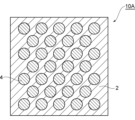
[16] 도전 입자를 함유하는 회로 접속용 접착제 필름으로서, 복수의 상기 도전 입자, 광경화성 성분의 경화물 및 제1 열경화성 성분을 함유하는 제1 접착제층과, 제1 접착제층 상에 마련된, 제2 열경화성 성분을 함유하는 제2 접착제층을 구비하고, 상기 복수의 도전 입자 중 적어도 일부가, 상기 회로 접속용 접착제 필름의 평면시에 있어서, 소정의 패턴으로 나열되고, 또한, 상기 회로 접속용 접착제 필름의 종단면에 있어서, 이웃하는 도전 입자끼리가 서로 이격된 상태로 횡방향으로 나열되어 있는, 회로 접속용 접착제 필름.[16] An adhesive film for circuit connection containing conductive particles, comprising: a first adhesive layer containing a plurality of the conductive particles, a cured product of a photocurable component, and a first thermosetting component; and a first adhesive layer provided on the first adhesive layer. 2 A second adhesive layer containing a thermosetting component is provided, wherein at least some of the plurality of conductive particles are arranged in a predetermined pattern in plan view of the adhesive film for circuit connection, and the adhesive for circuit connection is provided. An adhesive film for circuit connection, wherein, in a longitudinal section of the film, adjacent conductive particles are arranged in a transverse direction while being spaced apart from each other.
본 발명의 다른 일 측면은, 하기 [17]에 나타내는 접속 구조체에 관한 것이다.Another aspect of the present invention relates to a connection structure shown in [17] below.
[17] 제1 전극을 갖는 제1 회로 부재와, 제2 전극을 갖는 제2 회로 부재와, [16]에 기재된 회로 접속용 접착제 필름의 경화체를 포함하고, 상기 제1 전극과 상기 제2 전극을 상기 도전 입자를 개재하여 서로 전기적으로 접속하며 또한 상기 제1 회로 부재와 상기 제2 회로 부재를 접착하는 접속부를 구비하는, 접속 구조체.[17] A first circuit member having a first electrode, a second circuit member having a second electrode, and a cured body of the adhesive film for circuit connection described in [16], wherein the first electrode and the second electrode are included. A connection structure comprising: a connecting portion that electrically connects to each other via the conductive particles and adheres the first circuit member and the second circuit member.
본 발명의 다른 일 측면은, 하기 [18]에 나타내는 접속 구조체의 제조 방법에 관한 것이다.Another aspect of the present invention relates to a method for manufacturing a bonded structure shown in [18] below.
[18] 제1 전극을 갖는 제1 회로 부재의 상기 제1 전극이 마련되어 있는 면과, 제2 전극을 갖는 제2 회로 부재의 상기 제2 전극이 마련되어 있는 면의 사이에, [16]에 기재된 회로 접속용 접착제 필름을 배치하는 것과, 상기 제1 회로 부재와 상기 회로 접속용 접착제 필름과 상기 제2 회로 부재를 포함하는 적층체를 상기 적층체의 두께 방향으로 압압한 상태로 가열함으로써, 상기 제1 전극과 상기 제2 전극을 상기 도전 입자를 개재하여 서로 전기적으로 접속하고 또한 상기 제1 회로 부재와 상기 제2 회로 부재를 접착하는 것을 포함하는, 접속 구조체의 제조 방법.[18] Between the surface provided with the first electrode of the first circuit member having the first electrode and the surface provided with the second electrode of the second circuit member having the second electrode, described in [16], By disposing an adhesive film for circuit connection, and heating a laminate including the first circuit member, the adhesive film for circuit connection, and the second circuit member while being pressed in the thickness direction of the laminate, A method of manufacturing a bonded structure comprising electrically connecting a first electrode and a second electrode to each other via the conductive particles, and bonding the first circuit member and the second circuit member together.
본 발명에 의하면, 도전 입자의 위치 및 개수를 충분히 제어하면서, 대향하는 회로 전극 간에 있어서의 도전 입자의 포착률을 향상시킬 수 있고, 또한, 전극 간의 도통을 충분히 확보할 수 있는 회로 접속용 접착제 필름을 제조하는 방법을 제공할 수 있다.According to the present invention, an adhesive film for circuit connection capable of improving the capture rate of conductive particles between opposing circuit electrodes while sufficiently controlling the position and number of conductive particles and sufficiently securing conduction between the electrodes. A manufacturing method can be provided.
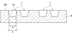
도 1은, 회로 접속용 접착제 필름의 일 실시형태를 나타내는 모식 단면도이다.
도 2는, 도 1의 회로 접속용 접착제 필름에 있어서의 도전 입자의 배치예를 나타내는 모식 평면도이다.
도 3은, 도 1의 회로 접속용 접착제 필름에 있어서의 도전 입자의 배치예를 나타내는 모식 평면도이다.
도 4는, 회로 접속용 접착제 필름의 다른 일 실시형태를 나타내는 모식 단면도이다.
도 5는, 도 1의 회로 접속용 접착제 필름의 제조에 이용되는 기체의 모식 단면도이다.
도 6은, 도 5의 기체의 오목부의 단면 형상의 변형예를 나타내는 도이다.
도 7은, 도 5의 기체의 오목부에 도전 입자가 배치된 상태를 나타내는 도이다.
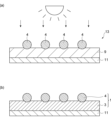
도 8은, 일 실시형태의 회로 접속용 접착제 필름의 제조 방법의 일 공정을 나타내는 모식 단면도이다.
도 9는, 도 1의 회로 접속용 접착제 필름의 제조 방법의 일 공정을 나타내는 모식 단면도이다.
도 10은, 도 1의 회로 접속용 접착제 필름의 제조 방법의 일 공정을 나타내는 모식 단면도이다.
도 11은, 접속 구조체의 일 실시형태를 나타내는 모식 단면도이다.
도 12는, 접속 구조체의 제조 방법의 일 실시형태를 나타내는 모식 단면도이다.1 : is a schematic cross-sectional view which shows one Embodiment of the adhesive film for circuit connection.
FIG. 2 is a schematic plan view showing an example of arrangement of conductive particles in the adhesive film for circuit connection shown in FIG. 1 .
FIG. 3 is a schematic plan view showing an example of arrangement of conductive particles in the adhesive film for circuit connection shown in FIG. 1 .
Fig. 4 is a schematic cross-sectional view showing another embodiment of the adhesive film for circuit connection.
5 : is a schematic cross-sectional view of the base body used for manufacture of the adhesive film for circuit connection of FIG.
Fig. 6 is a diagram showing a modified example of the cross-sectional shape of the concave portion of the body of Fig. 5;
Fig. 7 is a diagram showing a state in which conductive particles are disposed in the concave portions of the base body of Fig. 5;
8 : is a schematic cross-sectional view which shows one process of the manufacturing method of the adhesive film for circuit connection of one Embodiment.
Fig. 9 is a schematic cross-sectional view showing one step of the manufacturing method of the adhesive film for circuit connection shown in Fig. 1 .
Fig. 10 is a schematic cross-sectional view showing one step of the manufacturing method of the adhesive film for circuit connection of Fig. 1 .
11 is a schematic cross-sectional view showing one embodiment of a connection structure.
12 is a schematic cross-sectional view showing one embodiment of a method for manufacturing a bonded structure.
이하, 본 발명의 실시형태에 대하여 설명한다. 단, 본 발명은 이하의 실시형태에 한정되는 것은 아니다. 또한, 이하에서 예시하는 재료는, 특별히 설명하지 않는 한, 1종 단독으로 이용해도 되고, 2종 이상을 조합하여 이용해도 된다. 조성물 중의 각 성분의 함유량은, 조성물 중에 각 성분에 해당하는 물질이 복수 존재하는 경우, 특별히 설명하지 않는 한, 조성물 중에 존재하는 당해 복수의 물질의 합계량을 의미한다. "~"를 이용하여 나타난 수치 범위는, "~"의 전후에 기재되는 수치를 각각 최솟값 및 최댓값으로서 포함하는 범위를 나타낸다. 본 명세서 중에 단계적으로 기재되어 있는 수치 범위에 있어서, 어느 단계의 수치 범위의 상한값 또는 하한값은, 다른 단계의 수치 범위의 상한값 또는 하한값으로 치환해도 된다. 본 명세서 중에 기재되어 있는 수치 범위에 있어서, 그 수치 범위의 상한값 또는 하한값은, 실시예에 나타나 있는 값으로 치환해도 된다. 본 명세서에 있어서, "(메트)아크릴레이트"란, 아크릴레이트, 및, 그에 대응하는 메타크릴레이트 중 적어도 일방을 의미한다. "(메트)아크릴로일" 등의 다른 유사한 표현에 있어서도 동일하다.EMBODIMENT OF THE INVENTION Hereinafter, embodiment of this invention is described. However, this invention is not limited to the following embodiment. In addition, the material illustrated below may be used individually by 1 type, and may be used in combination of 2 or more types, unless there is particular notice. The content of each component in the composition means the total amount of the plurality of substances present in the composition, unless otherwise specified, when a plurality of substances corresponding to each component are present in the composition. A numerical range expressed using "-" represents a range including the numerical values described before and after "-" as the minimum and maximum values, respectively. In the numerical ranges described step by step in this specification, the upper limit or lower limit of the numerical range in one stage may be replaced with the upper limit or lower limit of the numerical range in another stage. In the numerical range described in this specification, the upper limit value or lower limit value of the numerical range may be substituted with the value shown in the Example. In this specification, “(meth)acrylate” means at least one of acrylates and methacrylates corresponding thereto. The same applies to other similar expressions such as "(meth)acryloyl".
<회로 접속용 접착제 필름><Adhesive film for circuit connection>
도 1은, 일 실시형태의 회로 접속용 접착제 필름의 종단면을 모식적으로 나타내는 도이다. 도 1에 나타나는 회로 접속용 접착제 필름(10A)은, 복수의 도전 입자(4)와, 광경화성 성분의 경화물 및 제1 열경화성 성분을 포함하는 접착제 성분(3)을 함유하는 제1 접착제층(1)과, 제1 접착제층(1) 상에 마련된, 제2 열경화성 성분을 함유하는 제2 접착제층(2)을 구비하는 필름상의 접착제(접착제 필름)이다. 본 명세서에 있어서, "종단면"이란, 주면(主面)(예를 들면 회로 접속용 접착제 필름(10A)의 주면)에 대하여 대략 직교하는 단면(두께 방향의 단면)을 의미한다. 또, 제1 열경화성 성분 및 제2 열경화성 성분은, 각각 제1 접착제층 및 제2 접착제층에 함유되는 열경화성 성분을 의미한다.1 : is a figure which shows typically the longitudinal cross section of the adhesive film for circuit connection of one Embodiment. The
복수의 도전 입자(4) 중 적어도 일부는, 회로 접속용 접착제 필름(10A)의 종단면에 있어서, 이웃하는 도전 입자끼리가 서로 이격된 상태로 횡방향으로 나열되어 있다. 환언하면, 회로 접속용 접착제 필름(10A)은, 그 종단면에 있어서, 옆에 위치하는 도전 입자와 이격된 상태의 도전 입자(4)가 횡방향으로 열을 이루고 있는 중앙 영역(10a)과, 도전 입자(4)가 존재하지 않는 표면 측 영역(10b, 10c)에 의하여 구성되어 있다. 여기에서, "횡방향"이란 회로 접속용 접착제 필름의 주면과 대략 평행한 방향(도 1에 있어서의 좌우 방향)을 의미한다. 이웃하는 도전 입자끼리가 서로 이격된 상태로 횡방향으로 나열되어 있는 것은, 예를 들면, 주사(走査)형 전자 현미경 등에 의하여 회로 접속용 접착제 필름의 종단면을 관찰함으로써 확인할 수 있다. 또한, 도 1에서는, 도전 입자(4)의 일부가 제1 접착제층(1)의 표면으로부터 노출(예를 들면, 제2 접착제층(2) 측으로 돌출)되어 있지만, 도전 입자(4)가 제1 접착제층(1)의 표면으로부터 노출되지 않도록, 도전 입자(4)의 전체가 제1 접착제층(1) 중에 매립되어 있어도 된다.At least some of the plurality of
도 2 및 도 3은, 회로 접속용 접착제 필름(10A)에 있어서의 도전 입자(4)의 배치예를 모식적으로 나타내는 평면도이다. 도 2 및 도 3에 나타나는 바와 같이, 복수의 도전 입자(4) 중 적어도 일부는, 회로 접속용 접착제 필름의 평면시에 있어서, 소정의 패턴으로 나열되어 있다. 도 2에서는, 회로 접속용 접착제 필름의 평면시에 있어서, 도전 입자(4)가 회로 접속용 접착제 필름(10A)의 전체의 영역에 대하여 규칙적이고 또한 대략 균등한 간격으로 배치되어 있지만, 예를 들면, 도 3에 나타나는 바와 같이, 회로 접속용 접착제 필름의 평면시에 있어서, 복수의 도전 입자(4)가 규칙적으로 배치되어 있는 영역(10d)과, 도전 입자(4)가 존재하지 않는 영역(10e)이 규칙적으로 형성되도록, 도전 입자(4)가 배치되어 있어도 된다. 도전 입자(4)의 위치 및 개수는, 예를 들면, 접속해야 할 전극의 형상, 사이즈 및 패턴 등에 따라, 설정할 수 있다. 복수의 도전 입자 중 적어도 일부가 소정의 패턴으로 나열되어 있는 것은, 예를 들면, 전자 현미경 등을 이용하여, 회로 접속용 접착제 필름의 주면 상방으로부터 그 회로 접속용 접착제 필름을 관찰함으로써 확인할 수 있다.2 and 3 are plan views schematically illustrating arrangement examples of the
(제1 접착제층)(First adhesive layer)
제1 접착제층(1)은, 도전 입자(4)(이하, "(A) 성분"이라고 하는 경우가 있다.), 광경화성 성분(이하, "(B) 성분"이라고 하는 경우가 있다.)의 경화물 및 제1 열경화성 성분(이하, "(C) 성분"이라고 하는 경우가 있다.)을 함유한다. (B) 성분의 경화물은, (B) 성분을 완전히 경화시킨 경화물이어도 되고, (B) 성분의 일부를 경화시킨 경화물이어도 된다. (C) 성분은, 접속 시에 유동 가능한 성분이며, 예를 들면, 미경화의 경화성 성분(예를 들면 수지 성분)이다. 제1 접착제층(1)을 구성하는 도전 입자(4) 이외의 성분은, 예를 들면, 도전성을 갖지 않는 성분(예를 들면, 절연성 수지 성분)이다.The first
[(A) 성분: 도전 입자][Component (A): conductive particles]
(A) 성분은, 도전성을 갖는 입자이면 특별히 제한되지 않고, Au, Ag, Pd, Ni, Cu, 땜납 등의 금속으로 구성된 금속 입자, 도전성 카본으로 구성된 도전성 카본 입자 등이어도 된다. (A) 성분은, 비도전성의 유리, 세라믹, 플라스틱(폴리스타이렌 등) 등을 포함하는 핵과, 상기 금속 또는 도전성 카본을 포함하고, 핵을 피복하는 피복층을 구비하는 피복 도전 입자여도 된다. (A) 성분은, 1종의 도전 입자를 단독으로 또는 2종 이상의 도전 입자를 조합하여 이용할 수 있다.Component (A) is not particularly limited as long as it is conductive particles, and may be metal particles composed of metals such as Au, Ag, Pd, Ni, Cu, solder, or conductive carbon particles composed of conductive carbon. Component (A) may be coated conductive particles comprising a core made of non-conductive glass, ceramic, plastic (such as polystyrene), and a coating layer containing the metal or conductive carbon covering the core. As the component (A), one type of conductive particle may be used alone or a combination of two or more types of conductive particle may be used.
(A) 성분으로서 피복 도전 입자를 이용하는 경우, 열경화성 성분의 경화물을 가열 또는 가압에 의하여 변형시키는 것이 용이해지기 때문에, 전극끼리를 전기적으로 접속할 때에, 전극과 (A) 성분의 접촉 면적을 증가시켜, 전극 간의 도전성을 보다 향상시킬 수 있다.When using coated conductive particles as component (A), since it becomes easy to deform the cured product of the thermosetting component by heating or pressing, the contact area between the electrode and component (A) is increased when electrically connecting the electrodes. By doing so, the conductivity between the electrodes can be further improved.
(A) 성분으로서 열 용융성의 금속으로 형성된 금속 입자를 이용하는 경우, 전극 간의 접속이 보다 강고해지는 경향이 있다. 이 경향은, (A) 성분으로서 땜납 입자를 이용하는 경우에 현저하다.In the case of using metal particles formed of a hot-meltable metal as the component (A), the connection between the electrodes tends to be stronger. This tendency is remarkable when solder particles are used as component (A).
땜납 입자는, 접속 강도와 저융점의 양립의 관점에서, 주석, 주석 합금, 인듐 및 인듐 합금으로 이루어지는 군으로부터 선택되는 적어도 1종을 포함하고 있어도 된다.The solder particles may contain at least one selected from the group consisting of tin, tin alloy, indium, and indium alloy, from the viewpoint of coexistence of joint strength and low melting point.
주석 합금으로서는, 예를 들면, In-Sn 합금, In-Sn-Ag 합금, Sn-Au 합금, Sn-Bi 합금, Sn-Bi-Ag 합금, Sn-Ag-Cu 합금, Sn-Cu 합금 등을 이용할 수 있다. 이들 주석 합금의 구체예로서는, 하기의 예를 들 수 있다.Examples of tin alloys include In-Sn alloy, In-Sn-Ag alloy, Sn-Au alloy, Sn-Bi alloy, Sn-Bi-Ag alloy, Sn-Ag-Cu alloy, Sn-Cu alloy, etc. available. Specific examples of these tin alloys include the following examples.
·In-Sn(In 52질량%, Sn 48질량% 융점 118℃)In-Sn (52% by mass of In, 48% by mass of Sn, melting point 118°C)
·In-Sn-Ag(In 20질량%, Sn 77.2질량%, Ag 2.8질량% 융점 175℃)In-Sn-Ag (In 20 mass%, Sn 77.2 mass%, Ag 2.8 mass% melting point 175°C)
·Sn-Bi(Sn 43질량%, Bi 57질량% 융점 138℃)・Sn-Bi (43% by mass of Sn, 57% by mass of Bi, melting point 138°C)
·Sn-Bi-Ag(Sn 42질량%, Bi 57질량%, Ag 1질량% 융점 139℃)Sn-Bi-Ag (Sn 42 mass%, Bi 57 mass%,
·Sn-Ag-Cu(Sn 96.5질량%, Ag 3질량%, Cu 0.5질량% 융점 217℃)Sn-Ag-Cu (Sn 96.5 mass%,
·Sn-Cu(Sn 99.3질량%, Cu 0.7질량% 융점 227℃)・Sn-Cu (Sn 99.3 mass%, Cu 0.7 mass% melting point 227°C)
·Sn-Au(Sn 21.0질량%, Au 79.0질량% 융점 278℃)・Sn-Au (Sn 21.0 mass%, Au 79.0 mass% melting point 278°C)
인듐 합금으로서는, 예를 들면, In-Bi 합금, In-Ag 합금 등을 이용할 수 있다. 이들 인듐 합금의 구체예로서는, 하기의 예를 들 수 있다.As an indium alloy, an In-Bi alloy, an In-Ag alloy, etc. can be used, for example. Specific examples of these indium alloys include the following examples.
·In-Bi(In 66.3질량%, Bi 33.7질량% 융점 72℃)In-Bi (In 66.3 mass%, Bi 33.7 mass% melting point 72°C)
·In-Bi(In 33.0질량%, Bi 67.0질량% 융점 109℃)In-Bi (In 33.0 mass%, Bi 67.0 mass% melting point 109°C)
·In-Ag(In 97.0질량%, Ag 3.0질량% 융점 145℃)In-Ag (97.0% by mass of In, 3.0% by mass of Ag, melting point 145°C)
또한, 상술한 주석을 포함하는 인듐 합금은, 주석 합금으로 분류되는 것으로 한다.In addition, the above-mentioned indium alloy containing tin shall be classified as a tin alloy.
땜납 입자는, 고온 고습 시험 시 및 열충격 시험 시에 보다 높은 신뢰성이 얻어지는 관점에서, In-Bi 합금, In-Sn 합금, In-Sn-Ag 합금, Sn-Au 합금, Sn-Bi 합금, Sn-Bi-Ag 합금, Sn-Ag-Cu 합금 및 Sn-Cu 합금으로 이루어지는 군으로부터 선택되는 적어도 1종을 포함해도 된다.Solder particles are In-Bi alloy, In-Sn alloy, In-Sn-Ag alloy, Sn-Au alloy, Sn-Bi alloy, Sn- You may also include at least 1 sort(s) selected from the group which consists of a Bi-Ag alloy, Sn-Ag-Cu alloy, and Sn-Cu alloy.
상기 주석 합금 또는 인듐 합금은, 땜납 입자의 용도(사용 시의 온도) 등에 따라 선택해도 된다. 예를 들면, 저온에서의 융착에 땜납 입자를 이용하는 경우, In-Sn 합금, Sn-Bi 합금을 채용하면, 150℃ 이하에서 융착시킬 수 있다. Sn-Ag-Cu 합금, Sn-Cu 합금 등의 융점이 높은 재료를 채용한 경우, 고온 방치 후에 있어서도 높은 신뢰성을 유지할 수 있다.The tin alloy or indium alloy may be selected according to the purpose of the solder particles (temperature at the time of use) and the like. For example, when solder particles are used for fusion at a low temperature, fusion can be performed at 150°C or less by employing an In-Sn alloy or a Sn-Bi alloy. When a material with a high melting point such as a Sn-Ag-Cu alloy or a Sn-Cu alloy is used, high reliability can be maintained even after being left at a high temperature.
땜납 입자는, Ag, Cu, Ni, Bi, Zn, Pd, Pb, Au, P 및 B로부터 선택되는 1종 이상을 포함해도 된다. 땜납 입자가 Ag 또는 Cu를 포함하는 경우, 땜납 입자의 융점을 220℃ 정도까지 저하시킬 수 있고, 또한, 전극과의 접합 강도가 보다 향상되기 때문에, 보다 양호한 도통 신뢰성이 얻어지기 쉬워진다.The solder particles may contain at least one selected from Ag, Cu, Ni, Bi, Zn, Pd, Pb, Au, P, and B. When the solder particles contain Ag or Cu, the melting point of the solder particles can be lowered to about 220°C, and the bonding strength with the electrode is further improved, so that better conduction reliability can be easily obtained.
땜납 입자의 Cu 함유율은, 예를 들면 0.05~10질량%이며, 0.1~5질량% 또는 0.2~3질량%여도 된다. Cu 함유율이 0.05질량% 이상이면, 보다 양호한 땜납 접속 신뢰성을 달성하기 쉬워진다. 또, Cu 함유율이 10질량% 이하이면, 융점이 낮고, 습윤성이 우수한 땜납 입자가 되기 쉬우며, 결과적으로 땜납 입자에 의한 접합부의 접속 신뢰성이 양호해지기 쉽다.The Cu content of the solder particles is, for example, 0.05 to 10% by mass, and may be 0.1 to 5% by mass or 0.2 to 3% by mass. When the Cu content is 0.05% by mass or more, it becomes easier to achieve better solder connection reliability. In addition, when the Cu content is 10% by mass or less, it is easy to obtain solder particles having a low melting point and excellent wettability, and consequently, the connection reliability of the joint by the solder particles tends to be good.
땜납 입자의 Ag 함유율은, 예를 들면 0.05~10질량%이며, 0.1~5질량% 또는 0.2~3질량%여도 된다. Ag 함유율이 0.05질량% 이상이면, 보다 양호한 땜납 접속 신뢰성을 달성하기 쉬워진다. 또, Ag 함유율이 10질량% 이하이면, 융점이 낮고, 습윤성이 우수한 땜납 입자가 되기 쉬우며, 결과적으로 땜납 입자에 의한 접합부의 접속 신뢰성이 양호해지기 쉽다.The Ag content of the solder particles is, for example, 0.05 to 10% by mass, and may be 0.1 to 5% by mass or 0.2 to 3% by mass. When the Ag content is 0.05% by mass or more, it becomes easier to achieve better solder connection reliability. In addition, when the Ag content is 10% by mass or less, it is easy to obtain solder particles having a low melting point and excellent wettability, and consequently, the connection reliability of the joint by the solder particles tends to be good.
땜납 입자는, 표면의 일부에 평면부를 가져도 된다. 이와 같은 땜납 입자를 이용하는 경우, 땜납 입자가 갖는 평면부가 전극과 접함으로써, 당해 평면부와 전극의 사이에서 넓은 접촉 면적을 확보할 수 있다. 또, 땜납이 젖음 확산되기 쉬운 재료로 형성된 전극과, 땜납이 젖음 확산되기 어려운 재료로 형성된 전극을 접속할 때에, 후자의 전극 측에 땜납 입자의 평면부가 배치되도록 조정함으로써, 양 전극 간의 접속을 적합하게 행할 수 있다. 땜납 입자에 있어서의 상기 평면부 이외의 표면은, 구관(球冠)상이어도 된다. 즉, 땜납 입자는, 평면부와, 구관상의 곡면부를 갖는 것이어도 된다. 구체적으로는, 땜납 입자는, 직경 A를 갖는 구의 표면의 일부에 직경 B의 평면부가 형성된 형상을 갖고 있어도 된다. 이와 같은 땜납 입자를 이용하는 경우, 보다 우수한 도통 신뢰성과 절연 신뢰성이 얻어지기 쉽다.The solder particles may have a flat portion on a part of the surface. In the case of using such solder particles, a large contact area can be secured between the flat portion and the electrode by bringing the flat portion of the solder particle into contact with the electrode. In addition, when connecting an electrode made of a material in which solder is easy to wet-diffuse and an electrode made of a material in which solder does not have wet-diffuse solder, by adjusting so that the flat part of the solder particle is disposed on the side of the latter electrode, the connection between the two electrodes can be suitably made. can do The surface of the solder particle other than the flat portion may be spherical. That is, the solder particles may have a flat portion and a spherical curved portion. Specifically, the solder particle may have a shape in which a flat portion having a diameter B is formed on a part of the surface of a sphere having a diameter A. In the case of using such solder particles, more excellent conduction reliability and insulation reliability are likely to be obtained.
땜납 입자가 직경 A를 갖는 구의 표면의 일부에 직경 B의 평면부가 형성된 형상을 갖는 경우, 보다 우수한 도통 신뢰성 및 절연 신뢰성을 실현하는 관점에서, 땜납 입자의 직경 A에 대한 평면부의 직경 B의 비(B/A)는, 예를 들면 0.01 초과 1.0 미만(0.01<B/A<1.0)이어도 되고, 0.1~0.9여도 된다. 땜납 입자의 직경 A 및 평면부의 직경 B는, 예를 들면 주사형 전자 현미경 등에 의하여 관찰할 수 있다. 구체적으로는, 임의의 땜납 입자를 주사형 전자 현미경에 의하여 관찰하고, 화상을 촬영한다. 얻어진 화상으로부터 땜납 입자의 직경 A 및 평면부의 직경 B를 측정하고, 그 입자의 B/A를 구한다. 이 작업을 300개의 땜납 입자에 대하여 행하여 평균값을 산출하고, 땜납 입자의 B/A로 한다.When the solder particle has a shape in which a flat portion of a diameter B is formed on a part of the surface of a sphere having a diameter A, from the viewpoint of realizing better conduction reliability and insulation reliability, the ratio of the diameter B of the flat portion to the diameter A of the solder particle ( B/A) may be, for example, greater than 0.01 and less than 1.0 (0.01<B/A<1.0), or may be 0.1 to 0.9. The diameter A of the solder particle and the diameter B of the flat portion can be observed, for example, with a scanning electron microscope or the like. Specifically, arbitrary solder particles are observed with a scanning electron microscope and an image is taken. The diameter A of the solder particle and the diameter B of the flat portion are measured from the obtained image, and B/A of the particle is determined. This operation is performed on 300 solder particles to calculate an average value, and this is taken as B/A of the solder particles.
도전 입자의 투영상에 외접하는 사각형을 두 쌍의 평행선에 의하여 작성한 경우에 있어서, 대향하는 변 간의 거리를 각각 X 및 Y(단 Y<X)로 하면, X에 대한 Y의 비(Y/X)는, 0.8 초과 1.0 이하(0.8<Y/X≤1.0)여도 된다. 이와 같은 도전 입자는 보다 진구에 가까운 입자라고 할 수 있다. 도전 입자가 진구에 가까운 형상을 가지면, 후술하는 제조 방법에 있어서 땜납 입자를 기체의 오목부에 수용하기 쉬운 경향이 있다. 또, 도전 입자 중에서도 땜납 입자를 이용하는 경우, 땜납 입자가 진구에 가까운 형상을 가짐으로써, 대향하는 복수의 전극 간을 땜납을 개재하여 전기적으로 접속시킬 때, 땜납 입자와 전극의 접촉에 불균일이 발생하기 어려워, 안정된 접속이 얻어지는 경향이 있다. X에 대한 Y의 비(Y/X)는, 0.8 초과 1.0 미만(0.8<Y/X<1.0)이어도 되고, 0.81~0.99여도 된다. 도전 입자의 투영상은, 예를 들면, 임의의 도전 입자를 주사형 전자 현미경에 의하여 관찰하여 얻을 수 있다. Y/X를 구할 때는, 얻어진 투영상에 대하여 두 쌍의 평행선을 묘화하고, 한 쌍의 평행선은 평행선의 거리가 최소가 되는 위치에, 다른 한 쌍의 평행선은 평행선의 거리가 최대가 되는 위치에 배치한다. 이 작업을 300개의 도전 입자에 대하여 행하여 Y/X의 평균값을 산출하고, 이것을 도전 입자의 Y/X로 한다.In the case where a quadrangle circumscribed on the projected image of the conductive particles is created with two pairs of parallel lines, if the distances between the opposite sides are respectively X and Y (provided that Y<X), the ratio of Y to X (Y/X ) may be greater than 0.8 and less than or equal to 1.0 (0.8<Y/X≤1.0). Such conductive particles can be said to be particles closer to true spheres. If the conductive particles have a shape close to a true sphere, there is a tendency for the solder particles to be easily accommodated in the concave portion of the body in the manufacturing method described later. Also, when solder particles are used among the conductive particles, since the solder particles have a shape close to a true sphere, unevenness occurs in the contact between the solder particles and the electrode when electrically connecting a plurality of opposing electrodes via solder. It is difficult, and a stable connection tends to be obtained. The ratio of Y to X (Y/X) may be greater than 0.8 and less than 1.0 (0.8<Y/X<1.0), or may be 0.81 to 0.99. A projected image of conductive particles can be obtained by, for example, observing arbitrary conductive particles with a scanning electron microscope. When obtaining Y/X, two pairs of parallel lines are drawn on the obtained projection image, one pair of parallel lines is located at the position where the distance between the parallel lines is the minimum, and the other pair of parallel lines is located at the position where the distance between the parallel lines is maximized. place This operation is performed for 300 conductive particles to calculate an average value of Y/X, and this is taken as Y/X of the conductive particles.
(A) 성분은, 상기의 금속 입자, 도전성 카본 입자 또는 피복 도전 입자와, 수지 등의 절연 재료를 포함하고, 그 입자의 표면을 피복하는 절연층을 구비하는 절연 피복 도전 입자여도 된다. (A) 성분이 절연 피복 도전 입자이면, (A) 성분의 함유량이 많은 경우이더라도, 입자의 표면에 절연층을 구비하고 있기 때문에, (A) 성분끼리의 접촉에 의한 단락(短絡)의 발생을 억제할 수 있고, 또, 이웃하는 전극 회로 간의 절연성을 향상시킬 수도 있다.Component (A) may be insulated-coated conductive particles comprising the above-mentioned metal particles, conductive carbon particles or coated conductive particles and an insulating material such as resin, and provided with an insulating layer covering the surface of the particles. If component (A) is insulated-coated conductive particles, even when the content of component (A) is high, since the surface of the particles is provided with an insulating layer, occurrence of short circuit due to contact between components (A) is prevented. can be suppressed, and also the insulation between neighboring electrode circuits can be improved.
(A) 성분의 평균 입자경은, 우수한 도전성이 얻어지기 쉬운 관점에서, 1μm 이상, 2μm 이상 또는 4μm 이상이어도 된다. (A) 성분의 평균 입자경은, 미소 사이즈의 전극에 대하여 보다 양호한 접속 신뢰성이 얻어지기 쉬운 관점에서, 30μm 이하, 25μm 이하 또는 20μm 이하여도 된다. 이들 관점에서, (A) 성분의 평균 입자경은, 1~30μm, 2~25μm 또는 4~20μm여도 된다.The average particle size of component (A) may be 1 μm or more, 2 μm or more, or 4 μm or more from the viewpoint of easily obtaining excellent conductivity. The average particle diameter of component (A) may be 30 μm or less, 25 μm or less, or 20 μm or less from the viewpoint of easily obtaining better connection reliability with respect to micro-sized electrodes. From these viewpoints, the average particle diameter of component (A) may be 1 to 30 μm, 2 to 25 μm, or 4 to 20 μm.
(A) 성분의 평균 입자경은, 사이즈에 맞춘 각종 방법을 이용하여 측정할 수 있다. 예를 들면, 동적 광산란법, 레이저 회절법, 원심 침강법, 전기적 검지대법, 공진식 질량 측정법 등의 방법을 이용할 수 있다. 또한, 광학 현미경, 전자 현미경 등에 의하여 얻어지는 화상으로부터, 입자 사이즈를 측정하는 방법을 이용할 수 있다. 구체적인 장치로서는, 플로식 입자상(像) 분석 장치, 마이크로 트랙, 쿨터 카운터 등을 들 수 있다. 또한, 진구형이 아닌 (A) 성분의 입경은, SEM의 화상에 있어서의 도전 입자에 외접하는 원의 직경이어도 된다.(A) The average particle diameter of component can be measured using various methods matched with size. For example, methods such as a dynamic light scattering method, a laser diffraction method, a centrifugal sedimentation method, an electrical detection method, and a resonance mass measurement method can be used. In addition, a method of measuring the particle size from an image obtained by an optical microscope, an electron microscope or the like can be used. As a specific device, a flow type particle image analyzer, a micro track, a Coulter counter, etc. are mentioned. In addition, the diameter of the non-spherical component (A) may be the diameter of a circle circumscribing the conductive particles in the SEM image.
(A) 성분의 입자경의 C.V.값은, 보다 우수한 도전 신뢰성 및 절연 신뢰성을 실현할 수 있는 관점에서, 20% 이하, 10% 이하, 7% 이하 또는 5% 이하여도 된다. (A) 성분의 입자경의 C.V.값의 하한은 특별히 한정되지 않고, 예를 들면, 0.1% 이상, 1% 이상 또는 2% 이상이어도 된다.The C.V. value of the particle size of the component (A) may be 20% or less, 10% or less, 7% or less, or 5% or less from the viewpoint of realizing better electrical conductivity reliability and insulation reliability. The lower limit of the C.V. value of the particle size of the component (A) is not particularly limited, and may be, for example, 0.1% or more, 1% or more, or 2% or more.
(A) 성분의 입자경의 C.V.값은, 도전 입자의 입자경의 표준 편차를 평균 입자경으로 나눈 값에 100을 곱함으로써 산출된다. 도전 입자의 입자경의 표준 편차는, 상술한 도전 입자의 평균 입자경의 측정 방법과 동일한 방법으로 측정할 수 있다.The C.V. value of the particle diameter of component (A) is calculated by multiplying the value obtained by dividing the standard deviation of the particle diameter of the conductive particles by the average particle diameter by 100. The standard deviation of the particle diameter of the conductive particles can be measured by the same method as the method for measuring the average particle diameter of the conductive particles described above.
(A) 성분은, 평균 입자경이 1~30μm이며, 또한, 입자경의 C.V.값이 20% 이하인 도전 입자여도 된다. 이와 같은 도전 입자는 작은 평균 입자경과 좁은 입도 분포가 양립되어 있고, 도전 신뢰성 및 절연 신뢰성이 높은 이방 도전성 재료에 적용하는 도전 입자로서 적합하게 이용할 수 있다.Component (A) may be conductive particles having an average particle diameter of 1 to 30 µm and a C.V. value of 20% or less of the particle diameter. Such conductive particles have both a small average particle diameter and a narrow particle size distribution, and can be suitably used as conductive particles applied to an anisotropic conductive material having high conductivity reliability and insulation reliability.
(A) 성분의 함유량은, 도전성을 보다 향상시킬 수 있는 관점에서, 제1 접착제층의 전체 질량을 기준으로 하여, 예를 들면, 1질량% 이상, 5질량% 이상 또는 10질량% 이상이어도 된다. (A) 성분의 함유량은, 단락을 억제하기 쉬운 관점에서, 제1 접착제층의 전체 질량을 기준으로 하여, 예를 들면, 80질량% 이하, 70질량% 이하 또는 60질량% 이하여도 된다. 이들 관점에서, (A) 성분의 함유량은, 제1 접착제층의 전체 질량을 기준으로 하여, 예를 들면, 1~80질량%, 5~70질량% 또는 10~60질량%여도 된다.(A) The content of the component may be, for example, 1% by mass or more, 5% by mass or more, or 10% by mass or more based on the total mass of the first adhesive layer from the viewpoint of further improving the conductivity. . The content of component (A) may be, for example, 80% by mass or less, 70% by mass or less, or 60% by mass or less based on the total mass of the first adhesive layer from the viewpoint of easy suppression of short circuit. From these viewpoints, the content of component (A) may be, for example, 1 to 80% by mass, 5 to 70% by mass, or 10 to 60% by mass based on the total mass of the first adhesive layer.
제1 접착제층(1)에 있어서의 (A) 성분의 입자 밀도는, 안정된 접속 저항이 얻어지는 관점에서, 100개/mm2 이상, 1000개/mm2 이상, 3000개/mm2 이상 또는 5000개/mm2 이상이어도 된다. 제1 접착제층(1)에 있어서의 (A) 성분의 입자 밀도는, 이웃하는 전극 간의 절연성을 향상시키는 관점에서, 100000개/mm2 이하, 70000개/mm2 이하, 50000개/mm2 이하 또는 30000개/mm2 이하여도 된다.The particle density of component (A) in the first
[(B) 성분: 광경화성 성분][Component (B): photocurable component]
(B) 성분은, 광조사에 의하여 경화되는 성분(예를 들면 수지 성분)이면 특별히 제한되지 않지만, 접속 저항이 보다 우수한 관점에서, 라디칼 경화성을 갖는 성분이어도 된다. (B) 성분은, 예를 들면, 라디칼 중합성 화합물(이하, "(B1) 성분"이라고 하는 경우가 있다.) 및 광라디칼 중합 개시제(이하, "(B2) 성분"이라고 하는 경우가 있다.)를 포함하고 있어도 된다. (B) 성분은, (B1) 성분 및 (B2) 성분으로 이루어지는 성분일 수 있다.The component (B) is not particularly limited as long as it is a component (for example, a resin component) that is cured by light irradiation, but may be a component having radical curability from the viewpoint of better connection resistance. Component (B) is, for example, a radically polymerizable compound (hereinafter sometimes referred to as “component (B1)”) and an optical radical polymerization initiator (hereinafter sometimes referred to as “component (B2)”). ) may be included. Component (B) may be a component composed of component (B1) and component (B2).
(B1) 성분: 라디칼 중합성 화합물Component (B1): Radical polymerizable compound
(B1) 성분은, 라디칼에 의하여 반응하는 중합성기(라디칼 중합성기)를 갖는 화합물(라디칼 중합성 화합물)이다. 라디칼 중합성기로서는, 예를 들면, (메트)아크릴로일기, 바이닐기, 알릴기, 스타이릴기, 알켄일기, 알켄일렌기, 말레이미드기 등을 들 수 있다. (B1) 성분이 갖는 라디칼 중합성기의 수(관능기 수)는, 중합 후, 원하는 용융 점도가 얻어지기 쉽고, 접속 저항의 저감 효과가 보다 향상되며, 접속 신뢰성이 보다 우수한 관점에서, 2 이상이어도 되고, 중합 시의 경화 수축을 억제하는 관점에서, 10 이하여도 된다. 또, 가교 밀도와 경화 수축의 밸런스를 맞추기 위하여, 라디칼 중합성기의 수가 상기 범위 내에 있는 화합물에 더하여, 라디칼 중합성기의 수가 상기 범위 외에 있는 화합물을 사용해도 된다.Component (B1) is a compound (radical polymerizable compound) having a polymerizable group (radical polymerizable group) that reacts with a radical. As a radical polymerizable group, a (meth)acryloyl group, a vinyl group, an allyl group, a styryl group, an alkenyl group, an alkenylene group, maleimide group etc. are mentioned, for example. The number of radically polymerizable groups (the number of functional groups) of the component (B1) may be 2 or more from the viewpoint of easily obtaining a desired melt viscosity after polymerization, further improving the effect of reducing connection resistance, and further improving connection reliability. , from the viewpoint of suppressing curing shrinkage during polymerization, it may be 10 or less. Further, in order to balance the crosslinking density and curing shrinkage, a compound having a number of radical polymerizable groups outside the above range may be used in addition to a compound having a number of radical polymerizable groups within the above range.
(B1) 성분은, 도전 입자의 유동을 억제하는 관점에서, 예를 들면, 다관능(2관능 이상)의 (메트)아크릴레이트를 포함하고 있어도 된다. 다관능(2관능 이상)의 (메트)아크릴레이트는, 2관능의 (메트)아크릴레이트여도 되고, 2관능의 (메트)아크릴레이트는, 2관능의 방향족 (메트)아크릴레이트여도 된다.The component (B1) may contain, for example, a polyfunctional (bifunctional or higher) (meth)acrylate from the viewpoint of suppressing the flow of conductive particles. A bifunctional (meth)acrylate may be sufficient as the polyfunctional (bifunctional or more functional) (meth)acrylate, and a bifunctional aromatic (meth)acrylate may be sufficient as the bifunctional (meth)acrylate.
다관능의 (메트)아크릴레이트로서는, 예를 들면, 에틸렌글라이콜다이(메트)아크릴레이트, 다이에틸렌글라이콜다이(메트)아크릴레이트, 트라이에틸렌글라이콜다이(메트)아크릴레이트, 테트라에틸렌글라이콜다이(메트)아크릴레이트, 폴리에틸렌글라이콜다이(메트)아크릴레이트, 프로필렌글라이콜다이(메트)아크릴레이트, 다이프로필렌글라이콜다이(메트)아크릴레이트, 트라이프로필렌글라이콜다이(메트)아크릴레이트, 테트라프로필렌글라이콜다이(메트)아크릴레이트, 폴리프로필렌글라이콜다이(메트)아크릴레이트, 에톡시화 폴리프로필렌글라이콜다이(메트)아크릴레이트, 1,3-뷰테인다이올다이(메트)아크릴레이트, 1,4-뷰테인다이올다이(메트)아크릴레이트, 네오펜틸글라이콜다이(메트)아크릴레이트, 3-메틸-1,5-펜테인다이올다이(메트)아크릴레이트, 1,6-헥세인다이올다이(메트)아크릴레이트, 2-뷰틸-2-에틸-1,3-프로페인다이올다이(메트)아크릴레이트, 1,9-노네인다이올다이(메트)아크릴레이트, 1,10-데케인다이올다이(메트)아크릴레이트, 글리세린다이(메트)아크릴레이트, 트라이사이클로데케인다이메탄올(메트)아크릴레이트, 에톡시화 2-메틸-1,3-프로페인다이올다이(메트)아크릴레이트, 트라이메틸올프로페인트라이(메트)아크릴레이트, 에톡시화 트라이메틸올프로페인트라이(메트)아크릴레이트, 프로폭시화 트라이메틸올프로페인트라이(메트)아크릴레이트, 에톡시화 프로폭시화 트라이메틸올프로페인트라이(메트)아크릴레이트, 펜타에리트리톨트라이(메트)아크릴레이트, 에톡시화 펜타에리트리톨트라이(메트)아크릴레이트, 프로폭시화 펜타에리트리톨트라이(메트)아크릴레이트, 에톡시화 프로폭시화 펜타에리트리톨트라이(메트)아크릴레이트, 펜타에리트리톨테트라(메트)아크릴레이트, 에톡시화 펜타에리트리톨테트라(메트)아크릴레이트, 프로폭시화 펜타에리트리톨테트라(메트)아크릴레이트, 에톡시화 프로폭시화 펜타에리트리톨테트라(메트)아크릴레이트, 다이트라이메틸올프로페인테트라아크릴레이트, 다이펜타에리트리톨헥사(메트)아크릴레이트 등의 지방족(메트)아크릴레이트; 에톡시화 비스페놀 A형 다이(메트)아크릴레이트, 프로폭시화 비스페놀 A형 다이(메트)아크릴레이트, 에톡시화 프로폭시화 비스페놀 A형 다이(메트)아크릴레이트, 에톡시화 비스페놀 F형 다이(메트)아크릴레이트, 프로폭시화 비스페놀 F형 다이(메트)아크릴레이트, 에톡시화 프로폭시화 비스페놀 F형 다이(메트)아크릴레이트, 에톡시화 플루오렌형 다이(메트)아크릴레이트(예를 들면, 9,9-바이[4-(2-아크릴로일옥시에톡시)페닐]플루오렌), 프로폭시화 플루오렌형 다이(메트)아크릴레이트, 에톡시화 프로폭시화 플루오렌형 다이(메트)아크릴레이트 등의 방향족 (메트)아크릴레이트; 비스페놀형 에폭시(메트)아크릴레이트, 페놀 노볼락형 에폭시(메트)아크릴레이트, 크레졸 노볼락형 에폭시(메트)아크릴레이트 등의 방향족 에폭시(메트)아크릴레이트; 카프로락톤 변성 트리스-(2-아크릴옥시에틸) 아이소사이아누레이트 등의 아이소사이아누레이트(메트)아크릴레이트 등을 들 수 있다.Examples of the polyfunctional (meth)acrylate include ethylene glycol di(meth)acrylate, diethylene glycol di(meth)acrylate, triethylene glycol di(meth)acrylate, and tetraethylene glycol di(meth)acrylate. Ethylene glycol di(meth)acrylate, polyethylene glycol di(meth)acrylate, propylene glycol di(meth)acrylate, dipropylene glycol di(meth)acrylate, tripropylene glycol Di(meth)acrylate, tetrapropylene glycoldi(meth)acrylate, polypropylene glycoldi(meth)acrylate, ethoxylated polypropylene glycoldi(meth)acrylate, 1,3-view Tanedioldi(meth)acrylate, 1,4-butanedioldi(meth)acrylate, neopentylglycoldi(meth)acrylate, 3-methyl-1,5-pentanedioldi (meth)acrylate, 1,6-hexanedioldi(meth)acrylate, 2-butyl-2-ethyl-1,3-propanedioldi(meth)acrylate, 1,9-nonane Dioldi(meth)acrylate, 1,10-decanedioldi(meth)acrylate, glycerindi(meth)acrylate, tricyclodecanedimethanol(meth)acrylate, ethoxylated 2-methyl- 1,3-propanedioldi(meth)acrylate, trimethylolpropane tri(meth)acrylate, ethoxylated trimethylolpropane tri(meth)acrylate, propoxylated trimethylolpropane tri (meth)acrylate, ethoxylated propoxylated trimethylolpropane tri(meth)acrylate, pentaerythritol tri(meth)acrylate, ethoxylated pentaerythritol tri(meth)acrylate, propoxylated pentaeryth Lithol tri(meth)acrylate, ethoxylated propoxylated pentaerythritol tri(meth)acrylate, pentaerythritol tetra(meth)acrylate, ethoxylated pentaerythritol tetra(meth)acrylate, propoxylated pentaeryth Aliphatic (meth)acrylates such as ritol tetra(meth)acrylate, ethoxylated propoxylated pentaerythritol tetra(meth)acrylate, ditrimethylolpropane tetraacrylate, and dipentaerythritol hexa(meth)acrylate rate; Ethoxylated bisphenol A type di(meth)acrylate, propoxylated bisphenol A type di(meth)acrylate, ethoxylated bisphenol A type di(meth)acrylate, ethoxylated bisphenol F type di(meth)acrylate rate, propoxylated bisphenol F-type di(meth)acrylate, ethoxylated propoxylated bisphenol F-type di(meth)acrylate, ethoxylated fluorene-type di(meth)acrylate (e.g., 9,9- Aromatics such as bi[4-(2-acryloyloxyethoxy)phenyl]fluorene), propoxylated fluorene type di(meth)acrylate, ethoxylated propoxylated fluorene type di(meth)acrylate, etc. (meth)acrylate; aromatic epoxy (meth)acrylates such as bisphenol-type epoxy (meth)acrylate, phenol novolak-type epoxy (meth)acrylate, and cresol novolac-type epoxy (meth)acrylate; Isocyanurate (meth)acrylates, such as caprolactone modified tris-(2-acryloxyethyl) isocyanurate, etc. are mentioned.
다관능(2관능 이상)의 (메트)아크릴레이트의 함유량은, 접속 저항의 저감 효과와 입자 유동의 억제를 양립시키는 관점에서, (B1) 성분의 전체 질량을 기준으로 하여, 예를 들면, 40~100질량%, 50~100질량% 또는 60~100질량%여도 된다.The content of the polyfunctional (bifunctional or higher) (meth)acrylate is, for example, 40 -100 mass %, 50-100 mass %, or 60-100 mass % may be sufficient.
(B1) 성분은, 다관능(2관능 이상)의 (메트)아크릴레이트에 더하여, 단관능의 (메트)아크릴레이트를 더 포함하고 있어도 된다. 단관능의 (메트)아크릴레이트로서는, 예를 들면, (메트)아크릴산; 메틸(메트)아크릴레이트, 에틸(메트)아크릴레이트, 뷰틸(메트)아크릴레이트, 아이소뷰틸(메트)아크릴레이트, tert-뷰틸(메트)아크릴레이트, 뷰톡시에틸(메트)아크릴레이트, 아이소아밀(메트)아크릴레이트, 헥실(메트)아크릴레이트, 2-에틸헥실(메트)아크릴레이트, 헵틸(메트)아크릴레이트, 옥틸헵틸(메트)아크릴레이트, 노닐(메트)아크릴레이트, 데실(메트)아크릴레이트, 2-하이드록시에틸(메트)아크릴레이트, 2-하이드록시프로필(메트)아크릴레이트, 3-클로로-2-하이드록시프로필(메트)아크릴레이트, 2-하이드록시뷰틸(메트)아크릴레이트, 메톡시폴리에틸렌글라이콜(메트)아크릴레이트, 에톡시폴리에틸렌글라이콜(메트)아크릴레이트, 메톡시폴리프로필렌글라이콜(메트)아크릴레이트, 에톡시폴리프로필렌글라이콜(메트)아크릴레이트, 모노(2-(메트)아크릴로일옥시에틸)석시네이트 등의 지방족 (메트)아크릴레이트; 벤질(메트)아크릴레이트, 페닐(메트)아크릴레이트, o-바이페닐(메트)아크릴레이트, 1-나프틸(메트)아크릴레이트, 2-나프틸(메트)아크릴레이트, 페녹시에틸(메트)아크릴레이트, p-큐밀페녹시에틸(메트)아크릴레이트, o-페닐페녹시에틸(메트)아크릴레이트, 1-나프톡시에틸(메트)아크릴레이트, 2-나프톡시에틸(메트)아크릴레이트, 페녹시폴리에틸렌글라이콜(메트)아크릴레이트, 노닐페녹시폴리에틸렌글라이콜(메트)아크릴레이트, 페녹시폴리프로필렌글라이콜(메트)아크릴레이트, 2-하이드록시-3-페녹시프로필(메트)아크릴레이트, 2-하이드록시-3-(o-페닐페녹시)프로필(메트)아크릴레이트, 2-하이드록시-3-(1-나프톡시)프로필(메트)아크릴레이트, 2-하이드록시-3-(2-나프톡시)프로필(메트)아크릴레이트, 비스페놀 A형 에폭시(메트)아크릴레이트 등의 방향족 (메트)아크릴레이트; 글리시딜(메트)아크릴레이트 등의 에폭시기를 갖는 (메트)아크릴레이트, 3,4-에폭시사이클로헥실메틸(메트)아크릴레이트 등의 지환식 에폭시기를 갖는 (메트)아크릴레이트, (3-에틸옥세탄-3-일)메틸(메트)아크릴레이트 등의 옥세탄일기를 갖는 (메트)아크릴레이트 등을 들 수 있다.The component (B1) may further contain a monofunctional (meth)acrylate in addition to the polyfunctional (bifunctional or higher) (meth)acrylate. Examples of the monofunctional (meth)acrylate include (meth)acrylic acid; Methyl (meth)acrylate, ethyl (meth)acrylate, butyl (meth)acrylate, isobutyl (meth)acrylate, tert-butyl (meth)acrylate, butoxyethyl (meth)acrylate, isoamyl ( meth)acrylate, hexyl(meth)acrylate, 2-ethylhexyl(meth)acrylate, heptyl(meth)acrylate, octylheptyl(meth)acrylate, nonyl(meth)acrylate, decyl(meth)acrylate , 2-hydroxyethyl (meth) acrylate, 2-hydroxypropyl (meth) acrylate, 3-chloro-2-hydroxypropyl (meth) acrylate, 2-hydroxybutyl (meth) acrylate, Toxypolyethylene glycol (meth)acrylate, ethoxypolyethylene glycol (meth)acrylate, methoxypolypropylene glycol (meth)acrylate, ethoxypolypropylene glycol (meth)acrylate, mono aliphatic (meth)acrylates such as (2-(meth)acryloyloxyethyl)succinate; Benzyl(meth)acrylate, phenyl(meth)acrylate, o-biphenyl(meth)acrylate, 1-naphthyl(meth)acrylate, 2-naphthyl(meth)acrylate, phenoxyethyl(meth)acrylate Acrylate, p-cumylphenoxyethyl (meth)acrylate, o-phenylphenoxyethyl (meth)acrylate, 1-naphthoxyethyl (meth)acrylate, 2-naphthoxyethyl (meth)acrylate, phenoxy Polyethylene glycol (meth)acrylate, nonylphenoxypolyethylene glycol (meth)acrylate, phenoxypolypropylene glycol (meth)acrylate, 2-hydroxy-3-phenoxypropyl (meth)acrylate Acrylate, 2-hydroxy-3-(o-phenylphenoxy)propyl(meth)acrylate, 2-hydroxy-3-(1-naphthoxy)propyl(meth)acrylate, 2-hydroxy-3 -Aromatic (meth)acrylates such as (2-naphthoxy)propyl (meth)acrylate and bisphenol A epoxy (meth)acrylate; (meth)acrylates having an epoxy group such as glycidyl (meth)acrylate, (meth)acrylates having an alicyclic epoxy group such as 3,4-epoxycyclohexylmethyl (meth)acrylate, and (3-ethyloxa) (meth)acrylates having an oxetanyl group, such as cetan-3-yl)methyl (meth)acrylate; and the like.
단관능의 (메트)아크릴레이트의 함유량은, (B1) 성분의 전체 질량을 기준으로 하여, 예를 들면, 0~60질량%, 0~50질량% 또는 0~40질량%여도 된다.The content of the monofunctional (meth)acrylate may be, for example, 0 to 60% by mass, 0 to 50% by mass, or 0 to 40% by mass based on the total mass of the component (B1).
(B) 성분의 경화물은, 예를 들면, 라디칼 이외에 의하여 반응하는 중합성기를 갖고 있어도 된다. 라디칼 이외에 의하여 반응하는 중합성기는, 예를 들면, 양이온에 의하여 반응하는 양이온 중합성기여도 된다. 양이온 중합성기로서는, 예를 들면, 글리시딜기 등의 에폭시기, 에폭시사이클로헥실메틸기 등의 지환식 에폭시기, 에틸옥세탄일메틸기 등의 옥세탄일기 등을 들 수 있다. 라디칼 이외에 의하여 반응하는 중합성기를 갖는 (B) 성분의 경화물은, 예를 들면, 에폭시기를 갖는 (메트)아크릴레이트, 지환식 에폭시기를 갖는 (메트)아크릴레이트, 옥세탄일기를 갖는 (메트)아크릴레이트 등의 라디칼 이외에 의하여 반응하는 중합성기를 갖는 (메트)아크릴레이트를 (B) 성분으로서 사용함으로써 도입할 수 있다.(B) The hardened|cured material of component may have a polymeric group which reacts by other than a radical, for example. The polymerizable group that reacts by means other than a radical may be, for example, a cationic polymerizable group that reacts by means of a cation. Examples of the cationic polymerizable group include oxetanyl groups such as epoxy groups such as glycidyl groups, alicyclic epoxy groups such as epoxycyclohexylmethyl groups, and ethyloxetanylmethyl groups. The cured product of component (B) having a polymerizable group that reacts by means other than a radical includes, for example, (meth)acrylate having an epoxy group, (meth)acrylate having an alicyclic epoxy group, and (meth)acrylate having an oxetanyl group. It can be introduced by using (meth)acrylates having polymerizable groups other than radicals such as acrylates as component (B).
라디칼 이외에 의하여 반응하는 중합성기를 갖는 (메트)아크릴레이트로서는, 라디칼 중합성 화합물과 후술하는 열경화성 성분을 가교하여, 접속 시에 보다 강고한 접속부를 형성하는 관점에서는, 하기 식 (1)로 나타나는 화합물을 이용해도 된다.As the (meth)acrylate having a polymerizable group that reacts by means other than a radical, a compound represented by the following formula (1) from the viewpoint of crosslinking a radical polymerizable compound and a thermosetting component described later to form a stronger connection portion at the time of connection. You can also use
[화학식 5][Formula 5]

식 (1) 중, R1은, 수소 원자 또는 메틸기를 나타내고, X는 탄소수 1~3의 알케인다이일기를 나타낸다. 탄소수 1~3의 알케인다이일기로서는, 예를 들면, 메틸렌기, 에틸렌기, 프로필렌기 등을 들 수 있다. 상기 식 (1)로 나타나는 화합물의 구체예로서는, 3,4-에폭시사이클로헥실메틸(메트)아크릴레이트를 들 수 있다.In Formula (1), R 1 represents a hydrogen atom or a methyl group, and X represents an alkanediyl group having 1 to 3 carbon atoms. As a C1-C3 alkanediyl group, a methylene group, an ethylene group, a propylene group etc. are mentioned, for example. As a specific example of the compound represented by said Formula (1), 3, 4- epoxycyclohexylmethyl (meth)acrylate is mentioned.
라디칼 이외에 의하여 반응하는 중합성기를 갖는 라디칼 중합성 화합물(예를 들면 (메트)아크릴레이트)은, 중합 시의 경화 수축을 억제하는 관점에서는, 라디칼 이외에 의하여 반응하는 중합성기를 갖지 않는 라디칼 중합성 화합물(예를 들면 (메트)아크릴레이트)과 병용해도 된다. (B1) 성분의 전체 질량에 대한 라디칼 이외에 의하여 반응하는 중합성기를 갖는 라디칼 중합성 화합물의 질량비(라디칼 이외에 의하여 반응하는 중합성기를 갖는 라디칼 중합성 화합물의 질량(도입량)/(B1) 성분의 전체 질량(도입량))는, 신뢰성 향상의 관점에서, 예를 들면, 0 이상, 0.1 이상, 0.2 이상 또는 0.3 이상이어도 되고, 0.7 이하, 0.6 이하, 0.5 이하 또는 0.4 이하여도 되며, 0~0.7, 0.1~0.6, 0.2~0.5 또는 0.3~0.4여도 된다. 중합 시의 경화 수축을 보다 억제하는 관점에서는, 라디칼 이외에 의하여 반응하는 중합성기를 갖지 않는 (메트)아크릴레이트에 대한, 라디칼 이외에 의하여 반응하는 중합성기를 갖는 (메트)아크릴레이트의 질량비가 상기 범위여도 된다.A radically polymerizable compound (for example, (meth)acrylate) having a polymerizable group that reacts by other than a radical is a radically polymerizable compound that does not have a polymerizable group that reacts by other than a radical, from the viewpoint of suppressing cure shrinkage during polymerization. You may use it together with (for example, (meth)acrylate). (B1) Mass ratio of the radically polymerizable compound having a polymerizable group that reacts by other than a radical to the total mass of the component (mass of the radically polymerizable compound having a polymerizable group that reacts by other than a radical (introduced amount) / (B1) Total amount of the component The mass (leading amount) may be, for example, 0 or more, 0.1 or more, 0.2 or more, or 0.3 or more, or 0.7 or less, 0.6 or less, 0.5 or less, or 0.4 or less, or 0 to 0.7 or 0.1, from the viewpoint of improving reliability. -0.6, 0.2-0.5, or 0.3-0.4 may be sufficient. From the viewpoint of further suppressing cure shrinkage during polymerization, even if the mass ratio of (meth)acrylate having a polymerizable group that reacts other than a radical to (meth)acrylate that does not have a polymerizable group that reacts by other than a radical is within the above range, do.
(B1) 성분은, 다관능(2관능 이상) 및 단관능의 (메트)아크릴레이트에 더하여, 그 외의 라디칼 중합성 화합물을 포함하고 있어도 된다. 그 외의 라디칼 중합성 화합물로서는, 예를 들면, 말레이미드 화합물, 바이닐에터 화합물, 알릴 화합물, 스타이렌 유도체, 아크릴아마이드 유도체, 나드이미드 유도체 등을 들 수 있다. 그 외의 라디칼 중합성 화합물의 함유량은, (B1) 성분의 전체 질량을 기준으로 하여, 예를 들면, 0~40질량%여도 된다.The component (B1) may contain other radically polymerizable compounds in addition to polyfunctional (bifunctional or more) and monofunctional (meth)acrylates. Examples of other radically polymerizable compounds include maleimide compounds, vinyl ether compounds, allyl compounds, styrene derivatives, acrylamide derivatives, and nadimide derivatives. The content of the other radically polymerizable compounds may be, for example, 0 to 40% by mass based on the total mass of the component (B1).
(B2) 성분: 광라디칼 중합 개시제Component (B2): Photoradical polymerization initiator
(B2) 성분은, 150~750nm의 범위 내의 파장을 포함하는 광, 바람직하게는 254~405nm의 범위 내의 파장을 포함하는 광, 더 바람직하게는 365nm의 파장을 포함하는 광(예를 들면 자외광)의 조사에 의하여 라디칼을 발생시키는 광중합 개시제(광잠재성 라디칼 발생제)이다. (B2) 성분은, 1종을 단독으로 이용해도 되고, 복수를 조합하여 이용해도 된다.Component (B2) is light having a wavelength within a range of 150 to 750 nm, preferably light having a wavelength within a range of 254 to 405 nm, and more preferably light having a wavelength of 365 nm (for example, ultraviolet light). ) It is a photopolymerization initiator (photolatent radical generator) that generates radicals by irradiation. (B2) component may be used individually by 1 type, and may be used combining plurality.
(B2) 성분은, 광에 의하여 분해되어 유리(遊離) 라디칼을 발생시킨다. 즉, (B2) 성분은, 외부로부터의 광에너지의 부여에 의하여 라디칼을 발생시키는 화합물이다. (B2) 성분은, 옥심에스터 구조, 비스이미다졸 구조, 아크리딘 구조, α-아미노알킬페논 구조, 아미노벤조페논 구조, N-페닐글라이신 구조, 아실포스핀옥사이드 구조, 벤질다이메틸케탈 구조, α-하이드록시알킬페논 구조 등의 구조를 갖는 화합물이어도 된다. (B2) 성분은, 1종을 단독으로 이용해도 되고, 복수를 조합하여 이용해도 된다.Component (B2) is decomposed by light to generate free radicals. That is, component (B2) is a compound that generates radicals by application of light energy from the outside. (B2) component is an oxime ester structure, a biimidazole structure, an acridine structure, an α-aminoalkylphenone structure, an aminobenzophenone structure, an N-phenylglycine structure, an acylphosphine oxide structure, a benzyldimethylketal structure, It may be a compound having a structure such as an α-hydroxyalkylphenone structure. (B2) component may be used individually by 1 type, and may be used combining plurality.
(B2) 성분은, 도전 입자의 유동을 더 억제하고, 포착률을 더 향상시키는 관점, 및, 접속 후의 박리를 더 억제하며, 접속 저항의 상승을 더 억제하는 관점에서는, 옥심에스터 구조를 갖는 화합물이어도 된다. 동일한 관점에서, 옥심에스터 구조를 갖는 화합물은, 하기 식 (I)로 나타나는 화합물이어도 된다.Component (B2) may be a compound having an oxime ester structure from the viewpoint of further suppressing the flow of conductive particles and further improving the capture rate, further suppressing separation after connection, and further suppressing an increase in connection resistance. do. From the same viewpoint, the compound represented by the following formula (I) may be sufficient as the compound which has an oxime ester structure.
[화학식 6][Formula 6]

식 (I) 중, R2, R3 및 R4는, 각각 독립적으로, 수소 원자, 탄소수 1~20의 알킬기 또는 방향족계 탄화 수소기를 포함하는 유기기를 나타낸다.In formula (I), R 2 , R 3 and R 4 each independently represent a hydrogen atom, an alkyl group having 1 to 20 carbon atoms, or an organic group containing an aromatic hydrocarbon group.
옥심에스터 구조를 갖는 화합물의 구체예로서는, 1-페닐-1,2-뷰테인다이온-2-(o-메톡시카보닐)옥심, 1-페닐-1,2-프로페인다이온-2-(o-메톡시카보닐)옥심, 1-페닐-1,2-프로페인다이온-2-(o-에톡시카보닐)옥심, 1-페닐-1,2-프로페인다이온-2-o-벤조일옥심, 1,3-다이페닐프로페인트라이온-2-(o-에톡시카보닐)옥심, 1-페닐-3-에톡시프로페인트라이온-2-(o-벤조일)옥심, 1,2-옥테인다이온, 1-[4-(페닐싸이오)페닐-, 2-(o-벤조일옥심)], 에탄온, 1-[9-에틸-6-(2-메틸벤조일)-9H-카바졸-3-일]-, 1-(o-아세틸옥심) 등을 들 수 있다. 이와 같은 고활성인 옥심에스터계의 광라디칼 중합 개시제를 이용하는 경우, (B1) 성분물의 배합량이 적은 경우에도 충분히 가교를 진행시킬 수 있다.Specific examples of the compound having an oxime ester structure include 1-phenyl-1,2-butanedione-2-(o-methoxycarbonyl)oxime, 1-phenyl-1,2-propanedione-2- (o-methoxycarbonyl)oxime, 1-phenyl-1,2-propanedione-2-(o-ethoxycarbonyl)oxime, 1-phenyl-1,2-propanedione-2- o-benzoyloxime, 1,3-diphenylpropanetrione-2-(o-ethoxycarbonyl)oxime, 1-phenyl-3-ethoxypropanetrione-2-(o-benzoyl)oxime, 1, 2-octanedione, 1-[4-(phenylthio)phenyl-, 2-(o-benzoyloxime)], ethanone, 1-[9-ethyl-6-(2-methylbenzoyl)-9H -carbazol-3-yl]-, 1-(o-acetyloxime), etc. are mentioned. In the case of using such a highly active oxime ester-based photo-radical polymerization initiator, crosslinking can be sufficiently promoted even when the compounding amount of the component (B1) is small.
(B2) 성분의 함유량은, 도전 입자의 유동 억제의 관점에서, (B1) 성분 100질량부에 대하여, 예를 들면, 0.1~10질량부, 0.3~7질량부 또는 0.5~5질량부여도 된다.The content of component (B2) may be, for example, 0.1 to 10 parts by mass, 0.3 to 7 parts by mass, or 0.5 to 5 parts by mass, based on 100 parts by mass of component (B1), from the viewpoint of suppressing the flow of conductive particles. .
(B) 성분의 경화물의 함유량은, 도전 입자의 유동을 억제하는 관점에서, 제1 접착제층 중의 (A) 성분 이외의 성분의 합계량 100질량부에 대하여, 예를 들면, 1질량부 이상, 5질량부 이상 또는 10질량부 이상이어도 된다. (B) 성분의 경화물의 함유량은, 저압 실장에 있어서 저저항을 발현시키는 관점에서, 제1 접착제층 중의 (A) 성분 이외의 성분의 합계량 100질량부에 대하여, 예를 들면, 30질량부 이하, 25질량부 이하 또는 20질량부 이하여도 된다. 이들 관점에서, (B) 성분의 경화물의 함유량은, 제1 접착제층 중의 (A) 성분 이외의 성분의 합계량 100질량부에 대하여, 예를 들면, 1~30질량부, 5~25질량부 또는 10~20질량부여도 된다. 또한, 제1 접착제층을 형성하기 위한 조성물 또는 조성물층 중의 (B) 성분의 함유량(조성물 또는 조성물층의 전체 질량 기준)은 상기 범위와 동일해도 된다.From the viewpoint of suppressing the flow of conductive particles, the content of the cured product of component (B) is, for example, 1 part by mass or more, 5 parts by mass, based on 100 parts by mass of the total amount of components other than component (A) in the first adhesive layer. It may be more than 10 parts by mass or more than 10 parts by mass. The content of the cured product of the component (B) is, for example, 30 parts by mass or less with respect to 100 parts by mass of the total amount of components other than the component (A) in the first adhesive layer, from the viewpoint of developing low resistance in low-voltage mounting. , 25 parts by mass or less or 20 parts by mass or less may be sufficient. From these viewpoints, the content of the cured product of component (B) is, for example, 1 to 30 parts by mass, 5 to 25 parts by mass, or 100 parts by mass of the total amount of components other than component (A) in the first adhesive layer. 10 to 20 mass may be imparted. In addition, the composition for forming the first adhesive layer or the content of component (B) in the composition layer (based on the total mass of the composition or composition layer) may be the same as the above range.
[(C) 성분: 열경화성 성분][Component (C): thermosetting component]
(C) 성분은, 열에 의하여 경화하는 성분(예를 들면 수지 성분)이면 특별히 제한되지 않지만, (B) 성분이 라디칼 경화성을 갖는 성분인 경우, 보관 안정성 등의 관점에서, (C) 성분은, 라디칼 경화성을 갖지 않는 성분이어도 된다. (B) 성분이 라디칼 경화성을 갖는 성분이고, 또한, (C) 성분도 라디칼 경화성을 갖는 성분인 경우, 보관 시에 제1 접착제층 중에 잔류한 라디칼에 의하여 열경화성 성분의 경화가 진행될 가능성이 있다. 라디칼 경화성을 갖지 않는 성분으로서는, 양이온 경화성을 갖는 성분(예를 들면, 양이온 중합성 화합물 및 열양이온 중합 개시제) 및 음이온 경화성을 갖는 성분(음이온 중합성 화합물 및 열음이온 중합 개시제)을 들 수 있다.Component (C) is not particularly limited as long as it is a component that is cured by heat (for example, a resin component), but when component (B) is a component having radical curability, from the viewpoint of storage stability, etc., component (C) is, A component that does not have radical curability may be used. When component (B) is a component having radical curability and component (C) is also a component having radical curability, curing of the thermosetting component may proceed due to radicals remaining in the first adhesive layer during storage. Examples of components not having radical curability include components having cation curability (e.g., cationically polymerizable compounds and thermal cationic polymerization initiators) and components having anionic curability (anionic polymerizable compounds and thermal anionic polymerization initiators).
(C) 성분은, 접속 저항이 보다 우수한 관점에서는, 양이온 경화성을 갖는 성분이어도 되고, 예를 들면, 양이온 중합성 화합물(이하, "(C1) 성분"이라고 하는 경우가 있다.) 및 열양이온 중합 개시제(이하, "(C2) 성분"이라고 하는 경우가 있다.)를 포함하고 있어도 된다. (C) 성분은, (C1) 성분 및 (C2) 성분만으로 이루어지는 성분일 수 있다.(C) Component may be a component having cationic curing properties from the viewpoint of better connection resistance, for example, a cationically polymerizable compound (hereinafter sometimes referred to as "component (C1)") and thermal cationic polymerization. It may contain an initiator (hereinafter sometimes referred to as "component (C2)"). Component (C) may be a component consisting only of component (C1) and component (C2).
(C1) 성분: 양이온 중합성 화합물(C1) component: cationic polymerizable compound
(C1) 성분은, 열에 의하여 (C2) 성분과 반응함으로써 가교하는 화합물이다. 또한, (C1) 성분은, 라디칼 중합성기를 갖지 않는 화합물을 의미하고, (C1) 성분은, (B1) 성분에 포함되지 않는다. (C1) 성분은, 1종을 단독으로 이용해도 되고, 복수를 조합하여 이용해도 된다.Component (C1) is a compound that crosslinks by reacting with component (C2) by heat. In addition, the component (C1) means a compound having no radical polymerizable group, and the component (C1) is not included in the component (B1). (C1) Component may be used individually by 1 type, and may be used combining plurality.
(C1) 성분은, 접속 저항의 저감 효과가 더 향상되고, 접속 신뢰성이 보다 우수한 관점에서, 환상 에터기를 갖는 화합물이어도 된다. 환상 에터기를 갖는 화합물 중에서도, 옥세테인 화합물 및 지환식 에폭시 화합물로 이루어지는 군으로부터 선택되는 적어도 1종을 이용하는 경우, 접속 저항의 저감 효과가 한층 향상되는 경향이 있다. (C1) 성분은, 원하는 용융 점도가 얻어지기 쉬운 관점에서, 옥세테인 화합물의 적어도 1종 및 지환식 에폭시 화합물의 적어도 1종의 양방을 포함하고 있어도 된다.The component (C1) may be a compound having a cyclic ether group from the viewpoint of further improving the reduction effect of connection resistance and further improving connection reliability. Among the compounds having a cyclic ether group, when at least one selected from the group consisting of oxetane compounds and alicyclic epoxy compounds is used, the effect of reducing connection resistance tends to be further improved. (C1) Component may contain both at least 1 sort(s) of at least 1 sort(s) of an oxetane compound, and at least 1 sort(s) of an alicyclic epoxy compound from a viewpoint of being easy to obtain a desired melt viscosity.
(C1) 성분으로서의 옥세테인 화합물은, 옥세탄일기를 갖고, 또한 라디칼 중합성기를 갖지 않는 화합물이면 특별히 제한 없이 사용할 수 있다. 옥세테인 화합물의 시판품으로서는, 예를 들면, ETERNACOLL OXBP(상품명, 4,4'-비스[(3-에틸-3-옥세탄일)메톡시메틸]바이페닐, 우베 고산 주식회사제), OXSQ, OXT-121, OXT-221, OXT-101, OXT-212(상품명, 도아 고세이 주식회사제) 등을 들 수 있다. 이들은, 1종의 화합물을 단독으로 이용해도 되고, 복수를 조합하여 이용해도 된다.The oxetane compound as component (C1) can be used without particular limitation as long as it is a compound having an oxetanyl group and not having a radical polymerizable group. Examples of commercially available products of the oxetane compound include ETERNACOLL OXBP (trade name, 4,4'-bis[(3-ethyl-3-oxetanyl)methoxymethyl]biphenyl, manufactured by Ube Kosan Co., Ltd.), OXSQ, and OXT. -121, OXT-221, OXT-101, OXT-212 (trade name, manufactured by Toagosei Co., Ltd.) and the like. These may be used individually as 1 type of compound, and may be used combining plurality.
(C1) 성분으로서의 지환식 에폭시 화합물은, 지환식 에폭시기(예를 들면, 에폭시사이클로헥실기)를 갖고, 또한 라디칼 중합성기를 갖지 않는 화합물이면 특별히 제한 없이 사용할 수 있다. 지환식 에폭시 화합물의 시판품으로서는, 셀록사이드 8010(상품명, 바이-7-옥사바이사이클로[4.1.0]헵테인, 주식회사 다이셀제) 외, 예를 들면, EHPE3150, EHPE3150CE, 셀록사이드 2021P, 셀록사이드 2081(상품명, 주식회사 다이셀제) 등을 들 수 있다. 이들은, 1종의 화합물을 단독으로 이용해도 되고, 복수를 조합하여 이용해도 된다. (C1) 성분으로서는, 비스페놀 A형 에폭시 수지, 비스페놀 F형 에폭시 수지 등의 방향족계 탄화 수소기를 갖는 에폭시 화합물(예를 들면, 미쓰비시 가가쿠 주식회사제의 상품명 "jER1010", "YL983U" 등)을 이용할 수도 있다. 방향족계 탄화 수소기를 갖는 에폭시 화합물은, 접속 저항의 저감 효과가 더 향상되고, 접속 신뢰성이 보다 우수한 관점에서, 지환식 에폭시 화합물과 조합하여 이용해도 된다.As the alicyclic epoxy compound as component (C1), any compound having an alicyclic epoxy group (eg, epoxycyclohexyl group) and not having a radical polymerizable group can be used without particular limitation. As a commercial item of an alicyclic epoxy compound, Celoxide 8010 (brand name, bi-7-oxabicyclo [4.1.0] heptane, Daicel Co., Ltd. product) others, for example, EHPE3150, EHPE3150CE, Celoxide 2021P, Celoxide 2081 (Brand name, Daicel Co., Ltd. product) etc. are mentioned. These may be used individually as 1 type of compound, and may be used combining plurality. As the component (C1), an epoxy compound having an aromatic hydrocarbon group such as a bisphenol A type epoxy resin or a bisphenol F type epoxy resin (for example, trade names "jER1010" and "YL983U" manufactured by Mitsubishi Chemical Corporation) may be used. may be An epoxy compound having an aromatic hydrocarbon group may be used in combination with an alicyclic epoxy compound from the viewpoint of further improving the reduction effect of connection resistance and further improving connection reliability.
(C2) 성분: 열양이온 중합 개시제(C2) Component: Thermal Cationic Polymerization Initiator
(C2) 성분은, 가열에 의하여 산 등을 발생시켜 중합을 개시하는 열중합 개시제(열잠재성 양이온 발생제)이다. (C2) 성분은 양이온과 음이온으로 구성되는 염 화합물이어도 된다. (C2) 성분은, 예를 들면, BF4 -, BR4 -(R은, 2 이상의 불소 원자 또는 2 이상의 트라이플루오로메틸기로 치환된 페닐기를 나타낸다.), PF6 -, SbF6 -, AsF6 - 등의 음이온을 갖는, 설포늄염, 포스포늄염, 암모늄염, 다이아조늄염, 아이오도늄염, 아닐리늄염, 피리디늄염 등의 오늄염 등을 들 수 있다. 이들은, 1종을 단독으로 이용해도 되고, 복수를 조합하여 이용해도 된다.Component (C2) is a thermal polymerization initiator (thermal latent cation generator) that initiates polymerization by generating an acid or the like by heating. (C2) Component may be a salt compound composed of a cation and an anion. Component (C2) includes, for example, BF 4 - , BR 4 - (R represents a phenyl group substituted with two or more fluorine atoms or two or more trifluoromethyl groups), PF 6 - , SbF 6 - , AsF and onium salts such as sulfonium salts, phosphonium salts, ammonium salts, diazonium salts, iodonium salts, anilinium salts, and pyridinium salts having anions such as 6- . These may be used individually by 1 type, and may be used combining plurality.
(C2) 성분은, 속(速)경화성의 관점에서, 예를 들면, 구성 원소로서 붕소를 포함하는 음이온을 갖는 염 화합물이어도 된다. 이와 같은 염 화합물로서는, 예를 들면, BF4 - 또는 BR4 -(R은, 2 이상의 불소 원자 또는 2 이상의 트라이플루오로메틸기로 치환된 페닐기를 나타낸다.)를 갖는 염 화합물을 들 수 있다. 구성 원소로서 붕소를 포함하는 음이온은, BR4 -여도 되고, 보다 구체적으로는, 테트라키스(펜타플루오로페닐)보레이트여도 된다.Component (C2) may be, for example, a salt compound having an anion containing boron as a constituent element from the viewpoint of quick curability. Examples of such a salt compound include a salt compound having BF 4 - or BR 4 - (R represents a phenyl group substituted with two or more fluorine atoms or two or more trifluoromethyl groups.). The anion containing boron as a constituent element may be BR 4 - , and more specifically, may be tetrakis(pentafluorophenyl)borate.
(C2) 성분은, 보존 안정성의 관점에서, 하기 식 (II) 또는 하기 식 (III)으로 나타나는 양이온을 갖는 염 화합물이어도 된다.(C2) Component may be a salt compound having a cation represented by the following formula (II) or the following formula (III) from the viewpoint of storage stability.
[화학식 7][Formula 7]

[화학식 8][Formula 8]

식 (II) 중, R5 및 R6은, 각각 독립적으로, 수소 원자, 탄소수 1~20의 알킬기 또는 치환기를 갖거나 혹은 무치환의 방향족계 탄화 수소기를 포함하는 유기기를 나타내고, R7은, 탄소수 1~6의 알킬기를 나타낸다.In formula (II), R 5 and R 6 each independently represent a hydrogen atom, an alkyl group having 1 to 20 carbon atoms, or an organic group having a substituent or containing an unsubstituted aromatic hydrocarbon group, and R 7 is, Represents an alkyl group having 1 to 6 carbon atoms.
식 (II)로 나타나는 양이온을 갖는 염 화합물은, 보존 안정성과 저온 활성의 양립 관점에서, 방향족 설포늄염 화합물(방향족 설포늄염형 열산발생제)이어도 된다. 즉, 식 (II)에 있어서의 R5 및 R6 중 적어도 일방이 치환기를 갖거나 혹은 무치환의 방향족계 탄화 수소기를 포함하는 유기기여도 된다. 식 (II)로 나타나는 양이온을 갖는 염 화합물에 있어서의 음이온은, 구성 원소로서 안티모니를 포함하는 음이온이어도 되고, 예를 들면, 헥사플루오로안티모네이트(헥사플루오로안티모니산)여도 된다.The salt compound having a cation represented by Formula (II) may be an aromatic sulfonium salt compound (aromatic sulfonium salt type thermal acid generator) from the viewpoint of both storage stability and low-temperature activity. That is, at least one of R 5 and R 6 in formula (II) may be an organic group having a substituent or containing an unsubstituted aromatic hydrocarbon group. The anion in the salt compound having a cation represented by Formula (II) may be an anion containing antimony as a constituent element, and may be, for example, hexafluoroantimonate (hexafluoroantimony acid).
식 (II)로 나타나는 양이온을 갖는 화합물의 구체예로서는, 1-나프틸메틸-p-하이드록시페닐설포늄헥사플루오로안티모네이트(산신 가가쿠 주식회사제, SI-60 주제) 등을 들 수 있다.Specific examples of the compound having a cation represented by formula (II) include 1-naphthylmethyl-p-hydroxyphenylsulfonium hexafluoroantimonate (manufactured by Sanshin Chemical Co., Ltd., SI-60 Co., Ltd.) and the like. .
식 (III) 중, R8 및 R9는, 각각 독립적으로, 수소 원자, 탄소수 1~20의 알킬기 또는 치환기를 갖거나 혹은 무치환의 방향족계 탄화 수소기를 포함하는 유기기를 나타내고, R10 및 R11은, 각각 독립적으로, 탄소수 1~6의 알킬기를 나타낸다.In formula (III), R 8 and R 9 each independently represent a hydrogen atom, an alkyl group having 1 to 20 carbon atoms or an organic group having a substituent or containing an unsubstituted aromatic hydrocarbon group, and R 10 and R 11 represents a C1-C6 alkyl group each independently.
식 (III)으로 나타나는 양이온을 갖는 염 화합물(제4급 암모늄염형 열산발생제)은, 양이온 경화에 대한 경화 저해를 일으킬 수 있는 물질에 대한 내성을 갖는 점에서, 예를 들면, 아닐리늄염 화합물이어도 된다. 즉, 식 (III)에 있어서의 R8 및 R9 중 적어도 일방이 치환기를 갖거나 혹은 무치환의 방향족계 탄화 수소기를 포함하는 유기기여도 된다. 아닐리늄염 화합물로서는, 예를 들면, N,N-다이메틸아닐리늄염, N,N-다이에틸아닐리늄염 등의 N,N-다이알킬아닐리늄염 등을 들 수 있다. 식 (III)으로 나타나는 양이온을 갖는 염 화합물에 있어서의 음이온은, 구성 원소로서 붕소를 포함하는 음이온이어도 되고, 예를 들면, 테트라키스(펜타플루오로페닐)보레이트여도 된다.Since the salt compound (quaternary ammonium salt type thermal acid generator) having a cation represented by Formula (III) has resistance to substances that may cause curing inhibition with respect to cation curing, for example, an anilinium salt compound may be continued That is, at least one of R 8 and R 9 in Formula (III) may be an organic group having a substituent or containing an unsubstituted aromatic hydrocarbon group. Examples of the anilinium salt compound include N,N-dialkylanilinium salts such as N,N-dimethylanilinium salts and N,N-diethylanilinium salts. The anion containing boron as a constituent element may be sufficient as the anion in the salt compound which has a cation represented by Formula (III), and tetrakis (pentafluorophenyl) borate may be sufficient as it, for example.
식 (III)으로 나타나는 양이온을 갖는 화합물은, 구성 원소로서 붕소를 포함하는 음이온을 갖는 아닐리늄염이어도 된다. 이와 같은 염 화합물의 시판품으로서는, 예를 들면, CXC-1821(상품명, King Industries사제) 등을 들 수 있다.The compound having a cation represented by Formula (III) may be an anilinium salt having an anion containing boron as a constituent element. As a commercial item of such a salt compound, CXC-1821 (a brand name, made by King Industries) etc. is mentioned, for example.
(C2) 성분의 함유량은, 제1 접착제층을 형성하기 위한 접착제 필름의 형성성 및 경화성을 담보하는 관점에서, (C1) 성분 100질량부에 대하여, 예를 들면, 0.1~20질량부, 1~18질량부, 3~15질량부 또는 5~12질량부여도 된다.The content of the component (C2) is, for example, 0.1 to 20 parts by mass, 1 to 100 parts by mass of the component (C1), from the viewpoint of securing the formability and curability of the adhesive film for forming the first adhesive layer. 18 parts by mass, 3 to 15 parts by mass, or 5 to 12 parts by mass may be provided.
(C) 성분의 함유량은, 제1 접착제층을 형성하기 위한 접착제 필름의 경화성을 담보하는 관점에서, 제1 접착제층 중의 (A) 성분 이외의 성분의 합계량 100질량부에 대하여, 예를 들면, 5질량부 이상, 10질량부 이상, 15질량부 이상 또는 20질량부 이상이어도 된다. (C) 성분의 함유량은, 제1 접착제층을 형성하기 위한 접착제 필름의 형성성을 담보하는 관점에서, 제1 접착제층 중의 (A) 성분 이외의 성분의 합계량 100질량부에 대하여, 예를 들면, 70질량부 이하, 60질량부 이하, 50질량부 이하 또는 40질량부 이하여도 된다. 이들 관점에서, (C) 성분의 함유량은, 제1 접착제층 중의 (A) 성분 이외의 성분의 합계량 100질량부에 대하여, 예를 들면, 5~70질량부, 10~60질량부, 15~50질량부 또는 20~40질량부여도 된다. 또한, 조성물 또는 조성물층 중의 (C) 성분의 함유량(조성물 또는 조성물층의 전체 질량 기준)은 상기 범위와 동일해도 된다.The content of component (C) is, from the viewpoint of ensuring the curability of the adhesive film for forming the first adhesive layer, with respect to 100 parts by mass of the total amount of components other than component (A) in the first adhesive layer, for example, It may be 5 parts by mass or more, 10 parts by mass or more, 15 parts by mass or more, or 20 parts by mass or more. The content of the component (C) is, from the viewpoint of ensuring the formability of the adhesive film for forming the first adhesive layer, with respect to 100 parts by mass of the total amount of components other than the component (A) in the first adhesive layer, for example , 70 parts by mass or less, 60 parts by mass or less, 50 parts by mass or less, or 40 parts by mass or less may be sufficient. From these viewpoints, the content of the component (C) is, for example, 5 to 70 parts by mass, 10 to 60 parts by mass, 15 to 60 parts by mass, based on 100 parts by mass of the total amount of components other than the component (A) in the first adhesive layer. You may provide 50 mass parts or 20-40 mass parts. In addition, the content of component (C) in the composition or composition layer (based on the total mass of the composition or composition layer) may be the same as the above range.
[그 외의 성분][Other Ingredients]
제1 접착제층(1)은, (A) 성분, (B) 성분의 경화물, 및 (C) 성분 이외에 그 외의 성분을 더 함유하고 있어도 된다. 그 외의 성분으로서는, 예를 들면, 열가소성 수지(이하, "(D) 성분"이라고 하는 경우가 있다.), 커플링제(이하, "(E) 성분"이라고 하는 경우가 있다.), 및, 충전재(이하, "(F) 성분"이라고 하는 경우가 있다.) 등을 들 수 있다.The 1st
(D) 성분으로서는, 예를 들면, 페녹시 수지, 폴리에스터 수지, 폴리아마이드 수지, 폴리유레테인 수지, 폴리에스터유레테인 수지, 아크릴 고무, 에폭시 수지(25℃에서 고형) 등을 들 수 있다. 이들은, 1종을 단독으로 이용해도 되고, 복수를 조합하여 이용해도 된다. (B) 성분 및 (C) 성분을 함유하는 조성물이 (D) 성분을 더 함유함으로써, 당해 조성물로부터 조성물층(나아가서는 제1 접착제층(1))을 용이하게 형성할 수 있다. 상기 페녹시 수지로서는, 예를 들면, 플루오렌형 페녹시 수지, 비스페놀 A·비스페놀 F 공중합형 페녹시 수지 등을 들 수 있다.Examples of the component (D) include phenoxy resins, polyester resins, polyamide resins, polyurethane resins, polyester urethane resins, acrylic rubbers, and epoxy resins (solid at 25°C). there is. These may be used individually by 1 type, and may be used combining plurality. When the composition containing the component (B) and the component (C) further contains the component (D), the composition layer (and, by extension, the first adhesive layer 1) can be easily formed from the composition. As said phenoxy resin, a fluorene type phenoxy resin, bisphenol A-bisphenol F copolymerization type phenoxy resin, etc. are mentioned, for example.
(D) 성분의 중량 평균 분자량(Mw)은, 실장 시의 수지 배제성의 관점에서, 예를 들면, 5000~200000, 10000~100000, 20000~80000 또는 40000~60000이어도 된다. 또한, Mw는, 젤 퍼미에이션 크로마토그래피(GPC)로 측정하고, 표준 폴리스타이렌에 의한 검량선을 이용하여 환산한 값을 의미한다.The weight average molecular weight (Mw) of component (D) may be, for example, 5000 to 200000, 10000 to 100000, 20000 to 80000, or 40000 to 60000 from the viewpoint of resin exclusion property at the time of mounting. In addition, Mw means the value measured by gel permeation chromatography (GPC) and converted using the calibration curve by standard polystyrene.
(D) 성분의 함유량은, 제1 접착제층 중의 (A) 성분 이외의 성분의 합계량 100질량부에 대하여, 예를 들면, 1질량부 이상, 5질량부 이상, 10질량부 이상 또는 20질량부 이상이어도 되고, 70질량부 이하, 60질량부 이하, 50질량부 이하 또는 40질량부 이하여도 되며, 1~70질량부, 5~60질량부, 10~50질량부 또는 20~40질량부여도 된다. 또한, 제1 접착제층을 형성하기 위한 조성물 또는 조성물층 중의 (D) 성분의 함유량(조성물 또는 조성물층의 전체 질량 기준)은 상기 범위와 동일해도 된다.The content of the component (D) is, for example, 1 part by mass or more, 5 parts by mass or more, 10 parts by mass or more, or 20 parts by mass with respect to 100 parts by mass of the total amount of components other than the component (A) in the first adhesive layer. It may be more than 70 parts by mass, 60 parts by mass or less, 50 parts by mass or less, or 40 parts by mass or less, and may be 1 to 70 parts by mass, 5 to 60 parts by mass, 10 to 50 parts by mass, or 20 to 40 parts by mass. do. In addition, the composition for forming the first adhesive layer or the content of component (D) in the composition layer (based on the total mass of the composition or composition layer) may be the same as the above range.
(E) 성분으로서는, 예를 들면, (메트)아크릴로일기, 머캅토기, 아미노기, 이미다졸기, 에폭시기 등의 유기 관능기를 갖는 실레인 커플링제(γ-글리시독시프로필트라이메톡시실레인 등), 테트라알콕시실레인 등의 실레인 화합물, 테트라알콕시타이타네이트 유도체, 폴리다이알킬타이타네이트 유도체 등을 들 수 있다. 이들은, 1종을 단독으로 이용해도 되고, 복수를 조합하여 이용해도 된다. 제1 접착제층(1)이 (E) 성분을 함유함으로써, 접착성을 더 향상시킬 수 있다. (E) 성분은, 예를 들면, 실레인 커플링제여도 된다.As component (E), for example, a silane coupling agent (γ-glycidoxypropyltrimethoxysilane, etc.) having organic functional groups such as (meth)acryloyl group, mercapto group, amino group, imidazole group, epoxy group ), silane compounds such as tetraalkoxysilane, tetraalkoxy titanate derivatives, and polydialkyl titanate derivatives. These may be used individually by 1 type, and may be used combining plurality. Adhesiveness can further be improved because the 1st
(E) 성분의 함유량은, 제1 접착제층 중의 (A) 성분 이외의 성분의 합계량 100질량부에 대하여, 예를 들면, 0.1~10질량부여도 된다. 또한, 제1 접착제층을 형성하기 위한 조성물 또는 조성물층 중의 (E) 성분의 함유량(조성물 또는 조성물층의 전체 질량 기준)은 상기 범위와 동일해도 된다.The content of the component (E) may be, for example, 0.1 to 10 parts by mass relative to 100 parts by mass of the total amount of components other than the component (A) in the first adhesive layer. In addition, the composition for forming the first adhesive layer or the content of component (E) in the composition layer (based on the total mass of the composition or composition layer) may be the same as the above range.
(F) 성분으로서는, 예를 들면, 비도전성의 필러(예를 들면, 비도전 입자)를 들 수 있다. (F) 성분은, 무기 필러 및 유기 필러 중 어느 것이어도 된다. 무기 필러로서는, 예를 들면, 실리카 미립자, 알루미나 미립자, 실리카-알루미나 미립자, 타이타니아 미립자, 지르코니아 미립자 등의 금속 산화물 미립자; 금속 질화물 미립자 등의 무기 미립자를 들 수 있다. 유기 필러로서는, 예를 들면, 실리콘 미립자, 메타크릴레이트·뷰타다이엔·스타이렌 미립자, 아크릴·실리콘 미립자, 폴리아마이드 미립자, 폴리이미드 미립자 등의 유기 미립자를 들 수 있다. 이들은, 1종을 단독으로 이용해도 되고, 복수를 조합하여 이용해도 된다. (F) 성분은, 예를 들면, 실리카 미립자여도 된다. (F) 성분의 함유량은, 제1 접착제층 중의 (A) 성분 이외의 성분의 합계량 100질량부에 대하여, 예를 들면, 0.1~10질량부여도 된다. 또한, 제1 접착제층을 형성하기 위한 조성물 또는 조성물층 중의 (F) 성분의 함유량(조성물 또는 조성물층의 전체 질량 기준)은 상기 범위와 동일해도 된다.(F) As a component, a non-conductive filler (for example, non-conductive particle) is mentioned, for example. (F) Component may be any of an inorganic filler and an organic filler. Examples of the inorganic filler include metal oxide fine particles such as silica fine particles, alumina fine particles, silica-alumina fine particles, titania fine particles, and zirconia fine particles; and inorganic fine particles such as metal nitride fine particles. Examples of the organic filler include organic fine particles such as silicon fine particles, methacrylate/butadiene/styrene fine particles, acryl/silicon fine particles, polyamide fine particles, and polyimide fine particles. These may be used individually by 1 type, and may be used combining plurality. (F) Component may be silica fine particles, for example. The content of the component (F) may be, for example, 0.1 to 10 parts by mass relative to 100 parts by mass of the total amount of components other than the component (A) in the first adhesive layer. In addition, the composition for forming the first adhesive layer or the content of component (F) in the composition layer (based on the total mass of the composition or composition layer) may be the same as the above range.
제1 접착제층(1)은, 그 외의 성분으로서, 연화제, 촉진제, 열화 방지제, 착색제, 난연화제, 틱소트로픽제 등의 그 외의 첨가제를 더 함유하고 있어도 된다. 그 외의 첨가제의 함유량은, 제1 접착제층 중의 (A) 성분 이외의 성분의 합계량 100질량부에 대하여, 예를 들면, 0.1~10질량부여도 된다. 또한, 제1 접착제층을 형성하기 위한 조성물 또는 조성물층 중의 그 외의 첨가제의 함유량(조성물 또는 조성물층의 전체 질량 기준)은 상기 범위와 동일해도 된다.The first
제1 접착제층(1)의 두께(d1)는, 회로 접속용 접착제 필름의 제조 시에 있어서의 도전 입자(4)의 전사성의 관점에서, 예를 들면, 0.5μm 이상, 1.0μm 이상 또는 2.0μm 이상이어도 된다. 제1 접착제층(1)의 두께(d1)는, 접속 시에 도전 입자를 보다 더 효율적으로 포착할 수 있는 관점에서, 예를 들면, 5.0μm 이하, 4.0μm 이하 또는 3.0μm 이하여도 된다. 이들 관점에서, 제1 접착제층(1)의 두께(d1)는, 예를 들면, 0.5~5.0μm, 1.0~4.0μm 또는 2.0~3.0μm여도 된다. 또한, 도 1에 나타나는 바와 같이, 도전 입자(4)의 일부가 제1 접착제층(1)의 표면으로부터 노출(예를 들면, 제2 접착제층(2) 측으로 돌출)되어 있는 경우, 제1 접착제층(1)에 있어서의 제2 접착제층(2) 측과는 반대 측의 면(1a)부터, 이웃하는 도전 입자(4, 4)의 이간(離間) 부분에 위치하는 제1 접착제층(1)과 제2 접착제층(2)의 경계(S)까지의 거리(도 1에 있어서 d1로 나타내는 거리)가 제1 접착제층(1)의 두께이며, 도전 입자(4)의 노출 부분은 제1 접착제층(1)의 두께에는 포함되지 않는다.The thickness d1 of the first
제1 접착제층(1)의 두께(d1)는, 예를 들면, 접착제 필름을 2매의 유리(두께: 1mm 정도) 사이에 끼워 넣고, 비스페놀 A형 에폭시 수지(상품명: jER811, 미츠비시 케미컬 주식회사제) 100g과, 경화제(상품명: 에포마운트 경화제, 리파인텍 주식회사제) 10g으로 이루어지는 수지 조성물로 주형(注型) 후에, 연마기를 이용하여 단면 연마를 행하며, 주사형 전자 현미경(SEM, 상품명: SE-8020, 주식회사 히타치 하이테크 사이언스제)을 이용하여 측정함으로써 구할 수 있다.The thickness d1 of the first
<제2 접착제층><Second adhesive layer>
제2 접착제층(2)은, 예를 들면, 도전성을 갖지 않는 성분(절연성 수지 성분)으로 구성되어 있는 절연성 접착제층이다. 제2 접착제층(2)은, 적어도 (C) 성분을 함유한다.The second
제2 접착제층(2)에 있어서의 (C) 성분(즉, 제2 열경화성 성분)에 포함되는 성분(예를 들면, (C1) 성분, (C2) 성분 등)의 상세(종류, 조합 등)는, 제1 접착제층(1)에 있어서의 (C) 성분(즉, 제1 열경화성 성분)에 포함되는 성분의 상세와 동일한 점에서, 여기에서는 상세한 설명은 생략한다. 제2 열경화성 성분은, 제1 열경화성 성분과 동일해도 되고, 상이해도 된다.Details (type, combination, etc.) of the components (eg, (C1) component, (C2) component, etc.) contained in the (C) component (ie, the second thermosetting component) in the second
(C) 성분의 함유량은, 신뢰성을 유지하는 관점에서, 제2 접착제층의 전체 질량을 기준으로 하여, 예를 들면, 5질량% 이상, 10질량% 이상, 15질량% 이상 또는 20질량% 이상이어도 된다. (C) 성분의 함유량은, 공급 형태의 일 양태인 릴에 있어서의 수지 번짐 트러블을 방지하는 관점에서, 제2 접착제층의 전체 질량을 기준으로 하여, 예를 들면, 70질량% 이하, 60질량% 이하, 50질량% 이하 또는 40질량% 이하여도 된다. 이들 관점에서, (C) 성분의 함유량은, 제2 접착제층의 전체 질량을 기준으로 하여, 예를 들면, 5~70질량%, 10~15질량%, 15~50질량% 또는 20~40질량%여도 된다.From the viewpoint of maintaining reliability, the content of component (C) is, for example, 5% by mass or more, 10% by mass or more, 15% by mass or more, or 20% by mass or more based on the total mass of the second adhesive layer. may be continued The content of component (C) is, for example, 70% by mass or less, 60% by mass, based on the total mass of the second adhesive layer, from the viewpoint of preventing resin bleeding trouble in the reel, which is one aspect of the supply mode. % or less, 50 mass % or less, or 40 mass % or less may be sufficient. From these points of view, the content of component (C) is, for example, 5 to 70% by mass, 10 to 15% by mass, 15 to 50% by mass, or 20 to 40% by mass based on the total mass of the second adhesive layer. may be %.
제2 접착제층(2)은, 제1 접착제층(1)에 있어서의 그 외의 성분((D) 성분, (E) 성분, (F) 성분 및 그 외의 첨가제 등)을 더 함유하고 있어도 된다. 그 외의 성분의 바람직한 양태는, 제1 접착제층(1)의 바람직한 양태와 동일하다.The second
(D) 성분의 함유량은, 제2 접착제층의 전체 질량을 기준으로 하여, 예를 들면, 1질량% 이상, 5질량% 이상 또는 10질량% 이상이어도 되고, 80질량% 이하, 60질량% 이하 또는 40질량% 이하여도 되며, 1~80질량%, 5~60질량% 또는 10~40질량%여도 된다.The content of component (D) is, for example, 1% by mass or more, 5% by mass or more, or 10% by mass or more, based on the total mass of the second adhesive layer, 80% by mass or less, 60% by mass or less Alternatively, it may be 40% by mass or less, and may be 1 to 80% by mass, 5 to 60% by mass, or 10 to 40% by mass.
(E) 성분의 함유량은, 제2 접착제층의 전체 질량을 기준으로 하여, 예를 들면, 0.1~10질량%여도 된다.(E) The content of the component may be, for example, 0.1 to 10% by mass based on the total mass of the second adhesive layer.
(F) 성분의 함유량은, 제2 접착제층의 전체 질량을 기준으로 하여, 예를 들면, 1질량% 이상, 10질량% 이상 또는 30질량% 이상이어도 되고, 90질량% 이하, 70질량% 이하 또는 50질량% 이하여도 되며, 1~90질량% 이하, 10~70질량% 이하 또는 30~50질량%여도 된다.The content of component (F) is, for example, 1% by mass or more, 10% by mass or more, or 30% by mass or more, based on the total mass of the second adhesive layer, 90% by mass or less, 70% by mass or less Alternatively, it may be 50% by mass or less, 1 to 90% by mass or less, 10 to 70% by mass or less, or 30 to 50% by mass.
그 외의 첨가제의 함유량은, 제2 접착제층의 전체 질량을 기준으로 하여, 예를 들면, 0.1~10질량%여도 된다.The content of the other additives may be, for example, 0.1 to 10% by mass based on the total mass of the second adhesive layer.
제2 접착제층(2)의 두께(d2)는, 접속하는 회로 부재의 전극의 높이 등에 따라 적절히 설정해도 된다. 제2 접착제층(2)의 두께(d2)는, 전극 간의 스페이스를 충분히 충전하여 전극을 밀봉할 수 있고, 보다 양호한 접속 신뢰성이 얻어지는 관점에서, 예를 들면, 2μm 이상, 5μm 이상 또는 10μm 이상이어도 되고, 30μm 이하, 20μm 이하 또는 15μm 이하여도 되며, 2~30μm, 5~20μm 또는 10~15μm여도 된다. 또한, 도 1에 나타나는 바와 같이, 도전 입자(4)의 일부가 제1 접착제층(1)의 표면으로부터 노출(예를 들면, 제2 접착제층(2) 측으로 돌출)되어 있는 경우, 제2 접착제층(2)에 있어서의 제1 접착제층(1) 측과는 반대 측의 면(2a)부터, 이웃하는 도전 입자(4, 4)의 이간 부분에 위치하는 제1 접착제층(1)과 제2 접착제층(2)의 경계(S)까지의 거리(도 1에 있어서 d2로 나타내는 거리)가 제2 접착제층(2)의 두께이다. 제2 접착제층(2)의 두께(d2)는, 예를 들면, 상술한 제1 접착제층(1)의 두께(d1)의 측정 방법과 동일하게 하여 구할 수 있다.You may set the thickness d2 of the 2nd
회로 접속용 접착제 필름(10A)의 두께(회로 접속용 접착제 필름(10A)을 구성하는 모든 층의 두께의 합계)는, 예를 들면, 2.5μm 이상, 6μm 이상 또는 12μm 이상이어도 되고, 35μm 이하, 24μm 이하 또는 18μm 이하여도 되며, 2.5~35μm, 6~24μm 또는 12~24μm여도 된다.The thickness of the
회로 접속용 접착제 필름(10A)은, 회로의 접속에 이용되는 접착제 필름이다. 회로 접속용 접착제 필름(10A)은, 이방 도전성을 갖고 있어도 되고, 이방 도전성을 갖고 있지 않아도 된다. 즉, 회로 접속용 접착제 필름은, 이방 도전성의 접착제 필름이어도 되고, 비이방 도전성(예를 들면 등방 도전성)의 접착제 필름이어도 된다. 회로 접속용 접착제 필름(10A)은, 제1 전극을 갖는 제1 회로 부재의 당해 제1 전극이 마련되어 있는 면과, 제2 전극을 갖는 제2 회로 부재의 당해 제2 전극이 마련되어 있는 면의 사이에 배치되고, 제1 회로 부재와 회로 접속용 접착제 필름(10A)과 제2 회로 부재를 포함하는 적층체를 적층체의 두께 방향으로 압압한 상태로 가열함으로써, 제1 전극과 제2 전극을 도전 입자(혹은 도전 입자의 용융 고화물)를 개재하여 서로 전기적으로 접속하며 또한 제1 회로 부재와 제2 회로 부재를 접착하기 위하여 이용되어도 된다. 또한, 상술한 "이방 도전성"이란, 가압 방향으로는 도통하고, 비가압 방향으로는 절연성을 유지한다는 의미이다.10 A of adhesive films for circuit connections are adhesive films used for connection of circuits. 10 A of adhesive films for circuit connections may or may not have anisotropic conductivity. That is, the adhesive film for circuit connection may be an anisotropic conductive adhesive film or a non-anisotropic conductive (for example, isotropic conductive) adhesive film. 10 A of adhesive film for circuit connections between the surface provided with the said 1st electrode of the 1st circuit member which has a 1st electrode, and the surface provided with the said 2nd electrode of the 2nd circuit member which has a 2nd electrode , and the first electrode and the second electrode are electrically conductive by heating the laminated body including the first circuit member, the circuit connection
회로 접속용 접착제 필름(10A)에 의하면, 열경화성 성분에 의하여 접속 시의 수지의 배제성을 확보하면서, 광경화성 성분의 경화물에 의하여 접속 시의 도전 입자의 유동성을 억제하고, 접속되는 전극 간에 있어서의 도전 입자의 포착률을 향상시킬 수 있다. 그 때문에, 회로 접속용 접착제 필름(10A)에 의하면, 쇼트의 발생이 적고, 또, 전극 간의 도통성도 우수한 접속 구조체를 얻을 수 있다.According to the
이상, 일 실시형태의 회로 접속용 접착제 필름에 대하여 설명했지만, 본 발명은 상기 실시형태에 한정되지 않는다.As mentioned above, although the adhesive film for circuit connection of one embodiment was demonstrated, this invention is not limited to the said embodiment.
회로 접속용 접착제 필름은, 예를 들면, 도 4에 나타나는 회로 접속용 접착제 필름(10B)과 같이, 제1 접착제층(1)의 제2 접착제층(2)과는 반대 측에 (C) 성분(열경화성 성분)을 함유하는 제3 접착제층(5)을 구비하고 있어도 된다. 제3 접착제층(5)은, 예를 들면, 도전성을 갖지 않는 성분(절연성 수지 성분)으로 구성되어 있는 절연성 접착제층이다. 회로 접속용 접착제 필름(10B)은, 제3 접착제층(5)이 적층되어 있는 것 이외에는, 회로 접속용 접착제 필름(10A)과 동일한 구성을 갖는다.The adhesive film for circuit connection is component (C) on the side opposite to the second
제3 접착제층(5)에 함유되는 (C) 성분(이하, "제3 열경화성 성분"이라고도 한다.)의 상세는, 상술한 열경화성 성분과 동일하다. 예를 들면, 제3 열경화성 성분은, (C1) 성분(즉, 양이온 중합성 화합물) 및 (C2) 성분(즉, 열양이온 중합 개시제)을 포함하고 있어도 된다. 제3 열경화성 성분에서 사용되는 (C1) 성분 및 (C2) 성분은, 제1 열경화성 성분에서 사용되는 (C1) 성분 및 (C2) 성분과 동일한 점에서, 여기에서는 상세한 설명은 생략한다. 제3 열경화성 성분은, 제1 열경화성 성분과 동일해도 되고, 상이해도 된다. 제3 열경화성 성분은, 제2 열경화성 성분과 동일해도 되고, 상이해도 된다.Details of component (C) contained in the third adhesive layer 5 (hereinafter, also referred to as "third thermosetting component") are the same as those of the thermosetting component described above. For example, the 3rd thermosetting component may contain the (C1) component (namely, cationically polymerizable compound) and the (C2) component (namely, thermal cation polymerization initiator). Since components (C1) and (C2) used in the third thermosetting component are the same as components (C1) and (C2) used in the first thermosetting component, detailed descriptions are omitted here. The third thermosetting component may be the same as or different from the first thermosetting component. The third thermosetting component may be the same as or different from the second thermosetting component.
(C) 성분의 함유량은, 양호한 전사성 및 내박리성을 부여하는 관점에서, 제3 접착제층의 전체 질량을 기준으로 하여, 예를 들면, 5질량% 이상, 10질량% 이상, 15질량% 이상 또는 20질량% 이상이어도 된다. (C) 성분의 함유량은, 양호한 하프 커팅성 및 내블로킹성(릴의 수지 번짐 억제)을 부여하는 관점에서, 제3 접착제층의 전체 질량을 기준으로 하여, 예를 들면, 70질량% 이하, 60질량% 이하, 50질량% 이하 또는 40질량% 이하여도 된다. 이들 관점에서, (C) 성분의 함유량은, 제3 접착제층의 전체 질량을 기준으로 하여, 예를 들면, 5~70질량%, 10~60질량%, 15~50질량% 또는 20~40질량%여도 된다.The content of component (C) is, for example, 5% by mass or more, 10% by mass or more, 15% by mass, based on the total mass of the third adhesive layer, from the viewpoint of imparting good transferability and peeling resistance. It may be more than or 20% by mass or more. The content of component (C) is, for example, 70% by mass or less, based on the total mass of the third adhesive layer, from the viewpoint of imparting good half-cutting properties and blocking resistance (suppression of resin bleeding on the reel); It may be 60 mass % or less, 50 mass % or less, or 40 mass % or less. From these points of view, the content of component (C) is, for example, 5 to 70% by mass, 10 to 60% by mass, 15 to 50% by mass, or 20 to 40% by mass based on the total mass of the third adhesive layer. may be %.
제3 접착제층(5)은, 제1 접착제층(1)에 있어서의 그 외의 성분을 더 함유하고 있어도 된다. 그 외의 성분의 바람직한 양태는, 제1 접착제층(1)의 바람직한 양태와 동일하다.The third
(D) 성분의 함유량은, 제3 접착제층의 전체 질량을 기준으로 하여, 예를 들면, 10질량% 이상, 20질량% 이상 또는 30질량% 이상이어도 되고, 80질량% 이하, 70질량% 이하 또는 60질량% 이하여도 되며, 10~80질량%, 20~70질량% 또는 30~60질량%여도 된다.The content of component (D) is, for example, 10% by mass or more, 20% by mass or more, or 30% by mass or more, based on the total mass of the third adhesive layer, 80% by mass or less, 70% by mass or less Alternatively, it may be 60% by mass or less, and may be 10 to 80% by mass, 20 to 70% by mass, or 30 to 60% by mass.
(E) 성분의 함유량은, 제3 접착제층의 전체 질량을 기준으로 하여, 예를 들면, 0.1~10질량%여도 된다.(E) The content of the component may be, for example, 0.1 to 10% by mass based on the total mass of the third adhesive layer.
(F) 성분의 함유량은, 제3 접착제층의 전체 질량을 기준으로 하여, 예를 들면, 1질량% 이상, 3질량% 이상 또는 5질량% 이상이어도 되고, 50질량% 이하, 40질량% 이하 또는 30질량% 이하여도 되며, 1~50질량%, 3~40질량% 또는 5~30질량%여도 된다.The content of component (F) is, for example, 1% by mass or more, 3% by mass or more, or 5% by mass or more, based on the total mass of the third adhesive layer, 50% by mass or less, 40% by mass or less Alternatively, it may be 30% by mass or less, and may be 1 to 50% by mass, 3 to 40% by mass, or 5 to 30% by mass.
그 외의 첨가제의 함유량은, 제3 접착제층의 전체 질량을 기준으로 하여, 예를 들면, 0.1~10질량%여도 된다.The content of the other additives may be, for example, 0.1 to 10% by mass based on the total mass of the third adhesive layer.
제3 접착제층(5)의 두께(d3)는, 접착하는 회로 부재의 전극의 높이 등에 따라 적절히 설정해도 된다. 제3 접착제층(5)의 두께(d3)는, 전극 간의 스페이스를 충분히 충전하여 전극을 밀봉할 수 있고, 보다 양호한 접속 신뢰성이 얻어지는 관점에서, 예를 들면, 0.1μm 이상, 0.5μm 이상 또는 1.0μm 이상이어도 되고, 10μm 이하, 5.0μm 이하 또는 2.5μm 이하여도 되며, 0.1~10μm, 0.5~5.0μm 또는 1.0~2.5μm여도 된다. 제3 접착제층(5)의 두께(d3)는, 제3 접착제층(5)에 있어서의 제1 접착제층(1) 측과는 반대 측의 면(5a)부터, 제1 접착제층(1)에 있어서의 제2 접착제층(2) 측과는 반대 측의 면(1a)까지의 거리(도 4에 있어서 d3으로 나타내는 거리)이며, 예를 들면, 상술한 제1 접착제층(1)의 두께(d1)의 측정 방법과 동일하게 하여 구할 수 있다.You may set the thickness d3 of the 3rd
회로 접속용 접착제 필름이 제1 접착제층 및 제2 접착제층 이외의 층(예를 들면, 제3 접착제층)을 갖는 경우, 회로 접속용 접착제 필름의 두께(회로 접속용 접착제 필름을 구성하는 모든 층의 두께의 합계)는, 상술한 회로 접속용 접착제 필름(10A)의 두께가 취할 수 있는 범위와 동일해도 된다.When the adhesive film for circuit connection has layers other than the first adhesive layer and the second adhesive layer (for example, the third adhesive layer), the thickness of the adhesive film for circuit connection (all layers constituting the adhesive film for circuit connection) The sum total of the thickness of) may be the same as the range which the thickness of 10 A of adhesive films for circuit connections mentioned above can take.
<회로 접속용 접착제 필름의 제조 방법><Method for Manufacturing Adhesive Film for Circuit Connection>
회로 접속용 접착제 필름의 제조 방법은, 표면에 복수의 오목부를 갖고, 당해 복수의 오목부 중 적어도 일부에 도전 입자가 배치된 기체를 준비하는 것(준비 공정)과, 기체의 표면(오목부가 형성되어 있는 면) 상에, 광경화성 성분 및 제1 열경화성 성분을 함유하는 조성물층을 마련함으로써, 조성물층에 도전 입자를 전사하는 것(전사 공정)과, 조성물층에 광을 조사함으로써, 복수의 도전 입자, 광경화성 성분의 경화물 및 제1 열경화성 성분을 함유하는 제1 접착제층을 형성하는 것(광조사 공정)과, 제1 접착제층의 일방면 상에, 제2 열경화성 성분을 함유하는 제2 접착제층을 마련하는 것(적층 공정)을 포함한다.A method for producing an adhesive film for circuit connection includes preparing a substrate having a plurality of concave portions on the surface and having conductive particles disposed on at least some of the plurality of concave portions (preparation step), surface), by providing a composition layer containing a photocurable component and a first thermosetting component, transferring conductive particles to the composition layer (transfer step), and irradiating the composition layer with light, thereby providing a plurality of conductive particles. Forming a first adhesive layer containing particles, a cured product of a photocurable component, and a first thermosetting component (light irradiation step), and a second adhesive layer containing a second thermosetting component on one side of the first adhesive layer. It includes providing an adhesive layer (lamination process).
이하, 상술한 회로 접속용 접착제 필름(10A)의 제조 방법을 예로 들어, 도 5~도 10을 참조하면서, 회로 접속용 접착제 필름의 제조 방법에 대하여 설명한다.Hereinafter, the manufacturing method of the adhesive film for circuit connection is demonstrated, taking the manufacturing method of 10 A of above-mentioned adhesive films for circuit connections as an example, and referring FIGS. 5-10.
도 5는, 회로 접속용 접착제 필름(10A)의 제조 방법에 이용되는 기체의 종단면을 모식적으로 나타내는 도이다. 도 6은, 도 5의 기체의 오목부의 단면 형상의 변형예를 나타내는 도이다. 도 7은, 도 5의 기체의 오목부에 도전 입자(4)가 배치된 상태를 모식적으로 나타내는 단면도이다. 도 8은, 준비 공정의 일례를 모식적으로 나타내는 단면도이다. 도 9는, 전사 공정의 일례를 모식적으로 나타내는 단면도이다. 도 10은, 광조사 공정의 일례를 모식적으로 나타내는 단면도이다.5 : is a figure which shows typically the longitudinal section of the base body used for the manufacturing method of 10 A of adhesive films for circuit connections. Fig. 6 is a diagram showing a modified example of the cross-sectional shape of the concave portion of the body of Fig. 5; FIG. 7 is a cross-sectional view schematically showing a state in which
(준비 공정)(preparation process)
준비 공정에서는, 먼저, 표면에 복수의 오목부(7)를 갖는 기체(6)를 준비한다(도 5 참조). 기체(6)는, 복수의 오목부(7)를 갖고 있다. 복수의 오목부(7)는, 예를 들면, 소정의 패턴(예를 들면, 회로 부재의 전극 패턴에 대응하는 패턴)으로 규칙적으로 배치되어 있다. 오목부(7)가 소정의 패턴으로 배치되어 있는 경우, 도전 입자(4)가 소정의 패턴으로 조성물층에 전사되게 된다. 그 때문에, 도전 입자(4)가 소정의 패턴(도 2 및 도 3에 나타나는 바와 같은 패턴)으로 규칙적으로 배치된 회로 접속용 접착제 필름(10A)이 얻어진다.In the preparation step, first, a
기체(6)의 오목부(7)는, 예를 들면, 도 5에 나타나는 바와 같이, 오목부(7)의 저부(底部)(7a) 측으로부터 기체(6)의 표면(6a) 측을 향하여 개구 면적이 확대되는 테이퍼상으로 형성되어 있어도 된다. 즉, 오목부(7)의 저부(7a)의 폭(도 5에 있어서의 폭 a)은, 오목부(7)의 개구의 폭(도 5에 있어서의 폭 b)보다 좁아도 된다. 오목부(7)의 사이즈(폭 a, 폭 b, 용적, 테이퍼 각도 및 깊이 등)는, 목적으로 하는 도전 입자의 사이즈, 회로 접속용 접착제 필름에 있어서의 도전 입자의 위치에 따라 설정할 수 있다. 예를 들면, 오목부(7)의 개구의 폭(폭 b)은, 도전 입자(4)의 최대 입자경보다 커도 되고, 도전 입자의 최대 입자경의 2배 미만이어도 된다.The
기체(6)의 종단면에 있어서의 오목부(7)의 형상(오목부(7)의 단면 형상)은, 예를 들면, 도 6의 (a)~(h)에 나타나는 바와 같은 형상이어도 된다. 도 6의 (a)~(h)에 나타나는 어느 단면 형상도, 오목부(7)의 개구의 폭(폭 b)이, 단면 형상에 있어서의 최대폭으로 되어 있다. 이로써, 오목부(7)에 배치된 도전 입자가 취출(取出)되기 쉬워져, 작업성이 향상된다.The shape of the concave portion 7 (the cross-sectional shape of the concave portion 7) in the longitudinal section of the
오목부(7)의 개구의 형상은, 원형, 타원형, 삼각형, 사각형, 다각형 등이어도 된다.The shape of the opening of the
기체(6)의 오목부(7)는, 리소그래피, 기계 가공 등의 공지의 방법에 의하여 형성할 수 있다. 이들 방법에서는, 오목부의 사이즈 및 형상을 자유롭게 설계 가능하다.The
기체(6)를 구성하는 재료로서는, 예를 들면, 실리콘, 각종 세라믹스, 유리, 스테인리스 스틸 등의 금속 등의 무기 재료, 및, 각종 수지 등의 유기 재료를 사용할 수 있다. 후술하는 바와 같이, 본 실시형태의 제조 방법에서는, 도전 입자(4)를 기체(6)의 오목부(7) 내에서 형성함으로써 기체(6)의 오목부(7)에 도전 입자(4)를 배치할 수 있지만, 이 경우, 기체(6)는, 도전 입자(4)의 형성에 사용되는 미립자(예를 들면 땜납 미립자)의 용융 온도에서 변질되지 않는 내열성을 갖고 있어도 된다.As the material constituting the
다음으로, 기체(6)의 복수의 오목부(7) 중 적어도 일부(일부 또는 전부)에 도전 입자(4)(상기 (A) 성분)를 배치(수용)한다(도 7 참조).Next, the conductive particles 4 (component (A)) are placed (accommodated) in at least a part (part or all) of the plurality of
도전 입자(4)의 배치 방법은 특별히 한정되지 않는다. 배치 방법은, 건식, 습식 중 어느 것이어도 된다. 예를 들면, 도전 입자(4)를 기체(6)의 표면(6a) 상에 배치하고, 스퀴지 또는 미(微)점착 롤러를 이용하여, 기체(6)의 표면(6a)을 문지름으로써, 여분의 도전 입자(4)를 제거하면서, 오목부(7)에 도전 입자(4)를 배치할 수 있다. 오목부(7)의 개구의 폭 b가 오목부(7)의 깊이보다 큰 경우, 오목부(7)의 개구로부터 도전 입자가 튀어 나오는 경우가 있다. 스퀴지를 이용하면, 오목부(7)의 개구로부터 튀어 나와 있는 도전 입자는 제거된다. 여분의 도전 입자를 제거하는 방법으로서, 압축 공기를 분출하거나, 부직포 또는 섬유 다발로 기체(6)의 표면(6a)을 문지르는 방법도 들 수 있다. 이들 방법은, 스퀴지와 비교하여 물리적인 힘이 약하기 때문에, 도전 입자로서, 변형되기 쉬운 입자(예를 들면 땜납 입자)를 취급하는데 있어서 바람직하다.The arrangement method of the
도전 입자(4)로서 땜납 입자를 이용하는 경우, 기체(6)의 오목부(7) 내에서 도전 입자(4)(땜납 입자)를 형성함으로써, 도전 입자(4)를 오목부(7)에 배치해도 된다. 구체적으로는, 예를 들면, 도 8의 (a)~(b)에 나타나는 바와 같이, 도전 입자(4)를 형성하기 위한 미립자(8)(땜납 미립자)를 오목부(7) 내에 수용한 후, 오목부(7)에 수용된 미립자(8)를 용융시킴으로써, 오목부(7) 내에서 도전 입자(4)를 형성할 수 있다. 오목부(7) 내에 수용된 미립자(8)는, 용융됨으로써 합일화되고, 표면장력에 의하여 구상화된다. 이때, 오목부(7)의 저부(7a)와의 접촉부에서는, 용융된 금속이 저부(7a)에 추종한 형상이 된다. 그 때문에, 예를 들면, 오목부(7)의 저부(7a)가 도 8의 (a)에 나타나는 바와 같은 평탄한 형상인 경우, 도전 입자(4)는, 도 8의 (b)에 나타나는 바와 같은 표면의 일부에 평면부(4a)를 갖는 것이 된다.When solder particles are used as the
미립자(8)는, 오목부(7) 내에 수용할 수 있으면 되고, 입도 분포에 편차가 커도, 형상이 찌그러져도 된다.The
오목부(7)에 수용된 미립자(8)를 용융시키는 방법으로서는, 미립자(8)를 당해 미립자를 형성하는 재료의 융점 이상으로 가열하는 방법을 들 수 있다. 미립자(8)는, 산화 피막의 영향으로 융점 이상의 온도로 가열해도 용융되지 않거나, 젖음 확산되지 않거나, 또는 합일화되지 않는 경우가 있다. 이때문에, 미립자(8)를 환원 분위기하에 노출시키고, 미립자(8)의 표면 산화 피막을 제거한 후에, 미립자(8)의 융점 이상의 온도로 가열해도 된다. 이로써, 미립자(8)를 용융시키고, 젖음 확산되며, 합일화시키는 것이 용이해진다. 동일한 관점에서, 미립자(8)의 용융은, 환원 분위기하에서 행해도 된다.As a method of melting the
환원 분위기로 하는 방법은, 상술한 효과가 얻어지는 방법이면 특별히 한정되지 않고, 예를 들면 수소 가스, 수소 라디칼, 폼산 가스 등을 이용하는 방법이 있다. 예를 들면, 수소 환원로, 수소 라디칼 환원로, 폼산 환원로, 또는 이들의 컨베이어로 혹은 연속로를 이용함으로써, 환원 분위기하에서 미립자(8)를 용융시킬 수 있다. 이들 장치는, 노 내에, 가열 장치, 불활성 가스(질소, 아르곤 등)를 충전하는 챔버, 챔버 내를 진공으로 하는 기구 등을 구비하고 있으면 되고, 이로써 환원 가스의 제어가 보다 용이해진다. 또, 챔버 내를 진공으로 할 수 있으면, 미립자(8)의 용융 및 합일화 후에, 감압에 의하여 보이드의 제거를 행할 수 있어, 접속 안정성이 한층 우수한 도전 입자(4)를 얻을 수 있다.The method for setting the reducing atmosphere is not particularly limited as long as the above effect is obtained, and examples thereof include methods using hydrogen gas, hydrogen radicals, formic acid gas, and the like. For example, the
미립자(8)의 환원, 용해 조건, 온도, 노 내 분위기 조정 등의 프로파일은, 미립자(8)의 융점, 입도, 오목부의 사이즈, 기체(6)의 재질 등을 감안하여 적절히 설정되어도 된다.Profiles such as reduction of the
상기 방법에 의하면, 미립자(8)의 재질 및 형상에 관계없이, 대략 균일한 사이즈의 도전 입자(4)를 형성할 수 있다. 또, 도전 입자(4)의 사이즈 및 형상은 오목부(7)에 수용되는 미립자(8)의 양, 오목부(7)의 형상 등에 의존하기 때문에, 오목부(7)의 설계(오목부의 사이즈, 형상 등의 조정)에 의하여 도전 입자(4)의 사이즈 및 형상을 자유롭게 설계할 수 있고, 목적인 입도 분포를 갖는 도전 입자(예를 들면, 평균 입자경이 1~30μm이며, 또한, 입자경의 C.V.값이 20% 이하인 도전 입자)를 용이하게 준비할 수 있다.According to the above method, the
상기 방법은, 특히, 도전 입자(4)가, 인듐계 땜납 입자인 경우에 적합하다. 인듐계 땜납은, 도금에 의한 석출이 가능하지만, 입자상으로 석출시키는 것은 어렵고, 부드러워서 취급이 어려운 재료이다. 그러나, 상기 방법에서는, 인듐계 땜납 미립자를 원료로서 이용함으로써, 대략 균일한 입자경을 갖는 인듐계 땜납 입자를 용이하게 제조할 수 있다.This method is particularly suitable when the
도전 입자(4)를 오목부(7)에 배치한 후는, 도전 입자(4)가 오목부(7)에 배치(수용)된 상태로 기체(6)를 취급할 수 있다. 예를 들면, 기체(6)를 도전 입자(4)가 오목부(7)에 배치(수용)된 상태로 운반·보관 등 하는 경우, 도전 입자(4)(특히 땜납 입자 등의 부드러운 도전 입자)의 변형을 방지할 수 있다. 또, 도전 입자(4)가 오목부(7)에 배치(수용)된 상태에서는, 도전 입자(4)의 취출이 용이하기 때문에, 도전 입자(4)를 회수·표면 처리 등을 행할 때의 변형도 방지하기 쉽다.After the
(전사 공정)(transfer process)
전사 공정에서는, 기체(6)의 표면(오목부(7)가 형성되어 있는 면) 상에, 광경화성 성분(상기 (B) 성분) 및 제1 열경화성 성분(상기 (C) 성분)을 함유하는 조성물층(9)을 마련함으로써, 조성물층(9)에 도전 입자(4)를 전사한다(도 9 참조).In the transfer step, on the surface of the substrate 6 (the surface on which the
구체적으로는, 먼저, 지지체(11) 상에, (B) 성분 및 (C) 성분을 함유하는 조성물층(9)을 형성하여 적층 필름(12)을 얻은 후, 기체(6)의 오목부(7)가 형성되어 있는 면(기체(6)의 표면)(6a)과, 적층 필름(12)의 조성물층(9) 측의 면(조성물층(9)의 지지체(11)와는 반대 측의 면(9a))을 대향시켜, 기체(6)와 조성물층(9)을 근접시킨다(도 9의 (a) 참조). 다음으로, 적층 필름(12)과 기체(6)를 첩합함으로써 조성물층(9)을 기체(6)의 표면(오목부(7)가 형성되어 있는 면)(6a)에 접촉시켜, 조성물층(9)에 도전 입자(4)를 전사한다. 이로써, 조성물층(9)과, 적어도 일부가 조성물층(9) 중에 매립된 도전 입자(4)를 구비하는 입자 전사층(13)이 얻어진다(도 9의 (b) 참조). 이때, 오목부(7)의 저부가 평탄한 경우, 도전 입자(4)가 오목부(7)의 저부의 형상에 대응하여 평면부(4a)를 갖게 되고, 당해 평면부(4a)가 지지체(11)와는 반대 측을 향한 상태로, 조성물층(9) 중에 배치된다.Specifically, first, on the
조성물층(9)은, (B) 성분 및 (C) 성분, 및 필요에 따라 첨가되는 그 외의 성분을, 유기 매체 중에서 교반 혼합, 혼련 등을 행함으로써 용해 또는 분산시켜 조제되는, 바니시 조성물(바니시상의 제1 접착제 조성물)을 이용하여 형성할 수 있다. 구체적으로는, 예를 들면, 지지체(11)(예를 들면 이형 처리를 실시한 기재) 상에, 바니시 조성물을 나이프 코터, 롤 코터, 애플리케이터, 콤마 코터, 다이 코터 등을 이용하여 도포한 후, 가열에 의하여 유기 매체를 휘발시킴으로써, 조성물층(9)을 형성할 수 있다. 이때, 바니시 조성물의 도포량을 조정함으로써, 최종적으로 얻어지는 제1 접착제층(제1 접착제 필름)의 두께를 조정할 수 있다.The
바니시 조성물의 조제에 있어서 사용되는 유기 매체는, 각 성분을 대략 균일하게 용해 또는 분산시킬 수 있는 특성을 갖는 것이면 특별히 제한되지 않는다. 이와 같은 유기 매체로서는, 예를 들면, 톨루엔, 아세톤, 메틸에틸케톤, 메틸아이소뷰틸케톤, 아세트산 에틸, 아세트산 프로필, 아세트산 뷰틸 등을 들 수 있다. 이들 유기 매체는, 단독으로 또는 2종 이상을 조합하여 사용할 수 있다. 바니시 조성물의 조제 시의 교반 혼합 또는 혼련은, 예를 들면, 교반기, 뇌궤기, 3롤, 볼 밀, 비즈 밀, 호모 디스퍼져 등을 이용하여 행할 수 있다.The organic medium used in the preparation of the varnish composition is not particularly limited as long as it has properties capable of substantially uniformly dissolving or dispersing each component. As such an organic medium, toluene, acetone, methyl ethyl ketone, methyl isobutyl ketone, ethyl acetate, propyl acetate, butyl acetate etc. are mentioned, for example. These organic media can be used individually or in combination of 2 or more types. Stirring and mixing or kneading at the time of preparation of the varnish composition can be performed using, for example, a stirrer, a drum grinder, a 3-roll, a ball mill, a bead mill, a homodisperser or the like.
지지체(11)는, 유기 매체를 휘발시킬 때의 가열 조건에 견딜 수 있는 내열성을 갖는 것이면 특별히 제한되지 않는다. 지지체(11)는 플라스틱 필름이어도 되고, 금속박이어도 된다. 지지체(11)로서는, 예를 들면, 연신 폴리프로필렌(OPP), 폴리에틸렌테레프탈레이트(PET), 폴리에틸렌나프탈레이트, 폴리에틸렌아이소프탈레이트, 폴리뷰틸렌테레프탈레이트, 폴리올레핀, 폴리아세테이트, 폴리카보네이트, 폴리페닐렌설파이드, 폴리아마이드, 폴리이미드, 셀룰로스, 에틸렌·아세트산 바이닐 공중합체, 폴리 염화 바이닐, 폴리 염화 바이닐리덴, 합성 고무계, 액정 폴리머 등을 구성 재료로 하는 기재(예를 들면, 필름) 등을 이용해도 된다.The
기재에 도포한 바니시 조성물로부터 유기 매체를 휘발시킬 때의 가열 조건은, 사용하는 유기 매체 등에 맞추어 적절히 설정할 수 있다. 가열 조건은, 예를 들면, 40~120℃에서 0.1~10분간이어도 된다.Heating conditions for volatilizing the organic medium from the varnish composition applied to the substrate can be appropriately set according to the organic medium used. Heating conditions may be, for example, 0.1 to 10 minutes at 40 to 120°C.
적층 필름(12)과 기체(6)를 첩합하는 방법으로서는, 예를 들면, 가열 프레스, 롤 래미네이트, 진공 래미네이트 등의 방법을 들 수 있다. 래미네이트는, 예를 들면, 0~80℃의 온도 조건하에서 행할 수 있다.As a method of bonding the
전사 공정에서는, 바니시 조성물을 기체(6)에 직접 도포함으로써 조성물층(9)을 형성해도 되지만, 상기 방법과 같이 적층 필름(12)을 이용함으로써, 지지체(11)와 조성물층(9)과 도전 입자(4)가 일체가 된 입자 전사층(13)이 얻어지기 쉬워져, 후술하는 광조사 공정을 간편하게 실시할 수 있는 경향이 있다.In the transfer step, the
(광조사 공정)(light irradiation process)
광조사 공정에서는, 조성물층(9)(입자 전사층(13))에 광(활성광선)을 조사함으로써, 조성물층(9) 중의 (B) 성분을 경화시켜, 제1 접착제층(1)을 형성한다(도 10 참조).In the light irradiation step, the component (B) in the
광의 조사에는, 150~750nm의 범위 내의 파장을 포함하는 조사광(예를 들면, 자외광)을 이용해도 된다. 광의 조사는, 예를 들면, 저압 수은등, 중압 수은등, 고압 수은등, 초고압 수은등, 제논 램프, 메탈할라이드 램프, LED 광원 등을 사용하여 행할 수 있다. 조사하는 광의 적산 광량은, 적절히 설정할 수 있지만, 예를 들면, 500~3000mJ/cm2여도 된다.For light irradiation, irradiation light (for example, ultraviolet light) having a wavelength within a range of 150 to 750 nm may be used. Irradiation of light can be performed using, for example, a low-pressure mercury-vapor lamp, a medium-pressure mercury-vapor lamp, a high-pressure mercury-vapor lamp, an ultra-high-pressure mercury lamp, a xenon lamp, a metal halide lamp, an LED light source, or the like. Although the integrated light quantity of the light to irradiate can be set suitably, it may be, for example, 500 to 3000 mJ/cm 2 .
도 10의 (a)의 화살표로 나타내는 바와 같이, 도 10의 (a)에서는, 지지체(11)와는 반대 측(조성물층(9)에 있어서의 도전 입자(4)가 전사된 측)으로부터 광을 조사하고 있지만, 지지체(11)가 광을 투과하는 경우에는, 지지체(11) 측으로부터 광을 조사해도 된다. 또, 도 10의 (a)에서는, 기체(6)와 입자 전사층(13)을 분리한 후에 광의 조사를 행하고 있지만, 기체(6)의 분리 전에 광의 조사를 행해도 된다. 이 경우, 지지체(11)를 박리한 후에 광의 조사를 행해도 된다.As indicated by the arrow in FIG. 10(a), in FIG. 10(a), light is emitted from the side opposite to the support 11 (the side on which the
(적층 공정)(lamination process)
적층 공정에서는, 제1 접착제층(1)의 지지체(11)와는 반대 측(조성물층(9)에 있어서의 도전 입자(4)가 전사된 측)의 면 상에 제2 접착제층(2)을 마련한다. 이로써, 도 1에 나타나는 회로 접속용 접착제 필름(10A)이 얻어진다.In the lamination step, the second
제2 접착제층(2)은, 바니시상의 제1 접착제 조성물 대신에, 제2 열경화성 성분(상기 (C) 성분), 및 필요에 따라 첨가되는 그 외의 성분을, 유기 매체 중에서 교반 혼합, 혼련 등을 행함으로써 용해 또는 분산시켜 조제되는, 바니시 조성물(바니시상의 제2 접착제 조성물)을 이용하는 것 이외에는, 조성물층(9)을 기체(6) 상에 마련하는 방법과 동일하게 하여, 제1 접착제층(1) 상에 마련할 수 있다. 즉, 제2 접착제층(2)을 지지체 상에 형성하여 얻어지는 적층 필름과 제1 접착제층(1)을 첩합함으로써 제1 접착제층(1) 상에 제2 접착제층(2)을 마련해도 되고, 바니시상의 제2 접착제 조성물을 제1 접착제층(1)에 직접 도포함으로써 제1 접착제층(1) 상에 제2 접착제층(2)을 마련해도 된다.In the second
적층 공정에서는, 상기 방법과 같이 지지체(11)와는 반대 측의 면 상에 제2 접착제층(2)을 마련함으로써, 회로 부재에 대한 회로 접속용 접착제 필름의 첩부성 향상 및 접속 시의 박리 억제를 기대할 수 있다. 적층 공정에서는, 지지체(11)를 박리한 후에 당해 지지체(11)가 마련되어 있던 측의 면 상에 제2 접착제층(2)을 마련해도 된다. 이 경우, 적층 공정은, 광조사 공정 전에 행해도 되고, 전사 공정 전에 행해도 된다.In the lamination process, by providing the second
이상, 회로 접속용 접착제 필름(10A)의 제조 방법을 예로 들어 일 실시형태의 회로 접속용 접착제 필름의 제조 방법에 대하여 설명했지만, 본 발명은 상기 실시형태에 한정되지 않는다.As mentioned above, although the manufacturing method of the adhesive film for circuit connection of one embodiment was demonstrated taking the manufacturing method of 10 A of adhesive films for circuit connections as an example, this invention is not limited to the said embodiment.
예를 들면, 회로 접속용 접착제 필름의 제조 방법은, 제1 접착제층의 제2 접착제층과는 반대 측의 면 상에, 제3 접착제층을 마련하는 것(제2 적층 공정)을 더 포함하고 있어도 된다. 이 방법에서는, 제3 접착제층을 더 구비하는 회로 접속용 접착제 필름(예를 들면, 도 4에 나타나는 회로 접속용 접착제 필름(10B))이 얻어진다.For example, the manufacturing method of the adhesive film for circuit connection further includes providing the 3rd adhesive bond layer on the surface of the 1st adhesive layer opposite to the 2nd adhesive bond layer (2nd lamination process), There may be. In this method, the adhesive film for circuit connection (for example, the
제2 적층 공정에서는, 제2 접착제 조성물 대신에, 제3 열경화성 성분(상기 (C) 성분), 및 필요에 따라 첨가되는 그 외의 성분을 함유하는 조성물(제3 접착제 조성물)을 마련하는 것 이외에는, 제2 접착제층을 마련하기 위한 상기 적층 공정(제1 적층 공정)과 동일하게 하여, 제1 접착제층 상에 제3 접착제층을 마련할 수 있다. 제2 적층 공정은 제1 적층 공정 전에 실시해도 된다.In the second lamination step, instead of the second adhesive composition, a composition containing a third thermosetting component (component (C)) and other components added as necessary (third adhesive composition) is provided, A third adhesive layer may be provided on the first adhesive layer in the same manner as the lamination process (first lamination process) for preparing the second adhesive layer. The second lamination process may be performed before the first lamination process.
<접속 구조체 및 그 제조 방법><Connection structure and manufacturing method thereof>
이하, 회로 접속 재료로서 상술한 회로 접속용 접착제 필름(10A)을 이용하는 양태를 예로 들어, 접속 구조체(회로 접속 구조체) 및 그 제조 방법에 대하여 설명한다.Hereinafter, the aspect using 10 A of adhesive films for circuit connections mentioned above as a circuit connection material is given as an example, and a connection structure (circuit connection structure) and its manufacturing method are demonstrated.
도 11은, 접속 구조체의 일 실시형태를 나타내는 모식 단면도이다. 도 11에 나타내는 바와 같이, 접속 구조체(100)는, 제1 회로 기판(21) 및 제1 회로 기판(21)의 주면(21a) 상에 형성된 제1 전극(22)을 갖는 제1 회로 부재(23)와, 제2 회로 기판(24) 및 제2 회로 기판(24)의 주면(24a) 상에 형성된 제2 전극(25)을 갖는 제2 회로 부재(26)와, 회로 접속용 접착제 필름(10A)의 경화체를 포함하고, 제1 전극(22)과 제2 전극(25)을 도전 입자(4)(혹은 도전 입자(4)의 용융 고화물)를 개재하여 서로 전기적으로 접속하며 또한 제1 회로 부재(23)와 제2 회로 부재(26)를 접착하는 접속부(27)를 구비하고 있다.11 is a schematic cross-sectional view showing one embodiment of a connection structure. As shown in FIG. 11 , the
제1 회로 부재(23) 및 제2 회로 부재(26)는, 서로 동일해도 되고 상이해도 된다. 제1 회로 부재(23) 및 제2 회로 부재(26)는, 회로 전극이 형성되어 있는 유리 기판 또는 플라스틱 기판; 프린트 배선판; 세라믹 배선판; 플렉시블 배선판; 구동용 IC 등의 IC 칩 등이어도 된다. 제1 회로 기판(21) 및 제2 회로 기판(24)은, 반도체, 유리, 세라믹 등의 무기물, 폴리이미드, 폴리카보네이트 등의 유기물, 유리/에폭시 등의 복합물 등으로 형성되어 있어도 된다. 제1 회로 기판(21)은, 플라스틱 기판이어도 된다. 제1 회로 부재(23)는, 예를 들면, 회로 전극이 형성되어 있는 플라스틱 기판(폴리이미드, 폴리카보네이트, 폴리에틸렌테레프탈레이트, 사이클로올레핀폴리머 등의 유기물을 구성 재료로 하는 플라스틱 기판)이어도 되고, 제2 회로 부재(26)는, 예를 들면, 구동용 IC 등의 IC 칩이어도 된다. 전극이 형성되어 있는 플라스틱 기판은, 플라스틱 기판 상에, 예를 들면, 유기 TFT 등의 화소 구동 회로 또는 복수의 유기 EL 소자 R, G, B가 매트릭스상으로 규칙 배열됨으로써 표시 영역이 형성된 것이어도 된다.The
제1 전극(22) 및 제2 전극(25)은, 금, 은, 주석, 루테늄, 로듐, 팔라듐, 오스뮴, 이리듐, 백금, 구리, 알루미늄, 몰리브데넘, 타이타늄 등의 금속, 인듐 주석 산화물(ITO), 인듐 아연 산화물(IZO), 인듐 갈륨 아연 산화물(IGZO) 등의 산화물 등을 포함하는 전극이어도 된다. 제1 전극(22) 및 제2 전극(25)은, 이들 금속, 산화물 등의 2종 이상을 적층하여 이루어지는 전극이어도 된다. 2종 이상을 적층하여 이루어지는 전극은, 2층 이상이어도 되고, 3층 이상이어도 된다. 제1 전극(22) 및 제2 전극(25)은 회로 전극이어도 되고, 범프 전극이어도 된다. 도 11에서는, 제1 전극(22)이 회로 전극이며, 제2 전극(25)이 범프 전극이다.The
접속부(27)는, 예를 들면, 제1 회로 부재(23)와 제2 회로 부재(26)가 서로 대향하는 방향(이하 "대향 방향")에 있어서의 제1 회로 부재(23) 측에 위치하고, 상술한 제1 접착제층에 있어서의 도전 입자(4) 이외의, (B) 성분의 경화물 및 (C) 성분 등의 경화물을 포함하는 제1 영역(28)과, 대향 방향에 있어서의 제2 회로 부재(26) 측에 위치하며, 상술한 제2 접착제층에 있어서의 (C) 성분 등의 경화물을 포함하는 제2 영역(29)과, 적어도 제1 전극(22) 및 제2 전극(25)의 사이에 개재하여 제1 전극(22) 및 제2 전극(25)을 서로 전기적으로 접속하는 도전 입자(4)(혹은 도전 입자(4)의 용융 고화물)를 갖고 있다. 접속부(27)는, 제1 영역(28)과 제2 영역(29)의 사이에, 2개의 명확한 영역을 갖고 있지 않아도 되고, 제1 접착제층에 유래하는 경화물과 제2 접착제층에 유래하는 경화물이 혼재되어 1개의 영역을 형성하고 있어도 된다.The
접속 구조체로서는, 예를 들면, 유기 EL 소자가 규칙적으로 배치된 플라스틱 기판과, 영상 표시용의 드라이버인 구동 회로 소자가 접속된 플렉시블한 유기 전계 발광 컬러 디스플레이(유기 EL 디스플레이), 유기 EL 소자가 규칙적으로 배치된 플라스틱 기판과, 터치 패드 등의 위치 입력 소자가 접속된 터치 패널 등을 들 수 있다. 접속 구조체는, 스마트폰, 태블릿, 텔레비전, 교통 기관의 내비게이션 시스템, 웨어러블 단말 등의 각종 모니터; 가구; 가전; 일용품 등에 적용할 수 있다.As the connection structure, for example, a flexible organic electroluminescent color display (organic EL display) in which a plastic substrate on which organic EL elements are regularly arranged and a driving circuit element serving as a driver for image display are connected, and organic EL elements are regularly arranged. and a touch panel in which a plastic substrate disposed in the above and a position input element such as a touch pad are connected. A connection structure is various monitors, such as a smart phone, a tablet, a television, a navigation system of a transportation institution, and a wearable terminal; furniture; Home Appliances; It can be applied to daily necessities, etc.
도 12는, 접속 구조체(100)의 제조 방법의 일 실시형태를 나타내는 모식 단면도이다. 도 12의 (a) 및 도 12의 (b)는, 각 공정을 나타내는 모식 단면도이다. 도 12에 나타내는 바와 같이, 접속 구조체(100)의 제조 방법은, 제1 회로 부재(23)의 제1 전극(22)이 마련되어 있는 면과, 제2 회로 부재(26)의 제2 전극(25)이 마련되어 있는 면의 사이에, 상술한 회로 접속용 접착제 필름(10A)을 배치하는 것과, 제1 회로 부재(23)와 회로 접속용 접착제 필름(10A)과 제2 회로 부재(26)를 포함하는 적층체를 당해 적층체의 두께 방향으로 압압한 상태로 가열함으로써, 제1 전극(22)과 제2 전극(25)을 도전 입자(4)(혹은 도전 입자(4)의 용융 고화물)를 개재하여 서로 전기적으로 접속하고 또한 제1 회로 부재(23)와 제2 회로 부재(26)를 접착하는 것을 포함한다.12 is a schematic cross-sectional view showing an embodiment of a method for manufacturing the
구체적으로는, 먼저, 제1 회로 기판(21) 및 제1 회로 기판(21)의 주면(21a) 상에 형성된 제1 전극(22)을 구비하는 제1 회로 부재(23)와, 제2 회로 기판(24) 및 제2 회로 기판(24)의 주면(24a) 상에 형성된 제2 전극(25)을 구비하는 제2 회로 부재(26)를 준비한다.Specifically, first, a
다음으로, 제1 회로 부재(23) 및 제2 회로 부재(26)를, 제1 전극(22) 및 제2 전극(25)이 서로 대향하도록 배치하고, 제1 회로 부재(23)와 제2 회로 부재(26)의 사이에 회로 접속용 접착제 필름(10A)을 배치한다. 예를 들면, 도 12의 (a)에 나타내는 바와 같이, 제1 접착제층(1) 측이 제1 회로 기판(21)의 주면(21a)과 대향하도록 하여 회로 접속용 접착제 필름(10A)을 제1 회로 부재(23) 상에 래미네이트한다. 다음으로, 제1 회로 기판(21) 상의 제1 전극(22)과, 제2 회로 기판(24) 상의 제2 전극(25)이 서로 대향하도록, 회로 접속용 접착제 필름(10A)이 래미네이트된 제1 회로 부재(23) 상에 제2 회로 부재(26)를 배치한다.Next, the
그리고, 도 12의 (b)에 나타내는 바와 같이, 제1 회로 부재(23)와, 회로 접속용 접착제 필름(10A)과, 제2 회로 부재(26)가 이 순서로 적층되어 이루어지는 적층체를 당해 적층체의 두께 방향으로 압압한 상태로 가열함으로써, 제1 회로 부재(23)와 제2 회로 부재(26)를 서로 열압착한다. 이때, 도 12의 (b)에 있어서 화살표로 나타내는 바와 같이, 제1 접착제층(1) 및 제2 접착제층(2) 중에 포함되는 유동 가능한 미경화의 열경화성 성분이, 서로 이웃하는 전극의 공극(제1 전극(22)끼리의 사이의 공극, 및, 제2 전극(25)끼리의 사이의 공극)을 메우도록 유동함과 함께, 상기 가열에 의하여 경화한다. 이로써, 제1 전극(22) 및 제2 전극(25)이 도전 입자(4)를 개재하여 서로 전기적으로 접속되고, 또, 제1 회로 부재(23) 및 제2 회로 부재(26)가 서로 접착되어, 도 11에 나타내는 접속 구조체(100)가 얻어진다.And as shown in (b) of FIG. 12, the laminated body formed by the
상기 접속 구조체(100)의 제조 방법에서는, 광조사에 의하여 제1 접착제층(1)의 일부가 경화되어 있기 때문에, 제1 접착제층(1) 중의 도전 입자의 유동이 억제되기 때문에, 도전 입자가 효율적으로 대향하는 전극 간에서 효율적으로 포착된다. 또, 제1 접착제층(1) 및 제2 접착제층(2) 중에 포함되는 열경화성 성분이 열압착 시에 유동하기 때문에, 접속 후에 있어서 도전 입자(4)와 전극(제1 전극 및 제2 전극)의 사이에 수지가 개재되기 어려워져, 대향하는 제1 전극(22) 및 제2 전극(25) 간의 접속 저항이 저감된다.In the manufacturing method of the bonded
도전 입자로서 땜납 입자를 이용하는 경우, 땜납 입자가 용융되고, 제1 전극(22)과 제2 전극(25)의 사이에 모여들어, 땜납층이 형성되며, 그 후, 냉각함으로써 제1 전극(22)과 제2 전극(25)의 사이에 땜납층이 고착되고, 제1 전극(22)과 제2 전극(25)이 서로 전기적으로 접속된다.When solder particles are used as conductive particles, the solder particles are melted and collected between the
접속 시의 가열 온도는, 적절히 설정할 수 있지만, 예를 들면, 50~190℃여도 된다. 도전 입자로서 땜납 입자를 이용하는 경우, 땜납 입자가 용융 가능한 온도(예를 들면, 땜납 입자의 융점보다 높은 온도)이면 되고, 예를 들면, 130~260℃여도 된다. 가압은, 피착체에 손상을 주지 않는 범위이면 특별히 제한되지 않지만, COP 실장의 경우, 예를 들면, 범프 전극에서의 면적 환산 압력 0.1~50MPa이어도 되고, 40MPa 이하여도 되며, 0.1~40MPa이어도 된다. 또, COG 실장의 경우는, 예를 들면, 범프 전극에서의 면적 환산 압력 10~100MPa이어도 된다. 이들 가열 및 가압의 시간은, 0.5~120초간의 범위여도 된다.Although the heating temperature at the time of connection can be set suitably, it may be 50-190 degreeC, for example. When solder particles are used as the conductive particles, the temperature at which the solder particles can be melted (for example, a temperature higher than the melting point of the solder particles) may be used, for example, 130 to 260°C. Pressurization is not particularly limited as long as it does not damage the adherend, but in the case of COP mounting, for example, the area conversion pressure at the bump electrode may be 0.1 to 50 MPa, 40 MPa or less, or 0.1 to 40 MPa. Moreover, in the case of COG mounting, for example, the area conversion pressure in the bump electrode may be 10 to 100 MPa. The time of these heating and pressurization may be in the range of 0.5 to 120 seconds.
실시예Example
이하, 본 발명의 내용을 실시예 및 비교예를 이용하여 보다 상세하게 설명하지만, 본 발명은 이하의 실시예에 한정되는 것은 아니다.Hereinafter, the contents of the present invention will be described in more detail using Examples and Comparative Examples, but the present invention is not limited to the following Examples.
실시예 및 비교예에서는, 이하에 나타내는 재료를, (B1) 성분, (B2) 성분, (C1) 성분, (C2) 성분, (C3) 성분, (C4) 성분, (D) 성분, (E) 성분 및 (F) 성분으로서 이용했다.In Examples and Comparative Examples, the materials shown below are (B1) component, (B2) component, (C1) component, (C2) component, (C3) component, (C4) component, (D) component, (E) ) component and (F) component were used.
(B1) 성분: 라디칼 중합성 화합물Component (B1): Radical polymerizable compound
·NK 에스터 A-BPEF(9,9-바이[4-(2-아크릴로일옥시에톡시)페닐]플루오렌, 신나카무라 가가쿠 고교 주식회사제)NK ester A-BPEF (9,9-bi[4-(2-acryloyloxyethoxy)phenyl]fluorene, manufactured by Shin-Nakamura Chemical Industry Co., Ltd.)
·리폭시 VR-90(비스페놀 A형 에폭시메타크릴레이트, 쇼와 덴코 주식회사제)・Ripoxy VR-90 (bisphenol A type epoxy methacrylate, Showa Denko Co., Ltd.)
·사이클로머 M100(3,4-에폭시사이클로헥실메틸메타크릴레이트, 주식회사 다이셀제)Cyclomer M100 (3,4-epoxycyclohexylmethyl methacrylate, manufactured by Daicel Co., Ltd.)
·A-1000(폴리에틸렌글라이콜다이아크릴레이트, 신나카무라 가가쿠 주식회사제)・A-1000 (polyethylene glycol diacrylate, manufactured by Shin-Nakamura Chemical Co., Ltd.)
·A9300-1CL(카프로락톤 변성 트리스-(2-아크릴옥시에틸)아이소사이아누레이트, 신나카무라 가가쿠 고교 주식회사제)・A9300-1CL (caprolactone modified tris-(2-acryloxyethyl) isocyanurate, manufactured by Shin-Nakamura Chemical Industry Co., Ltd.)
(B2) 성분: 광라디칼 중합 개시제Component (B2): Photoradical polymerization initiator
·Irgacure OXE-02(1-[9-에틸-6-(2-메틸벤조일)-9H-카바졸-3-일]-에탄온 1-(O-아세틸옥심), BASF 재팬 주식회사제)・Irgacure OXE-02 (1-[9-ethyl-6-(2-methylbenzoyl)-9H-carbazol-3-yl]-ethanone 1-(O-acetyloxime), manufactured by BASF Japan Co., Ltd.)
·Omnirad907(2-메틸-1-[4-(메틸싸이오)페닐]-2-모포닐프로판-1-온, IGM RESINS B.V.사제)Omnirad 907 (2-methyl-1-[4-(methylthio)phenyl]-2-morphonylpropan-1-one, manufactured by IGM RESINS B.V.)
(C1) 성분: 양이온 중합성 화합물(C1) component: cationic polymerizable compound
·ETERNACOLL OXBP(4,4'-비스[(3-에틸-3-옥세탄일)메톡시메틸]바이페닐, 우베 고산 주식회사제)・ETERNACOLL OXBP (4,4'-bis[(3-ethyl-3-oxetanyl)methoxymethyl]biphenyl, manufactured by Ube Kosan Co., Ltd.)
·셀록사이드 8010(바이-7-옥사바이사이클로[4.1.0]헵테인, 주식회사 다이셀제)Celloxide 8010 (bi-7-oxabicyclo[4.1.0]heptane, manufactured by Daicel Co., Ltd.)
·jER1010(비스페놀 A형 에폭시 수지, 미쓰비시 가가쿠 주식회사제)・jER1010 (bisphenol A type epoxy resin, manufactured by Mitsubishi Chemical Corporation)
·YL983U(비스페놀 F형 에폭시 수지, 미쓰비시 가가쿠 주식회사제)・YL983U (bisphenol F type epoxy resin, manufactured by Mitsubishi Chemical Corporation)
(C2) 성분: 열양이온 중합 개시제(열잠재성 양이온 발생제)(C2) component: thermal cation polymerization initiator (thermal latent cation generator)
·CXC-1821(제4급 암모늄염형 열산발생제, King Industries사제)・CXC-1821 (quaternary ammonium salt type thermal acid generator, manufactured by King Industries)
·SI-60L(방향족 설포늄염형 열산발생제, 산신 가가쿠 주식회사제)・SI-60L (aromatic sulfonium salt type thermal acid generator, manufactured by Sanshin Chemical Co., Ltd.)
(C3) 성분: 음이온 중합성 화합물(C3) component: anionic polymerizable compound
·HP-4032D(1,6-비스(옥시란일메톡시)나프탈렌, DIC 주식회사제)・HP-4032D (1,6-bis(oxiranylmethoxy)naphthalene, manufactured by DIC Corporation)
(C4) 성분: 열음이온 중합 개시제(열잠재성 음이온 발생제)(C4) component: thermionic polymerization initiator (thermal latent anion generator)
·HX-3941HP(마이크로 캡슐형 이미다졸계 경화 촉진제, 아사히 가세이 주식회사제)・HX-3941HP (microcapsule type imidazole-based curing accelerator, manufactured by Asahi Kasei Co., Ltd.)
(D) 성분: 열가소성 수지(D) component: thermoplastic resin
·P-1: 후술하는 방법으로 합성한 플루오렌형 페녹시 수지P-1: Fluorene type phenoxy resin synthesized by the method described later
·YP-70(비스페놀 A·비스페놀 F 공중합형 페녹시 수지, 닛테쓰 케미컬 & 머티리얼 주식회사제)・YP-70 (bisphenol A/bisphenol F copolymerization type phenoxy resin, manufactured by Nittetsu Chemical & Materials Co., Ltd.)
(E) 성분: 커플링제Component (E): coupling agent
·KBM-403(γ-글리시독시프로필트라이메톡시실레인, 신에쓰 가가쿠 고교 주식회사제)・KBM-403 (γ-glycidoxypropyltrimethoxysilane, manufactured by Shin-Etsu Chemical Co., Ltd.)
(F) 성분: 충전제(F) Ingredient: filler
·아에로질 R805(트라이메톡시옥틸실레인과 실리카의 가수분해 생성물(실리카 미립자), Evonik Industries AG사제, 유기 용매로 불휘발분 10질량%로 희석한 것을 사용)Aerosil R805 (a hydrolyzed product of trimethoxyoctylsilane and silica (silica fine particles), manufactured by Evonik Industries AG, diluted to 10% by mass of non-volatile matter with an organic solvent was used)
(P-1의 합성)(Synthesis of P-1)
4,4'-(9-플루오렌일리덴)-다이페놀 45g(씨그마 알드리치 재팬 주식회사제), 및 3,3',5,5'-테트라메틸바이페놀다이글리시딜에터 50g(YX-4000H, 미쓰비시 가가쿠 주식회사제)을, 딤로드 냉각관, 염화 칼슘관, 및 교반 모터에 접속된 테프론 교반봉("테프론"은 등록상표)을 장착한 3000mL의 3구 플라스크 내에서 N-메틸피롤리돈 1000mL에 용해하여 반응액으로 했다. 이것에 탄산칼륨 21g을 첨가하고, 맨틀 히터로 110℃로 가열하면서 교반했다. 3시간 교반 후, 1000mL의 메탄올이 들어간 비커에 반응액을 적하하고, 생성한 침전물을 흡인 여과함으로써, 여과 채취했다. 여과 채취된 침전물을 추가로 300mL의 메탄올로 3회 세정하여, 페녹시 수지 P-1을 75g 얻었다.45 g of 4,4'-(9-fluorenylidene)-diphenol (manufactured by Sigma-Aldrich Japan Co., Ltd.), and 50 g of 3,3',5,5'-tetramethylbiphenol diglycidyl ether (YX N-methyl It was dissolved in 1000 mL of pyrrolidone to prepare a reaction solution. 21 g of potassium carbonate was added to this, and the mixture was stirred while heating at 110°C with a mantle heater. After stirring for 3 hours, the reaction liquid was added dropwise to a beaker containing 1000 mL of methanol, and the resulting precipitate was collected by suction filtration. The filtered precipitate was further washed 3 times with 300 mL of methanol to obtain 75 g of phenoxy resin P-1.
그 후, 페녹시 수지 P-1의 분자량을 도소 주식회사제 고속 액체 크로마토그래프 GP8020을 이용하여 측정했다(칼럼: 히타치 가세이 주식회사제 Gelpak GL-A150S 및 GLA160S, 용리액: 테트라하이드로퓨란, 유속: 1.0ml/분). 그 결과, 폴리스타이렌 환산으로 Mn=15769, Mw=38045, Mw/Mn=2.413이었다.Then, the molecular weight of the phenoxy resin P-1 was measured using a high performance liquid chromatograph GP8020 manufactured by Tosoh Corporation (column: Gelpak GL-A150S and GLA160S manufactured by Hitachi Chemical Co., Ltd., eluent: tetrahydrofuran, flow rate: 1.0 ml/ minute). As a result, Mn = 15769, Mw = 38045, and Mw/Mn = 2.413 in terms of polystyrene.
<실시예 1><Example 1>
(공정 (a): 준비 공정)(Process (a): Preparatory process)
[공정 (a1): 기체의 준비][Step (a1): Preparation of base]
표면에 복수의 오목부를 갖는 기체(PET 필름, 두께: 55μm)를 준비했다. 오목부는, 기체의 표면 측을 향하여 개구 면적이 확대되는 원뿔대상(개구부 상면에서 보면, 저부의 중심과 개구부의 중심은 동일)으로 하고, 개구 직경은 4.3μmφ, 저부 직경은 4.0μmφ, 깊이는 4.0μm로 했다. 또, 복수의 오목부는, 6.2μm의 간격(각 저부의 중심 간 거리)으로 3방 배열로 규칙적으로 1mm 사방당 29,000개가 되도록 형성했다.A substrate (PET film, thickness: 55 μm) having a plurality of concave portions on the surface was prepared. The concave portion is a conical shape with an opening area expanding toward the surface of the body (when viewed from the upper surface of the opening, the center of the bottom and the center of the opening are the same), the opening diameter is 4.3 μmφ, the bottom diameter is 4.0 μmφ, and the depth is 4.0 μm. was set to μm. In addition, the plurality of concave portions were regularly formed in a three-way arrangement at intervals of 6.2 μm (distance between centers of the respective bottoms) so as to be 29,000 per 1 mm square.
[공정 (a2): 도전 입자의 배치][Step (a2): Arrangement of Conductive Particles]
(A) 성분으로서, 플라스틱(가교 폴리스타이렌)으로 이루어지는 핵(입자)의 표면에, 두께 0.15μm의 니켈층이 형성되어 이루어지는 도전 입자(평균 입자경: 3.3μm, 입자경의 C.V.값: 2.8%, 비중: 2.9)를 준비하고, 이것을 기체의 오목부가 형성되어 있는 면 상에 배치했다. 이어서, 기체의 오목부가 형성되어 있는 면을 미점착 롤러로 문지름으로써 여분의 도전 입자를 제거하고, 오목부 내에만 도전 입자를 배치했다. 또한, 도전 입자의 평균 입자경 및 입자경의 C.V.값은, 후술하는 공정 (b) 및 (c)를 거쳐 제작한 제1 접착제층을, 10cm×10cm로 잘라내고, 도전 입자가 배치되어 있는 면에 Pt 스퍼터를 실시한 후, 300개의 도전 입자를 SEM 관찰하여 측정한 값이다.As component (A), conductive particles formed by forming a nickel layer with a thickness of 0.15 μm on the surface of a core (particle) made of plastic (crosslinked polystyrene) (average particle diameter: 3.3 μm, C.V. value of particle diameter: 2.8%, specific gravity: 2.9) was prepared, and it was placed on the surface where the concave portion of the base was formed. Then, by rubbing the surface of the base body on which the concave portion was formed with a slightly adhesive roller, excess conductive particles were removed, and conductive particles were placed only in the concave portion. In addition, the average particle diameter of the conductive particles and the C.V. value of the particle diameter are obtained by cutting the first adhesive layer produced through the steps (b) and (c) described later into 10 cm × 10 cm, and placing Pt on the surface on which the conductive particles are arranged. This is a value measured by SEM observation of 300 conductive particles after sputtering.
(공정 (b): 전사 공정)(Process (b): transfer process)
[공정 (b1): 조성물층의 제작][Step (b1): Preparation of Composition Layer]
표 1에 나타내는 (B1) 성분, (B2) 성분, (C1) 성분, (C2) 성분, (D) 성분, (E) 성분 및 (F) 성분을, 표 1에 나타내는 배합량(단위: 질량부, 고형분량)으로 유기 용매(2-뷰탄온)와 함께 혼합하여, 수지 용액을 얻었다. 이어서, 이 수지 용액을 실리콘 이형 처리된 두께 38μm의 PET 필름에 도포하고, 60℃에서 3분간 열풍 건조함으로써, 두께 1.5μm의 조성물층을 PET 필름 상에 제작했다.(B1) component, (B2) component, (C1) component, (C2) component, (D) component, (E) component, and (F) component shown in Table 1, blending amounts shown in Table 1 (unit: parts by mass) , solid content) was mixed with an organic solvent (2-butanone) to obtain a resin solution. Next, this resin solution was applied to a PET film having a thickness of 38 µm subjected to silicone release treatment and dried in hot air at 60°C for 3 minutes to form a composition layer having a thickness of 1.5 µm on the PET film.
[표 1][Table 1]

[공정 (b2): 도전 입자의 전사][Step (b2): Transfer of conductive particles]
공정 (b1)에서 제작한, PET 필름 상에 형성된 상기 조성물층과, 공정 (a)에서 제작한, 오목부에 도전 입자가 배치된 기체를 대향시켜 배치하고, 조성물층에 도전 입자를 전사시켰다.The composition layer formed on the PET film prepared in step (b1) and the base body in which the conductive particles were arranged in the recesses produced in step (a) were placed facing each other, and the conductive particles were transferred to the composition layer.
(공정 (c): 광조사 공정)(Step (c): Light Irradiation Step)
도전 입자가 전사된 조성물층에 대하여, 메탈할라이드 램프를 이용하여 도전 입자가 전사된 측으로부터 UV 경화로(우시오 덴키 주식회사제, UVC-2534/1MNLC3-XJ01)를 이용하여 적산 광량 1700mJ/cm2(파장: 365nm)의 자외선을 조사하고, (B2) 성분을 활성화시켜, (B1) 성분을 중합시켰다. 이로써, 조성물층 중의 광경화성 성분((B1) 성분 및 (B2) 성분)을 경화시켜, 제1 접착제층을 형성했다.With respect to the composition layer on which the conductive particles were transferred, a UV curing furnace (UVC-2534/1MNLC3-XJ01 manufactured by Ushio Electric Co., Ltd.) was used from the side where the conductive particles were transferred using a metal halide lamp, and the integrated light amount was 1700 mJ/cm 2 ( wavelength: 365 nm), component (B2) was activated, and component (B1) was polymerized. This cured the photocurable components (component (B1) and component (B2)) in the composition layer to form the first adhesive layer.
(공정 (d): 적층 공정)(Process (d): lamination process)
[공정 (d1): 제2 접착제층의 제작][Step (d1): Preparation of Second Adhesive Layer]
표 2에 나타내는 (C1) 성분, (C2) 성분, (D) 성분, (E) 성분 및 (F) 성분을, 표 2에 나타내는 배합량(단위: 질량부, 고형분량)으로 유기 용매(2-뷰탄온)와 함께 혼합하여, 수지 용액을 얻었다. 이어서, 이 수지 용액을 실리콘 이형 처리된 두께 50μm의 PET 필름에 도포하고, 60℃에서 3분간 열풍 건조함으로써, 두께 12.5μm의 제2 접착제층을 PET 필름 상에 제작했다.The organic solvent (2- butanone) to obtain a resin solution. Subsequently, this resin solution was applied to a PET film having a thickness of 50 μm subjected to silicone release treatment and dried in hot air at 60° C. for 3 minutes to prepare a second adhesive layer having a thickness of 12.5 μm on the PET film.
[표 2][Table 2]

[공정 (d2): 제2 접착제층의 적층][Step (d2): Lamination of Second Adhesive Layer]
공정 (c)에서 제작한 제1 접착제층과, 공정 (d1)에서 제작한 제2 접착제층을, 50℃의 온도를 가하면서 첩합시켰다. 이로써, 2층 구성의 이방 도전성 접착제 필름(두께: 14μm)을 얻었다.The 1st adhesive bond layer produced at the process (c), and the 2nd adhesive bond layer produced at the process (d1) were bonded together, applying the temperature of 50 degreeC. Thus, a two-layered anisotropic conductive adhesive film (thickness: 14 μm) was obtained.
<실시예 2><Example 2>
공정 (a)~공정 (d)에 더하여, 이하의 공정 (e)를 행한 것 이외에는, 실시예 1과 동일하게 하여, 이방 도전성 접착제 필름을 제작했다.In addition to process (a) - process (d), except having performed the following process (e), it carried out similarly to Example 1, and produced the anisotropic conductive adhesive film.
(공정 (e): 제2 적층 공정)(Process (e): Second lamination process)
[공정 (e1): 제3 접착제층의 제작][Step (e1): Preparation of Third Adhesive Layer]
표 3에 나타내는 (C1) 성분, (C2) 성분, (D) 성분, (E) 성분 및 (F) 성분을, 표 3에 나타내는 배합량(단위: 질량부, 고형분량)으로 유기 용매(2-뷰탄온)와 함께 혼합하여, 수지 용액을 얻었다. 이어서, 이 수지 용액을 실리콘 이형 처리된 두께 50μm의 PET 필름에 도포하고, 60℃에서 3분간 열풍 건조함으로써, 두께 2.0μm의 제3 접착제층을 PET 필름 상에 제작했다.The organic solvent (2- butanone) to obtain a resin solution. Next, this resin solution was applied to a PET film having a thickness of 50 μm subjected to silicone release treatment and dried in hot air at 60° C. for 3 minutes to form a third adhesive layer having a thickness of 2.0 μm on the PET film.
[표 3][Table 3]

[공정 (e2): 제3 접착제층의 적층][Step (e2): Lamination of Third Adhesive Layer]
공정 (d2)에서 제작한 이방 도전성 접착제 필름의 제1 접착제층 측의 PET 필름을 박리함으로써 노출된 제1 접착제층과, 공정 (e1)에서 제작한 제3 접착제층을, 50℃의 온도를 가하면서 첩합시켰다. 이로써, 3층 구성의 이방 도전성 접착제 필름(두께: 16μm)을 얻었다.The first adhesive layer exposed by peeling the PET film on the side of the first adhesive layer of the anisotropic conductive adhesive film produced in step (d2) and the third adhesive layer produced in step (e1) were subjected to a temperature of 50 ° C. while conjoined. Thus, an anisotropic conductive adhesive film having a three-layer structure (thickness: 16 μm) was obtained.
<실시예 3~10, 비교예 1><Examples 3 to 10, Comparative Example 1>
공정 (b1)에 있어서, 배합하는 성분의 종류 및/또는 배합량을 표 4에 나타내는 바와 같이 변경한 것 이외에는, 실시예 2와 동일하게 하여, 3층 구성의 이방 도전성 접착제 필름을 제작했다.In step (b1), an anisotropic conductive adhesive film having a three-layer structure was produced in the same manner as in Example 2, except that the type and/or amount of the components to be blended were changed as shown in Table 4.
[표 4][Table 4]

<실시예 11><Example 11>
공정 (c)에 있어서, 조사하는 광의 적산 광량을 2000mJ/cm2로 변경한 것 이외에는, 실시예 10과 동일하게 하여, 3층 구성의 이방 도전성 접착제 필름을 제작했다.In step (c), an anisotropically conductive adhesive film having a three-layer structure was produced in the same manner as in Example 10, except that the cumulative amount of light to be irradiated was changed to 2000 mJ/cm 2 .
<실시예 12><Example 12>
공정 (c)에 있어서, 조사하는 광의 적산 광량을 2300mJ/cm2로 변경한 것 이외에는, 실시예 10과 동일하게 하여, 3층 구성의 이방 도전성 접착제 필름을 제작했다.In step (c), an anisotropically conductive adhesive film having a three-layer structure was produced in the same manner as in Example 10, except that the cumulative amount of light to be irradiated was changed to 2300 mJ/cm 2 .
<실시예 13><Example 13>
공정 (b1)에 있어서, (B2) 성분으로서, Irgacure OXE-02 대신에, Omnirad907을 1.0질량부 이용한 것, 및, 광의 적산 광량을 2000mJ/cm2로 변경한 것 이외에는, 실시예 2와 동일하게 하여, 3층 구성의 이방 도전성 접착제 필름을 제작했다.In step (b1), as component (B2), instead of Irgacure OXE-02, 1.0 parts by mass of Omnirad907 was used, and the integrated light amount of light was changed to 2000 mJ/cm 2 in the same manner as in Example 2. Thus, an anisotropic conductive adhesive film having a three-layer structure was produced.
<실시예 14><Example 14>
공정 (b1) 및 공정 (d1)에 있어서, (C1) 성분으로서, ETERNACOLL OXBP 및 셀록사이드 8010 대신에, YL983U를 40질량부 이용한 것, 및, (C2) 성분으로서, CXC-1821 대신에, SI-60L을 7질량부 이용한 것 이외에는, 실시예 1과 동일하게 하여, 2층 구성의 이방 도전성 접착제 필름을 제작했다.In step (b1) and step (d1), as component (C1), 40 parts by mass of YL983U was used instead of ETERNACOLL OXBP and Celoxide 8010, and as component (C2), instead of CXC-1821, SI A two-layered anisotropic conductive adhesive film was produced in the same manner as in Example 1 except that 7 parts by mass of -60L was used.
<실시예 15><Example 15>
공정 (b1) 및 공정 (d1)에 있어서, (C1) 성분 대신에, (C3) 성분으로서, HP-4032D를 10질량부 이용한 것, 및, (C2) 성분 대신에, (C4) 성분으로서, HX-3941HP를 40질량부 이용한 것 이외에는, 실시예 1과 동일하게 하여, 2층 구성의 이방 도전성 접착제 필름을 제작했다.In step (b1) and step (d1), 10 parts by mass of HP-4032D was used as component (C3) instead of component (C1), and component (C4) instead of component (C2), A two-layered anisotropic conductive adhesive film was produced in the same manner as in Example 1 except that 40 parts by mass of HX-3941HP was used.
<실시예 16><Example 16>
공정 (a2) 대신에, 이하의 공정 (a2')를 행하고, 공정 (b2)에서 사용하는, 오목부에 도전 입자가 배치된 기체로서, 이하의 공정 (a2')에서 얻어진 기체를 이용한 것 이외에는, 실시예 1과 동일하게 하여, 2층 구성의 이방 도전성 접착제 필름을 제작했다.Instead of the step (a2), the following step (a2') is performed, except that the base obtained in the following step (a2') is used as the base in which the conductive particles are disposed in the recesses used in the step (b2). , In the same manner as in Example 1, a two-layered anisotropic conductive adhesive film was produced.
[공정 (a2'): 땜납 입자의 제작 및 배치][Process (a2'): Fabrication and Arrangement of Solder Particles]
Sn-Bi 땜납 미립자(5N Plus사제, 융점 138℃, Type8) 100g을, 증류수에 침지하고, 초음파 분산시킨 후, 정지(整地)하여, 상등액에 부유하는 땜납 미립자를 회수했다. 이 조작을 반복하여, 10g의 땜납 미립자를 회수했다. 얻어진 땜납 미립자의 평균 입자경은 1.0μm, 입자경의 C.V.값은 42%였다. 이어서, 얻어진 땜납 미립자(평균 입자경: 1.0μm, 입자경의 C.V.값: 42%)를, 공정 (a1)에서 준비한 기체의, 오목부가 형성되어 있는 면 상에 배치했다. 이어서, 기체의 오목부가 형성되어 있는 면을 미점착 롤러로 문지름으로써 여분의 땜납 미립자를 제거하고, 오목부 내에만 땜납 미립자를 배치했다. 이어서, 오목부에 땜납 미립자가 배치된 기체를, 수소 라디칼 환원로(신코 세이키 주식회사제, 수소 플라즈마 리플로 장치)에 투입하고, 진공 배기 후, 수소 가스를 노 내에 도입하여, 노 내를 수소 가스로 채웠다. 그 후, 노 내를 120℃로 조정하고, 5분간 수소 라디칼을 조사했다. 그 후, 진공 배기로 노 내의 수소 가스를 제거하고, 145℃까지 가열한 후, 질소를 노 내에 도입하여 대기압으로 되돌리고 나서 노 내의 온도를 실온까지 낮춤으로써 땜납 입자를 형성했다. 이로써, 공정 (b2)에서 사용하는, 오목부에 도전 입자(땜납 입자)가 배치된 기체를 준비했다.100 g of Sn-Bi solder fine particles (manufactured by 5N Plus, melting point 138° C., Type 8) were immersed in distilled water, ultrasonically dispersed, and then stopped to recover solder fine particles floating in the supernatant. This operation was repeated to recover 10 g of fine solder particles. The average particle diameter of the obtained solder fine particles was 1.0 μm, and the C.V. value of the particle diameter was 42%. Next, the obtained solder fine particles (average particle diameter: 1.0 μm, C.V. value of particle diameter: 42%) were placed on the surface on which the concave portion was formed of the base prepared in step (a1). Then, by rubbing the surface of the substrate where the concave portion was formed with a non-adhesive roller, excess solder fine particles were removed, and the solder fine particles were placed only in the concave portion. Next, the gas in which the solder fine particles are disposed in the concave portion is introduced into a hydrogen radical reduction furnace (Shinko Seiki Co., Ltd., hydrogen plasma reflow device), and after vacuum evacuation, hydrogen gas is introduced into the furnace to heat the furnace with hydrogen filled with gas After that, the inside of the furnace was adjusted to 120°C, and hydrogen radicals were irradiated for 5 minutes. Thereafter, hydrogen gas in the furnace was removed by vacuum evacuation, and after heating to 145° C., nitrogen was introduced into the furnace to return to atmospheric pressure, and then the temperature in the furnace was lowered to room temperature to form solder particles. Thus, a base body in which conductive particles (solder particles) were disposed in the concave portion used in step (b2) was prepared.
별도로 동일한 조작으로 땜납 입자를 제작하고, 얻어진 땜납 입자를, 기체의 오목부의 이면 측을 탭함으로써 오목부로부터 회수했다. 땜납 입자는 표면의 일부에 평면부를 갖고, 땜납 입자의 직경 A에 대한 평면부의 직경 B의 비(B/A)가 0.15인 것을 확인했다. 또, 땜납 입자의 투영상에 외접하는 사각형을 두 쌍의 평행선에 의하여 작성한 결과, 대향하는 변 간의 거리를 X 및 Y(단 Y<X)로 했을 때에, Y/X가 0.93인 것을 확인했다. 또, 땜납 입자의 평균 입자경 및 입자경의 C.V.값을 측정한 결과, 평균 입자경은 3.8μm이며, 입자경의 C.V.값은 7.9%였다. 또한, 땜납 입자의 평균 입자경, B/A, Y/X는, 공정 (b) 및 (c)를 거쳐 제작한 제1 접착제층을, 10cm×10cm로 잘라내고, 땜납 입자가 배치되어 있는 면에 Pt 스퍼터를 실시한 후, 300개의 땜납 입자를 SEM 관찰하여 측정한 값이다.Separately, solder particles were produced by the same operation, and the obtained solder particles were recovered from the concave portion by tapping the back side of the concave portion of the base body. It was confirmed that the solder particle had a flat portion on a part of the surface, and the ratio of the diameter B of the flat portion to the diameter A of the solder particle (B/A) was 0.15. In addition, as a result of creating a quadrangle circumscribed to the projected image of the solder particles using two pairs of parallel lines, it was confirmed that Y/X is 0.93 when the distance between the opposing sides is X and Y (provided that Y < X). Further, as a result of measuring the average particle diameter and C.V. value of the particle diameter of the solder particles, the average particle diameter was 3.8 µm and the C.V. value of the particle diameter was 7.9%. In addition, the average particle diameter of the solder particles, B/A, Y/X, was obtained by cutting the first adhesive layer produced through steps (b) and (c) into 10 cm × 10 cm, and the solder particles were placed on the surface It is a value measured by SEM observation of 300 solder particles after performing Pt sputtering.
<실시예 17><Example 17>
공정 (a2) 대신에, 상기 공정 (a2')을 행한 것 이외에는, 실시예 2와 동일하게 하여, 3층 구성의 이방 도전성 접착제 필름을 제작했다.Instead of the step (a2), an anisotropic conductive adhesive film having a three-layer structure was produced in the same manner as in Example 2 except that the step (a2') was performed.
<비교예 2><Comparative Example 2>
공정 (c)를 실시하지 않은 것 이외에는, 실시예 2와 동일하게 하여 3층 구성의 이방 도전성 접착제 필름을 제작했다.An anisotropically conductive adhesive film having a three-layer structure was produced in the same manner as in Example 2 except that the step (c) was not performed.
<평가><evaluation>
(도전 입자의 전사율의 평가)(Evaluation of Transfer Rate of Conductive Particles)
실시예 1~17 및 비교예 1~2의 이방 도전성 접착제 필름에 대하여, 현미경 및 화상 해석 소프트웨어(ImagePro, 하쿠토 주식회사제)를 이용하여, 25,000μm2당 도전 입자수를 20개소에서 실측하여, 그 평균값을 1mm2당 도전 입자수로 환산하고, 그 수를 기체에 형성된 오목부수로 나누어, 도전 입자의 전사율을 계측했다(하기 식 참조). 도전 입자의 전사율이 95% 이상인 경우를 "S" 판정으로 하고, 도전 입자의 전사율이 90% 이상 95% 미만인 경우를 "A" 판정으로 하며, 도전 입자의 전사율이 80% 이상 90% 미만인 경우를 "B" 판정으로 하고, 도전 입자의 전사율이 80% 미만인 경우를 "C" 판정으로 하여 평가했다. 결과를 표 5~표 7에 나타낸다.For the anisotropic conductive adhesive films of Examples 1 to 17 and Comparative Examples 1 to 2, the number of conductive particles per 25,000 μm 2 was measured at 20 locations using a microscope and image analysis software (ImagePro, manufactured by Hakuto Co., Ltd.), The average value was converted into the number of conductive particles per 1 mm 2 , and the number was divided by the number of concave portions formed in the substrate to measure the transfer rate of the conductive particles (see the following formula). The case where the transfer rate of conductive particles is 95% or more is judged as "S", and the case where the transfer rate of conductive particles is 90% or more and less than 95% is judged as "A", and the transfer rate of conductive particles is 80% or more and 90%. A case of less than 80% was evaluated as a "B" judgement, and a case where the transfer rate of conductive particles was less than 80% was evaluated as a "C" judgement. A result is shown in Table 5 - Table 7.
도전 입자의 전사율(%)=(이방 도전성 접착제 필름 중의 도전 입자수의 평균 밀도/기체에 형성된 오목부의 밀도)×100Transfer rate of conductive particles (%) = (average density of the number of conductive particles in the anisotropic conductive adhesive film/density of concave portions formed in the substrate) × 100
(도전 입자의 포착률의 평가 및 접속 저항의 평가)(Evaluation of Capture Rate of Conductive Particles and Evaluation of Connection Resistance)
[회로 부재의 준비][Preparation of circuit members]
제1 회로 부재 (a)로서, 무알칼리 유리 기판(OA-11, 닛폰 덴키 글래스 주식회사제, 외형: 38mm×28mm, 두께: 0.3mm)의 표면에, AlNd(100nm)/Mo(50nm)/ITO(100nm)의 배선 패턴(패턴폭: 19μm, 전극 간 스페이스: 5μm)을 형성한 것을 준비했다. 제1 회로 부재 (b)로서, 무알칼리 유리 기판(OA-11, 닛폰 덴키 글래스 주식회사제, 외형: 38mm×28mm, 두께: 0.3mm)의 표면에, Cr(20nm)/Au(200nm)의 배선 패턴(패턴폭: 19μm, 전극 간 스페이스: 5μm)을 형성한 것을 준비했다. 제2 회로 부재로서, 범프 전극을 2열로 지그재그상으로 배열한 IC 칩(외형: 0.9mm×20.3mm, 두께: 0.3mm, 범프 전극의 크기: 70μm×12μm, 범프 전극 간 스페이스: 12μm, 범프 전극 두께: 8μm)을 준비했다.As the first circuit member (a), on the surface of an alkali-free glass substrate (OA-11, manufactured by Nippon Denki Glass Co., Ltd., external shape: 38 mm × 28 mm, thickness: 0.3 mm), AlNd (100 nm) / Mo (50 nm) / ITO (100 nm) wiring pattern (pattern width: 19 μm, space between electrodes: 5 μm) was prepared. As the first circuit member (b), wiring of Cr (20 nm) / Au (200 nm) on the surface of an alkali-free glass substrate (OA-11, manufactured by Nippon Denki Glass Co., Ltd., external shape: 38 mm × 28 mm, thickness: 0.3 mm) A pattern (pattern width: 19 µm, space between electrodes: 5 µm) was prepared. As a second circuit member, an IC chip in which bump electrodes are arranged in a zigzag pattern in two rows (external shape: 0.9 mm × 20.3 mm, thickness: 0.3 mm, size of bump electrodes: 70 μm × 12 μm, space between bump electrodes: 12 μm, bump electrodes thickness: 8 μm) was prepared.
[접속 구조체 (a)의 제작][Production of connection structure (a)]
실시예 1~13 및 비교예 1~2의 이방 도전성 접착제 필름을 각각 이용하여 접속 구조체 (a)의 제작을 행했다. 제1 접착제층 또는 제3 접착제층과 제1 회로 부재 (a)가 접하도록, 이방 도전성 접착제 필름을 제1 회로 부재 (a) 상에 배치했다. 세라믹 히터로 이루어지는 스테이지와 툴(8mm×50mm)로 구성되는 열압착 장치(BS-17U, 주식회사 오하시 세이사쿠쇼제)를 이용하여, 70℃, 0.98MPa(10kgf/cm2)의 조건에서 2초간 가열 및 가압하여, 제1 회로 부재 (a)에 이방 도전성 접착제 필름을 첩부하고, 이방 도전성 접착제 필름의 제1 회로 부재 (a)와는 반대 측의 이형 필름을 박리했다. 이어서, 제1 회로 부재 (a)의 범프 전극과 제2 회로 부재의 회로 전극의 위치 맞춤을 행한 후, 130℃에서 5초간, 40MPa에서 가열·가압하고, 이방 도전성 접착제 필름의 제2 접착제층을 제2 회로 부재에 첩부하여 접속 구조체 (a)를 제작했다. 또한, 온도는 이방 도전성 접착제 필름의 실측 최고 도달 온도, 압력은 제2 회로 부재의 범프 전극이 제1 회로 부재 (a)에 대향하는 면의 합계 면적에 대하여 산출한 값을 나타낸다.The bonded structure (a) was produced using the anisotropic conductive adhesive films of Examples 1 to 13 and Comparative Examples 1 to 2, respectively. An anisotropically conductive adhesive film was disposed on the first circuit member (a) so that the first or third adhesive layer and the first circuit member (a) were in contact with each other. Using a thermal compression device (BS-17U, manufactured by Ohashi Seisakusho Co., Ltd.) composed of a stage made of a ceramic heater and a tool (8 mm × 50 mm), it was held for 2 seconds under conditions of 70°C and 0.98 MPa (10 kgf/cm 2 ). It heated and pressurized, the anisotropic conductive adhesive film was affixed to the 1st circuit member (a), and the release film on the side opposite to the 1st circuit member (a) of the anisotropic conductive adhesive film was peeled off. Next, after positioning the bump electrode of the 1st circuit member (a) and the circuit electrode of the 2nd circuit member, it heats and presses at 40 MPa at 130 degreeC for 5 seconds, and the 2nd adhesive bond layer of an anisotropic conductive adhesive film is formed. It stuck to the 2nd circuit member, and the connection structure (a) was produced. In addition, the temperature represents the highest actual measured temperature of the anisotropic conductive adhesive film, and the pressure represents a value calculated with respect to the total area of the surface of the bump electrode of the second circuit member facing the first circuit member (a).
[접속 구조체 (b)의 제작][Production of connection structure (b)]
이방 도전성 접착제 필름으로서 실시예 14의 이방 도전성 접착제 필름을 이용한 것, 및, 140℃에서 5초간, 60MPa에서 가열·가압한 것 이외에는, 접속 구조체 (a)의 제작과 동일하게 하여, 접속 구조체 (b)를 제작했다.Connection structure (b) ) was produced.
[접속 구조체 (c)의 제작][Production of connection structure (c)]
이방 도전성 접착제 필름으로서 실시예 15의 이방 도전성 접착제 필름을 이용한 것, 및, 230℃에서 5초간, 60MPa에서 가열·가압한 것 이외에는, 접속 구조체 (a)의 제작과 동일하게 하여, 접속 구조체 (c)를 제작했다.A bonded structure (c ) was produced.
[접속 구조체 (d)의 제작][Production of connection structure (d)]
이방 도전성 접착제 필름으로서 실시예 16~17의 이방 도전성 접착제 필름을 각각 이용한 것, 제1 회로 부재 (a) 대신에 제1 회로 부재 (b)를 이용한 것, 및, 160℃에서 5초간, 30MPa에서 가열·가압한 것 이외에는, 접속 구조체 (a)의 제작과 동일하게 하여, 접속 구조체 (d)를 제작했다.As the anisotropic conductive adhesive film, those using the anisotropic conductive adhesive films of Examples 16 to 17, respectively, using the first circuit member (b) instead of the first circuit member (a), and at 160° C. for 5 seconds at 30 MPa A bonded structure (d) was produced in the same manner as in the production of the bonded structure (a), except that it was heated and pressurized.
[도전 입자의 포착률의 평가][Evaluation of Capture Rate of Conductive Particles]
실시예 1~17 및 비교예 1~2의 이방 도전성 접착제 필름을 이용한 상기 접속 구조체(접속 구조체 (a)~(d))의 제작에 있어서, 범프 전극과 회로 전극의 사이의 도전 입자의 포착률을 평가했다. 여기에서, 도전 입자의 포착률은, 이방 도전성 접착제 필름 중의 도전 입자 밀도에 대한 범프 전극 상의 도전 입자 밀도의 비를 의미하고, 이하의 계산식으로부터 산출했다. 또, 범프 전극 상의 도전 입자수의 평균은, 실장한 회로 부재를 유리 기판 측으로부터 미분 간섭 현미경을 이용하여 관찰함으로써, 1범프당 도전 입자의 포착수를 계측하여 구했다. 도전 입자의 포착률이 90% 이상인 경우를 "S" 판정으로 하고, 도전 입자의 포착률이 80% 이상 90% 미만인 경우를 "A" 판정으로 하며, 도전 입자의 포착률이 70% 이상 80% 미만인 경우를 "B" 판정으로 하고, 도전 입자의 포착률이 70% 미만인 경우를 "C" 판정으로 하여 평가했다. 결과를 표 5~표 7에 나타낸다.In the production of the above-mentioned connection structure (connection structure (a) to (d)) using the anisotropic conductive adhesive films of Examples 1 to 17 and Comparative Examples 1 to 2, the capture rate of conductive particles between the bump electrode and the circuit electrode Evaluated. Here, the capture rate of conductive particles means the ratio of the density of conductive particles on the bump electrode to the density of conductive particles in the anisotropic conductive adhesive film, and was calculated from the following formula. The average number of conductive particles on the bump electrode was determined by observing the mounted circuit member from the glass substrate side using a differential interference microscope and measuring the number of captured conductive particles per bump. The case where the capture rate of conductive particles is 90% or more is judged as "S", the case where the capture rate of conductive particles is 80% or more and less than 90% is judged as "A", and the case where the capture rate of conductive particles is 70% or more and less than 80% is judged. A "B" evaluation was made, and a case where the capture rate of conductive particles was less than 70% was evaluated as a "C" evaluation. A result is shown in Table 5 - Table 7.
도전 입자의 포착률(%)=(범프 전극 상의 도전 입자수의 평균/(범프 전극 면적×이방 도전성 접착제 필름 중의 도전 입자 밀도))×100Capture rate (%) of conductive particles = (average number of conductive particles on bump electrodes/(bump electrode area x density of conductive particles in anisotropic conductive adhesive film)) x 100
[접속 저항의 평가][Evaluation of connection resistance]
접속 구조체의 제작 직후, 및, 고온 고습 시험 후, 4단자 측정법으로, 14개소의 접속 저항을 측정하고, 측정된 접속 저항값의 최댓값을 이용하여, 실시예 1~17 및 비교예 1~2의 접속 저항을 평가했다. 고온 고습 시험은, 온도 85℃ 습도 85% RH의 고온 고습조(槽)에서 접속 구조체를 500시간 처리함으로써 행했다. 또, 접속 저항의 측정에는 멀티미터(MLR21, 구스모토 가세이 주식회사제)를 이용했다. 접속 저항값이 1.0Ω 미만인 경우를 "S" 판정으로 하고, 접속 저항값이 1.0Ω 이상 2.5Ω 미만인 경우를 "A" 판정으로 하며, 접속 저항값이 2.5Ω 이상 5.0Ω 미만인 경우를 "B" 판정으로 하고, 접속 저항값이 5.0Ω 이상 10.0Ω 미만인 경우를 "C" 판정으로 하며, 접속 저항값이 10.0Ω 이상인 경우를 "D" 판정으로 하여 평가했다. 결과를 표 5~표 7에 나타낸다.Immediately after the fabrication of the bonded structure and after the high-temperature, high-humidity test, the connection resistance of 14 locations was measured by a 4-terminal measurement method, and the maximum value of the measured connection resistance value was used to obtain the results of Examples 1 to 17 and Comparative Examples 1 to 2. Connection resistance was evaluated. The high-temperature, high-humidity test was performed by treating the bonded structure in a high-temperature, high-humidity tank at a temperature of 85°C and a humidity of 85% RH for 500 hours. Moreover, the multimeter (MLR21, Kusumoto Kasei Co., Ltd. make) was used for the measurement of connection resistance. The case where the connection resistance value is less than 1.0 Ω is judged as "S", the case where the connection resistance value is 1.0 Ω or more and less than 2.5 Ω is judged as "A", and the case where the connection resistance value is 2.5 Ω or more and less than 5.0 Ω is judged as "B". It was set as judgment, and the case where connection resistance value was 5.0 Ω or more and less than 10.0 Ω was made into "C" judgment, and the case where connection resistance value was 10.0 Ω or more was evaluated as "D" judgment. A result is shown in Table 5 - Table 7.
[표 5][Table 5]

[표 6][Table 6]

[표 7][Table 7]

1…제1 접착제층
2…제2 접착제층
3…접착제 성분
4…도전 입자
5…제3 접착제층
6…기체
7…오목부
9…조성물층
10A, 10B…회로 접속용 접착제 필름
21…제1 회로 기판
22…제1 전극(회로 전극)
23…제1 회로 부재
24…제2 회로 기판
25…제2 전극(범프 전극)
26…제2 회로 부재
27…접속부
100…접속 구조체One… 1st adhesive layer
2… Second adhesive layer
3... adhesive component
4… conductive particle
5... Third adhesive layer
6... gas
7... recess
9... composition layer
10A, 10B... Adhesive film for circuit connection
21... 1st circuit board
22... 1st electrode (circuit electrode)
23... 1st circuit member
24... 2nd circuit board
25... Second electrode (bump electrode)
26... 2nd circuit member
27... connection
100... connection structure
Claims (18)
상기 기체의 상기 표면 상에, 광경화성 성분 및 제1 열경화성 성분을 함유하는 조성물층을 마련함으로써, 상기 조성물층에 상기 도전 입자를 전사하는 것과,
상기 조성물층에 광을 조사함으로써, 복수의 상기 도전 입자, 상기 광경화성 성분의 경화물 및 상기 제1 열경화성 성분을 함유하는 제1 접착제층을 형성하는 것과,
상기 제1 접착제층의 일방면 상에, 제2 열경화성 성분을 함유하는 제2 접착제층을 마련하는 것을 포함하는, 회로 접속용 접착제 필름의 제조 방법.preparing a base body having a plurality of concave portions on the surface and conductive particles disposed in at least some of the plurality of concave portions;
transferring the conductive particles to the composition layer by providing a composition layer containing a photocurable component and a first thermosetting component on the surface of the substrate;
forming a first adhesive layer containing a plurality of the conductive particles, a cured product of the photocurable component, and the first thermosetting component by irradiating the composition layer with light;
A method for producing an adhesive film for circuit connection, comprising providing a second adhesive layer containing a second thermosetting component on one side of the first adhesive layer.
상기 광경화성 성분이, 라디칼 중합성 화합물 및 광라디칼 중합 개시제를 포함하고,
상기 제1 열경화성 성분이, 양이온 중합성 화합물 및 열양이온 중합 개시제를 포함하는, 회로 접속용 접착제 필름의 제조 방법.The method of claim 1,
The photocurable component contains a radically polymerizable compound and a photoradical polymerization initiator;
The manufacturing method of the adhesive film for circuit connection in which the said 1st thermosetting component contains a cationically polymerizable compound and a thermocationic polymerization initiator.
상기 제1 열경화성 성분이, 상기 양이온 중합성 화합물로서, 환상 에터기를 갖는 화합물을 포함하는, 회로 접속용 접착제 필름의 제조 방법.The method of claim 2,
The manufacturing method of the adhesive film for circuit connection in which the said 1st thermosetting component contains the compound which has a cyclic ether group as said cationically polymerizable compound.
상기 제1 열경화성 성분이, 상기 양이온 중합성 화합물로서, 옥세테인 화합물 및 지환식 에폭시 화합물로 이루어지는 군으로부터 선택되는 적어도 1종을 포함하는, 회로 접속용 접착제 필름의 제조 방법.The method of claim 3,
The manufacturing method of the adhesive film for circuit connection in which the said 1st thermosetting component contains at least 1 sort(s) selected from the group which consists of an oxetane compound and an alicyclic epoxy compound as said cationically polymerizable compound.
상기 광경화성 성분이, 상기 라디칼 중합성 화합물로서, 하기 식 (1)로 나타나는 화합물을 포함하는, 회로 접속용 접착제 필름의 제조 방법.
[화학식 1]

[식 (1) 중, R1은, 수소 원자 또는 메틸기를 나타내고, X는 탄소수 1~3의 알케인다이일기를 나타낸다.The method according to any one of claims 2 to 4,
The manufacturing method of the adhesive film for circuit connection in which the said photocurable component contains the compound represented by following formula (1) as said radically polymerizable compound.
[Formula 1]
[In Formula (1), R 1 represents a hydrogen atom or a methyl group, and X represents an alkanediyl group having 1 to 3 carbon atoms.
상기 광경화성 성분이, 상기 광라디칼 중합 개시제로서, 하기 식 (I)로 나타나는 화합물을 포함하는, 회로 접속용 접착제 필름의 제조 방법.
[화학식 2]

[식 (I) 중, R2, R3 및 R4는, 각각 독립적으로, 수소 원자, 탄소수 1~20의 알킬기 또는 방향족계 탄화 수소기를 포함하는 유기기를 나타낸다.]The method according to any one of claims 2 to 5,
The manufacturing method of the adhesive film for circuit connection in which the said photocurable component contains the compound represented by following formula (I) as said radical photopolymerization initiator.
[Formula 2]
[In formula (I), R 2 , R 3 and R 4 each independently represent a hydrogen atom, an alkyl group having 1 to 20 carbon atoms, or an organic group containing an aromatic hydrocarbon group.]
상기 제1 열경화성 성분이, 상기 열양이온 중합 개시제로서, 하기 식 (II) 또는 하기 식 (III)으로 나타나는 양이온을 갖는 염 화합물을 포함하는, 회로 접속용 접착제 필름의 제조 방법.
[화학식 3]

[식 (II) 중, R5 및 R6은, 각각 독립적으로, 수소 원자, 탄소수 1~20의 알킬기 또는 치환기를 갖거나 혹은 무치환의 방향족계 탄화 수소기를 포함하는 유기기를 나타내고, R7은, 탄소수 1~6의 알킬기를 나타낸다.]
[화학식 4]

[식 (III) 중, R8 및 R9는, 각각 독립적으로, 수소 원자, 탄소수 1~20의 알킬기 또는 치환기를 갖거나 혹은 무치환의 방향족계 탄화 수소기를 포함하는 유기기를 나타내고, R10 및 R11은, 각각 독립적으로, 탄소수 1~6의 알킬기를 나타낸다.]The method according to any one of claims 2 to 6,
The manufacturing method of the adhesive film for circuit connection in which the said 1st thermosetting component contains the salt compound which has a cation represented by following formula (II) or following formula (III) as said thermal cationic polymerization initiator.
[Formula 3]
[In Formula (II), R 5 and R 6 each independently represent a hydrogen atom, an alkyl group having 1 to 20 carbon atoms, or an organic group having a substituent or containing an unsubstituted aromatic hydrocarbon group, and R 7 is , represents an alkyl group having 1 to 6 carbon atoms.]
[Formula 4]
[In formula (III), R 8 and R 9 each independently represent a hydrogen atom, an alkyl group having 1 to 20 carbon atoms, or an organic group having a substituent or containing an unsubstituted aromatic hydrocarbon group, and R 10 and R 11 each independently represents an alkyl group having 1 to 6 carbon atoms.]
상기 도전 입자의 평균 입자경이 1~30μm이고,
상기 도전 입자의 입자경의 C.V.값이 20% 이하인, 회로 접속용 접착제 필름의 제조 방법.According to any one of claims 1 to 7,
The average particle diameter of the conductive particles is 1 to 30 μm,
The manufacturing method of the adhesive film for circuit connection, wherein the CV value of the particle diameter of the said conductive particle is 20% or less.
상기 도전 입자가 땜납 입자인, 회로 접속용 접착제 필름의 제조 방법.The method according to any one of claims 1 to 8,
The manufacturing method of the adhesive film for circuit connection, wherein the said conductive particle is a solder particle.
상기 땜납 입자가, 주석, 주석 합금, 인듐 및 인듐 합금으로 이루어지는 군으로부터 선택되는 적어도 1종을 포함하는, 회로 접속용 접착제 필름의 제조 방법.The method of claim 9,
The manufacturing method of the adhesive film for circuit connection in which the said solder particle contains at least 1 sort(s) selected from the group which consists of tin, a tin alloy, indium, and an indium alloy.
상기 땜납 입자가, In-Bi 합금, In-Sn 합금, In-Sn-Ag 합금, Sn-Au 합금, Sn-Bi 합금, Sn-Bi-Ag 합금, Sn-Ag-Cu 합금 및 Sn-Cu 합금으로 이루어지는 군으로부터 선택되는 적어도 1종을 포함하는, 회로 접속용 접착제 필름의 제조 방법.The method of claim 10,
The solder particles are In-Bi alloy, In-Sn alloy, In-Sn-Ag alloy, Sn-Au alloy, Sn-Bi alloy, Sn-Bi-Ag alloy, Sn-Ag-Cu alloy, and Sn-Cu alloy. The manufacturing method of the adhesive film for circuit connection containing at least 1 sort(s) selected from the group which consists of.
상기 땜납 입자가, 표면의 일부에 평면부를 갖는, 회로 접속용 접착제 필름의 제조 방법.According to any one of claims 9 to 11,
The manufacturing method of the adhesive film for circuit connection in which the said solder particle has a flat part on a part of surface.
상기 땜납 입자의 직경 A에 대한 상기 평면부의 직경 B의 비(B/A)가 하기 식을 충족시키는, 회로 접속용 접착제 필름의 제조 방법.
0.01<B/A<1.0The method of claim 12,
The manufacturing method of the adhesive film for circuit connection, wherein the ratio (B/A) of the diameter B of the flat portion to the diameter A of the solder particle satisfies the following formula.
0.01<B/A<1.0
상기 도전 입자의 투영상에 외접하는 사각형을 두 쌍의 평행선에 의하여 작성한 경우에 있어서, 대향하는 변 간의 거리를 X 및 Y(단 Y<X)로 했을 때에, X 및 Y가 하기 식을 충족시키는, 회로 접속용 접착제 필름의 제조 방법.
0.8<Y/X≤1.0The method according to any one of claims 1 to 13,
In the case where a quadrangle circumscribed on the projection image of the conductive particle is created by two pairs of parallel lines, when the distance between the opposing sides is X and Y (provided that Y < X), X and Y satisfy the following expression , Method for producing an adhesive film for circuit connection.
0.8<Y/X≤1.0
상기 복수의 오목부가 소정의 패턴으로 형성되어 있는, 회로 접속용 접착제 필름의 제조 방법.According to any one of claims 1 to 14,
The manufacturing method of the adhesive film for circuit connection in which the said some recessed part is formed in the predetermined pattern.
복수의 상기 도전 입자, 광경화성 성분의 경화물 및 제1 열경화성 성분을 함유하는 제1 접착제층과, 제1 접착제층 상에 마련된, 제2 열경화성 성분을 함유하는 제2 접착제층을 구비하고,
상기 복수의 도전 입자 중 적어도 일부가, 상기 회로 접속용 접착제 필름의 평면시에 있어서, 소정의 패턴으로 나열되며, 또한, 상기 회로 접속용 접착제 필름의 종단면에 있어서, 이웃하는 도전 입자끼리가 서로 이격된 상태로 횡방향으로 나열되어 있는, 회로 접속용 접착제 필름.An adhesive film for circuit connection containing conductive particles,
A first adhesive layer containing a plurality of the conductive particles, a cured product of a photocurable component, and a first thermosetting component, and a second adhesive layer provided on the first adhesive layer and containing a second thermosetting component,
At least some of the plurality of conductive particles are arranged in a predetermined pattern in a planar view of the adhesive film for circuit connection, and adjacent conductive particles are spaced apart from each other on a longitudinal section of the adhesive film for circuit connection. An adhesive film for circuit connection, arranged in a transverse direction in a state of being closed.
제2 전극을 갖는 제2 회로 부재와,
청구항 16에 기재된 회로 접속용 접착제 필름의 경화체를 포함하고, 상기 제1 전극과 상기 제2 전극을 상기 도전 입자를 개재하여 서로 전기적으로 접속하며 또한 상기 제1 회로 부재와 상기 제2 회로 부재를 접착하는 접속부를 구비하는, 접속 구조체.a first circuit member having a first electrode;
a second circuit member having a second electrode;
It includes the cured body of the adhesive film for circuit connection according to claim 16, wherein the first electrode and the second electrode are electrically connected to each other via the conductive particle, and the first circuit member and the second circuit member are bonded. The connection structure provided with the connection part which does.
상기 제1 회로 부재와 상기 회로 접속용 접착제 필름과 상기 제2 회로 부재를 포함하는 적층체를 상기 적층체의 두께 방향으로 압압한 상태로 가열함으로써, 상기 제1 전극과 상기 제2 전극을 상기 도전 입자를 개재하여 서로 전기적으로 접속하고 또한 상기 제1 회로 부재와 상기 제2 회로 부재를 접착하는 것을 포함하는, 접속 구조체의 제조 방법.Between the surface provided with the said 1st electrode of the 1st circuit member with a 1st electrode, and the surface provided with the said 2nd electrode of the 2nd circuit member with a 2nd electrode, the adhesive for circuit connection of Claim 16 placing the film,
By heating the laminate including the first circuit member, the adhesive film for circuit connection, and the second circuit member while being pressed in the thickness direction of the laminate, the first electrode and the second electrode are electrically conductive. A method for producing a bonded structure comprising electrically connecting each other via particles and bonding the first circuit member and the second circuit member.
Applications Claiming Priority (3)
| Application Number | Priority Date | Filing Date | Title |
|---|---|---|---|
| JP2020188669 | 2020-11-12 | ||
| JPJP-P-2020-188669 | 2020-11-12 | ||
| PCT/JP2021/041394 WO2022102672A1 (en) | 2020-11-12 | 2021-11-10 | Adhesive film for circuit connection, method for manufacturing same, connection structure body, and method for manufacturing same |
Publications (1)
| Publication Number | Publication Date |
|---|---|
| KR20230107273A true KR20230107273A (en) | 2023-07-14 |
Family
ID=81601233
Family Applications (1)
| Application Number | Title | Priority Date | Filing Date |
|---|---|---|---|
| KR1020237018643A KR20230107273A (en) | 2020-11-12 | 2021-11-10 | Adhesive film for circuit connection and its manufacturing method, and connection structure and its manufacturing method |
Country Status (5)
| Country | Link |
|---|---|
| JP (1) | JPWO2022102672A1 (en) |
| KR (1) | KR20230107273A (en) |
| CN (1) | CN116685652A (en) |
| TW (1) | TW202229487A (en) |
| WO (1) | WO2022102672A1 (en) |
Families Citing this family (2)
| Publication number | Priority date | Publication date | Assignee | Title |
|---|---|---|---|---|
| KR20240118833A (en) * | 2021-12-10 | 2024-08-05 | 가부시끼가이샤 레조낙 | Adhesive film for circuit connection, circuit connection structure, and method of manufacturing the same |
| WO2024042720A1 (en) * | 2022-08-26 | 2024-02-29 | 株式会社レゾナック | Adhesive film for circuit connection, connection structure, and methods for producing same |
Citations (1)
| Publication number | Priority date | Publication date | Assignee | Title |
|---|---|---|---|---|
| JP4773685B2 (en) | 2001-09-14 | 2011-09-14 | 積水化学工業株式会社 | Coated conductive fine particles, method for producing coated conductive fine particles, anisotropic conductive material, and conductive connection structure |
Family Cites Families (9)
| Publication number | Priority date | Publication date | Assignee | Title |
|---|---|---|---|---|
| JP2010033793A (en) * | 2008-07-28 | 2010-02-12 | Tokai Rubber Ind Ltd | Method for manufacturing particle transfer film |
| KR101279980B1 (en) * | 2010-12-29 | 2013-07-05 | 제일모직주식회사 | Anisotropic conductive film composition and the anisotropic conductive film thereof |
| JP6231257B2 (en) * | 2011-12-15 | 2017-11-15 | デクセリアルズ株式会社 | Conductive adhesive and electronic component connecting method |
| TWI728334B (en) * | 2012-08-24 | 2021-05-21 | 日商迪睿合股份有限公司 | Intermediate product film, anisotropic conductive film, connection structure, and manufacturing method of connection structure |
| JP6269114B2 (en) * | 2014-02-04 | 2018-01-31 | デクセリアルズ株式会社 | Anisotropic conductive film and manufacturing method thereof |
| JP6458503B2 (en) * | 2015-01-13 | 2019-01-30 | デクセリアルズ株式会社 | Anisotropic conductive film, method for producing the same, and connection structure |
| JP2016149393A (en) * | 2015-02-10 | 2016-08-18 | 昭和電工株式会社 | Adhesive for semiconductor, and semiconductor device and manufacturing method thereof |
| WO2020004510A1 (en) * | 2018-06-26 | 2020-01-02 | 日立化成株式会社 | Anisotropic conductive film, method for producing same, and method for producing connection structure |
| CN113613892A (en) * | 2019-03-13 | 2021-11-05 | 昭和电工材料株式会社 | Adhesive film for circuit connection and method for manufacturing same, method for manufacturing circuit connection structure, and adhesive film housing set |
-
2021
- 2021-11-10 CN CN202180089778.2A patent/CN116685652A/en active Pending
- 2021-11-10 KR KR1020237018643A patent/KR20230107273A/en active Search and Examination
- 2021-11-10 WO PCT/JP2021/041394 patent/WO2022102672A1/en active Application Filing
- 2021-11-10 JP JP2022561971A patent/JPWO2022102672A1/ja active Pending
- 2021-11-11 TW TW110141973A patent/TW202229487A/en unknown
Patent Citations (1)
| Publication number | Priority date | Publication date | Assignee | Title |
|---|---|---|---|---|
| JP4773685B2 (en) | 2001-09-14 | 2011-09-14 | 積水化学工業株式会社 | Coated conductive fine particles, method for producing coated conductive fine particles, anisotropic conductive material, and conductive connection structure |
Also Published As
| Publication number | Publication date |
|---|---|
| CN116685652A (en) | 2023-09-01 |
| WO2022102672A1 (en) | 2022-05-19 |
| TW202229487A (en) | 2022-08-01 |
| JPWO2022102672A1 (en) | 2022-05-19 |
Similar Documents
| Publication | Publication Date | Title |
|---|---|---|
| US11787976B2 (en) | Method of producing anisotropic conductive film and anisotropic conductive film | |
| US11784154B2 (en) | Anisotropic conductive film and method of producing the same | |
| KR20230107273A (en) | Adhesive film for circuit connection and its manufacturing method, and connection structure and its manufacturing method | |
| US20230234333A1 (en) | Adhesive film for circuit connection, and circuit connection structure and manufacturing method therefor | |
| WO2022102573A1 (en) | Circuit-connection adhesive film and method for producing same, and circuit connection structure and method for producing same | |
| WO2022009846A1 (en) | Adhesive film for circuit connection, and circuit connection structure and manufacturing method therefor | |
| KR20230109659A (en) | Adhesive film for circuit connection, connection structure, and manufacturing method thereof | |
| KR20230043894A (en) | Adhesive film for circuit connection, adhesive composition for circuit connection, circuit connection structure, and manufacturing method thereof | |
| WO2023106400A1 (en) | Adhesive film for circuit connection, and circuit connection structure and manufacturing method therefor | |
| WO2023106410A1 (en) | Adhesive film for circuit connection, and circuit connection structure and method for producing same | |
| WO2022075370A1 (en) | Adhesive film for circuit connection, material for circuit connection, circuit connection structure, and method for manufacturing circuit connection structure | |
| WO2024042720A1 (en) | Adhesive film for circuit connection, connection structure, and methods for producing same | |
| WO2022065496A1 (en) | Adhesive film for circuit connection, composition containing inorganic filler, circuit connection structure and method of manufacturing same | |
| WO2024034464A1 (en) | Adhesive film for circuit connection, circuit connection structure, and manufacturing method therefor | |
| JP2023086476A (en) | Adhesive film for circuit connection, and circuit connection structure and method for manufacturing the same | |
| TW202244219A (en) | Adhesive film for circuit connection, and circuit connection structure and method for manufacturing same | |
| JP2022061623A (en) | Adhesive film for circuit connection as well as circuit connection structure and manufacturing method thereof | |
| JP2022112210A (en) | Circuit connection adhesive agent, and method of manufacturing connection structure | |
| JP2022158554A (en) | Adhesive film for circuit connection, and circuit connection structure and method for producing the same |
Legal Events
| Date | Code | Title | Description |
|---|---|---|---|
| A201 | Request for examination |