KR20220062685A - Optoelectronic devices with organometal perovskites with mixed anions - Google Patents
Optoelectronic devices with organometal perovskites with mixed anions Download PDFInfo
- Publication number
- KR20220062685A KR20220062685A KR1020227015042A KR20227015042A KR20220062685A KR 20220062685 A KR20220062685 A KR 20220062685A KR 1020227015042 A KR1020227015042 A KR 1020227015042A KR 20227015042 A KR20227015042 A KR 20227015042A KR 20220062685 A KR20220062685 A KR 20220062685A
- Authority
- KR
- South Korea
- Prior art keywords
- perovskite
- unsubstituted
- substituted
- hydrogen
- halide
- Prior art date
Links
- 230000005693 optoelectronics Effects 0.000 title claims abstract description 207
- 150000001450 anions Chemical class 0.000 title claims abstract description 162
- -1 halide anion Chemical class 0.000 claims abstract description 263
- 150000001768 cations Chemical class 0.000 claims abstract description 194
- 239000000463 material Substances 0.000 claims abstract description 160
- 229910052751 metal Inorganic materials 0.000 claims abstract description 126
- 239000002184 metal Substances 0.000 claims abstract description 126
- 150000004820 halides Chemical class 0.000 claims abstract description 108
- 229910052739 hydrogen Inorganic materials 0.000 claims description 179
- 239000001257 hydrogen Substances 0.000 claims description 179
- 150000002431 hydrogen Chemical class 0.000 claims description 148
- 125000000217 alkyl group Chemical group 0.000 claims description 134
- 150000002892 organic cations Chemical class 0.000 claims description 125
- 125000003107 substituted aryl group Chemical group 0.000 claims description 122
- 150000001875 compounds Chemical class 0.000 claims description 73
- 238000000034 method Methods 0.000 claims description 44
- 229910008449 SnF 2 Inorganic materials 0.000 claims description 43
- KRHYYFGTRYWZRS-UHFFFAOYSA-M Fluoride anion Chemical compound [F-] KRHYYFGTRYWZRS-UHFFFAOYSA-M 0.000 claims description 36
- UFHFLCQGNIYNRP-UHFFFAOYSA-N Hydrogen Chemical compound [H][H] UFHFLCQGNIYNRP-UHFFFAOYSA-N 0.000 claims description 31
- VEXZGXHMUGYJMC-UHFFFAOYSA-M Chloride anion Chemical compound [Cl-] VEXZGXHMUGYJMC-UHFFFAOYSA-M 0.000 claims description 27
- CPELXLSAUQHCOX-UHFFFAOYSA-M Bromide Chemical compound [Br-] CPELXLSAUQHCOX-UHFFFAOYSA-M 0.000 claims description 19
- UUEVFMOUBSLVJW-UHFFFAOYSA-N oxo-[[1-[2-[2-[2-[4-(oxoazaniumylmethylidene)pyridin-1-yl]ethoxy]ethoxy]ethyl]pyridin-4-ylidene]methyl]azanium;dibromide Chemical compound [Br-].[Br-].C1=CC(=C[NH+]=O)C=CN1CCOCCOCCN1C=CC(=C[NH+]=O)C=C1 UUEVFMOUBSLVJW-UHFFFAOYSA-N 0.000 claims description 17
- XMBWDFGMSWQBCA-UHFFFAOYSA-N hydrogen iodide Chemical compound I XMBWDFGMSWQBCA-UHFFFAOYSA-N 0.000 claims description 16
- 150000001649 bromium compounds Chemical group 0.000 claims 1
- 239000003504 photosensitizing agent Substances 0.000 abstract description 46
- 230000002165 photosensitisation Effects 0.000 abstract description 4
- 239000010410 layer Substances 0.000 description 169
- 239000004065 semiconductor Substances 0.000 description 113
- 239000011135 tin Substances 0.000 description 72
- 125000002496 methyl group Chemical group [H]C([H])([H])* 0.000 description 60
- 229910010413 TiO 2 Inorganic materials 0.000 description 56
- 239000000460 chlorine Substances 0.000 description 53
- 238000006243 chemical reaction Methods 0.000 description 47
- 230000005525 hole transport Effects 0.000 description 43
- 238000004519 manufacturing process Methods 0.000 description 42
- 239000000243 solution Substances 0.000 description 41
- 238000000151 deposition Methods 0.000 description 39
- XMBWDFGMSWQBCA-UHFFFAOYSA-M iodide Chemical compound [I-] XMBWDFGMSWQBCA-UHFFFAOYSA-M 0.000 description 33
- 125000001495 ethyl group Chemical group [H]C([H])([H])C([H])([H])* 0.000 description 31
- XDXWNHPWWKGTKO-UHFFFAOYSA-N 207739-72-8 Chemical compound C1=CC(OC)=CC=C1N(C=1C=C2C3(C4=CC(=CC=C4C2=CC=1)N(C=1C=CC(OC)=CC=1)C=1C=CC(OC)=CC=1)C1=CC(=CC=C1C1=CC=C(C=C13)N(C=1C=CC(OC)=CC=1)C=1C=CC(OC)=CC=1)N(C=1C=CC(OC)=CC=1)C=1C=CC(OC)=CC=1)C1=CC=C(OC)C=C1 XDXWNHPWWKGTKO-UHFFFAOYSA-N 0.000 description 30
- KDLHZDBZIXYQEI-UHFFFAOYSA-N palladium Substances [Pd] KDLHZDBZIXYQEI-UHFFFAOYSA-N 0.000 description 30
- 239000010949 copper Substances 0.000 description 29
- PXHVJJICTQNCMI-UHFFFAOYSA-N nickel Substances [Ni] PXHVJJICTQNCMI-UHFFFAOYSA-N 0.000 description 26
- 230000008569 process Effects 0.000 description 26
- ZMXDDKWLCZADIW-UHFFFAOYSA-N N,N-Dimethylformamide Chemical group CN(C)C=O ZMXDDKWLCZADIW-UHFFFAOYSA-N 0.000 description 24
- 229910052794 bromium Inorganic materials 0.000 description 22
- 229910044991 metal oxide Inorganic materials 0.000 description 22
- 150000004706 metal oxides Chemical class 0.000 description 22
- LFQSCWFLJHTTHZ-UHFFFAOYSA-N Ethanol Chemical compound CCO LFQSCWFLJHTTHZ-UHFFFAOYSA-N 0.000 description 21
- HCHKCACWOHOZIP-UHFFFAOYSA-N Zinc Chemical compound [Zn] HCHKCACWOHOZIP-UHFFFAOYSA-N 0.000 description 20
- GDTBXPJZTBHREO-UHFFFAOYSA-N bromine Substances BrBr GDTBXPJZTBHREO-UHFFFAOYSA-N 0.000 description 20
- 239000000203 mixture Substances 0.000 description 18
- 239000011148 porous material Substances 0.000 description 18
- 229910052725 zinc Inorganic materials 0.000 description 18
- 239000011701 zinc Substances 0.000 description 18
- 229910052793 cadmium Inorganic materials 0.000 description 17
- BDOSMKKIYDKNTQ-UHFFFAOYSA-N cadmium atom Chemical compound [Cd] BDOSMKKIYDKNTQ-UHFFFAOYSA-N 0.000 description 17
- 229910052760 oxygen Inorganic materials 0.000 description 17
- 239000004020 conductor Substances 0.000 description 16
- 229910052718 tin Inorganic materials 0.000 description 16
- ATJFFYVFTNAWJD-UHFFFAOYSA-N Tin Chemical compound [Sn] ATJFFYVFTNAWJD-UHFFFAOYSA-N 0.000 description 15
- 239000006096 absorbing agent Substances 0.000 description 15
- 125000003118 aryl group Chemical group 0.000 description 15
- 239000001301 oxygen Substances 0.000 description 15
- 238000004528 spin coating Methods 0.000 description 15
- QVGXLLKOCUKJST-UHFFFAOYSA-N atomic oxygen Chemical compound [O] QVGXLLKOCUKJST-UHFFFAOYSA-N 0.000 description 14
- 229910006404 SnO 2 Inorganic materials 0.000 description 13
- 229910052801 chlorine Inorganic materials 0.000 description 13
- 239000010408 film Substances 0.000 description 13
- 229910052740 iodine Inorganic materials 0.000 description 13
- 229920000301 poly(3-hexylthiophene-2,5-diyl) polymer Polymers 0.000 description 13
- XEEYBQQBJWHFJM-UHFFFAOYSA-N iron Substances [Fe] XEEYBQQBJWHFJM-UHFFFAOYSA-N 0.000 description 12
- 239000012528 membrane Substances 0.000 description 12
- 229920000642 polymer Polymers 0.000 description 12
- 239000010936 titanium Substances 0.000 description 12
- RTAQQCXQSZGOHL-UHFFFAOYSA-N Titanium Chemical compound [Ti] RTAQQCXQSZGOHL-UHFFFAOYSA-N 0.000 description 11
- 229910052733 gallium Inorganic materials 0.000 description 11
- 238000002156 mixing Methods 0.000 description 11
- 239000002904 solvent Substances 0.000 description 11
- 229910052719 titanium Inorganic materials 0.000 description 11
- RYGMFSIKBFXOCR-UHFFFAOYSA-N Copper Chemical compound [Cu] RYGMFSIKBFXOCR-UHFFFAOYSA-N 0.000 description 10
- XLOMVQKBTHCTTD-UHFFFAOYSA-N Zinc monoxide Chemical compound [Zn]=O XLOMVQKBTHCTTD-UHFFFAOYSA-N 0.000 description 10
- 229910052802 copper Inorganic materials 0.000 description 10
- 239000011521 glass Substances 0.000 description 10
- 229910052738 indium Inorganic materials 0.000 description 10
- APFVFJFRJDLVQX-UHFFFAOYSA-N indium atom Chemical compound [In] APFVFJFRJDLVQX-UHFFFAOYSA-N 0.000 description 10
- 239000011630 iodine Substances 0.000 description 10
- 229910052763 palladium Inorganic materials 0.000 description 10
- GYHNNYVSQQEPJS-UHFFFAOYSA-N Gallium Chemical compound [Ga] GYHNNYVSQQEPJS-UHFFFAOYSA-N 0.000 description 9
- 229910052758 niobium Inorganic materials 0.000 description 9
- 239000010955 niobium Substances 0.000 description 9
- GUCVJGMIXFAOAE-UHFFFAOYSA-N niobium atom Chemical compound [Nb] GUCVJGMIXFAOAE-UHFFFAOYSA-N 0.000 description 9
- 239000002243 precursor Substances 0.000 description 9
- 239000000047 product Substances 0.000 description 9
- XSOKHXFFCGXDJZ-UHFFFAOYSA-N telluride(2-) Chemical compound [Te-2] XSOKHXFFCGXDJZ-UHFFFAOYSA-N 0.000 description 9
- WFKWXMTUELFFGS-UHFFFAOYSA-N tungsten Chemical compound [W] WFKWXMTUELFFGS-UHFFFAOYSA-N 0.000 description 9
- 229910052721 tungsten Inorganic materials 0.000 description 9
- 239000010937 tungsten Substances 0.000 description 9
- XLYOFNOQVPJJNP-UHFFFAOYSA-N water Substances O XLYOFNOQVPJJNP-UHFFFAOYSA-N 0.000 description 9
- IJGRMHOSHXDMSA-UHFFFAOYSA-N Atomic nitrogen Chemical compound N#N IJGRMHOSHXDMSA-UHFFFAOYSA-N 0.000 description 8
- 229910052779 Neodymium Inorganic materials 0.000 description 8
- KTSFMFGEAAANTF-UHFFFAOYSA-N [Cu].[Se].[Se].[In] Chemical compound [Cu].[Se].[Se].[In] KTSFMFGEAAANTF-UHFFFAOYSA-N 0.000 description 8
- MVPPADPHJFYWMZ-UHFFFAOYSA-N chlorobenzene Chemical compound ClC1=CC=CC=C1 MVPPADPHJFYWMZ-UHFFFAOYSA-N 0.000 description 8
- 239000013078 crystal Substances 0.000 description 8
- 229910003473 lithium bis(trifluoromethanesulfonyl)imide Inorganic materials 0.000 description 8
- QSZMZKBZAYQGRS-UHFFFAOYSA-N lithium;bis(trifluoromethylsulfonyl)azanide Chemical compound [Li+].FC(F)(F)S(=O)(=O)[N-]S(=O)(=O)C(F)(F)F QSZMZKBZAYQGRS-UHFFFAOYSA-N 0.000 description 8
- QEFYFXOXNSNQGX-UHFFFAOYSA-N neodymium atom Chemical compound [Nd] QEFYFXOXNSNQGX-UHFFFAOYSA-N 0.000 description 8
- 229910052759 nickel Inorganic materials 0.000 description 8
- 150000003346 selenoethers Chemical class 0.000 description 8
- 239000007787 solid Substances 0.000 description 8
- 229910052715 tantalum Inorganic materials 0.000 description 8
- GUVRBAGPIYLISA-UHFFFAOYSA-N tantalum atom Chemical compound [Ta] GUVRBAGPIYLISA-UHFFFAOYSA-N 0.000 description 8
- 239000010409 thin film Substances 0.000 description 8
- UCKMPCXJQFINFW-UHFFFAOYSA-N Sulphide Chemical compound [S-2] UCKMPCXJQFINFW-UHFFFAOYSA-N 0.000 description 7
- 239000003792 electrolyte Substances 0.000 description 7
- 229920003227 poly(N-vinyl carbazole) Polymers 0.000 description 7
- 238000001228 spectrum Methods 0.000 description 7
- XOLBLPGZBRYERU-UHFFFAOYSA-N tin dioxide Chemical compound O=[Sn]=O XOLBLPGZBRYERU-UHFFFAOYSA-N 0.000 description 7
- 229910001887 tin oxide Inorganic materials 0.000 description 7
- WKBOTKDWSSQWDR-UHFFFAOYSA-N Bromine atom Chemical compound [Br] WKBOTKDWSSQWDR-UHFFFAOYSA-N 0.000 description 6
- BAVYZALUXZFZLV-UHFFFAOYSA-N Methylamine Chemical compound NC BAVYZALUXZFZLV-UHFFFAOYSA-N 0.000 description 6
- ZOKXTWBITQBERF-UHFFFAOYSA-N Molybdenum Chemical compound [Mo] ZOKXTWBITQBERF-UHFFFAOYSA-N 0.000 description 6
- BQCADISMDOOEFD-UHFFFAOYSA-N Silver Chemical compound [Ag] BQCADISMDOOEFD-UHFFFAOYSA-N 0.000 description 6
- 238000002441 X-ray diffraction Methods 0.000 description 6
- 230000008021 deposition Effects 0.000 description 6
- 229910052736 halogen Inorganic materials 0.000 description 6
- 238000005286 illumination Methods 0.000 description 6
- 239000011244 liquid electrolyte Substances 0.000 description 6
- 229910052750 molybdenum Inorganic materials 0.000 description 6
- 239000011733 molybdenum Substances 0.000 description 6
- 239000011669 selenium Substances 0.000 description 6
- 229910052709 silver Inorganic materials 0.000 description 6
- 239000004332 silver Substances 0.000 description 6
- 238000002371 ultraviolet--visible spectrum Methods 0.000 description 6
- 229910052720 vanadium Inorganic materials 0.000 description 6
- GPPXJZIENCGNKB-UHFFFAOYSA-N vanadium Chemical compound [V]#[V] GPPXJZIENCGNKB-UHFFFAOYSA-N 0.000 description 6
- XMWRBQBLMFGWIX-UHFFFAOYSA-N C60 fullerene Chemical compound C12=C3C(C4=C56)=C7C8=C5C5=C9C%10=C6C6=C4C1=C1C4=C6C6=C%10C%10=C9C9=C%11C5=C8C5=C8C7=C3C3=C7C2=C1C1=C2C4=C6C4=C%10C6=C9C9=C%11C5=C5C8=C3C3=C7C1=C1C2=C4C6=C2C9=C5C3=C12 XMWRBQBLMFGWIX-UHFFFAOYSA-N 0.000 description 5
- 229910005191 Ga 2 O 3 Inorganic materials 0.000 description 5
- VEXZGXHMUGYJMC-UHFFFAOYSA-N Hydrochloric acid Chemical compound Cl VEXZGXHMUGYJMC-UHFFFAOYSA-N 0.000 description 5
- BAVYZALUXZFZLV-UHFFFAOYSA-O Methylammonium ion Chemical compound [NH3+]C BAVYZALUXZFZLV-UHFFFAOYSA-O 0.000 description 5
- 229910017493 Nd 2 O 3 Inorganic materials 0.000 description 5
- 238000002835 absorbance Methods 0.000 description 5
- 230000015572 biosynthetic process Effects 0.000 description 5
- 229920001577 copolymer Polymers 0.000 description 5
- 229910003472 fullerene Inorganic materials 0.000 description 5
- 125000001072 heteroaryl group Chemical group 0.000 description 5
- 229910052757 nitrogen Inorganic materials 0.000 description 5
- 239000012299 nitrogen atmosphere Substances 0.000 description 5
- 125000002080 perylenyl group Chemical group C1(=CC=C2C=CC=C3C4=CC=CC5=CC=CC(C1=C23)=C45)* 0.000 description 5
- CSHWQDPOILHKBI-UHFFFAOYSA-N peryrene Natural products C1=CC(C2=CC=CC=3C2=C2C=CC=3)=C3C2=CC=CC3=C1 CSHWQDPOILHKBI-UHFFFAOYSA-N 0.000 description 5
- 125000001424 substituent group Chemical group 0.000 description 5
- 239000000758 substrate Substances 0.000 description 5
- OLRBYEHWZZSYQQ-VVDZMTNVSA-N (e)-4-hydroxypent-3-en-2-one;propan-2-ol;titanium Chemical compound [Ti].CC(C)O.CC(C)O.C\C(O)=C/C(C)=O.C\C(O)=C/C(C)=O OLRBYEHWZZSYQQ-VVDZMTNVSA-N 0.000 description 4
- UUIMDJFBHNDZOW-UHFFFAOYSA-N 2-tert-butylpyridine Chemical compound CC(C)(C)C1=CC=CC=N1 UUIMDJFBHNDZOW-UHFFFAOYSA-N 0.000 description 4
- CSCPPACGZOOCGX-UHFFFAOYSA-N Acetone Chemical compound CC(C)=O CSCPPACGZOOCGX-UHFFFAOYSA-N 0.000 description 4
- NBIIXXVUZAFLBC-UHFFFAOYSA-N Phosphoric acid Chemical compound OP(O)(O)=O NBIIXXVUZAFLBC-UHFFFAOYSA-N 0.000 description 4
- 239000002253 acid Substances 0.000 description 4
- 238000001720 action spectrum Methods 0.000 description 4
- 239000000443 aerosol Substances 0.000 description 4
- 125000003282 alkyl amino group Chemical group 0.000 description 4
- QWANGZFTSGZRPZ-UHFFFAOYSA-N aminomethylideneazanium;bromide Chemical compound Br.NC=N QWANGZFTSGZRPZ-UHFFFAOYSA-N 0.000 description 4
- QHJPGANWSLEMTI-UHFFFAOYSA-N aminomethylideneazanium;iodide Chemical compound I.NC=N QHJPGANWSLEMTI-UHFFFAOYSA-N 0.000 description 4
- CXKCTMHTOKXKQT-UHFFFAOYSA-N cadmium oxide Inorganic materials [Cd]=O CXKCTMHTOKXKQT-UHFFFAOYSA-N 0.000 description 4
- 125000004432 carbon atom Chemical group C* 0.000 description 4
- 230000008859 change Effects 0.000 description 4
- 238000010586 diagram Methods 0.000 description 4
- 238000000113 differential scanning calorimetry Methods 0.000 description 4
- 239000000975 dye Substances 0.000 description 4
- 150000002367 halogens Chemical class 0.000 description 4
- 125000005842 heteroatom Chemical group 0.000 description 4
- 229940071870 hydroiodic acid Drugs 0.000 description 4
- 150000002500 ions Chemical class 0.000 description 4
- YEXPOXQUZXUXJW-UHFFFAOYSA-N lead(II) oxide Inorganic materials [Pb]=O YEXPOXQUZXUXJW-UHFFFAOYSA-N 0.000 description 4
- 239000002082 metal nanoparticle Substances 0.000 description 4
- BASFCYQUMIYNBI-UHFFFAOYSA-N platinum Chemical compound [Pt] BASFCYQUMIYNBI-UHFFFAOYSA-N 0.000 description 4
- 238000002360 preparation method Methods 0.000 description 4
- 125000001544 thienyl group Chemical group 0.000 description 4
- 125000003396 thiol group Chemical group [H]S* 0.000 description 4
- SNFCXVRWFNAHQX-UHFFFAOYSA-N 9,9'-spirobi[fluorene] Chemical compound C12=CC=CC=C2C2=CC=CC=C2C21C1=CC=CC=C1C1=CC=CC=C21 SNFCXVRWFNAHQX-UHFFFAOYSA-N 0.000 description 3
- WEVYAHXRMPXWCK-UHFFFAOYSA-N Acetonitrile Chemical compound CC#N WEVYAHXRMPXWCK-UHFFFAOYSA-N 0.000 description 3
- ZAMOUSCENKQFHK-UHFFFAOYSA-N Chlorine atom Chemical compound [Cl] ZAMOUSCENKQFHK-UHFFFAOYSA-N 0.000 description 3
- 229910021589 Copper(I) bromide Inorganic materials 0.000 description 3
- 238000010521 absorption reaction Methods 0.000 description 3
- 230000000903 blocking effect Effects 0.000 description 3
- 229910052799 carbon Inorganic materials 0.000 description 3
- 238000005266 casting Methods 0.000 description 3
- 238000001816 cooling Methods 0.000 description 3
- PDZKZMQQDCHTNF-UHFFFAOYSA-M copper(1+);thiocyanate Chemical compound [Cu+].[S-]C#N PDZKZMQQDCHTNF-UHFFFAOYSA-M 0.000 description 3
- RKTYLMNFRDHKIL-UHFFFAOYSA-N copper;5,10,15,20-tetraphenylporphyrin-22,24-diide Chemical compound [Cu+2].C1=CC(C(=C2C=CC([N-]2)=C(C=2C=CC=CC=2)C=2C=CC(N=2)=C(C=2C=CC=CC=2)C2=CC=C3[N-]2)C=2C=CC=CC=2)=NC1=C3C1=CC=CC=C1 RKTYLMNFRDHKIL-UHFFFAOYSA-N 0.000 description 3
- 239000010931 gold Substances 0.000 description 3
- 125000001188 haloalkyl group Chemical group 0.000 description 3
- AJKLKFPOECCSOO-UHFFFAOYSA-N hydrochloride;hydroiodide Chemical compound Cl.I AJKLKFPOECCSOO-UHFFFAOYSA-N 0.000 description 3
- 229910001510 metal chloride Inorganic materials 0.000 description 3
- GNRSAWUEBMWBQH-UHFFFAOYSA-N nickel(II) oxide Inorganic materials [Ni]=O GNRSAWUEBMWBQH-UHFFFAOYSA-N 0.000 description 3
- 230000003287 optical effect Effects 0.000 description 3
- 229920006395 saturated elastomer Polymers 0.000 description 3
- 150000003384 small molecules Chemical class 0.000 description 3
- 238000005118 spray pyrolysis Methods 0.000 description 3
- 229910052717 sulfur Inorganic materials 0.000 description 3
- 238000004381 surface treatment Methods 0.000 description 3
- 125000003837 (C1-C20) alkyl group Chemical group 0.000 description 2
- ZXMGHDIOOHOAAE-UHFFFAOYSA-N 1,1,1-trifluoro-n-(trifluoromethylsulfonyl)methanesulfonamide Chemical compound FC(F)(F)S(=O)(=O)NS(=O)(=O)C(F)(F)F ZXMGHDIOOHOAAE-UHFFFAOYSA-N 0.000 description 2
- LSNNMFCWUKXFEE-UHFFFAOYSA-M Bisulfite Chemical compound OS([O-])=O LSNNMFCWUKXFEE-UHFFFAOYSA-M 0.000 description 2
- OKTJSMMVPCPJKN-UHFFFAOYSA-N Carbon Chemical compound [C] OKTJSMMVPCPJKN-UHFFFAOYSA-N 0.000 description 2
- 229910004613 CdTe Inorganic materials 0.000 description 2
- 239000004593 Epoxy Substances 0.000 description 2
- VGGSQFUCUMXWEO-UHFFFAOYSA-N Ethene Chemical compound C=C VGGSQFUCUMXWEO-UHFFFAOYSA-N 0.000 description 2
- QUSNBJAOOMFDIB-UHFFFAOYSA-N Ethylamine Chemical compound CCN QUSNBJAOOMFDIB-UHFFFAOYSA-N 0.000 description 2
- 239000005977 Ethylene Substances 0.000 description 2
- YCKRFDGAMUMZLT-UHFFFAOYSA-N Fluorine atom Chemical compound [F] YCKRFDGAMUMZLT-UHFFFAOYSA-N 0.000 description 2
- FYYHWMGAXLPEAU-UHFFFAOYSA-N Magnesium Chemical compound [Mg] FYYHWMGAXLPEAU-UHFFFAOYSA-N 0.000 description 2
- CPLXHLVBOLITMK-UHFFFAOYSA-N Magnesium oxide Chemical compound [Mg]=O CPLXHLVBOLITMK-UHFFFAOYSA-N 0.000 description 2
- 229910019142 PO4 Inorganic materials 0.000 description 2
- ABLZXFCXXLZCGV-UHFFFAOYSA-N Phosphorous acid Chemical compound OP(O)=O ABLZXFCXXLZCGV-UHFFFAOYSA-N 0.000 description 2
- GWEVSGVZZGPLCZ-UHFFFAOYSA-N Titan oxide Chemical compound O=[Ti]=O GWEVSGVZZGPLCZ-UHFFFAOYSA-N 0.000 description 2
- 238000000862 absorption spectrum Methods 0.000 description 2
- 125000002252 acyl group Chemical group 0.000 description 2
- 125000004423 acyloxy group Chemical group 0.000 description 2
- 239000000654 additive Substances 0.000 description 2
- 125000005210 alkyl ammonium group Chemical group 0.000 description 2
- 125000002877 alkyl aryl group Chemical group 0.000 description 2
- 125000004414 alkyl thio group Chemical group 0.000 description 2
- 229910052782 aluminium Inorganic materials 0.000 description 2
- XAGFODPZIPBFFR-UHFFFAOYSA-N aluminium Chemical compound [Al] XAGFODPZIPBFFR-UHFFFAOYSA-N 0.000 description 2
- 229910000147 aluminium phosphate Inorganic materials 0.000 description 2
- 125000003368 amide group Chemical group 0.000 description 2
- 239000007864 aqueous solution Substances 0.000 description 2
- 125000001691 aryl alkyl amino group Chemical group 0.000 description 2
- 125000001769 aryl amino group Chemical group 0.000 description 2
- 125000005110 aryl thio group Chemical group 0.000 description 2
- 230000008901 benefit Effects 0.000 description 2
- 125000001164 benzothiazolyl group Chemical group S1C(=NC2=C1C=CC=C2)* 0.000 description 2
- 125000001797 benzyl group Chemical group [H]C1=C([H])C([H])=C(C([H])=C1[H])C([H])([H])* 0.000 description 2
- 229910052797 bismuth Inorganic materials 0.000 description 2
- JCXGWMGPZLAOME-UHFFFAOYSA-N bismuth atom Chemical compound [Bi] JCXGWMGPZLAOME-UHFFFAOYSA-N 0.000 description 2
- 125000000484 butyl group Chemical group [H]C([*])([H])C([H])([H])C([H])([H])C([H])([H])[H] 0.000 description 2
- 125000003178 carboxy group Chemical group [H]OC(*)=O 0.000 description 2
- 150000004770 chalcogenides Chemical class 0.000 description 2
- HVMJUDPAXRRVQO-UHFFFAOYSA-N copper indium Chemical compound [Cu].[In] HVMJUDPAXRRVQO-UHFFFAOYSA-N 0.000 description 2
- WILFBXOGIULNAF-UHFFFAOYSA-N copper sulfanylidenetin zinc Chemical compound [Sn]=S.[Zn].[Cu] WILFBXOGIULNAF-UHFFFAOYSA-N 0.000 description 2
- 238000002425 crystallisation Methods 0.000 description 2
- 230000008025 crystallization Effects 0.000 description 2
- 239000008367 deionised water Substances 0.000 description 2
- 229910021641 deionized water Inorganic materials 0.000 description 2
- 125000004986 diarylamino group Chemical group 0.000 description 2
- ZASWJUOMEGBQCQ-UHFFFAOYSA-L dibromolead Chemical compound Br[Pb]Br ZASWJUOMEGBQCQ-UHFFFAOYSA-L 0.000 description 2
- CXIJWHQVGFGXTO-UHFFFAOYSA-L dichlorolead;methylazanium;iodide Chemical compound [I-].[NH3+]C.Cl[Pb]Cl CXIJWHQVGFGXTO-UHFFFAOYSA-L 0.000 description 2
- ZZEMEJKDTZOXOI-UHFFFAOYSA-N digallium;selenium(2-) Chemical compound [Ga+3].[Ga+3].[Se-2].[Se-2].[Se-2] ZZEMEJKDTZOXOI-UHFFFAOYSA-N 0.000 description 2
- 125000005303 dithiazolyl group Chemical group S1SNC(=C1)* 0.000 description 2
- 238000001035 drying Methods 0.000 description 2
- 238000005516 engineering process Methods 0.000 description 2
- 150000002148 esters Chemical class 0.000 description 2
- 238000005530 etching Methods 0.000 description 2
- 238000002474 experimental method Methods 0.000 description 2
- 238000011049 filling Methods 0.000 description 2
- 125000003983 fluorenyl group Chemical group C1(=CC=CC=2C3=CC=CC=C3CC12)* 0.000 description 2
- 229910052731 fluorine Inorganic materials 0.000 description 2
- 239000011737 fluorine Substances 0.000 description 2
- PCHJSUWPFVWCPO-UHFFFAOYSA-N gold Chemical compound [Au] PCHJSUWPFVWCPO-UHFFFAOYSA-N 0.000 description 2
- 229910052737 gold Inorganic materials 0.000 description 2
- 125000005843 halogen group Chemical group 0.000 description 2
- 125000004051 hexyl group Chemical group [H]C([H])([H])C([H])([H])C([H])([H])C([H])([H])C([H])([H])C([H])([H])* 0.000 description 2
- 125000004356 hydroxy functional group Chemical group O* 0.000 description 2
- 239000012535 impurity Substances 0.000 description 2
- 239000002608 ionic liquid Substances 0.000 description 2
- 238000011031 large-scale manufacturing process Methods 0.000 description 2
- 230000007774 longterm Effects 0.000 description 2
- 239000011777 magnesium Substances 0.000 description 2
- 229910052749 magnesium Inorganic materials 0.000 description 2
- LLWRXQXPJMPHLR-UHFFFAOYSA-N methylazanium;iodide Chemical compound [I-].[NH3+]C LLWRXQXPJMPHLR-UHFFFAOYSA-N 0.000 description 2
- 125000002950 monocyclic group Chemical group 0.000 description 2
- 239000002105 nanoparticle Substances 0.000 description 2
- 125000001147 pentyl group Chemical group C(CCCC)* 0.000 description 2
- 239000010452 phosphate Substances 0.000 description 2
- 229910052697 platinum Inorganic materials 0.000 description 2
- 239000002244 precipitate Substances 0.000 description 2
- 125000002924 primary amino group Chemical group [H]N([H])* 0.000 description 2
- 238000012545 processing Methods 0.000 description 2
- 125000001436 propyl group Chemical group [H]C([*])([H])C([H])([H])C([H])([H])[H] 0.000 description 2
- 238000001878 scanning electron micrograph Methods 0.000 description 2
- 229910052711 selenium Inorganic materials 0.000 description 2
- 125000003003 spiro group Chemical group 0.000 description 2
- 238000003756 stirring Methods 0.000 description 2
- 125000000547 substituted alkyl group Chemical group 0.000 description 2
- 125000000472 sulfonyl group Chemical group *S(*)(=O)=O 0.000 description 2
- 238000003786 synthesis reaction Methods 0.000 description 2
- VXUYXOFXAQZZMF-UHFFFAOYSA-N titanium(IV) isopropoxide Chemical compound CC(C)O[Ti](OC(C)C)(OC(C)C)OC(C)C VXUYXOFXAQZZMF-UHFFFAOYSA-N 0.000 description 2
- 238000012546 transfer Methods 0.000 description 2
- 230000007704 transition Effects 0.000 description 2
- 125000002221 trityl group Chemical group [H]C1=C([H])C([H])=C([H])C([H])=C1C([*])(C1=C(C(=C(C(=C1[H])[H])[H])[H])[H])C1=C([H])C([H])=C([H])C([H])=C1[H] 0.000 description 2
- 238000000584 ultraviolet--visible--near infrared spectrum Methods 0.000 description 2
- 125000004169 (C1-C6) alkyl group Chemical group 0.000 description 1
- 125000003161 (C1-C6) alkylene group Chemical group 0.000 description 1
- YBYIRNPNPLQARY-UHFFFAOYSA-N 1H-indene Natural products C1=CC=C2CC=CC2=C1 YBYIRNPNPLQARY-UHFFFAOYSA-N 0.000 description 1
- 125000000094 2-phenylethyl group Chemical group [H]C1=C([H])C([H])=C(C([H])=C1[H])C([H])([H])C([H])([H])* 0.000 description 1
- BMYNFMYTOJXKLE-UHFFFAOYSA-N 3-azaniumyl-2-hydroxypropanoate Chemical compound NCC(O)C(O)=O BMYNFMYTOJXKLE-UHFFFAOYSA-N 0.000 description 1
- ZCYVEMRRCGMTRW-UHFFFAOYSA-N 7553-56-2 Chemical compound [I] ZCYVEMRRCGMTRW-UHFFFAOYSA-N 0.000 description 1
- 229910018072 Al 2 O 3 Inorganic materials 0.000 description 1
- JBRZTFJDHDCESZ-UHFFFAOYSA-N AsGa Chemical compound [As]#[Ga] JBRZTFJDHDCESZ-UHFFFAOYSA-N 0.000 description 1
- 125000003860 C1-C20 alkoxy group Chemical group 0.000 description 1
- 229910021591 Copper(I) chloride Inorganic materials 0.000 description 1
- MBMLMWLHJBBADN-UHFFFAOYSA-N Ferrous sulfide Chemical compound [Fe]=S MBMLMWLHJBBADN-UHFFFAOYSA-N 0.000 description 1
- 229910001218 Gallium arsenide Inorganic materials 0.000 description 1
- KFZMGEQAYNKOFK-UHFFFAOYSA-N Isopropanol Chemical compound CC(C)O KFZMGEQAYNKOFK-UHFFFAOYSA-N 0.000 description 1
- 241001480626 Merona Species 0.000 description 1
- 229910020282 Pb(OH) Inorganic materials 0.000 description 1
- ZLMJMSJWJFRBEC-UHFFFAOYSA-N Potassium Chemical compound [K] ZLMJMSJWJFRBEC-UHFFFAOYSA-N 0.000 description 1
- 229910004298 SiO 2 Inorganic materials 0.000 description 1
- 229920003182 Surlyn® Polymers 0.000 description 1
- SEUJAMVVGAETFN-UHFFFAOYSA-N [Cu].[Zn].S=[Sn]=[Se] Chemical compound [Cu].[Zn].S=[Sn]=[Se] SEUJAMVVGAETFN-UHFFFAOYSA-N 0.000 description 1
- LAJDTOIDXQYPCZ-UHFFFAOYSA-N [Se]=S.[Sn].[Zn].[Cu] Chemical compound [Se]=S.[Sn].[Zn].[Cu] LAJDTOIDXQYPCZ-UHFFFAOYSA-N 0.000 description 1
- XPOLVIIHTDKJRY-UHFFFAOYSA-N acetic acid;methanimidamide Chemical compound NC=N.CC(O)=O XPOLVIIHTDKJRY-UHFFFAOYSA-N 0.000 description 1
- 239000003929 acidic solution Substances 0.000 description 1
- 150000007513 acids Chemical class 0.000 description 1
- 230000000996 additive effect Effects 0.000 description 1
- 125000004183 alkoxy alkyl group Chemical group 0.000 description 1
- 125000003545 alkoxy group Chemical group 0.000 description 1
- 230000004075 alteration Effects 0.000 description 1
- 150000001412 amines Chemical class 0.000 description 1
- 125000004103 aminoalkyl group Chemical group 0.000 description 1
- 125000000129 anionic group Chemical group 0.000 description 1
- 229910052787 antimony Inorganic materials 0.000 description 1
- WATWJIUSRGPENY-UHFFFAOYSA-N antimony atom Chemical compound [Sb] WATWJIUSRGPENY-UHFFFAOYSA-N 0.000 description 1
- 125000003710 aryl alkyl group Chemical group 0.000 description 1
- 125000004104 aryloxy group Chemical group 0.000 description 1
- 229910052789 astatine Inorganic materials 0.000 description 1
- 125000004429 atom Chemical group 0.000 description 1
- 230000004888 barrier function Effects 0.000 description 1
- 230000008033 biological extinction Effects 0.000 description 1
- HQABUPZFAYXKJW-UHFFFAOYSA-N butan-1-amine Chemical compound CCCCN HQABUPZFAYXKJW-UHFFFAOYSA-N 0.000 description 1
- FSIONULHYUVFFA-UHFFFAOYSA-N cadmium arsenide Chemical compound [Cd].[Cd]=[As].[Cd]=[As] FSIONULHYUVFFA-UHFFFAOYSA-N 0.000 description 1
- UHYPYGJEEGLRJD-UHFFFAOYSA-N cadmium(2+);selenium(2-) Chemical compound [Se-2].[Cd+2] UHYPYGJEEGLRJD-UHFFFAOYSA-N 0.000 description 1
- 239000012159 carrier gas Substances 0.000 description 1
- 229910052798 chalcogen Inorganic materials 0.000 description 1
- 150000001787 chalcogens Chemical class 0.000 description 1
- 238000012512 characterization method Methods 0.000 description 1
- RUDATBOHQWOJDD-BSWAIDMHSA-N chenodeoxycholic acid Chemical compound C([C@H]1C[C@H]2O)[C@H](O)CC[C@]1(C)[C@@H]1[C@@H]2[C@@H]2CC[C@H]([C@@H](CCC(O)=O)C)[C@@]2(C)CC1 RUDATBOHQWOJDD-BSWAIDMHSA-N 0.000 description 1
- 125000000490 cinnamyl group Chemical group C(C=CC1=CC=CC=C1)* 0.000 description 1
- 238000004140 cleaning Methods 0.000 description 1
- 238000000576 coating method Methods 0.000 description 1
- OXBLHERUFWYNTN-UHFFFAOYSA-M copper(I) chloride Chemical compound [Cu]Cl OXBLHERUFWYNTN-UHFFFAOYSA-M 0.000 description 1
- OMZSGWSJDCOLKM-UHFFFAOYSA-N copper(II) sulfide Chemical compound [S-2].[Cu+2] OMZSGWSJDCOLKM-UHFFFAOYSA-N 0.000 description 1
- 125000000753 cycloalkyl group Chemical group 0.000 description 1
- 238000004042 decolorization Methods 0.000 description 1
- 230000003247 decreasing effect Effects 0.000 description 1
- 125000002704 decyl group Chemical group [H]C([H])([H])C([H])([H])C([H])([H])C([H])([H])C([H])([H])C([H])([H])C([H])([H])C([H])([H])C([H])([H])C([H])([H])* 0.000 description 1
- 238000011161 development Methods 0.000 description 1
- 238000010790 dilution Methods 0.000 description 1
- 239000012895 dilution Substances 0.000 description 1
- ZZVUWRFHKOJYTH-UHFFFAOYSA-N diphenhydramine Chemical group C=1C=CC=CC=1C(OCCN(C)C)C1=CC=CC=C1 ZZVUWRFHKOJYTH-UHFFFAOYSA-N 0.000 description 1
- 238000002845 discoloration Methods 0.000 description 1
- 238000004090 dissolution Methods 0.000 description 1
- 239000012153 distilled water Substances 0.000 description 1
- 238000007606 doctor blade method Methods 0.000 description 1
- 239000002019 doping agent Substances 0.000 description 1
- 230000000694 effects Effects 0.000 description 1
- 238000001914 filtration Methods 0.000 description 1
- 125000002541 furyl group Chemical group 0.000 description 1
- 229910021476 group 6 element Inorganic materials 0.000 description 1
- 229910021474 group 7 element Inorganic materials 0.000 description 1
- XLYOFNOQVPJJNP-ZSJDYOACSA-N heavy water Substances [2H]O[2H] XLYOFNOQVPJJNP-ZSJDYOACSA-N 0.000 description 1
- 125000003187 heptyl group Chemical group [H]C([*])([H])C([H])([H])C([H])([H])C([H])([H])C([H])([H])C([H])([H])C([H])([H])[H] 0.000 description 1
- 125000000623 heterocyclic group Chemical group 0.000 description 1
- 125000004435 hydrogen atom Chemical group [H]* 0.000 description 1
- 125000002768 hydroxyalkyl group Chemical group 0.000 description 1
- 125000002883 imidazolyl group Chemical group 0.000 description 1
- 238000002513 implantation Methods 0.000 description 1
- 125000003392 indanyl group Chemical group C1(CCC2=CC=CC=C12)* 0.000 description 1
- 125000003454 indenyl group Chemical group C1(C=CC2=CC=CC=C12)* 0.000 description 1
- 239000004615 ingredient Substances 0.000 description 1
- 238000002347 injection Methods 0.000 description 1
- 239000007924 injection Substances 0.000 description 1
- 239000012212 insulator Substances 0.000 description 1
- 239000011229 interlayer Substances 0.000 description 1
- 229910052742 iron Inorganic materials 0.000 description 1
- 125000001449 isopropyl group Chemical group [H]C([H])([H])C([H])(*)C([H])([H])[H] 0.000 description 1
- 125000005956 isoquinolyl group Chemical group 0.000 description 1
- 125000001786 isothiazolyl group Chemical group 0.000 description 1
- 125000000842 isoxazolyl group Chemical group 0.000 description 1
- 229910052745 lead Inorganic materials 0.000 description 1
- HWSZZLVAJGOAAY-UHFFFAOYSA-L lead(II) chloride Chemical compound Cl[Pb]Cl HWSZZLVAJGOAAY-UHFFFAOYSA-L 0.000 description 1
- 239000007788 liquid Substances 0.000 description 1
- UGEOMRBXRFUYJH-UHFFFAOYSA-N lithium;1,1,1-trifluoro-n-(trifluoromethylsulfonyl)methanesulfonamide Chemical compound [Li].FC(F)(F)S(=O)(=O)NS(=O)(=O)C(F)(F)F UGEOMRBXRFUYJH-UHFFFAOYSA-N 0.000 description 1
- 238000004020 luminiscence type Methods 0.000 description 1
- 238000005259 measurement Methods 0.000 description 1
- 229910001507 metal halide Inorganic materials 0.000 description 1
- 150000005309 metal halides Chemical class 0.000 description 1
- 229910021645 metal ion Inorganic materials 0.000 description 1
- 229910052976 metal sulfide Inorganic materials 0.000 description 1
- 125000004108 n-butyl group Chemical group [H]C([H])([H])C([H])([H])C([H])([H])C([H])([H])* 0.000 description 1
- 125000004123 n-propyl group Chemical group [H]C([H])([H])C([H])([H])C([H])([H])* 0.000 description 1
- 125000001624 naphthyl group Chemical group 0.000 description 1
- 125000004433 nitrogen atom Chemical group N* 0.000 description 1
- 125000001400 nonyl group Chemical group [H]C([*])([H])C([H])([H])C([H])([H])C([H])([H])C([H])([H])C([H])([H])C([H])([H])C([H])([H])C([H])([H])[H] 0.000 description 1
- IOQPZZOEVPZRBK-UHFFFAOYSA-N octan-1-amine Chemical compound CCCCCCCCN IOQPZZOEVPZRBK-UHFFFAOYSA-N 0.000 description 1
- 125000002347 octyl group Chemical group [H]C([*])([H])C([H])([H])C([H])([H])C([H])([H])C([H])([H])C([H])([H])C([H])([H])C([H])([H])[H] 0.000 description 1
- 125000002524 organometallic group Chemical group 0.000 description 1
- 125000001715 oxadiazolyl group Chemical group 0.000 description 1
- 125000002971 oxazolyl group Chemical group 0.000 description 1
- 125000004043 oxo group Chemical group O=* 0.000 description 1
- 125000001820 oxy group Chemical group [*:1]O[*:2] 0.000 description 1
- 238000012856 packing Methods 0.000 description 1
- 125000001997 phenyl group Chemical group [H]C1=C([H])C([H])=C(*)C([H])=C1[H] 0.000 description 1
- 125000000286 phenylethyl group Chemical group [H]C1=C([H])C([H])=C(C([H])=C1[H])C([H])([H])C([H])([H])* 0.000 description 1
- 229910052698 phosphorus Inorganic materials 0.000 description 1
- 238000000103 photoluminescence spectrum Methods 0.000 description 1
- 230000000704 physical effect Effects 0.000 description 1
- 229910052700 potassium Inorganic materials 0.000 description 1
- 239000011591 potassium Substances 0.000 description 1
- 239000000843 powder Substances 0.000 description 1
- 125000003373 pyrazinyl group Chemical group 0.000 description 1
- 125000003072 pyrazolidinyl group Chemical group 0.000 description 1
- 125000003226 pyrazolyl group Chemical group 0.000 description 1
- 125000002098 pyridazinyl group Chemical group 0.000 description 1
- 125000004076 pyridyl group Chemical group 0.000 description 1
- 125000000714 pyrimidinyl group Chemical group 0.000 description 1
- 238000000197 pyrolysis Methods 0.000 description 1
- 125000000168 pyrrolyl group Chemical group 0.000 description 1
- 125000005493 quinolyl group Chemical group 0.000 description 1
- 239000000376 reactant Substances 0.000 description 1
- 230000006798 recombination Effects 0.000 description 1
- 238000005215 recombination Methods 0.000 description 1
- 238000011160 research Methods 0.000 description 1
- 125000006413 ring segment Chemical group 0.000 description 1
- 230000000630 rising effect Effects 0.000 description 1
- 229930195734 saturated hydrocarbon Natural products 0.000 description 1
- 238000007650 screen-printing Methods 0.000 description 1
- GGYFMLJDMAMTAB-UHFFFAOYSA-N selanylidenelead Chemical compound [Pb]=[Se] GGYFMLJDMAMTAB-UHFFFAOYSA-N 0.000 description 1
- 238000001338 self-assembly Methods 0.000 description 1
- 229910052710 silicon Inorganic materials 0.000 description 1
- HBMJWWWQQXIZIP-UHFFFAOYSA-N silicon carbide Chemical compound [Si+]#[C-] HBMJWWWQQXIZIP-UHFFFAOYSA-N 0.000 description 1
- 229910010271 silicon carbide Inorganic materials 0.000 description 1
- 239000002356 single layer Substances 0.000 description 1
- 238000002791 soaking Methods 0.000 description 1
- 239000000344 soap Substances 0.000 description 1
- 238000001179 sorption measurement Methods 0.000 description 1
- 238000004611 spectroscopical analysis Methods 0.000 description 1
- 125000005504 styryl group Chemical group 0.000 description 1
- 239000000126 substance Substances 0.000 description 1
- YPMOSINXXHVZIL-UHFFFAOYSA-N sulfanylideneantimony Chemical compound [Sb]=S YPMOSINXXHVZIL-UHFFFAOYSA-N 0.000 description 1
- 239000011593 sulfur Substances 0.000 description 1
- 229910052714 tellurium Inorganic materials 0.000 description 1
- 125000000999 tert-butyl group Chemical group [H]C([H])([H])C(*)(C([H])([H])[H])C([H])([H])[H] 0.000 description 1
- YBRBMKDOPFTVDT-UHFFFAOYSA-N tert-butylamine Chemical compound CC(C)(C)N YBRBMKDOPFTVDT-UHFFFAOYSA-N 0.000 description 1
- 238000012360 testing method Methods 0.000 description 1
- 125000001113 thiadiazolyl group Chemical group 0.000 description 1
- 125000000335 thiazolyl group Chemical group 0.000 description 1
- 238000001392 ultraviolet--visible--near infrared spectroscopy Methods 0.000 description 1
- 238000007704 wet chemistry method Methods 0.000 description 1
Images


Classifications
-
- H—ELECTRICITY
- H10—SEMICONDUCTOR DEVICES; ELECTRIC SOLID-STATE DEVICES NOT OTHERWISE PROVIDED FOR
- H10K—ORGANIC ELECTRIC SOLID-STATE DEVICES
- H10K30/00—Organic devices sensitive to infrared radiation, light, electromagnetic radiation of shorter wavelength or corpuscular radiation
- H10K30/10—Organic devices sensitive to infrared radiation, light, electromagnetic radiation of shorter wavelength or corpuscular radiation comprising heterojunctions between organic semiconductors and inorganic semiconductors
-
- H01L51/4226—
-
- C—CHEMISTRY; METALLURGY
- C07—ORGANIC CHEMISTRY
- C07F—ACYCLIC, CARBOCYCLIC OR HETEROCYCLIC COMPOUNDS CONTAINING ELEMENTS OTHER THAN CARBON, HYDROGEN, HALOGEN, OXYGEN, NITROGEN, SULFUR, SELENIUM OR TELLURIUM
- C07F7/00—Compounds containing elements of Groups 4 or 14 of the Periodic System
- C07F7/22—Tin compounds
- C07F7/2284—Compounds with one or more Sn-N linkages
-
- C—CHEMISTRY; METALLURGY
- C07—ORGANIC CHEMISTRY
- C07F—ACYCLIC, CARBOCYCLIC OR HETEROCYCLIC COMPOUNDS CONTAINING ELEMENTS OTHER THAN CARBON, HYDROGEN, HALOGEN, OXYGEN, NITROGEN, SULFUR, SELENIUM OR TELLURIUM
- C07F7/00—Compounds containing elements of Groups 4 or 14 of the Periodic System
- C07F7/24—Lead compounds
-
- H01L51/0032—
-
- H01L51/4253—
-
- H—ELECTRICITY
- H10—SEMICONDUCTOR DEVICES; ELECTRIC SOLID-STATE DEVICES NOT OTHERWISE PROVIDED FOR
- H10K—ORGANIC ELECTRIC SOLID-STATE DEVICES
- H10K30/00—Organic devices sensitive to infrared radiation, light, electromagnetic radiation of shorter wavelength or corpuscular radiation
- H10K30/10—Organic devices sensitive to infrared radiation, light, electromagnetic radiation of shorter wavelength or corpuscular radiation comprising heterojunctions between organic semiconductors and inorganic semiconductors
- H10K30/15—Sensitised wide-bandgap semiconductor devices, e.g. dye-sensitised TiO2
- H10K30/151—Sensitised wide-bandgap semiconductor devices, e.g. dye-sensitised TiO2 the wide bandgap semiconductor comprising titanium oxide, e.g. TiO2
-
- H—ELECTRICITY
- H10—SEMICONDUCTOR DEVICES; ELECTRIC SOLID-STATE DEVICES NOT OTHERWISE PROVIDED FOR
- H10K—ORGANIC ELECTRIC SOLID-STATE DEVICES
- H10K30/00—Organic devices sensitive to infrared radiation, light, electromagnetic radiation of shorter wavelength or corpuscular radiation
- H10K30/80—Constructional details
- H10K30/81—Electrodes
-
- H—ELECTRICITY
- H10—SEMICONDUCTOR DEVICES; ELECTRIC SOLID-STATE DEVICES NOT OTHERWISE PROVIDED FOR
- H10K—ORGANIC ELECTRIC SOLID-STATE DEVICES
- H10K30/00—Organic devices sensitive to infrared radiation, light, electromagnetic radiation of shorter wavelength or corpuscular radiation
- H10K30/80—Constructional details
- H10K30/84—Layers having high charge carrier mobility
- H10K30/85—Layers having high electron mobility, e.g. electron-transporting layers or hole-blocking layers
-
- H—ELECTRICITY
- H10—SEMICONDUCTOR DEVICES; ELECTRIC SOLID-STATE DEVICES NOT OTHERWISE PROVIDED FOR
- H10K—ORGANIC ELECTRIC SOLID-STATE DEVICES
- H10K30/00—Organic devices sensitive to infrared radiation, light, electromagnetic radiation of shorter wavelength or corpuscular radiation
- H10K30/80—Constructional details
- H10K30/84—Layers having high charge carrier mobility
- H10K30/86—Layers having high hole mobility, e.g. hole-transporting layers or electron-blocking layers
-
- H—ELECTRICITY
- H10—SEMICONDUCTOR DEVICES; ELECTRIC SOLID-STATE DEVICES NOT OTHERWISE PROVIDED FOR
- H10K—ORGANIC ELECTRIC SOLID-STATE DEVICES
- H10K85/00—Organic materials used in the body or electrodes of devices covered by this subclass
-
- H—ELECTRICITY
- H10—SEMICONDUCTOR DEVICES; ELECTRIC SOLID-STATE DEVICES NOT OTHERWISE PROVIDED FOR
- H10K—ORGANIC ELECTRIC SOLID-STATE DEVICES
- H10K85/00—Organic materials used in the body or electrodes of devices covered by this subclass
- H10K85/30—Coordination compounds
-
- H—ELECTRICITY
- H10—SEMICONDUCTOR DEVICES; ELECTRIC SOLID-STATE DEVICES NOT OTHERWISE PROVIDED FOR
- H10K—ORGANIC ELECTRIC SOLID-STATE DEVICES
- H10K85/00—Organic materials used in the body or electrodes of devices covered by this subclass
- H10K85/50—Organic perovskites; Hybrid organic-inorganic perovskites [HOIP], e.g. CH3NH3PbI3
-
- H—ELECTRICITY
- H01—ELECTRIC ELEMENTS
- H01G—CAPACITORS; CAPACITORS, RECTIFIERS, DETECTORS, SWITCHING DEVICES OR LIGHT-SENSITIVE DEVICES, OF THE ELECTROLYTIC TYPE
- H01G9/00—Electrolytic capacitors, rectifiers, detectors, switching devices, light-sensitive or temperature-sensitive devices; Processes of their manufacture
- H01G9/20—Light-sensitive devices
- H01G9/2027—Light-sensitive devices comprising an oxide semiconductor electrode
- H01G9/2031—Light-sensitive devices comprising an oxide semiconductor electrode comprising titanium oxide, e.g. TiO2
-
- H—ELECTRICITY
- H10—SEMICONDUCTOR DEVICES; ELECTRIC SOLID-STATE DEVICES NOT OTHERWISE PROVIDED FOR
- H10K—ORGANIC ELECTRIC SOLID-STATE DEVICES
- H10K2102/00—Constructional details relating to the organic devices covered by this subclass
- H10K2102/10—Transparent electrodes, e.g. using graphene
- H10K2102/101—Transparent electrodes, e.g. using graphene comprising transparent conductive oxides [TCO]
- H10K2102/102—Transparent electrodes, e.g. using graphene comprising transparent conductive oxides [TCO] comprising tin oxides, e.g. fluorine-doped SnO2
-
- H—ELECTRICITY
- H10—SEMICONDUCTOR DEVICES; ELECTRIC SOLID-STATE DEVICES NOT OTHERWISE PROVIDED FOR
- H10K—ORGANIC ELECTRIC SOLID-STATE DEVICES
- H10K85/00—Organic materials used in the body or electrodes of devices covered by this subclass
- H10K85/10—Organic polymers or oligomers
- H10K85/111—Organic polymers or oligomers comprising aromatic, heteroaromatic, or aryl chains, e.g. polyaniline, polyphenylene or polyphenylene vinylene
- H10K85/113—Heteroaromatic compounds comprising sulfur or selene, e.g. polythiophene
-
- Y—GENERAL TAGGING OF NEW TECHNOLOGICAL DEVELOPMENTS; GENERAL TAGGING OF CROSS-SECTIONAL TECHNOLOGIES SPANNING OVER SEVERAL SECTIONS OF THE IPC; TECHNICAL SUBJECTS COVERED BY FORMER USPC CROSS-REFERENCE ART COLLECTIONS [XRACs] AND DIGESTS
- Y02—TECHNOLOGIES OR APPLICATIONS FOR MITIGATION OR ADAPTATION AGAINST CLIMATE CHANGE
- Y02E—REDUCTION OF GREENHOUSE GAS [GHG] EMISSIONS, RELATED TO ENERGY GENERATION, TRANSMISSION OR DISTRIBUTION
- Y02E10/00—Energy generation through renewable energy sources
- Y02E10/50—Photovoltaic [PV] energy
- Y02E10/542—Dye sensitized solar cells
-
- Y—GENERAL TAGGING OF NEW TECHNOLOGICAL DEVELOPMENTS; GENERAL TAGGING OF CROSS-SECTIONAL TECHNOLOGIES SPANNING OVER SEVERAL SECTIONS OF THE IPC; TECHNICAL SUBJECTS COVERED BY FORMER USPC CROSS-REFERENCE ART COLLECTIONS [XRACs] AND DIGESTS
- Y02—TECHNOLOGIES OR APPLICATIONS FOR MITIGATION OR ADAPTATION AGAINST CLIMATE CHANGE
- Y02E—REDUCTION OF GREENHOUSE GAS [GHG] EMISSIONS, RELATED TO ENERGY GENERATION, TRANSMISSION OR DISTRIBUTION
- Y02E10/00—Energy generation through renewable energy sources
- Y02E10/50—Photovoltaic [PV] energy
- Y02E10/549—Organic PV cells
-
- Y—GENERAL TAGGING OF NEW TECHNOLOGICAL DEVELOPMENTS; GENERAL TAGGING OF CROSS-SECTIONAL TECHNOLOGIES SPANNING OVER SEVERAL SECTIONS OF THE IPC; TECHNICAL SUBJECTS COVERED BY FORMER USPC CROSS-REFERENCE ART COLLECTIONS [XRACs] AND DIGESTS
- Y02—TECHNOLOGIES OR APPLICATIONS FOR MITIGATION OR ADAPTATION AGAINST CLIMATE CHANGE
- Y02P—CLIMATE CHANGE MITIGATION TECHNOLOGIES IN THE PRODUCTION OR PROCESSING OF GOODS
- Y02P70/00—Climate change mitigation technologies in the production process for final industrial or consumer products
- Y02P70/50—Manufacturing or production processes characterised by the final manufactured product
Abstract
본 발명은 혼합 음이온 페로브스카이트(mixed-anion perovskite)를 포함하는 광전자 장치를 제공하며, 여기서 상기 혼합 음이온 페로브스카이트는 할라이드(halide) 음이온 및 칼코게나이드(chalcogenide) 음이온으로부터 선택된 2종 이상의 서로 상이한 음이온을 포함한다. 본 발명은 또한 하기 화학식 (Ⅰ)의 혼합 할라이드 페로브스카이트를 제공한다: [A][B][X]3 (Ⅰ), 상기 화학식 (Ⅰ) 중, [A]는 적어도 1종의 유기 양이온이고; [B]는 적어도 1종의 2가 금속 양이온이고; [X]는 상기 2종 이상의 서로 상이한 할라이드 음이온이다. 다른 측면에서, 본 발명은 광전자 장치에서 감광제(sensitizer)로서의 혼합 음이온 페로브스카이트의 용도를 제공하며, 여기서 상기 혼합 음이온 페로브스카이트는 할라이드 음이온 및 칼코게나이드 음이온으로부터 선택된 2종 이상의 서로 상이한 음이온을 포함한다. 본 발명은 또한 혼합 음이온 페로브스카이트를 포함하는 광전자 장치용 감광 재료(photosensitizing material)를 제공하며, 여기서 상기 혼합 음이온 페로브스카이트는 할라이드 음이온 및 칼코게나이드 음이온으로부터 선택된 2종 이상의 서로 상이한 음이온을 포함한다.The present invention provides an optoelectronic device comprising a mixed-anion perovskite, wherein the mixed-anion perovskite is at least two selected from a halide anion and a chalcogenide anion. contain different anions. The present invention also provides a mixed halide perovskite of formula (I): [A][B][X] 3 (I), wherein [A] is at least one organic is a cation; [B] is at least one divalent metal cation; [X] is the above two or more different halide anions. In another aspect, the present invention provides the use of a mixed anion perovskite as a sensitizer in an optoelectronic device, wherein the mixed anion perovskite comprises at least two different anions selected from a halide anion and a chalcogenide anion. includes The present invention also provides a photosensitizing material for an optoelectronic device comprising a mixed anion perovskite, wherein the mixed anion perovskite comprises at least two different anions selected from a halide anion and a chalcogenide anion. include
Description
본 발명은 태양 전지, 및 발광 장치와 같은 광전변환 소자(photovoltaic device)를 포함하는, 광전자 장치에 관한 것이다.The present invention relates to optoelectronic devices, including solar cells and photovoltaic devices such as light emitting devices.
현재, 보다 산업화된 경제로의 개발 도상국의 발전과 결부된 세계 인구의 증가는 안전하고, 지속가능한 에너지 공급에 관한 증가하는 수요를 창출하고 있다. 따라서, 저탄소 배출에 관한 세계적인 수요를 충족할 신규한 광전자 장치를 제작하는 것이 시급하게 요구된다.Currently, the growth of the world's population, coupled with the development of developing countries towards more industrialized economies, is creating an increasing demand for a safe, sustainable energy supply. Therefore, there is an urgent need to fabricate novel optoelectronic devices that will meet the global demand for low carbon emissions.
태양 에너지는 고효율을 제공하는 청정 해결책으로 볼 수 있다. 그러나, 높은 재료 비용을 포함하는, 태양 에너지를 동력화하는 제조 장치의 높은 비용은 그 사용을 전통적으로 방해해 왔다.Solar energy can be seen as a clean solution that provides high efficiency. However, the high cost of solar energy-powered manufacturing devices, including high material costs, has traditionally prevented their use.
풍부한 재료로 이루어진, 광전변환 소자와 같은 저비용 광전자 장치의 제조는 릴 투 릴(reel-to-reel) 제조 방법을 사용하여 신속하게 제조될 수 있고, 이에 따라 간단한 습식 화학 공정은 급성장하고 있는 연구 분야이다. 최근 몇 년간, 광전자 장치의 전력 변환 효율은 꾸준하게 증가해 왔다. 그러나, 기존의 광전변환 소자를 사용하는 경우, 전력 변환 효율의 추가적인 상당한 증가가 실현될 수 있을 것 같지는 않다. 따라서, 저비용에 초점을 맞춘 새로운 태양 전지 기술이 실제로 요구되고 있다.The fabrication of material-rich, low-cost optoelectronic devices, such as photovoltaic devices, can be rapidly fabricated using reel-to-reel fabrication methods, thus making a simple wet chemical process a fast-growing research area. am. In recent years, the power conversion efficiency of optoelectronic devices has been steadily increasing. However, it is unlikely that a further significant increase in power conversion efficiency can be realized when using conventional photoelectric conversion elements. Therefore, a new solar cell technology focused on low cost is in fact required.
염료 감응형 태양 전지는 산화환원 활성 전해질로 함침된 염료 감응형 메조다공성 TiO2로 구성된다[O'Regan et al., Nature, 353, 737-740, 1991]. 이들은 대규모로 전력을 생성할 수 있는 실재하는 후보(real contender)이다. 그러나, 비록 상기 염료 감응형 태양 전지는 전력 변환 효율이 11.4%로 입증되고 있고 최근 보고서에서는 최대 12.3%로 입증되고 있는 가장 효율적인 장치지만[Yella et al., Science, 334 (6056), 629 - 634, 2011], 광범위한 상용화가 아직 달성되지 않았다. 상업적인 활용(uptake)이 부족한 최우선적인 이유 중 하나는 전해질 전지에 사용되는 산화환원쌍(redox couple)의 액체 성질인 데, 이는 높은 휘발성 및 높은 부식성을 가져 가공 및 장기 안정성 모두에서 큰 제한을 초래하며, 특히 상승된 온도에서 그러하다. 이러한 효율성을 생성할 수 있고 대규모 가공 및 장기 안정성과 더 잘 양립할 수 있는 유력한 후보는 역시 고체 상태 염료 감응형 태양 전지이며, 여기서 상기 산화환원 활성 전해질은 고체 상태 정공 전도체로 대체된다[Snaith et al., Advanced Materials, 19, 3187 - 3200, 2007]. 그러나, 현재 가장 효율적인 고체 상태 DSC는 전력 변환 효율이 겨우 7%를 아주 약간 상회하는 정도이다[Burschka et al., J. Am. Chem. Soc., 133 (45), 18042 - 18045, 2011]. 이러한 더 열악한 성능의 주요한 이유는 고체 상태 DSC의 최대 두께가 약 2 ㎛로 제한된다는 것인 데, 이는 더 신속한 전하 재조합 및 두꺼운 메조다공성 광애노드(photoanode)를 침투하는 제한된 능력의 조합 때문이다[Snaith et al., Advanced Materials, 19, 3187 - 3200, 2007]. 2 ㎛ 두께에서는, 감광제(sensitizer)가 충분한 광전류를 생성하기에 충분히 넓은 스펙트럼에 걸쳐 빛을 충분히 흡수하지 않고, 최적의 전해질 전지에서 단락(short-circuit) 광전류가 20 mAcm-2 이상인 것과 대조적으로, 일반적으로 단락 광전류가 약 10 mAcm-2로 제한된다.Dye-sensitized solar cells are composed of dye-sensitized mesoporous TiO 2 impregnated with a redox active electrolyte [O'Regan et al., Nature, 353, 737-740, 1991]. These are real contenders capable of generating power on a large scale. However, although the dye-sensitized solar cell is the most efficient device with a power conversion efficiency of 11.4% and a maximum of 12.3% in a recent report [Yella et al., Science, 334 (6056), 629 - 634) , 2011], widespread commercialization has not yet been achieved. One of the overriding reasons for the lack of commercial uptake is the liquid nature of the redox couple used in electrolytic cells, which has high volatility and high corrosivity, which leads to great limitations in both processing and long-term stability. , especially at elevated temperatures. A strong candidate that can produce such efficiencies and more compatible with large-scale processing and long-term stability is also a solid-state dye-sensitized solar cell, in which the redox active electrolyte is replaced by a solid-state hole conductor [Snaith et al. ., Advanced Materials, 19, 3187 - 3200, 2007]. However, the most efficient solid-state DSCs currently have power conversion efficiencies of only slightly over 7% [Burschka et al., J. Am. Chem. Soc., 133 (45), 18042 - 18045, 2011]. A major reason for this poorer performance is that the maximum thickness of solid-state DSCs is limited to about 2 μm, due to a combination of faster charge recombination and limited ability to penetrate thick mesoporous photoanodes [Snaith] et al., Advanced Materials, 19, 3187 - 3200, 2007]. At a thickness of 2 μm, the sensitizer does not absorb light sufficiently over a broad enough spectrum to generate sufficient photocurrent, in contrast to short-circuit photocurrents greater than 20 mAcm −2 in optimal electrolyte cells, Typically, the short-circuit photocurrent is limited to about 10 mAcm -2 .
최근 고체 상태 DSC와 동등한 "초박막 흡수체 (extremely thin absorber)" (ETA) 태양 전지에 대한 관심이 재개되어 왔는 데, 그러나, 염료가 메조다공성 TiO2 및 정공 도체 사이의 계면에서 코팅된 무기 반도체의 초박막층으로 대체된다. 흡수체로서 황화안티몬 Sb2S3을 사용하는 경우, 효율이 6%에 근사한 것으로 보고되어 왔다(Chang et al., Nano Lett., 12 (4), 1863 - 1867, 2012). 그러나, 이러한 물질의 경우, 높은 광전류가 생성될 수 있지만, 열린 회로 전압은 전체 성능을 제한할 정도로 낮다.Recently, there has been a renewed interest in “extremely thin absorber” (ETA) solar cells, equivalent to solid-state DSCs, however, in which the dye is coated at the interface between mesoporous TiO 2 and hole conductors as ultra-thin films of inorganic semiconductors. replaced by layers. When antimony sulfide Sb 2 S 3 is used as an absorber, it has been reported that the efficiency is close to 6% (Chang et al., Nano Lett., 12 (4), 1863 - 1867, 2012). However, for these materials, high photocurrents can be generated, but open circuit voltages are low enough to limit overall performance.
대안적인 흡수체 물질로서, 유기금속 할라이드 페로브스카이트가 우수한 후보 물질이 될 수 있고 이는 박막에서 매우 높은 흡광 계수를 갖는다. 이들은 전구체 용액으로부터 쉽게 가공될 수 있고 다른 응용분야에서 입증된 우수성을 갖는데, 예를 들어 트랜지스터[Kagan et al., Science, 286, 945, 1999] 및 발광 다이오드(Era et al., Appl. Phys. Lett., 65, 676, 1994)로서 그 우수성이 입증된 바 있다. 최근, 이들은 광 전기화학 전지에 기초한 액체 전해질에서의 감광제로서 보고되어 왔고, 3.5 내지 6.5%의 태양 전력 변환 효율을 제공해왔다 (Kojima et al, J. Am. Chem. Soc., 131, 6050, 2009; Im et al, Nanoscale, 3, 4088, 2011.). 그러나, 이러한 이전에 보고된 전해질 시스템에서는, 페로브스카이트 흡수체가 빠르게 소멸하였고 태양 전지는 단지 10분 후에 성능이 저하하였다.As an alternative absorber material, organometallic halide perovskite can be a good candidate, which has a very high extinction coefficient in the thin film. They can be readily processed from precursor solutions and have proven superiority in other applications, such as transistors (Kagan et al., Science, 286, 945, 1999) and light-emitting diodes (Era et al., Appl. Phys. Lett., 65, 676, 1994) has proven its excellence. Recently, they have been reported as photosensitizers in liquid electrolytes based on photoelectrochemical cells and have provided solar power conversion efficiencies of 3.5 to 6.5% (Kojima et al , J. Am. Chem. Soc., 131, 6050, 2009). ; Im et al , Nanoscale, 3, 4088, 2011.). However, in this previously reported electrolyte system, the perovskite absorber rapidly dissipated and the solar cell degraded after only 10 minutes.
본 발명자들은 혼합 음이온 페로브스카이트를 포함한 광전자 장치가 놀랍게도 안정하고 예상치 않게 높은 전력 전환 효율 및 광전류를 나타낸다는 것을 발견하였다. 또한, 상기 광전자 장치는 제조하기에 상대적으로 저렴하고 상대적으로 용이하게 대규모로 제조될 수 있다.The present inventors have found that optoelectronic devices comprising mixed anion perovskites are surprisingly stable and exhibit unexpectedly high power conversion efficiencies and photocurrents. In addition, the optoelectronic device is relatively inexpensive to manufacture and can be manufactured on a large scale with relative ease.
임의의 광전자 장치에 관하여 중요한 요구 사항은 그러한 장치의 기대 수명 동안의 안정성이다. 본 발명자들은 본 발명에 따른 장치가 단일 할라이드 페로브스카이트를 포함한 장치보다 증기 유도 크로미즘(vapour-induced chromism)에 훨씬 덜 민감하다는 것을 발견하였다.An important requirement with respect to any optoelectronic device is the stability over the life expectancy of such device. The inventors have found that the device according to the invention is much less sensitive to vapor-induced chromism than the device comprising a single halide perovskite.
본 발명의 장치의 추가적인 이점은 이들이 제공하는 비교적 높은 전력 변환 효율 및 광전류이다. 1 선(sun) (AM 1.5G 100 mWcm-2)에서 광전환 효율이 11.5%로 관찰되었다. 이러한 효율은 단일 할라이드 페로브스카이트를 포함한 장치에 의해 표시되는 효율을 초과한다. 추가로, 본 발명의 장치의 성능은 고체 상태 감응형 태양 전지와 비교하여 전례가 없는 것이고 최고 성능의 전해질 전지와 직접 경쟁이 가능하다. 본 발명의 광전자 장치의 경우 광전류가 21 mAcm-2로 관찰되었다. 이는 현재 이용가능한 가장 효율적인 고체 상태 DSC에서 관찰된 광전류를 초과한다.A further advantage of the devices of the present invention is the relatively high power conversion efficiency and photocurrent they provide. In 1 sun (AM 1.5
추가로, 혼합 음이온 페로브스카이트는 매우 유연한 골격(framework)을 제공하는 데, 이는 상기 물질 내의 개별적인 성분을 조절함으로써 조작(manipulate)될 수 있고, 이에 따라 분자 수준에서 탁월한 제어가 가능하게 한다. 따라서, 혼합 음이온 페로브스카이트의 특성은 쉽게 조절되어 이들이 이용되는 광전자 장치의 성능을 향상시킬 수 있다.Additionally, mixed anion perovskite provides a very flexible framework, which can be manipulated by controlling the individual components within the material, thus allowing excellent control at the molecular level. Therefore, the properties of mixed anion perovskites can be easily adjusted to improve the performance of optoelectronic devices in which they are used.
모든 이러한 이점들은 상기 광전자 장치가 제조하기에 비싸거나 대규모 생산을 배제하는 복잡한 제조 방법을 요구하는 경우 무색해질 것이다. 그러나, 이는 본 발명의 광전자 장치에 해당하지 않는다. 상기 장치에 사용된 물질은 상대적으로 풍부할 뿐만 아니라 저렴하다. 게다가, 상기 장치는 대규모 생산 방법을 가능하게 할 수 있는 공정을 통해 제조될 수 있다.All these advantages will be overshadowed if the optoelectronic devices are expensive to manufacture or require complex manufacturing methods that preclude large-scale production. However, this does not correspond to the optoelectronic device of the present invention. The materials used in the device are relatively abundant as well as inexpensive. Moreover, the device can be manufactured through processes that can enable large-scale production methods.
따라서, 제1 측면에서, 본 발명은 혼합 음이온 페로브스카이트를 포함하는 광전자 장치를 제공하며, 여기서 상기 혼합 음이온 페로브스카이트는 할라이드 음이온들 및 칼코게나이드 음이온들로부터 선택된 2종 이상의 서로 상이한 음이온을 포함한다.Accordingly, in a first aspect, the present invention provides an optoelectronic device comprising a mixed anion perovskite, wherein the mixed anion perovskite is at least two different anions selected from halide anions and chalcogenide anions. includes
제2 측면에서, 본 발명은 하기 화학식 (Ⅰ)의 혼합 할라이드 페로브스카이트를 제공한다:In a second aspect, the present invention provides a mixed halide perovskite of formula (I):
[A][B][X]3 (Ⅰ)[A][B][X] 3 (Ⅰ)
상기 화학식 (Ⅰ) 중,In the above formula (I),
[A]는 화학식 (R1R2R3R4N)+로 표시되는 적어도 1종의 유기 양이온이고, 여기서,[A] is at least one organic cation represented by the formula (R 1 R 2 R 3 R 4 N) + , wherein
(ⅰ) R1은 수소, 비치환 또는 치환된 C1-C20 알킬 또는 비치환 또는 치환된 아릴이고;(i) R 1 is hydrogen, unsubstituted or substituted C 1 -C 20 alkyl or unsubstituted or substituted aryl;
(ⅱ) R2는 수소, 비치환 또는 치환된 C1-C20 알킬 또는 비치환 또는 치환된 아릴이고;(ii) R 2 is hydrogen, unsubstituted or substituted C 1 -C 20 alkyl or unsubstituted or substituted aryl;
(ⅲ) R3는 수소, 비치환 또는 치환된 C1-C20 알킬 또는 비치환 또는 치환된 아릴이고;(iii) R 3 is hydrogen, unsubstituted or substituted C 1 -C 20 alkyl or unsubstituted or substituted aryl;
(ⅳ) R4는 수소, 비치환 또는 치환된 C1-C20 알킬 또는 비치환 또는 치환된 아릴이고;(iv) R 4 is hydrogen, unsubstituted or substituted C 1 -C 20 alkyl or unsubstituted or substituted aryl;
[B]는 적어도 1종의 2가 금속 양이온이고;[B] is at least one divalent metal cation;
[X]는 2종 이상의 서로 상이한 할라이드 음이온이다.[X] is two or more different halide anions.
전형적으로, 본 발명의 제2 측면에서,Typically, in a second aspect of the invention,
(ⅰ) A가 (CH3NH3)+인 유기 양이온이고 B가 Sn2+인 2가 금속 양이온인 경우, 상기 혼합 할라이드 페로브스카이트는 (a) 염소 이온 및 브롬 이온을 포함하지 않거나, 또는, (b) 브롬 이온 및 요오드 이온을 포함하지 않으며;(i) when A is an organic cation of (CH 3 NH 3 ) + and B is a divalent metal cation of Sn 2+ , the mixed halide perovskite does not contain (a) chlorine and bromine ions, or , (b) does not contain bromine and iodine ions;
(ⅱ) A가 (CH3NH3)+인 유기 양이온이고 B가 Pb2+인 2가 금속 양이온인 경우, 상기 혼합 할라이드 페로브스카이트는 염소 이온 및 브롬 이온을 포함하지 않는다.(ii) When A is an organic cation of (CH 3 NH 3 ) + and B is a divalent metal cation of Pb 2+ , the mixed halide perovskite does not contain chlorine ions and bromine ions.
제3 측면에서, 본 발명은 하기 화학식 (Ⅰ)의 혼합 할라이드 페로브스카이트를 제공한다:In a third aspect, the present invention provides a mixed halide perovskite of formula (I):
[A][B][X]3 (Ⅰ)[A][B][X] 3 (Ⅰ)
상기 화학식 (Ⅰ) 중,In the above formula (I),
[A]는 화학식 (R5R6N=CH-NR7R8)+로 표시되는 적어도 1종의 유기 양이온이고, 여기서[A] is at least one organic cation represented by the formula (R 5 R 6 N=CH-NR 7 R 8 ) + , wherein
(ⅰ) R5는 수소, 비치환 또는 치환된 C1-C20 알킬, 또는 비치환 또는 치환된 아릴이고;(i) R 5 is hydrogen, unsubstituted or substituted C 1 -C 20 alkyl, or unsubstituted or substituted aryl;
(ⅱ) R6는 수소, 비치환 또는 치환된 C1-C20 알킬, 또는 비치환 또는 치환된 아릴이고;(ii) R 6 is hydrogen, unsubstituted or substituted C 1 -C 20 alkyl, or unsubstituted or substituted aryl;
(ⅲ) R7는 수소, 비치환 또는 치환된 C1-C20 알킬, 또는 비치환 또는 치환된 아릴이고;(iii) R 7 is hydrogen, unsubstituted or substituted C 1 -C 20 alkyl, or unsubstituted or substituted aryl;
(ⅳ) R8는 수소, 비치환 또는 치환된 C1-C20 알킬, 또는 비치환 또는 치환된 아릴이고;(iv) R 8 is hydrogen, unsubstituted or substituted C 1 -C 20 alkyl, or unsubstituted or substituted aryl;
[B]는 적어도 1종의 2가 금속 양이온이고;[B] is at least one divalent metal cation;
[X]는 2종 이상의 서로 상이한 할라이드 음이온이다.[X] is two or more different halide anions.
다른 측면에서, 본 발명은 광전자 장치에서 감광제(sensitizer)로서의 혼합 음이온 페로브스카이트의 용도를 제공하며, 여기서 상기 혼합 음이온 페로브스카이트는 할라이드 음이온 및 칼코게나이드 음이온으로부터 선택된 2종 이상의 서로 상이한 음이온을 포함한다. In another aspect, the present invention provides the use of a mixed anion perovskite as a sensitizer in an optoelectronic device, wherein the mixed anion perovskite comprises at least two different anions selected from a halide anion and a chalcogenide anion. includes
본 발명은 또한 혼합 음이온 페로브스카이트를 포함하는 광전자 장치용 감광 재료(photosensitizing material)를 제공하며, 여기서 상기 혼합 음이온 페로브스카이트는 할라이드 음이온들 및 칼코게나이드 음이온들로부터 선택된 2종 이상의 서로 상이한 음이온을 포함한다.The present invention also provides a photosensitizing material for an optoelectronic device comprising a mixed anion perovskite, wherein the mixed anion perovskite is at least two different from each other selected from halide anions and chalcogenide anions. contains anions.
도 1은 혼합 음이온 페로브스카이트를 포함하는 광전변환 소자의 개략도이다.
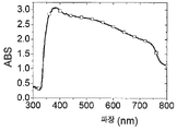
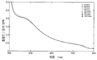
도 2(a)는 TiO2 위에 제조된 페로브스카이트 CH3NH3PbBr3의 UV-Vis 흡수 스펙트럼이다. 그래프 상에서 x축 상에 파장 (단위: nm)을 플롯하고, y축 상에 흡광도(임의 단위(arbitrary unit))를 플롯한다.
도 2(b)는 TiO2 위에 제조된 페로브스카이트 CH3NH3PbI3의 UV-Vis 흡수 스펙트럼이다. 그래프 상에서 x축 상에 파장 (단위: nm)을 플롯하고, y축 상에 흡광도(임의 단위)를 플롯한다.
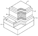
도 3은 일반적인 나노구조 태양 전지의 등각(isometric) 단면도이다: (1) 금속 캐소드, (2) 정공 전도성 물질(흡수체 및 정공 전도성 물질을 갖는 나노 구조 메조다공성 금속 산화물)(도 4에 더욱 명확하게 나타내었음) (3) 투명 전도성 금속 산화물(애노드), (4) 투명 기판, (5) 금속 애노드, (6) 조밀(compact) 금속 산화물.
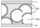
도 4는 일반적인 나노 구조 태양 전지의 '활성층'의 단면을 나타내는 개략도이다: (2(ⅰ)) 감광성 흡수체, (2(ⅱ)) 금속 산화물, 금속 캐소드, (6) 조밀 금속 산화물, (7) 정공 전도성 물질.
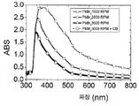
도 5는 유기금속 혼합 할라이드 층상 페로브스카이트의 UV-Vis 흡수 스펙트럼이다: 20 vol%로 TiO2 위에 제조된, K330 (CH3NH3PbCl2I) 및 K331 (CH3NH3PbCl2Br). 그래프 상에서 x축 상에 파장 (단위: nm)를 플롯하고, y축 상에 흡광도(임의 단위)를 플롯한다. 어두운 트레이스(trace)는 K330이고 밝은 트레이스는 K331이다.
도 6은 100 mWcm-2의 모사된 AM1.5G 조명 하에서 (상단 곡선) 그리고 암실에서 (하단 곡선)의, 이층 구조로 조립된 장치 (F:SnO2/조밀 TiO2/K330/스피로(spiro) OMeTAD/Ag)의 전류-전압 특성을 나타낸다. 그래프 상에서 x축 상에 전압(단위: V)을 플롯하고 y축 상에 전류 밀도 (단위: mAcm-2)를 플롯한다.
도 7은 모사된 AM1.5G 조명 하에서의, 정공 전도체를 갖는 흡수체 감응형(absorber-sensitised) 구조로 조립된 장치 (F:SnO2/조밀 TiO2/메조다공성 TiO2/K330/스피로 OMeTAD/Ag)의 전류-전압 특성을 나타낸다. 그래프 상에서 x축 상에 전압(단위: V)을 플롯하고 y축 상에 전류 밀도 (단위: mAcm-2)를 플롯한다.
도 8은 모사된 AM1.5G 조명 하에서의, 정공 전도체를 갖는 흡수체 감응형 구조로 조립된 장치(F:SnO2/조밀 TiO2/메조다공성 TiO2/K330/P3HT/Ag)의 전류-전압 특성을 나타낸다. 그래프 상에서 x축 상에 전압(단위: V)을 플롯하고 y축 상에 전류 밀도 (단위: mAcm-2)를 플롯한다.
도 9는 정공 전도체를 갖는 메조다공성 흡수체 구조로 조립된 장치(F:SnO2/조밀 TiO2/메조다공성 TiO2/K330/스피로 OMeTAD/Ag)의 입사 광자-전자 변환 효율(Incident Photon-to-Electron Conversion Efficiency; IPCE) 액션 스펙트럼을 나타낸다. 그래프 상에서 x축 상에 파장 (단위: nm)을 플롯하고 y축 상에 IPCE를 플롯한다.
도 10은 정공 전도체를 갖는 흡수체 감응형 구조로 조립된 장치 (F:SnO2/조밀 TiO2/메조다공성 TiO2/K330/P3HT (어두운 트레이스) 또는 PCPDTBT (밝은 트레이스)/Ag)의 입사 광자-전자 변환 효율(IPCE) 액션 스펙트럼을 나타낸다. 그래프 상에서 x축 상에 파장 (단위: nm)을 플롯하고 y축 상에 IPCE를 플롯한다.
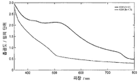
도 11은 썰린(surlyn) 및 에폭시를 사용하여 밀봉된 정공 전도체를 갖는 흡수체 감응형 구조로 조립된 장치 (F:SnO2/조밀 TiO2/메조다공성 산화물/K330/스피로 OMeTAD)의 UV-Vis 흡수 스펙트럼을 나타내며, 이때, 상기 스펙트럼은, 시간 경과에 따라 모사된 AM1.5G 조명 하에 광 조사하며(light soaking) 촬영한다, 그래프 상에서 x축 상에 파장 (단위: nm)를 플롯하고, y축 상에 흡광도(임의 단위)를 플롯한다.
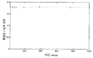
도 12는, 시간 경과에 따라, 모사된 AM1.5G 조명 하에 광 조사하며 500 nm에서 촬영한, 썰린 및 에폭시를 사용하여 밀봉된 정공 전도체를 갖는 흡수체 감응형 구조로 조립된 장치 (F:SnO2/조밀 TiO2/메조다공성 TiO2/K330/스피로 OMeTAD)의, UV-Vis 흡수 스펙트럼을 나타낸다. 그래프 상에서 x축 상에 시간(단위: hours)을 플롯하고, y축 상에 흡광도(임의의 단위)를 플롯한다.
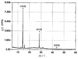
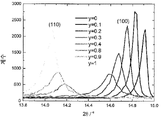
도 13은 유리 위에 35 vol%로 제조된 K330의 X-레이 회절(XRD) 스펙트럼을 나타낸다. x축 상에 2θ 각도를 플롯하고, y축 상에 계수(number of count)(임의 단위)를 플롯한다.
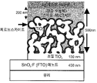
도 14는 메조다공성 TiO2의 단면의 주사전자현미경(SEM) 이미지를 나타낸다.
도 15는 메조다공성 TiO2/K330의 단면의 주사전자현미경(SEM) 이미지를 나타낸다.
도 16은 메조다공성 TiO2/K330/스피로 OMeTAD의 단면의 주사전자현미경(SEM) 이미지를 나타낸다.
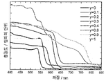
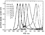
도 17(a)는 특정 범위의 FOPbI3yBr3(1-y) 페로브스카이트의 UV-vis 흡수 스펙트럼을 나타내고, 도 17(b)는 동일한 샘플의 정상 상태 광발광 스펙트럼을 나타낸다.
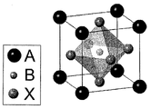
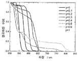
도 18(a-c)는 하기에 대한 개략도를 나타낸다: (a) 일반적인 페로브스카이트 ABX3의 단위 셀; (b) 입방정계 페로브스카이트 격자 구조(단위 셀은 중첩된 정사각형으로 나타냄); (c) BX6 팔면체의 뒤틀림에 기인하는 정방정계 페로브스카이트 격자 구조 (단위 셀은 더 큰 중첩된 정사각형으로 나타내고, 의사입방정계(pseudocubic) 단위 셀은, 그렇게 묘사될 수 있으면, 더 작은 중첩된 정사각형으로 나타냄).
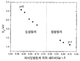
도 18(d)는 0 내지 1의 범위에 있는 다양한 값의 y에 대한 FOPbI3yBr3(1-y) 페로브스카이트의 X-레이 회절 데이터를 나타낸다. 도 18(e)는 시스템이 브롬 이온으로부터 요오드 이온으로 이동함에 따른, (100) 입방정계 피크 및 (110) 정방정계 피크 사이의 변이 과정의 확대도를 나타내는 데, 상기 변이 과정은 (100) 의사입방정계 피크에 상응한다. 도 18(f)는 계산된 의사입방정계 격자 파라미터에 대한 밴드 갭(band gap)의 플롯을 나타낸다.
도 19(a)는 정공 수송체로서 스피로-OMeTAD를 갖는 FOPbI3yBr3(1-y) 페로브스카이트 감광 메조다공성 티타니아를 포함하는 태양 전지의 회분의, 모사된 AM1.5 태양광 하에서 측정된, 평균 전류-전압 특성을 나타낸다. 도 19(b)는 대표 셀들의 정규화된 외부 양자 효율을 나타내고, 도 19(c)는 FOPbI3yBr3(1-y) 페로브스카이트에서, 요오드 분율 y의 함수로서의, 상기 회분에 대한 장치 성능 파라미터(device parameter of merit)의 플롯을 나타낸다.1 is a schematic diagram of a photoelectric conversion device including mixed anion perovskite.
FIG. 2(a) is a UV-Vis absorption spectrum of perovskite CH 3 NH 3 PbBr 3 prepared on TiO 2 . On the graph, the wavelength (unit: nm) is plotted on the x-axis, and the absorbance (arbitrary unit) is plotted on the y-axis.
FIG. 2(b) is a UV-Vis absorption spectrum of perovskite CH 3 NH 3 PbI 3 prepared on TiO 2 . On the graph, the wavelength (unit: nm) is plotted on the x-axis, and the absorbance (arbitrary unit) is plotted on the y-axis.
3 is an isometric cross-sectional view of a typical nanostructured solar cell: (1) a metal cathode, (2) a hole conducting material (a nanostructured mesoporous metal oxide with an absorber and a hole conducting material) (more clearly shown in FIG. 4 ) shown) (3) transparent conductive metal oxide (anode), (4) transparent substrate, (5) metal anode, (6) compact metal oxide.
4 is a schematic diagram showing a cross-section of an 'active layer' of a typical nanostructured solar cell: (2(i)) a photosensitive absorber, (2(ii)) a metal oxide, a metal cathode, (6) a dense metal oxide, (7) hole-conducting material.
5 is a UV-Vis absorption spectrum of an organometallic mixed halide layered perovskite: K330 (CH 3 NH 3 PbCl 2 I) and K331 (CH 3 NH 3 PbCl 2 Br, prepared on TiO 2 at 20 vol%). ). On the graph, the wavelength (unit: nm) is plotted on the x-axis, and the absorbance (arbitrary unit) is plotted on the y-axis. The dark trace is K330 and the light trace is K331.
6 is 100 mWcm -2 of simulated Current-voltage characteristics of the bilayered device (F:SnO 2 /Dense TiO 2 /K330/spiro OMeTAD/Ag) under AM1.5G illumination (top curve) and in the dark (bottom curve). indicates. On the graph, the voltage (unit: V) is plotted on the x-axis and the current density (unit: mAcm -2 ) is plotted on the y-axis.
7 is a simulated Current-Voltage Characteristics of Devices (F:SnO 2 /Dense TiO 2 /Mesoporous TiO 2 /K330/spiro OMeTAD/Ag) fabricated into an absorber-sensitised structure with hole conductors under AM1.5G illumination indicates On the graph, the voltage (unit: V) is plotted on the x-axis and the current density (unit: mAcm -2 ) is plotted on the y-axis.
8 is a simulated Current-voltage characteristics of a device (F:SnO 2 /dense TiO 2 /mesoporous TiO 2 /K330/P3HT/Ag) assembled into an absorber-sensitive structure with hole conductors under AM1.5G illumination. On the graph, the voltage (unit: V) is plotted on the x-axis and the current density (unit: mAcm -2 ) is plotted on the y-axis.
9 is an incident photon-to-electron conversion efficiency of a device (F:SnO 2 /dense TiO 2 /mesoporous TiO 2 /K330/spiro OMeTAD/Ag) assembled into a mesoporous absorber structure with hole conductors. Electron Conversion Efficiency (IPCE) represents the action spectrum. On the graph, the wavelength (unit: nm) is plotted on the x-axis and the IPCE is plotted on the y-axis.
Figure 10 shows incident photons of a device assembled into an absorber-sensitive structure with hole conductors (F:SnO 2 /Dense TiO 2 /Mesoporous TiO 2 /K330/P3HT (dark trace) or PCPDTBT (light trace)/Ag)- It represents the electron conversion efficiency (IPCE) action spectrum. On the graph, the wavelength (unit: nm) is plotted on the x-axis and the IPCE is plotted on the y-axis.
FIG. 11 shows UV-Vis absorption of a device (F:SnO 2 /Dense TiO 2 /Mesoporous oxide/K330/spiro OMeTAD) assembled into an absorber-sensitive structure with hole conductors sealed using surlyn and epoxy. represents a spectrum, wherein the spectrum is simulated over time Light soaking is performed under AM1.5G illumination, and on the graph, the wavelength (unit: nm) is plotted on the x-axis, and the absorbance (arbitrary unit) is plotted on the y-axis.
12, over time, simulated Devices assembled into absorber-sensitive structures with hole conductors sealed using slicing and epoxy, photographed at 500 nm under AM1.5G illumination (F:SnO 2 /Dense TiO 2 /Mesoporous TiO 2 /K330) /spiro shows the UV-Vis absorption spectrum of OMeTAD). On the graph, time (unit: hours) is plotted on the x-axis, and absorbance (arbitrary unit) is plotted on the y-axis.
13 shows an X-ray diffraction (XRD) spectrum of K330 prepared at 35 vol% on glass. Plot the 2θ angles on the x-axis, and the number of counts (in arbitrary units) on the y-axis.
14 shows a scanning electron microscope (SEM) image of a cross-section of mesoporous TiO 2 .
15 shows a scanning electron microscope (SEM) image of a cross-section of mesoporous TiO 2 /K330.
16 shows a scanning electron microscope (SEM) image of a cross-section of mesoporous TiO 2 /K330/spiro OMeTAD.
Fig. 17(a) shows the UV-vis absorption spectrum of a specific range of FOPbI 3y Br 3(1-y) perovskite, and Fig. 17(b) shows the steady-state photoluminescence spectrum of the same sample.
Figure 18(ac) shows a schematic diagram for: (a) a unit cell of a typical perovskite ABX 3 ; (b) cubic perovskite lattice structure (unit cells are represented by superimposed squares); (c) tetragonal perovskite lattice structure due to distortion of the BX 6 octahedron (unit cells are represented by larger overlapping squares and pseudocubic unit cells, if so delineated, with smaller overlap represented by a square).
Fig. 18(d) shows X-ray diffraction data of FOPbI 3y Br 3(1-y) perovskite for various values of y in the range of 0 to 1. Figure 18(e) shows an enlarged view of the transition process between the (100) cubic peak and the (110) tetragonal peak as the system moves from the bromine ion to the iodine ion, the transition process being the (100) pseudo It corresponds to the cubic peak. Fig. 18(f) shows a plot of the band gap versus the calculated pseudocubic lattice parameters.
Figure 19(a) is a measurement under simulated AM1.5 sunlight of a batch of solar cells containing FOPbI 3y Br 3(1-y) perovskite photosensitive mesoporous titania with spiro-OMeTAD as hole transporter. and average current-voltage characteristics. Fig. 19(b) shows the normalized external quantum efficiencies of representative cells, and Fig. 19(c) shows the apparatus for the batch as a function of iodine fraction y, in FOPbI 3y Br 3(1-y) perovskite. A plot of the device parameter of merit is shown.
본 발명은 혼합 음이온 페로브스카이트(mixed-anion perovskite)를 포함하는 광전자 장치를 제공하며, 여기서 상기 혼합 음이온 페로브스카이트는 할라이드 음이온 및 칼코게나이드 음이온으로부터 선택된 2종 이상의 서로 상이한 음이온을 포함한다.The present invention provides an optoelectronic device comprising a mixed-anion perovskite, wherein the mixed-anion perovskite comprises at least two different anions selected from a halide anion and a chalcogenide anion. .
광전자 장치는 광 에너지를 전기 에너지로 전환하거나 전기 에너지를 광 에너지로 전환할 수 있는 모든 장치이다.An optoelectronic device is any device capable of converting light energy into electrical energy or converting electrical energy into light energy.
본 명세서에서 사용되는, 용어 "페로브스카이트"는 CaTiO3의 결정 구조와 관련된 3차원 결정 구조를 갖는 물질을 지칭하거나, 물질의 층을 포함하는 물질을 지칭하는 데, 여기서 상기 층은 CaTiO3의 구조와 관련된 구조를 갖는다. CaTiO3의 구조는 화학식 ABX3로 표시될 수 있으며, 상기 화학식 중 A 및 B는 서로 상이한 크기의 양이온이고 X는 음이온이다. 단위 셀에서, A 양이온은 (0,0,0)에 위치하고, B 양이온은 (1/2,1/2,1/2)에 위치하고 X 음이온은 (1/2,1/2,0)에 위치한다. A 양이온은 통상적으로 B 양이온보다 크다. 통상의 기술자는 A, B 및 X가 달라지는 경우, 상이한 이온 크기가 페로브스카이트 재료의 구조를 CaTiO3에 의해 채택된 구조로부터 낮은 대칭성을 갖는 뒤틀린 구조로 뒤틀려져 버리게 할 수 있다는 것을 이해할 것이다. 또한, 상기 대칭성은 상기 재료가 CaTiO3의 구조와 관련된 구조를 갖는 층을 포함하는 경우 저하될 것이다. 페로브스카이트 재료의 층을 포함하는 재료는 잘 알려져 있다. 예를 들어, K2NiF4 형 구조를 채용하는 재료의 구조는 페로브스카이트 재료의 층을 포함한다. 또한, 통상의 기술자는 페로브스카이트 재료는 화학식 [A][B][X]3로 표시될 수 있고, 상기 화학식 중 A는 적어도 1종의 양이온이고, B는 적어도 1종의 양이온이고, X는 적어도 1종의 음이온이라는 것을 이해할 것이다. 상기 페로브스카이트가 2종 이상의 A 양이온을 포함하는 경우, 상이한 A 양이온은 규칙적 또는 불규칙적으로 A 사이트에 분배될 수 있다. 상기 페로브스카이트가 2종 이상의 B 양이온을 포함하는 경우, 상이한 B 양이온은 규칙적 또는 불규칙적으로 B 사이트에 분배될 수 있다. 상기 페로브스카이트가 2종 이상의 X 음이온을 포함하는 경우, 상이한 X 음이온은 규칙적 또는 불규칙적으로 X 사이트에 분배될 수 있다. 2종 이상의 A 양이온, 2종 이상의 B 양이온 또는 2종 이상의 X 양이온을 포함하는 페로브스카이트의 대칭성은 CaTiO3의 대칭성보다 낮을 것이다.As used herein, the term “perovskite” refers to a material having a three-dimensional crystal structure related to the crystal structure of CaTiO 3 , or refers to a material comprising a layer of material, wherein the layer is CaTiO 3 has a structure related to the structure of The structure of CaTiO 3 may be represented by Chemical Formula ABX 3 , wherein A and B are cations having different sizes, and X is an anion. In the unit cell, the A cation is located at (0,0,0), the B cation is located at (1/2,1/2,1/2) and the X anion is located at (1/2,1/2,0). Located. The A cation is usually larger than the B cation. A person skilled in the art will understand that, when A, B and X are different, different ion sizes can cause the structure of the perovskite material to warp from the structure adopted by CaTiO 3 to the warped structure with low symmetry. Also, the symmetry will be degraded if the material comprises a layer having a structure related to that of CaTiO 3 . Materials comprising a layer of perovskite material are well known. For example, a structure of a material employing a K 2 NiF 4 type structure comprises a layer of perovskite material. In addition, those skilled in the art will know that the perovskite material may be represented by the formula [A][B][X] 3 , wherein A is at least one cation, B is at least one cation, It will be understood that X is at least one anion. When the perovskite includes two or more kinds of A cations, different A cations may be regularly or irregularly distributed to the A sites. When the perovskite contains two or more kinds of B cations, different B cations may be distributed to the B sites regularly or irregularly. When the perovskite contains two or more kinds of X anions, different X anions may be regularly or irregularly distributed to the X sites. The symmetry of a perovskite comprising two or more A cations, two or more B cations or two or more X cations will be lower than that of CaTiO 3 .
본 명세서에서 사용되는, 용어 "혼합 음이온"은 적어도 2종의 서로 상이한 음이온을 포함하는 화합물을 지칭한다.As used herein, the term "mixed anion" refers to a compound comprising at least two mutually different anions.
용어 "할라이드"는 7족 원소, 즉 할로겐의 음이온을 지칭한다. 전형적으로, 할라이드는 불소 음이온, 염소 음이온, 브롬 음이온, 요오드 음이온 또는 아스타틴 음이온을 지칭한다.The term “halide” refers to an anion of a
본 명세서에서 사용되는, "칼코게나이드 음이온"은 6족 원소, 즉 칼코겐의 음이온을 지칭한다. 전형적으로, 칼코게나이드는 산소 음이온, 황 음이온, 셀레늄 음이온 또는 텔루륨 음이온을 지칭한다.As used herein, "chalcogenide anion" refers to an anion of a
본 발명의 광전자 장치에서 혼합 음이온 페로브스카이트는 제1 양이온, 제2 양이온 및 상기 2종 이상의 서로 상이한 음이온을 포함할 수 있다.In the optoelectronic device of the present invention, the mixed anion perovskite may include a first cation, a second cation, and two or more different anions from each other.
통상의 기술자가 이해할 수 있는 바와 같이, 혼합 음이온 페로브스카이트는 추가적인 양이온 또는 추가적인 음이온을 포함할 수 있다. 예를 들어, 혼합 음이온 페로브스카이트는 2종, 3종 또는 4종의 서로 상이한 양이온, 또는 2종, 3종 또는 4종의 서로 상이한 음이온을 포함할 수 있다.As will be appreciated by those of ordinary skill in the art, the mixed anion perovskite may include additional cations or additional anions. For example, a mixed anion perovskite may comprise two, three or four different cations, or two, three or four different anions.
일 구현예에서, 페로브스카이트는 할라이드 음이온 및 칼코게나이드 음이온으로부터 선택된 2종의 서로 상이한 음이온을 포함한다. 2종의 서로 상이한 음이온은 할라이드 음이온 및 칼코게나이드 음이온이거나, 2종의 서로 상이한 할라이드 음이온이거나, 또는 2종의 서로 상이한 칼코게나이드 음이온일 수 있다.In one embodiment, the perovskite comprises two different anions selected from a halide anion and a chalcogenide anion. The two different anions may be halide anions and chalcogenide anions, two different halide anions, or two different chalcogenide anions.
전형적으로, 본 발명의 광전자 장치에서, 혼합 음이온 페로브스카이트 중의 제2 양이온은 금속 양이온이다. 더욱 전형적으로, 제2 양이온은 2가 금속 양이온이다. 예를 들어, 제2 양이온은 Ca2+, Sr2+, Cd2+, Cu2+, Ni2+, Mn2+, Fe2+, Co2+, Pd2+, Ge2+, Sn2+, Pb2+, Sn2+, Yb2+ 및 Eu2+으로부터 선택될 수 있다. 통상적으로, 제2 양이온은 Sn2+ 및 Pb2+로부터 선택된다.Typically, in the optoelectronic device of the present invention, the second cation in the mixed anion perovskite is a metal cation. More typically, the second cation is a divalent metal cation. For example, the second cation can be Ca 2+ , Sr 2+ , Cd 2+ , Cu 2+ , Ni 2+ , Mn 2+ , Fe 2+ , Co 2+ , Pd 2+ , Ge 2+ , Sn 2 + , Pb 2+ , Sn 2+ , Yb 2+ and Eu 2+ . Typically, the second cation is selected from Sn 2+ and Pb 2+ .
본 발명의 광전자 장치에서, 혼합 음이온 페로브스카이트 중의 제1 양이온은 통상적으로 유기 양이온이다.In the optoelectronic device of the present invention, the first cation in the mixed anion perovskite is typically an organic cation.
용어 "유기 양이온"은 탄소를 포함하는 양이온을 지칭한다. 유기 양이온은 추가적인 원소를 포함할 수 있고, 예를 들어, 유기 양이온은 수소, 질소 또는 산소를 포함할 수 있다.The term “organic cation” refers to a cation comprising carbon. The organic cation may include additional elements, for example, the organic cation may include hydrogen, nitrogen or oxygen.
페로브스카이트 중의 유기 양이온(또는 유기 양이온들)의 변경은 통상적으로 페로브스카이트의 구조적 및/또는 물리적 특성에 영향을 미칠 것이다. 사용되는 유기 양이온을 제어함으로써, 재료의 전자 특성 및 광학 특성은 제어될 수 있다. 페로브스카이트에 의해 표시되는 특성에 대한 이러한 유연한 제어는 상기 페로브스카이트를 포함하는 광전자 장치의 특성을 조절하는 데 특히 유용하다. 예를 들어, 유기 양이온을 변경함으로써, 재료의 전도도가 증가하거나 감소할 수 있다. 또한, 유기 양이온의 변경은 재료의 밴드 구조를 변경할 수 있고 이에 따라, 예를 들어, 반도체성 재료의 밴드 갭을 제어할 수 있다.Alteration of the organic cation (or organic cations) in the perovskite will typically affect the structural and/or physical properties of the perovskite. By controlling the organic cations used, the electronic and optical properties of the material can be controlled. This flexible control over the properties displayed by the perovskite is particularly useful for tuning the properties of optoelectronic devices comprising the perovskite. For example, by altering the organic cations, the conductivity of the material can be increased or decreased. Also, altering the organic cations can alter the band structure of the material and thus control the band gap of, for example, semiconducting materials.
통상적으로, 본 발명의 광전자 장치에서, 유기 양이온은 화학식 (R1R2R3R4N)+을 가지며, 여기서, R1은 수소, 비치환 또는 치환된 C1-C20 알킬 또는 비치환 또는 치환된 아릴이고; R2는 수소, 비치환 또는 치환된 C1-C20 알킬 또는 비치환 또는 치환된 아릴이고; R3는 수소, 비치환 또는 치환된 C1-C20 알킬 또는 비치환 또는 치환된 아릴이고; R4는 수소, 비치환 또는 치환된 C1-C20 알킬 또는 비치환 또는 치환된 아릴이다.Typically, in the optoelectronic device of the present invention, the organic cation has the formula (R 1 R 2 R 3 R 4 N) + , wherein R 1 is hydrogen, unsubstituted or substituted C 1 -C 20 alkyl or unsubstituted or substituted aryl; R 2 is hydrogen, unsubstituted or substituted C 1 -C 20 alkyl or unsubstituted or substituted aryl; R 3 is hydrogen, unsubstituted or substituted C 1 -C 20 alkyl or unsubstituted or substituted aryl; R 4 is hydrogen, unsubstituted or substituted C 1 -C 20 alkyl or unsubstituted or substituted aryl.
본 명세서에서 사용되는 바와 같이, 알킬기는 치환 또는 비치환된, 직쇄 또는 분지쇄 포화 라디칼일 수 있고, 알킬기는 종종 치환 또는 비치환된 직쇄 포화 라디칼이고, 더욱 종종 비치환된 직쇄 포화 라디칼이다. C1-C20 알킬기는 1 내지 20개의 탄소 원자를 갖는, 비치환 또는 치환된, 직쇄 또는 분지쇄 포화 탄화수소 라디칼이다. 이는, 전형적으로, C1-C10 알킬이고, 구체적인 예를 들면, 메틸기, 에틸, 프로필, 부틸, 펜틸, 헥실, 헵틸, 옥틸, 노닐 또는 데실이고, 또는, 이는 C1-C6 알킬이고, 예를 들어, 메틸, 에틸, 프로필, 부틸, 펜틸 또는 헥실이고, 또는, 이는 C1-C4 알킬이고, 예를 들어, 메틸, 에틸, i-프로필, n-프로필, t-부틸, s-부틸 또는 n-부틸이다.As used herein, an alkyl group can be a substituted or unsubstituted, straight-chain or branched saturated radical, an alkyl group is often a substituted or unsubstituted straight-chain saturated radical, and more often an unsubstituted straight-chain saturated radical. A C 1 -C 20 alkyl group is an unsubstituted or substituted, straight or branched chain saturated hydrocarbon radical having 1 to 20 carbon atoms. It is typically C 1 -C 10 alkyl, for example a methyl group, ethyl, propyl, butyl, pentyl, hexyl, heptyl, octyl, nonyl or decyl, or it is C 1 -C 6 alkyl, for example methyl, ethyl, propyl, butyl, pentyl or hexyl, or it is C 1 -C 4 alkyl, for example methyl, ethyl, i-propyl, n-propyl, t-butyl, s- butyl or n-butyl.
알킬기가 치환되는 경우, 알킬기는 전형적으로 치환 또는 비치환된 C1-C20 알킬, 치환 또는 비치환된 아릴 (본 명세서에서 정의된 바와 같음), 시아노, 아미노, C1-C10 알킬아미노, 디(C1-C10)알킬아미노, 아릴아미노, 디아릴아미노, 아릴알킬아미노, 아미도, 아실아미도, 히드록시, 옥소, 할로, 카르복시, 에스테르, 아실, 아실옥시, C1-C20 알콕시, 아릴옥시, 할로알킬, 술폰산, 술프히드릴(즉, 티올, -SH), C1-C10 알킬티오, 아릴티오, 술포닐, 인산, 포스페이트 에스테르, 포스폰산 및 포스포네이트 에스테르로부터 선택된 하나 이상의 치환기를 갖는다. 치환된 알킬기의 예에는, 할로알킬, 히드록시알킬, 아미노알킬, 알콕시알킬 및 알크아릴기가 포함된다. 본 명세서에서 사용되는, 용어 알크아릴은 적어도 하나의 수소 원자가 아릴기로 치환되는 C1-C20 알킬기에 관한 것이다. 이러한 기들의 예는 벤질 (페닐메틸, PhCH2-), 벤즈히드릴 (Ph2CH-), 트리틸 (트리페닐메틸, Ph3C-), 페네틸 (페닐에틸, Ph-CH2CH2-), 스티릴 (Ph-CH=CH-), 신나밀 (Ph-CH=CH-CH2-)을 포함하지만, 이에 제한되지 않는다.When an alkyl group is substituted, the alkyl group is typically substituted or unsubstituted C 1 -C 20 alkyl, substituted or unsubstituted aryl (as defined herein), cyano, amino, C 1 -C 10 alkylamino. , di(C 1 -C 10 )alkylamino, arylamino, diarylamino, arylalkylamino, amido, acylamido, hydroxy, oxo, halo, carboxy, ester, acyl, acyloxy, C 1 -C 20 from alkoxy, aryloxy, haloalkyl, sulfonic acid, sulfhydryl (ie thiol, -SH), C 1 -C 10 alkylthio, arylthio, sulfonyl, phosphoric acid, phosphate ester, phosphonic acid and phosphonate ester has one or more selected substituents. Examples of the substituted alkyl group include haloalkyl, hydroxyalkyl, aminoalkyl, alkoxyalkyl and alkaryl groups. As used herein, the term alkaryl relates to a C 1 -C 20 alkyl group in which at least one hydrogen atom is replaced by an aryl group. Examples of such groups are benzyl (phenylmethyl, PhCH 2 -), benzhydryl (Ph 2 CH-), trityl (triphenylmethyl, Ph 3 C-), phenethyl (phenylethyl, Ph-CH 2 CH 2 ) -), styryl (Ph-CH=CH-), cinnamyl (Ph-CH=CH-CH 2 -).
전형적으로 치환된 알킬기는 1, 2 또는 3개, 예를 들어, 1 또는 2개의 치환기를 수반한다.Typically substituted alkyl groups carry 1, 2 or 3, eg, 1 or 2, substituents.
아릴기는 치환 또는 비치환된, 모노사이클릭 또는 바이사이클릭 방향족 기이며, 이는 전형적으로 고리 부분에서, 6 내지 14개의 탄소 원자, 바람직하게는 6 내지 10개의 탄소 원자를 포함한다. 아릴기의 예들은 페닐, 나프틸, 인데닐 및 인다닐기를 포함한다. 아릴기는 비치환 또는 치환된다. 상술한 바와 같은 아릴기가 치환되는 경우, 아릴기는 전형적으로 (아랄킬기를 형성하는) 비치환된 C1-C6 알킬기, 비치환된 아릴, 시아노, 아미노, C1-C10 알킬아미노, 디(C1-C10)알킬아미노, 아릴아미노, 디아릴아미노, 아릴알킬아미노, 아미도, 아실아미도, 히드록시, 할로, 카르복시, 에스테르, 아실, 아실옥시, C1-C20 알콕시, 아릴옥시, 할로알킬, 술프히드릴(즉, 티올, -SH), C1-C10 알킬티오, 아릴티오, 술폰산, 인산, 포스페이트 에스테르, 포스폰산과 포스포네이트 에스테르 및 술포닐로부터 선택되는 하나 이상의 치환기를 갖는다. 전형적으로, 아릴기는 0, 1, 2 또는 3개의 치환기를 수반한다. 치환된 아릴기는 1좌(single) C1-C6 알킬렌기로, 또는 화학식 -X-(C1-C6)알킬렌, 또는 -X-(C1-C6)알킬렌-X- (여기서, X는 O, S 및 NR (여기서 R은 H, 아릴 또는 C1-C6 알킬이다)로부터 선택된다)로 표시되는 2좌(bidentate) 기로 2개의 위치에서 치환될 수 있다. 따라서 치환된 아릴기는 시클로알킬기 또는 헤테로시클일기와 융합된 아릴기일 수 있다. 아릴기의 고리 원자는 (헤테로아릴기와 같이) 하나 이상의 헤테로원자를 포함할 수 있다. 이러한 아릴기 (헤테로아릴기)는 치환 또는 비치환된 모노- 또는 바이사이클릭 헤테로방향족 기인 데, 이는 전형적으로 하나 이상의 헤테로원자를 포함하는 고리 부분에 6 내지 10개의 원자를 포함한다. 이는, 일반적으로 5원 또는 6원 고리이고, O, S, N, P, Se 및 Si로부터 선택된 하나 이상의 헤테로 원자를 포함한다. 이는 예를 들어, 1, 2 또는 3개의 헤테로원자를 포함할 수 있다. 헤테로아릴기의 예들은 티오페닐, 피리딜, 피라지닐, 피리미디닐, 피리다지닐, 퓨라닐, 티에닐, 피라졸리디닐, 피롤일, 옥사졸일, 옥사디아졸일, 이속사졸릴, 티아디아졸일, 티아졸일, 이소티아졸일, 이미다졸일, 피라졸일, 퀴놀일 및 이소퀴놀일을 포함한다. 헤테로아릴기는 예를 들어, 아릴에 대해 명시된 바와 같이, 비치환 또는 치환될 수 있다. 전형적으로, 헤테로아릴기는 0, 1, 2 또는 3개의 치환기를 수반한다.An aryl group is a substituted or unsubstituted, monocyclic or bicyclic aromatic group, which typically contains in the
주로, 본 발명의 광전자 장치에서, 유기 양이온에서의 R1은 수소, 메틸 또는 에틸이고, R2은 수소, 메틸 또는 에틸이고, R3은 수소, 메틸 또는 에틸이고, R4은 수소, 메틸 또는 에틸이다. 예를 들어, R1은 수소 또는 메틸일 수 있고, R2은 수소 또는 메틸일 수 있고, R3은 수소 또는 메틸일 수 있고, R4은 수소 또는 메틸일 수 있다.Mainly, in the optoelectronic device of the present invention, R 1 in the organic cation is hydrogen, methyl or ethyl, R 2 is hydrogen, methyl or ethyl, R 3 is hydrogen, methyl or ethyl, R 4 is hydrogen, methyl or is ethyl. For example, R 1 can be hydrogen or methyl, R 2 can be hydrogen or methyl, R 3 can be hydrogen or methyl, and R 4 can be hydrogen or methyl.
대안적으로, 유기 양이온은 화학식 (R5NH3)+을 가질 수 있고, 여기서, R5는 수소, 또는 비치환 또는 치환된 C1-C20 알킬이다. 예를 들어, R5는 메틸 또는 에틸일 수 있다. 전형적으로, R5는 메틸이다.Alternatively, the organic cation may have the formula (R 5 NH 3 ) + , wherein R 5 is hydrogen or unsubstituted or substituted C 1 -C 20 alkyl. For example, R 5 can be methyl or ethyl. Typically, R 5 is methyl.
일부 구현예에서, 유기 양이온은 화학식 (R5R6N=CH-NR7R8)+을 가지고, 여기서In some embodiments, the organic cation has the formula (R 5 R 6 N=CH-NR 7 R 8 ) + , wherein
R5는 수소, 비치환 또는 치환된 C1-C20 알킬, 또는 비치환 또는 치환된 아릴이고;R 5 is hydrogen, unsubstituted or substituted C 1 -C 20 alkyl, or unsubstituted or substituted aryl;
R6는 수소, 비치환 또는 치환된 C1-C20 알킬, 또는 비치환 또는 치환된 아릴이고;R 6 is hydrogen, unsubstituted or substituted C 1 -C 20 alkyl, or unsubstituted or substituted aryl;
R7는 수소, 비치환 또는 치환된 C1-C20 알킬, 또는 비치환 또는 치환된 아릴이고;R 7 is hydrogen, unsubstituted or substituted C 1 -C 20 alkyl, or unsubstituted or substituted aryl;
R8는 수소, 비치환 또는 치환된 C1-C20 알킬, 또는 비치환 또는 치환된 아릴이다.R 8 is hydrogen, unsubstituted or substituted C 1 -C 20 alkyl, or unsubstituted or substituted aryl.
전형적으로, 유기 양이온에서의 R5는 수소, 메틸 또는 에틸이고, R6은 수소, 메틸 또는 에틸이고, R7은 수소, 메틸 또는 에틸이고, R8은 수소, 메틸 또는 에틸이다. 예를 들어, R5은 수소 또는 메틸일 수 있고, R6은 수소 또는 메틸일 수 있고, R7은 수소 또는 메틸일 수 있고, R8은 수소 또는 메틸일 수 있다.Typically, in an organic cation, R 5 is hydrogen, methyl or ethyl, R 6 is hydrogen, methyl or ethyl, R 7 is hydrogen, methyl or ethyl, and R 8 is hydrogen, methyl or ethyl. For example, R 5 can be hydrogen or methyl, R 6 can be hydrogen or methyl, R 7 can be hydrogen or methyl, and R 8 can be hydrogen or methyl.
유기 양이온은 예를 들어, 화학식 (H2N=CH-NH2)+을 가질 수 있다.The organic cation can have, for example, the formula (H 2 N=CH—NH 2 ) + .
본 발명의 광전자 장치에서, 페로브스카이트는 통상적으로 혼합 할라이드 페로브스카이트이며, 여기서 상기 2종 이상의 서로 상이한 음이온은 2종 이상의 서로 상이한 할라이드 음이온이다. 전형적으로, 이들은 2종 또는 3종의 할라이드 음이온이고, 더욱 전형적으로, 2종의 서로 상이한 할라이드 음이온이다. 통상적으로 할라이드 음이온은 불소 이온, 염소 이온, 브롬 이온 및 요오드 이온으로부터 선택되고, 예를 들어 염소 이온, 브롬 이온 및 요오드 이온으로부터 선택된다.In the optoelectronic device of the present invention, the perovskite is typically a mixed halide perovskite, wherein the at least two different anions are two or more different halide anions. Typically, these are two or three halide anions, more typically two different halide anions. Typically, the halide anion is selected from a fluorine ion, a chlorine ion, a bromine ion and an iodine ion, for example a chlorine ion, a bromine ion and an iodine ion.
전형적으로, 본 발명의 광전자 장치에서, 페로브스카이트는 하기 화학식 (Ⅰ)의 페로브스카이트 화합물이다:Typically, in the optoelectronic device of the present invention, the perovskite is a perovskite compound of formula (I):
[A][B][X]3 (Ⅰ)[A][B][X] 3 (Ⅰ)
상기 화학식 (Ⅰ) 중,In the above formula (I),
[A]는 적어도 1종의 유기 양이온이고;[A] is at least one organic cation;
[B]는 적어도 1종의 금속 양이온이고;[B] is at least one metal cation;
[X]는 상기 2종 이상의 서로 상이한 음이온이다.[X] is the above-mentioned two or more kinds of mutually different anions.
예를 들어, 상기 화학식 (Ⅰ)의 페로브스카이트는 1종의 금속 양이온을 포함하거나, 2종, 3종 또는 4종의 서로 상이한 금속 양이온을 포함할 수 있고, 전형적으로, 1종의 금속 양이온을 포함하거나, 2종의 서로 상이한 금속 양이온을 포함할 수 있다. 상기 화학식 (Ⅰ)의 페로브스카이트는 예를 들어, 1종의 유기 양이온을 포함하거나, 2종, 3종 또는 4종의 서로 상이한 유기 양이온을 포함할 수 있고, 전형적으로, 1종의 유기 양이온을 포함하거나, 2종의 서로 상이한 유기 양이온을 포함할 수 있다. 상기 화학식 (Ⅰ)의 페로브스카이트는 예를 들어, 2종, 3종 또는 4종의 서로 상이한 음이온을 포함할 수 있고, 전형적으로, 2종 또는 3종의 서로 상이한 음이온을 포함할 수 있다.For example, the perovskite of formula (I) may comprise one metal cation, or may comprise two, three or four different metal cations, typically one metal cation. or may include two different metal cations. The perovskite of formula (I) may comprise, for example, one organic cation or may comprise two, three or four different organic cations, typically one organic cation. or may include two different organic cations. The perovskite of formula (I) may comprise, for example, two, three or four different anions, and typically, two or three different anions.
종종, 본 발명의 광전자 장치에서, [X]는 할라이드 음이온 및 칼코게나이드 음이온, 2종의 서로 상이한 할라이드 음이온 또는 2종의 서로 상이한 칼코게나이드 음이온이다.Often, in the optoelectronic device of the present invention, [X] is a halide anion and a chalcogenide anion, two different halide anions or two different chalcogenide anions.
전형적으로, 본 발명의 광전자 장치에서, 혼합 음이온 페로브스카이트 중의 [B]는 적어도 1종의 금속 양이온이다. 더욱 전형적으로, [B]는 적어도 1종의 2가 금속 양이온이다. 예를 들어, [B]는 Ca2+, Sr2+, Cd2+, Cu2+, Ni2+, Mn2+, Fe2+, Co2+, Pd2+, Ge2+, Sn2+, Pb2+, Sn2+, Yb2+ 및 Eu2+로부터 선택될 수 있는 적어도 1종의 2가 금속 양이온이다. 통상적으로, [B]는 Sn2+ 및 Pb2+로부터 선택된 적어도 1종의 2가 금속 양이온이다.Typically, in the optoelectronic device of the present invention, [B] in the mixed anion perovskite is at least one metal cation. More typically, [B] is at least one divalent metal cation. For example, [B] is Ca 2+ , Sr 2+ , Cd 2+ , Cu 2+ , Ni 2+ , Mn 2+ , Fe 2+ , Co 2+ , Pd 2+ , Ge 2+ , Sn 2 at least one divalent metal cation that may be selected from + , Pb 2+ , Sn 2+ , Yb 2+ and Eu 2+ . Typically, [B] is at least one divalent metal cation selected from Sn 2+ and Pb 2+ .
통상적으로, 본 발명의 광전자 장치에서, [A]는 화학식 (R1R2R3R4N)+을 갖는 적어도 1종의 유기 양이온이며, 여기서 Typically, in the optoelectronic device of the present invention, [A] is at least one organic cation having the formula (R 1 R 2 R 3 R 4 N) + , wherein
R1은 수소, 비치환 또는 치환된 C1-C20 알킬 또는 비치환 또는 치환된 아릴이고;R 1 is hydrogen, unsubstituted or substituted C 1 -C 20 alkyl or unsubstituted or substituted aryl;
R2는 수소, 비치환 또는 치환된 C1-C20 알킬 또는 비치환 또는 치환된 아릴이고;R 2 is hydrogen, unsubstituted or substituted C 1 -C 20 alkyl or unsubstituted or substituted aryl;
R3는 수소, 비치환 또는 치환된 C1-C20 알킬 또는 비치환 또는 치환된 아릴이고;R 3 is hydrogen, unsubstituted or substituted C 1 -C 20 alkyl or unsubstituted or substituted aryl;
R4는 수소, 비치환 또는 치환된 C1-C20 알킬 또는 비치환 또는 치환된 아릴이다.R 4 is hydrogen, unsubstituted or substituted C 1 -C 20 alkyl or unsubstituted or substituted aryl.
그러나, [A]는 화학식 (R5R6N=CH-NR7R8)+을 갖는 적어도 1종의 유기 양이온일 수 있으며, 여기서, R5은 수소, 비치환 또는 치환된 C1-C20 알킬 또는 비치환 또는 치환된 아릴이고; R6는 수소, 비치환 또는 치환된 C1-C20 알킬 또는 비치환 또는 치환된 아릴이고; R7는 수소, 비치환 또는 치환된 C1-C20 알킬 또는 비치환 또는 치환된 아릴이고; R8는 수소, 비치환 또는 치환된 C1-C20 알킬 또는 비치환 또는 치환된 아릴이다.However, [A] can be at least one organic cation having the formula (R 5 R 6 N=CH-NR 7 R 8 ) + , wherein R 5 is hydrogen, unsubstituted or substituted C 1 -C 20 alkyl or unsubstituted or substituted aryl; R 6 is hydrogen, unsubstituted or substituted C 1 -C 20 alkyl or unsubstituted or substituted aryl; R 7 is hydrogen, unsubstituted or substituted C 1 -C 20 alkyl or unsubstituted or substituted aryl; R 8 is hydrogen, unsubstituted or substituted C 1 -C 20 alkyl or unsubstituted or substituted aryl.
일 구현예에서, 상기 페로브스카이트는 하기 화학식 (ⅠA)의 페로브스카이트 화합물이다:In one embodiment, the perovskite is a perovskite compound of formula (IA):
AB[X]3 (ⅠA)AB[X] 3 (IA)
상기 화학식 (ⅠA) 중,In the above formula (IA),
A는 유기 양이온이고;A is an organic cation;
B는 금속 양이온이고;B is a metal cation;
[X]는 상기 2종 이상의 서로 상이한 음이온이다.[X] is the above-mentioned two or more kinds of mutually different anions.
통상적으로, [X]는 2종 이상의 서로 상이한 할라이드 음이온이다. 바람직하게는, [X]는 2종 또는 3종의 서로 상이한 할라이드 음이온이다. 더 바람직하게는, [X]는 2종의 서로 상이한 할라이드 음이온이다. 다른 구현예에서 [X]는 3종의 서로 상이한 할라이드 음이온이다.Typically, [X] is two or more different halide anions. Preferably, [X] is two or three different halide anions. More preferably, [X] is two different halide anions. In another embodiment [X] is three different halide anions.
종종, 본 발명의 광전자 장치에서, [X]는 할라이드 음이온 및 칼코게나이드 음이온, 2종의 서로 상이한 할라이드 음이온 또는 2종의 서로 상이한 칼코게나이드 음이온이다.Often, in the optoelectronic device of the present invention, [X] is a halide anion and a chalcogenide anion, two different halide anions or two different chalcogenide anions.
전형적으로, 본 발명의 광전자 장치에서, B는 2가 금속 양이온이다. 예를 들어, B는 Ca2+, Sr2+, Cd2+, Cu2+, Ni2+, Mn2+, Fe2+, Co2+, Pd2+, Ge2+, Sn2+, Pb2+, Sn2+, Yb2+ 및 Eu2+로부터 선택될 수 있는 2가 금속 양이온이다. 통상적으로, B는 Sn2+ 및 Pb2+로부터 선택된 2가 금속 양이온이다.Typically, in the optoelectronic device of the present invention, B is a divalent metal cation. For example, B is Ca 2+ , Sr 2+ , Cd 2+ , Cu 2+ , Ni 2+ , Mn 2+ , Fe 2+ , Co 2+ , Pd 2+ , Ge 2+ , Sn 2+ , a divalent metal cation that may be selected from Pb 2+ , Sn 2+ , Yb 2+ and Eu 2+ . Typically, B is a divalent metal cation selected from Sn 2+ and Pb 2+ .
통상적으로, 본 발명의 광전자 장치에서, A는 화학식 (R1R2R3R4N)+을 갖는 유기 양이온이며, 여기서 Typically, in the optoelectronic device of the present invention, A is an organic cation having the formula (R 1 R 2 R 3 R 4 N) + , wherein
R1은 수소, 비치환 또는 치환된 C1-C20 알킬 또는 비치환 또는 치환된 아릴이고;R 1 is hydrogen, unsubstituted or substituted C 1 -C 20 alkyl or unsubstituted or substituted aryl;
R2는 수소, 비치환 또는 치환된 C1-C20 알킬 또는 비치환 또는 치환된 아릴이고;R 2 is hydrogen, unsubstituted or substituted C 1 -C 20 alkyl or unsubstituted or substituted aryl;
R3는 수소, 비치환 또는 치환된 C1-C20 알킬 또는 비치환 또는 치환된 아릴이고;R 3 is hydrogen, unsubstituted or substituted C 1 -C 20 alkyl or unsubstituted or substituted aryl;
R4는 수소, 비치환 또는 치환된 C1-C20 알킬 또는 비치환 또는 치환된 아릴이다.R 4 is hydrogen, unsubstituted or substituted C 1 -C 20 alkyl or unsubstituted or substituted aryl.
그러나, A는 화학식 (R5R6N=CH-NR7R8)+을 갖는 적어도 1종의 유기 양이온일 수 있으며, 여기서, R5은 수소, 비치환 또는 치환된 C1-C20 알킬 또는 비치환 또는 치환된 아릴이고; R6는 수소, 비치환 또는 치환된 C1-C20 알킬 또는 비치환 또는 치환된 아릴이고; R7는 수소, 비치환 또는 치환된 C1-C20 알킬 또는 비치환 또는 치환된 아릴이고; R8는 수소, 비치환 또는 치환된 C1-C20 알킬 또는 비치환 또는 치환된 아릴이다.However, A may be at least one organic cation having the formula (R 5 R 6 N=CH-NR 7 R 8 ) + , wherein R 5 is hydrogen, unsubstituted or substituted C 1 -C 20 alkyl or unsubstituted or substituted aryl; R 6 is hydrogen, unsubstituted or substituted C 1 -C 20 alkyl or unsubstituted or substituted aryl; R 7 is hydrogen, unsubstituted or substituted C 1 -C 20 alkyl or unsubstituted or substituted aryl; R 8 is hydrogen, unsubstituted or substituted C 1 -C 20 alkyl or unsubstituted or substituted aryl.
전형적으로, 본 발명의 광전자 장치에서, 상기 페로브스카이트는 하기 화학식 (Ⅱ)의 페로브스카이트 화합물이다:Typically, in the optoelectronic device of the present invention, the perovskite is a perovskite compound of formula (II):
ABX3-yX'y (Ⅱ)ABX 3-y X' y (Ⅱ)
상기 화학식 (Ⅱ) 중,In the above formula (II),
A는 유기 양이온이고;A is an organic cation;
B는 금속 양이온이고;B is a metal cation;
X는 제1 할라이드 음이온이고;X is a first halide anion;
X'은 상기 제1 할라이드 음이온과 상이한 제2 할라이드 음이온이고;X' is a second halide anion different from the first halide anion;
y는 0.05 내지 2.95이다.y is 0.05 to 2.95.
통상적으로, y는 0.5 내지 2.5이고, 예를 들어 0.75 내지 2.25이다. 전형적으로, y는 1 내지 2이다.Typically, y is between 0.5 and 2.5, for example between 0.75 and 2.25. Typically, y is 1-2.
종종, 본 발명의 광전자 장치에서, X는 할라이드 음이온이고, X'은 칼코게나이드 음이온이거나, X 및 X'은 2종의 서로 상이한 할라이드 음이온이거나 2종의 서로 상이한 칼코게나이드 음이온이다.Often, in the optoelectronic device of the present invention, X is a halide anion, X' is a chalcogenide anion, or X and X' are two different halide anions or two different chalcogenide anions.
전형적으로, 본 발명의 광전자 장치에서, B는 2가 금속 양이온일 수 있다. 예를 들어, B는 Ca2+, Sr2+, Cd2+, Cu2+, Ni2+, Mn2+, Fe2+, Co2+, Pd2+, Ge2+, Sn2+, Pb2+, Sn2+, Yb2+ 및 Eu2+로부터 선택될 수 있는 2가 금속 양이온이다. 통상적으로, B는 Sn2+ 및 Pb2+로부터 선택된 2가 금속 양이온이다.Typically, in the optoelectronic device of the present invention, B may be a divalent metal cation. For example, B is Ca 2+ , Sr 2+ , Cd 2+ , Cu 2+ , Ni 2+ , Mn 2+ , Fe 2+ , Co 2+ , Pd 2+ , Ge 2+ , Sn 2+ , a divalent metal cation that may be selected from Pb 2+ , Sn 2+ , Yb 2+ and Eu 2+ . Typically, B is a divalent metal cation selected from Sn 2+ and Pb 2+ .
통상적으로, 본 발명의 광전자 장치에서, A는 화학식 (R1R2R3R4N)+을 갖는 유기 양이온이며, 여기서 Typically, in the optoelectronic device of the present invention, A is an organic cation having the formula (R 1 R 2 R 3 R 4 N) + , wherein
R1은 수소, 비치환 또는 치환된 C1-C20 알킬 또는 비치환 또는 치환된 아릴이고;R 1 is hydrogen, unsubstituted or substituted C 1 -C 20 alkyl or unsubstituted or substituted aryl;
R2는 수소, 비치환 또는 치환된 C1-C20 알킬 또는 비치환 또는 치환된 아릴이고;R 2 is hydrogen, unsubstituted or substituted C 1 -C 20 alkyl or unsubstituted or substituted aryl;
R3는 수소, 비치환 또는 치환된 C1-C20 알킬 또는 비치환 또는 치환된 아릴이고;R 3 is hydrogen, unsubstituted or substituted C 1 -C 20 alkyl or unsubstituted or substituted aryl;
R4는 수소, 비치환 또는 치환된 C1-C20 알킬 또는 비치환 또는 치환된 아릴이다.R 4 is hydrogen, unsubstituted or substituted C 1 -C 20 alkyl or unsubstituted or substituted aryl.
본 발명의 광전자 장치의 일부 구현예에서, [B]가 Pb2+인 단일 금속 양이온인 경우, 상기 2종 이상의 서로 상이한 할라이드 음이온 중 1종은 요오드 이온 또는 불소 이온이고; [B]가 Sn2+인 단일 금속 양이온인 경우, 상기 2종 이상의 서로 상이한 할라이드 음이온 중 1종은 불소 이온이다. 통상적으로, 본 발명의 광전자 장치의 일부 구현예에서, 상기 2종 이상의 서로 상이한 할라이드 음이온 중 1종은 요오드 이온 또는 불소 이온이다. 전형적으로, 본 발명의 광전자 장치의 일부 구현예에서, 상기 2종 이상의 서로 상이한 할라이드 음이온 중 1종은 요오드 이온이고 상기 2종 이상의 서로 상이한 할라이드 음이온 중 다른 종은 불소 이온 또는 염소 이온이다. 종종, 본 발명의 광전자 장치의 일부 구현예에서, 상기 2종 이상의 서로 상이한 할라이드 음이온 중 1종은 불소 이온이다. 전형적으로, 본 발명의 광전자 장치의 일부 구현예에서, (a) 상기 2종 이상의 서로 상이한 음이온 중 1종은 불소 이온이고, 상기 2종 이상의 서로 상이한 음이온 중 다른 종은 염소 이온, 브롬 이온 또는 요오드 이온이거나; 또는 (b) 상기 2종 이상의 서로 상이한 음이온 중 1종은 요오드 이온이고, 상기 2종 이상의 서로 상이한 음이온 중 다른 종은 불소 이온 또는 염소 이온이다.In some embodiments of the optoelectronic device of the present invention, when [B] is a single metal cation of Pb 2+ , one of the two or more different halide anions is an iodine ion or a fluorine ion; When [B] is a single metal cation of Sn 2+ , one of the two or more different halide anions is a fluorine ion. Typically, in some embodiments of the optoelectronic device of the present invention, one of the two or more different halide anions is an iodine ion or a fluorine ion. Typically, in some embodiments of the optoelectronic device of the present invention, one of the two or more different halide anions is an iodine ion and the other of the two or more different halide anions is a fluorine ion or a chlorine ion. Often, in some embodiments of the optoelectronic device of the present invention, one of the two or more different halide anions is a fluorine ion. Typically, in some embodiments of the optoelectronic device of the present invention, (a) one of said at least two different anions is a fluorine ion and the other of said at least two different anions is a chlorine ion, bromine ion or iodine ions; or (b) one of the two or more different anions is an iodine ion, and the other of the two or more different anions is a fluorine ion or a chlorine ion.
통상적으로, 본 발명의 광전자 장치에서, [X]는 2종의 서로 상이한 할라이드 음이온 X 및 X'이다.Typically, in the optoelectronic device of the present invention, [X] is two different halide anions X and X'.
종종, 본 발명의 광전자 장치에서, 상기 2가 금속 양이온은 Sn2+이다. 대안적으로, 본 발명의 광전자 장치의 일부 구현예에서, 상기 2가 금속 양이온은 Pb2+일 수 있다.Often, in the optoelectronic device of the present invention, the divalent metal cation is Sn 2+ . Alternatively, in some embodiments of the optoelectronic device of the present invention, the divalent metal cation may be Pb 2+ .
일부 구현예에서, 본 발명의 광전자 장치에서, 상기 페로브스카이트는 하기 화학식 (Ⅱa)의 페로브스카이트 화합물이다:In some embodiments, in the optoelectronic device of the present invention, the perovskite is a perovskite compound of formula (IIa):
ABX3zX'3(1-z) (Ⅱa)ABX 3z X' 3(1-z) (IIa)
상기 화학식 (Ⅱa) 중,In the above formula (IIa),
A는 화학식 (R5R6N=CH-NR7R8)+의 유기 양이온이고, 여기서 상기 R5는 수소, 비치환 또는 치환된 C1-C20 알킬, 또는 비치환 또는 치환된 아릴이고; R6는 수소, 비치환 또는 치환된 C1-C20 알킬, 또는 비치환 또는 치환된 아릴이고;R7는 수소, 비치환 또는 치환된 C1-C20 알킬, 또는 비치환 또는 치환된 아릴이고; R8는 수소, 비치환 또는 치환된 C1-C20 알킬, 또는 비치환 또는 치환된 아릴이고;A is an organic cation of the formula (R 5 R 6 N=CH-NR 7 R 8 ) + , wherein R 5 is hydrogen, unsubstituted or substituted C 1 -C 20 alkyl, or unsubstituted or substituted aryl ; R 6 is hydrogen, unsubstituted or substituted C 1 -C 20 alkyl, or unsubstituted or substituted aryl; R 7 is hydrogen, unsubstituted or substituted C 1 -C 20 alkyl, or unsubstituted or substituted aryl; R 8 is hydrogen, unsubstituted or substituted C 1 -C 20 alkyl, or unsubstituted or substituted aryl;
B는 금속 양이온이고;B is a metal cation;
X는 제1 할라이드 음이온이고;X is a first halide anion;
X'은 상기 제1 할라이드 음이온과 상이한 제2 할라이드 음이온이고;X' is a second halide anion different from the first halide anion;
z는 0 초과 내지 1 미만이다.z is greater than 0 and less than 1.
통상적으로, z는 0.05 내지 0.95이다.Typically, z is between 0.05 and 0.95.
바람직하게는, z는 0.1 내지 0.9이다. z는 예를 들어, 0.1, 0.2, 0.3, 0.4, 0.5, 0.6, 0.7, 0.8 또는 0.9일 수 있고, 또는 z는 이들 값들 중 어느 하나의 값으로부터 이들 값 중 다른 하나의 값까지의 범위일 수 있다(예를 들어 0.2 내지 0.7, 또는 0.1 내지 0.8).Preferably, z is between 0.1 and 0.9. z can be, for example, 0.1, 0.2, 0.3, 0.4, 0.5, 0.6, 0.7, 0.8 or 0.9, or z can range from one of these values to the other of these values. (eg 0.2 to 0.7, or 0.1 to 0.8).
전형적으로, X는 할라이드 음이온이고 X'은 칼코게나이드 음이온이거나, 또는 X 및 X'은 2종의 서로 상이한 할라이드 음이온이거나 2종의 서로 상이한 칼코게나이드 음이온이다. 통상적으로, X 및 X'은 2종의 서로 상이한 할라이드 음이온이다. 예를 들어, 상기 2종 이상의 서로 상이한 할라이드 음이온 중 1종은 요오드 이온일 수 있고 상기 2종 이상의 서로 상이한 할라이드 음이온 중 다른 1종은 브롬 이온일 수 있다.Typically, X is a halide anion and X' is a chalcogenide anion, or X and X' are two different halide anions or two different chalcogenide anions. Typically, X and X' are two different halide anions. For example, one of the two or more different halide anions may be an iodine ion and the other one of the two or more different halide anions may be a bromine ion.
통상적으로, B는 2가 금속 양이온이다. B는 Ca2+, Sr2+, Cd2+, Cu2+, Ni2+, Mn2+, Fe2+, Co2+, Pd2+, Ge2+, Sn2+, Pb2+, Sn2+, Yb2+ 및 Eu2+로부터 선택된, 2가 금속 양이온일 수 있다. 통상적으로, B는 Sn2+ 및 Pb2+로부터 선택된 2가 금속 양이온이다. 예를 들어, B는 Pb2+일 수 있다.Typically, B is a divalent metal cation. B is Ca 2+ , Sr 2+ , Cd 2+ , Cu 2+ , Ni 2+ , Mn 2+ , Fe 2+ , Co 2+ , Pd 2+ , Ge 2+ , Sn 2+ , Pb 2+ , It may be a divalent metal cation selected from Sn 2+ , Yb 2+ and Eu 2+ . Typically, B is a divalent metal cation selected from Sn 2+ and Pb 2+ . For example, B may be Pb 2+ .
유기 양이온은 예를 들어, 화학식 (R5R6N=CH-NR7R8)+일 수 있으며, 여기서 상기 R5, R6, R7 및 R8는 독립적으로, 수소 및 비치환 또는 치환된 C1-C6 알킬로부터 선택된다. 예를 들어, 유기 양이온은 (H2N=CH-NH2)+일 수 있다.The organic cation can be, for example, of the formula (R 5 R 6 N=CH-NR 7 R 8 ) + , wherein said R 5 , R 6 , R 7 and R 8 is independently selected from hydrogen and unsubstituted or substituted C 1 -C 6 alkyl. For example, the organic cation may be (H 2 N=CH—NH 2 ) + .
본 발명의 광전자 장치에서, 페로브스카이트는 전형적으로 CH3NH3PbBrI2, CH3NH3PbBrCl2, CH3NH3PbIBr2, CH3NH3PbICl2, CH3NH3PbClBr2, CH3NH3PbI2Cl, CH3NH3SnBrI2, CH3NH3SnBrCl2, CH3NH3SnF2Br, CH3NH3SnIBr2, CH3NH3SnICl2, CH3NH3SnF2I, CH3NH3SnClBr2, CH3NH3SnI2Cl 및 CH3NH3SnF2Cl로부터 선택된다. 전형적으로, 상기 페로브스카이트는 CH3NH3PbBrI2, CH3NH3PbBrCl2, CH3NH3PbIBr2, CH3NH3PbICl2, CH3NH3PbClBr2, CH3NH3PbI2Cl, CH3NH3SnF2Br, CH3NH3SnICl2, CH3NH3SnF2I, CH3NH3SnI2Cl 및 CH3NH3SnF2Cl로부터 선택된다. 더욱 전형적으로, 상기 페로브스카이트는 CH3NH3PbBrI2, CH3NH3PbBrCl2, CH3NH3PbIBr2, CH3NH3PbICl2, CH3NH3PbClBr2, CH3NH3PbI2Cl, CH3NH3SnF2Br, CH3NH3SnF2I 및 CH3NH3SnF2Cl로부터 선택된다. 통상적으로, 상기 페로브스카이트는 CH3NH3PbBrI2, CH3NH3PbBrCl2, CH3NH3PbIBr2, CH3NH3PbICl2, CH3NH3SnF2Br, 및 CH3NH3SnF2I로부터 선택된다.In the optoelectronic device of the present invention, the perovskite is typically CH 3 NH 3 PbBrI 2 , CH 3 NH 3 PbBrCl 2 , CH 3 NH 3 PbIBr 2 , CH 3 NH 3 PbICl 2 , CH 3 NH 3 PbClBr 2 , CH 3 NH 3 PbI 2 Cl, CH 3 NH 3 SnBrI 2 , CH 3 NH 3 SnBrCl 2 , CH 3 NH 3 SnF 2 Br, CH 3 NH 3 SnIBr 2 , CH 3 NH 3 SnICl 2 , CH 3 NH 3 SnF 2 I, CH 3 NH 3 SnClBr 2 , CH 3 NH 3 SnI 2 Cl and CH 3 NH 3 SnF 2 Cl. Typically, the perovskite is CH 3 NH 3 PbBrI 2 , CH 3 NH 3 PbBrCl 2 , CH 3 NH 3 PbIBr 2 , CH 3 NH 3 PbICl 2 , CH 3 NH 3 PbClBr 2 , CH 3 NH 3 PbI 2 Cl , CH 3 NH 3 SnF 2 Br, CH 3 NH 3 SnICl 2 , CH 3 NH 3 SnF 2 I, CH 3 NH 3 SnI 2 Cl and CH 3 NH 3 SnF 2 Cl. More typically, the perovskite is CH 3 NH 3 PbBrI 2 , CH 3 NH 3 PbBrCl 2 , CH 3 NH 3 PbIBr 2 , CH 3 NH 3 PbICl 2 , CH 3 NH 3 PbClBr 2 , CH 3 NH 3 PbI 2 Cl, CH 3 NH 3 SnF 2 Br, CH 3 NH 3 SnF 2 I and CH 3 NH 3 SnF 2 Cl. Typically, the perovskite is CH 3 NH 3 PbBrI 2 , CH 3 NH 3 PbBrCl 2 , CH 3 NH 3 PbIBr 2 , CH 3 NH 3 PbICl 2 , CH 3 NH 3 SnF 2 Br, and CH 3 NH 3 SnF It is selected from 2 I.
일부 구현예에서, 페로브스카이트는 화학식 (H2N=CH-NH2)PbI3zBr3(1-z)의 페로브스카이트일 수 있고, 여기서 z는 0 초과 내지 1 미만이다. z는 이전의 본 명세서에서 추가로 정의된 바와 같을 수 있다.In some embodiments, the perovskite can be a perovskite of the formula (H 2 N=CH—NH 2 )PbI 3z Br 3(1-z) , wherein z is greater than 0 and less than 1. z may be as previously defined further herein.
본 발명의 광전자 장치는 상기 페로브스카이트 및 단일 음이온 페로브스카이트를 포함할 수 있고, 여기서 상기 단일 음이온 페로브스카이트는 제1 양이온, 제2 양이온 및 할라이드 음이온 및 칼코게나이드 음이온으로부터 선택된 음이온을 포함할 수 있고; 여기서 상기 제1 및 제2 양이온은 본 명세서에서 상기 혼합 음이온 페로브스카이트에 대하여 정의된 바와 같다. 예를 들어, 상기 광전자 장치는 CH3NH3PbICl2와 CH3NH3PbI3를 포함하거나; CH3NH3PbICl2와 CH3NH3PbBr3를 포함하거나; CH3NH3PbBrCl2 와 CH3NH3PbI3를 포함하거나; 또는 CH3NH3PbBrCl2와 CH3NH3PbBr3를 포함할 수 있다.The optoelectronic device of the present invention may comprise the perovskite and the single anion perovskite, wherein the single anion perovskite is an anion selected from a first cation, a second cation and a halide anion and a chalcogenide anion. may include; Here, the first and second cations are as defined for the mixed anion perovskite herein. For example, the optoelectronic device comprises CH 3 NH 3 PbICl 2 and CH 3 NH 3 PbI 3 ; CH 3 NH 3 PbICl 2 and CH 3 NH 3 PbBr 3 ; CH 3 NH 3 PbBrCl 2 and CH 3 NH 3 PbI 3 ; Or CH 3 NH 3 PbBrCl 2 and CH 3 NH 3 PbBr 3 It may include.
상기 광전자 장치는 화학식 (H2N=CH-NH2)PbI3zBr3(1-z)의 페로브스카이트(여기서, z는 본 명세서에 정의된 바와 같다) 및 단일 음이온 페로브스카이트(예를 들어, (H2N=CH-NH2)PbI3 또는 (H2N=CH-NH2)PbBr3)를 포함할 수 있다.The optoelectronic device comprises a perovskite of the formula (H 2 N=CH—NH 2 )PbI 3z Br 3(1-z) (where z is as defined herein) and a single anion perovskite ( For example, it may include (H 2 N=CH-NH 2 )PbI 3 or (H 2 N=CH-NH 2 )PbBr 3 ).
대안적으로, 본 발명의 광전자 장치는 2종 이상의 페로브스카이트를 포함할 수 있고, 여기서 각각의 페로브스카이트는 혼합 음이온 페로브스카이트이고, 여기서 상기 혼합 음이온 페로브스카이트는 본 명세서에 정의된 바와 같다. 예를 들어, 상기 광전자 장치는 2종 또는 3종의 상기 페로브스카이트를 포함할 수 있다. 본 발명의 광전자 장치는 예를 들어, 2종의 페로브스카이트를 포함할 수 있고 여기서 페로브스카이트 모두는 혼합 음이온 페로브스카이트이다. 예를 들어, 상기 광전자 장치는 CH3NH3PbICl2와 CH3NH3PbIBr2를 포함하거나; CH3NH3PbICl2와 CH3NH3PbBrI2를 포함하거나; CH3NH3PbBrCl2와 CH3NH3PbIBr2를 포함하거나; 또는 CH3NH3PbBrCl2와 CH3NH3PbIBr2를 포함할 수 있다.Alternatively, the optoelectronic device of the present invention may comprise two or more types of perovskite, wherein each perovskite is a mixed anion perovskite, wherein said mixed anion perovskite is as defined herein. It's like a bar. For example, the optoelectronic device may include two or three types of the perovskite. The optoelectronic device of the present invention may, for example, comprise two types of perovskite, wherein both perovskite are mixed anion perovskite. For example, the optoelectronic device comprises CH 3 NH 3 PbICl 2 and CH 3 NH 3 PbIBr 2 ; CH 3 NH 3 PbICl 2 and CH 3 NH 3 PbBrI 2 ; CH 3 NH 3 PbBrCl 2 and CH 3 NH 3 PbIBr 2 ; Or CH 3 NH 3 PbBrCl 2 and CH 3 NH 3 PbIBr 2 It may include.
광전자 장치는 2종의 서로 상이한 페로브스카이트를 포함할 수 있고, 여기서 각각의 페로브스카이트는 화학식 (H2N=CHNH2)PbI3zBr3(1-z)의 페로브스카이트이고, 여기서 z는 본 명세서에 정의된 바와 같다.The optoelectronic device may comprise two different perovskite from each other, wherein each perovskite is a perovskite of the formula (H 2 N=CHNH 2 )PbI 3z Br 3(1-z) , wherein z is as defined herein.
본 발명의 광전자 장치는 전형적으로 광전변환 소자(photovolatic device); 포토다이오드; 포토트랜지스터; 광전자 증배관(photomultiplier); 광저항기(photo resistor); 광검출기; 감광성 검출기; 고체 상태 3극관(solid-state triode); 배터리 전극; 발광 장치; 발광 다이오드; 트랜지스터; 태양 전지; 레이저; 및 다이오드 주입 레이저;로부터 선택되는 광전자 장치이다.The optoelectronic device of the present invention typically comprises a photovoltaic device; photodiode; phototransistor; photomultiplier; photoresistors; photodetector; photosensitive detector; solid-state triode; battery electrode; light emitting device; light emitting diodes; transistor; solar cells; laser; and a diode-injected laser.
통상적으로, 본 발명의 광전자 장치는 광전변환 소자이다. 더욱 통상적으로, 상기 장치는 태양 전지이다.Typically, the optoelectronic device of the present invention is a photoelectric conversion element. More typically, the device is a solar cell.
대안적으로, 본 발명의 광전자 장치는 발광 장치, 예를 들어 발광 다이오드일 수 있다.Alternatively, the optoelectronic device of the invention may be a light emitting device, for example a light emitting diode.
일 구현예에서, 본 발명의 광전자 장치는,In one embodiment, the optoelectronic device of the present invention comprises:
제1 전극;a first electrode;
제2 전극; 및 상기 제1 전극과 상기 제2 전극 사이에 개재된a second electrode; and interposed between the first electrode and the second electrode.
(a) 상기 페로브스카이트;(a) the perovskite;
를 포함하는 광전자 장치이다. It is an optoelectronic device comprising a.
상기 제1 전극 및 제2 전극은 애노드 및 캐소드이고, 이들 중 하나 또는 둘 다는 투명하여 광의 유입을 가능하게 한다. 본 발명의 광전자 장치의 제1 전극 및 제2 전극의 선택은 구조 유형에 따라 달라질 수 있다. 전형적으로, n형 층은 산화주석 위에 퇴적되고, 더욱 전형적으로는 불소 도핑된 산화 주석(FTO) 애노드 위에 퇴적되며, 이는 통상적으로 투명 또는 반투명 재료이다. 따라서, 제1 전극은 통상적으로 투명 또는 반투명이고 전형적으로 FTO를 포함한다. 통상적으로, 제1 전극의 두께는 200 nm 내지 600 nm이고, 더욱 통상적으로, 300 nm 내지 500 nm이다. 예를 들어 두께는 400 nm일 수 있다. 전형적으로, FTO는 유리 시트 위에 코팅된다. 통상적으로, 제2 전극은 높은 일함수 금속(예를 들어 금, 은, 니켈, 팔라듐 또는 백금; 전형적으로 은)을 포함한다. 통상적으로, 제2 전극의 두께는 50 nm 내지 250 nm이고, 더욱 통상적으로 100 nm 내지 200 nm이다. 예를 들어, 제2 전극의 두께는 150 nm일 수 있다.The first and second electrodes are an anode and a cathode, one or both of which are transparent to allow the ingress of light. The selection of the first electrode and the second electrode of the optoelectronic device of the present invention may vary depending on the type of structure. Typically, an n-type layer is deposited over tin oxide, more typically over a fluorine doped tin oxide (FTO) anode, which is typically a transparent or translucent material. Accordingly, the first electrode is typically transparent or translucent and typically comprises FTO. Typically, the thickness of the first electrode is between 200 nm and 600 nm, more typically between 300 nm and 500 nm. For example, the thickness may be 400 nm. Typically, the FTO is coated onto a glass sheet. Typically, the second electrode comprises a high work function metal (eg gold, silver, nickel, palladium or platinum; typically silver). Typically, the thickness of the second electrode is between 50 nm and 250 nm, more typically between 100 nm and 200 nm. For example, the thickness of the second electrode may be 150 nm.
본 명세서에서 사용되는 바와 같이, 용어 "두께"는 광전자 장치의 구성 요소의 평균 두께를 지칭한다.As used herein, the term “thickness” refers to the average thickness of a component of an optoelectronic device.
전형적으로, 본 발명의 광전자 장치는Typically, the optoelectronic device of the present invention comprises
제1 전극;a first electrode;
제2 전극; 및 상기 제1 전극과 상기 제2 전극 사이에 개재된a second electrode; and interposed between the first electrode and the second electrode.
(a) 상기 페로브스카이트를 포함하는 박막;(a) a thin film comprising the perovskite;
을 포함하는 광전자 장치이다.It is an optoelectronic device comprising a.
일부 구현예에서, 본 발명의 광전자 장치는In some embodiments, the optoelectronic device of the present invention comprises
제1 전극;a first electrode;
제2 전극; 및 상기 제1 전극과 상기 제2 전극 사이에 개재된a second electrode; and interposed between the first electrode and the second electrode.
(a) 반도체의 층; 및(a) a layer of semiconductor; and
(b) 상기 페로브스카이트;(b) the perovskite;
를 포함하는 광전자 장치이다.It is an optoelectronic device comprising a.
본 명세서에서 사용되는 용어 "반도체"는 도체와 절연체 사이의 중간 크기의 전기 전도성을 갖는 재료를 지칭한다. 상기 반도체는 진성 반도체, n형 반도체 또는 p형 반도체일 수 있다. 반도체의 예는 페로브스카이트; 티타늄, 니오븀, 주석, 아연, 카드뮴, 구리 또는 납의 산화물; 안티몬, 구리, 아연, 철 또는 비스무트의 칼코게나이드 (예를 들어, 구리 술피드 및 철 술피드); 구리 아연 주석 칼코게나이드, 예를 들어 Cu2ZnSnS4 (CZTS)와 같은 구리 아연 주석 술피드 및 Cu2ZnSn(S1-xSex)4 (CZTSSe)와 같은 구리 아연 주석 황-셀레나이드; 구리 인듐 셀레나이드 (CIS)와 같은 구리 인듐 칼코게나이드; 구리 인듐 갈륨 셀레나이드 (CuIn1-xGaxSe2) (CIGS)와 같은 구리 인듐 갈륨 셀레나이드; 및 구리 인듐 갈륨 디셀레나이드;를 포함한다. 추가적인 예들은 Ⅳ족 화합물 반도체 (예를 들어, 실리콘 카바이드); Ⅲ-V족 반도체 (예를 들어, 갈륨 아세나이드); Ⅱ-Ⅵ족 반도체 (예를 들어, 카드뮴 셀레나이드); I-Ⅶ족 반도체 (예를 들어, 구리(I) 클로라이드); Ⅳ-Ⅵ족 반도체 (예를 들어, 납 셀레나이드); V-Ⅵ족 반도체 (예를 들어, 비스무트 텔루라이드); 및 Ⅱ-V족 반도체 (예를 들어, 카드뮴 아세나이드); 3원(ternary) 또는 4원(quaternary) 반도체 (예를 들어, 구리 인듐 셀레나이드, 구리 인듐 갈륨 디셀레나이드, 구리 아연 주석 술피드 또는 구리 아연 주석 술피드 셀레나이드 (CZTSSe))이다.As used herein, the term “semiconductor” refers to a material having an electrical conductivity of an intermediate magnitude between a conductor and an insulator. The semiconductor may be an intrinsic semiconductor, an n-type semiconductor, or a p-type semiconductor. Examples of semiconductors include perovskite; oxides of titanium, niobium, tin, zinc, cadmium, copper or lead; chalcogenides of antimony, copper, zinc, iron or bismuth (eg copper sulfide and iron sulfide); copper zinc tin chalcogenides, for example copper zinc tin sulfide such as Cu 2 ZnSnS 4 (CZTS) and copper zinc tin sulfur-selenide such as Cu 2 ZnSn(S 1-x Se x ) 4 (CZTSSe); copper indium chalcogenides such as copper indium selenide (CIS); copper indium gallium selenide, such as copper indium gallium selenide (CuIn 1-x Ga x Se 2 ) (CIGS); and copper indium gallium diselenide. Additional examples include group IV compound semiconductors (eg, silicon carbide); III-V semiconductors (eg, gallium arsenide); II-VI semiconductors (eg, cadmium selenide); Group I-VII semiconductors (eg, copper(I) chloride); group IV-VI semiconductors (eg, lead selenide); group V-VI semiconductors (eg, bismuth telluride); and group II-V semiconductors (eg, cadmium arsenide); ternary or quaternary semiconductors (eg copper indium selenide, copper indium gallium diselenide, copper zinc tin sulfide or copper zinc tin sulfide selenide (CZTSSe)).
통상적으로, 본 발명의 광전자 장치는, 제1 전극; 제2 전극; 및 상기 제1 전극과 상기 제2 전극 사이에 개재된 (a) n형 층; 및 (b) 상기 페로브스카이트;를 포함하는 광전자 장치이다.Typically, the optoelectronic device of the present invention comprises: a first electrode; a second electrode; and (a) an n-type layer interposed between the first electrode and the second electrode. and (b) the perovskite.
본 명세서에서 사용되는 바와 같이, 용어 "n형 층"은 n형 물질, 또는 전자 수송 물질을 포함하는 층을 지칭한다.As used herein, the term “n-type layer” refers to an n-type material, or a layer comprising an electron transport material.
대안적으로, 본 발명의 광전자 장치는, 제1 전극; 제2 전극; 및 상기 제1 전극과 상기 제2 전극 사이에 개재된 (a) p형 층; 및 (b) 상기 페로브스카이트;를 포함하는 광전자 장치이다.Alternatively, the optoelectronic device of the present invention comprises: a first electrode; a second electrode; and (a) a p-type layer interposed between the first electrode and the second electrode. and (b) the perovskite.
본 명세서에서 사용되는 바와 같이, 용어 "p형 층"은 p형, 또는 정공 수송 물질을 포함하는 층을 지칭한다.As used herein, the term “p-type layer” refers to a layer comprising a p-type, or hole transport material.
일 구현예에서, 본 발명의 광전자 장치는,In one embodiment, the optoelectronic device of the present invention comprises:
제1 전극;a first electrode;
제2 전극; 및 상기 제1 전극과 상기 제2 전극 사이에 개재된a second electrode; and interposed between the first electrode and the second electrode.
(a) n형 층;(a) an n-type layer;
(b) 상기 페로브스카이트; 및 (b) the perovskite; and
(c) p형 층;(c) a p-type layer;
을 포함하는 광전자 장치이다.It is an optoelectronic device comprising a.
이 구현예의 광전자 장치는 상기 나열된 것들 중 어느 하나, 예를 들어 광전변환 소자일 수 있다. 상기 페로브스카이트는 전형적으로 감광제 재료(sensitizer material)이다.The optoelectronic device of this embodiment may be any one of those listed above, for example, a photoelectric conversion device. The perovskite is typically a sensitizer material.
본 명세서에서 사용되는, 용어 "감광제(sensitizer)"는 광 유발된(photoinduced) 전하 생성, 광 방출 또는 전자 방출을 수행할 수 있는 재료를 지칭한다.As used herein, the term “sensitizer” refers to a material that is capable of photoinduced charge generation, light emission, or electron emission.
종종, 상기 감광제는 전하(정공 또는 전자)를 또한 수송할 수 있다. 예를 들어, 상기 감광제가 상기 페로브스카이트인 경우, 상기 감광제는 전하를 또한 수송할 수 있다.Often, the photosensitizer can also transport charges (holes or electrons). For example, when the photosensitizer is the perovskite, the photosensitizer can also transport charge.
통상적으로, n형 층은 금속 산화물 반도체를 포함하고 p형 층은 정공 수송 물질을 포함한다. 상기 금속 산화물 반도체 및 상기 정공 수송 물질은 본 명세서에 정의된 바와 같다.Typically, the n-type layer comprises a metal oxide semiconductor and the p-type layer comprises a hole transport material. The metal oxide semiconductor and the hole transport material are as defined herein.
대안적으로, p형 층은 금속 산화물 반도체를 포함하고 n형 층은 전자 수송 물질을 포함한다. 예를 들어, 상기 금속 산화물 반도체는 니켈, 몰리브덴, 구리 또는 바나듐의 산화물, 또는 이들의 혼합물을 포함할 수 있다. 종종, 상기 전자 수송 물질은 풀러렌(fullerene) 또는 페릴렌(perylene) 또는 이들의 유도체, 폴리{[N,N0-비스(2-옥틸도데실)-나프탈렌-1,4,5,8-비스(디카르복스이미드)-2,6-디일]-알트-5,50-(2,20-비티오펜)} (P(NDI2OD-T2)), 또는 전해질을 포함한다.Alternatively, the p-type layer comprises a metal oxide semiconductor and the n-type layer comprises an electron transport material. For example, the metal oxide semiconductor may include an oxide of nickel, molybdenum, copper, or vanadium, or a mixture thereof. Often, the electron transport material is fullerene or perylene or a derivative thereof, poly{[N,N0-bis(2-octyldodecyl)-naphthalene-1,4,5,8-bis( dicarboximide)-2,6-diyl]-alt-5,50-(2,20-bithiophene)} (P(NDI2OD-T2)), or electrolyte.
일 구현예에서, 광전자 장치는 박막 장치일 수 있다. 통상적으로, n형 층은 금속 산화물, 금속 황화물, 금속 셀레나이드 또는 금속 텔루라이드를 포함할 것이다. 종종, 상기 금속 산화물은 티타늄, 주석, 아연, 니오븀, 탄탈륨, 텅스텐, 인듐, 갈륨, 네오디늄, 팔라듐 또는 카드뮴의 산화물, 또는 이들의 혼합물을 포함할 수 있다. 예를 들어, n형 층은 TiO2, SnO2, ZnO, Nb2O5, Ta2O5, WO3, W2O5, In2O3, Ga2O3, Nd2O3, PbO, 또는 CdO을 포함할 수 있다. 종종, 금속 산화물은 TiO2이다. 전형적으로, 상기 황화물은 카드뮴, 주석, 구리, 아연의 황화물 또는 이들의 혼합물일 수 있다. 예를 들어, 상기 황화물은 FeS2, CdS 또는 Cu2ZnSnS4일 수 있다. 통상적으로, 상기 셀레나이드는 카드뮴, 아연, 인듐 또는 갈륨의 셀레나이드 또는 이들의 혼합물일 것이다. 예를 들어, 상기 셀레나이드는 Cu(In,Ga)Se2일 것이다. 전형적으로, 상기 텔루라이드는 카드뮴, 아연, 카드뮴 또는 주석의 텔루라이드이다. 예를 들어, 상기 텔루라이드는 CdTe일 수 있다.In one embodiment, the optoelectronic device may be a thin film device. Typically, the n-type layer will comprise a metal oxide, a metal sulfide, a metal selenide or a metal telluride. Often, the metal oxide may comprise an oxide of titanium, tin, zinc, niobium, tantalum, tungsten, indium, gallium, neodymium, palladium or cadmium, or mixtures thereof. For example, the n-type layer can be TiO 2 , SnO 2 , ZnO, Nb 2 O 5 , Ta 2 O 5 , WO 3 , W 2 O 5 , In 2 O 3 , Ga 2 O 3 , Nd 2 O 3 , PbO , or CdO. Often, the metal oxide is TiO 2 . Typically, the sulfide may be a sulfide of cadmium, tin, copper, zinc, or mixtures thereof. For example, the sulfide may be FeS 2 , CdS or Cu 2 ZnSnS 4 . Typically, the selenide will be a selenide of cadmium, zinc, indium or gallium or mixtures thereof. For example, the selenide would be Cu(In,Ga)Se 2 . Typically, the telluride is a telluride of cadmium, zinc, cadmium or tin. For example, the telluride may be CdTe.
상기 광전자 장치는 터널 접합을 포함할 수 있다. 예를 들어, 상기 광전자 장치는 다중 접합형 태양 전지 또는 탠덤형 전지일 수 있다.The optoelectronic device may include a tunnel junction. For example, the optoelectronic device may be a multi-junction solar cell or a tandem cell.
일 구현예에서, 본 발명의 광전자 장치는In one embodiment, the optoelectronic device of the present invention comprises
제1 전극;a first electrode;
제2 전극; 및 상기 제1 전극과 상기 제2 전극 사이에 개재된a second electrode; and interposed between the first electrode and the second electrode.
(a) 반도체의 다공성 층; 및(a) a porous layer of a semiconductor; and
(b) 상기 페로브스카이트를 포함하는 감광제 재료;(b) a photosensitizer material comprising the perovskite;
를 포함한 광전자 장치이다.Optoelectronic devices including
전형적으로, 본 발명의 광전자 장치는 제1 전극; 제2 전극; 및 상기 제1 전극과 상기 제2 전극 사이에 개재된 (a) 반도체의 다공성 층; (b) 상기 페로브스카이트를 포함하는 감광제 재료; 및 (c) 전하 수송 물질;을 포함한 광전자 장치이다.Typically, the optoelectronic device of the present invention comprises a first electrode; a second electrode; and (a) a porous layer of a semiconductor interposed between the first electrode and the second electrode; (b) a photosensitizer material comprising the perovskite; and (c) a charge transport material.
본 발명의 광전자 장치는, 예를 들어,The optoelectronic device of the present invention, for example,
제1 전극;a first electrode;
제2 전극; 및 상기 제1 전극과 제2 전극 사이에 개재된, a second electrode; and interposed between the first electrode and the second electrode,
(a) p형 반도체의 다공성 층인, 반도체의 다공성 층; (a) a porous layer of a semiconductor, which is a porous layer of a p-type semiconductor;
(b) 상기 페로브스카이트를 포함하는 감광제 재료; 및(b) a photosensitizer material comprising the perovskite; and
(c) 전자 수송 물질인, 전하 수송 물질;(c) a charge transport material, which is an electron transport material;
을 포함하는 광전자 장치일 수 있다.It may be an optoelectronic device comprising a.
통상적으로, 반도체의 다공성 층이 p형 반도체의 다공성 층인 경우, 상기 다공성 층은 니켈, 바나듐, 구리 또는 몰리브덴의 산화물을 포함한다. 예를 들어, 상기 다공성 층은 NiO, V2O5, MoO3 또는 CuO를 포함할 수 있다.Typically, when the porous layer of the semiconductor is the porous layer of the p-type semiconductor, the porous layer comprises an oxide of nickel, vanadium, copper or molybdenum. For example, the porous layer may include NiO, V 2 O 5 , MoO 3 or CuO.
전형적으로, p형 반도체의 다공성 층은 p형 반도체의 조밀층과 접촉한다. 예를 들어, p형 반도체의 조밀층은 니켈, 바나듐, 구리 또는 몰리브덴의 산화물을 포함할 수 있다. 통상적으로, p형 반도체의 조밀층은 NiO, V2O5, MoO3 또는 CuO을 포함한다.Typically, the porous layer of the p-type semiconductor is in contact with the dense layer of the p-type semiconductor. For example, the dense layer of the p-type semiconductor may include oxides of nickel, vanadium, copper or molybdenum. Typically, the dense layer of the p-type semiconductor comprises NiO, V 2 O 5 , MoO 3 or CuO.
종종, 상기 전하 수송 물질이 전자 수송 물질인 경우, 상기 전하 수송 물질은 풀러렌 또는 페릴렌, 또는 이들의 유도체, 또는 P(NDI2OD-T2)를 포함한다. 예를 들어, 상기 전하 수송 물질은 P(NDI2OD-T2)일 수 있다.Often, when the charge transport material is an electron transport material, the charge transport material comprises fullerene or perylene, or a derivative thereof, or P(NDI2OD-T2). For example, the charge transport material may be P(NDI2OD-T2).
대안적으로, 본 발명의 광전자 장치는Alternatively, the optoelectronic device of the present invention comprises
제1 전극;a first electrode;
제2 전극; 및 상기 제1 전극과 상기 제2 전극 사이에 개재된a second electrode; and interposed between the first electrode and the second electrode.
(a) n형 반도체의 다공성 층인, 반도체의 다공성 층(a) a porous layer of a semiconductor, which is a porous layer of an n-type semiconductor
(b) 상기 페로브스카이트를 포함하는 감광제 재료; 및(b) a photosensitizer material comprising the perovskite; and
(c) 정공 수송 물질인, 전하 수송 물질(c) a charge transport material that is a hole transport material
을 포함하는 광전변환 소자일 수 있다.It may be a photoelectric conversion device comprising a.
전형적으로, 상기 반도체의 다공성 층이 n형 반도체의 다공성 층인 경우, n형 반도체의 다공성 층은 티타늄, 주석, 아연, 니오븀, 탄탈륨, 텅스텐, 인듐, 갈륨, 네오디늄, 팔라듐 또는 카드뮴의 산화물, 또는 이들의 혼합물을 포함한다. 예를 들어, 반도체의 상기 다공성 층은 TiO2, SnO2, ZnO, Nb2O5, Ta2O5, WO3, W2O5, In2O3, Ga2O3, Nd2O3, PbO, 또는 CdO를 포함할 수 있다. 종종, n형 반도체의 다공성 층은 티타늄, 주석, 아연, 니오븀, 탄탈륨, 텅스텐, 인듐, 갈륨, 네오디늄, 팔라듐 또는 카드뮴의 메조다공성 산화물 또는 이들의 혼합물을 포함한다.Typically, when the porous layer of the semiconductor is a porous layer of an n-type semiconductor, the porous layer of the n-type semiconductor is an oxide of titanium, tin, zinc, niobium, tantalum, tungsten, indium, gallium, neodymium, palladium or cadmium, or mixtures thereof. For example, the porous layer of a semiconductor may be TiO 2 , SnO 2 , ZnO, Nb 2 O 5 , Ta 2 O 5 , WO 3 , W 2 O 5 , In 2 O 3 , Ga 2 O 3 , Nd 2 O 3 . , PbO, or CdO. Often, the porous layer of an n-type semiconductor comprises mesoporous oxides of titanium, tin, zinc, niobium, tantalum, tungsten, indium, gallium, neodymium, palladium or cadmium or mixtures thereof.
본 명세서에서 사용된, 용어 "메조다공성"은 다공성 층의 기공이 미시적이고 나노미터(nm) 단위로 유용하게 측정되는 크기를 갖는다는 것을 의미한다. "메조다공성" 구조 내에서 기공의 평균 크기는 예를 들어 1 nm 내지 100 nm, 또는 예를 들어 2 nm 내지 50 nm의 범위에서 어딘가에 있을 수 있다. 개별적인 기공은 상이한 크기일 수 있고 임의의 형태일 수 있다. 본 명세서에서 사용된, 용어 "기공 크기"는 기공들의 크기를 정의한다. 구형 기공의 경우, 기공 크기는 구의 직경과 동일하다. 구형이 아닌 기공의 경우, 구의 부피가 비구형 기공의 부피와 동일하면, 기공 크기는 상기 구의 직경과 동일하다. 이러한 기공 크기의 정의는 상기 메조다공성 단일 결정 내의 기공 및 상기 다공성 템플레이트(template) 내의 기공에 적용된다.As used herein, the term “mesoporous” means that the pores of a porous layer are microscopic and have a size that is usefully measured in nanometers (nm). The average size of the pores within a “mesoporous” structure may be somewhere in the range of, for example, 1 nm to 100 nm, or, for example, 2 nm to 50 nm. The individual pores may be of different sizes and may be of any shape. As used herein, the term “pore size” defines the size of the pores. For spherical pores, the pore size is equal to the diameter of the sphere. For non-spherical pores, if the volume of the sphere is equal to the volume of the non-spherical pores, then the pore size is equal to the diameter of the sphere. This definition of pore size applies to the pores in the mesoporous single crystal and to the pores in the porous template.
통상적으로, 반도체의 다공성 층이 n형 반도체의 다공성 층인 경우, 반도체의 다공성 층은 TiO2를 포함한다. 더욱 통상적으로, 상기 다공성 층은 메조다공성 TiO2를 포함한다.Typically, when the porous layer of the semiconductor is the porous layer of the n-type semiconductor, the porous layer of the semiconductor includes TiO 2 . More typically, the porous layer comprises mesoporous TiO 2 .
종종, n형 반도체의 다공성 층은 n형 반도체의 조밀층과 접촉한다. 통상적으로, n형 반도체의 조밀층은 티타늄, 주석, 아연, 니오븀, 탄탈륨, 텅스텐, 인듐, 갈륨, 네오디늄, 팔라듐 또는 카드뮴의 산화물, 또는 이들의 혼합물을 포함한다. 전형적으로, n형 반도체의 조밀층은 TiO2를 포함한다. 통상적으로, n형 반도체의 조밀층은 두께가 50 nm 내지 200 nm이고, 전형적으로 두께가 약 100 nm이다.Often, the porous layer of the n-type semiconductor is in contact with the dense layer of the n-type semiconductor. Typically, the dense layer of an n-type semiconductor comprises an oxide of titanium, tin, zinc, niobium, tantalum, tungsten, indium, gallium, neodymium, palladium or cadmium, or mixtures thereof. Typically, the dense layer of the n-type semiconductor comprises TiO 2 . Typically, the dense layer of the n-type semiconductor is 50 nm to 200 nm thick, typically about 100 nm thick.
상기 전하 수송 물질이 정공 수송 물질인 경우, 본 발명의 광전자 장치에서의 정공 수송 물질은 임의의 적합한 p형 반도체성 물질 또는 정공 수송 반도체성 물질일 수 있다. 전형적으로, 정공 수송 물질은 소분자계 또는 폴리머계 정공 전도체이다.When the charge transport material is a hole transport material, the hole transport material in the optoelectronic device of the present invention may be any suitable p-type semiconducting material or hole transport semiconducting material. Typically, the hole transport material is a small molecule-based or polymer-based hole conductor.
전형적으로, 상기 전하 수송 물질이 정공 수송 물질인 경우, 상기 전하 수송 물질은 고체 상태 정공 수송 물질 또는 액상 전해질이다.Typically, when the charge transport material is a hole transport material, the charge transport material is a solid state hole transport material or a liquid electrolyte.
종종, 상기 전하 수송 물질이 정공 수송 물질인 경우, 상기 전하 수송 물질은 폴리머형 또는 분자형 정공 수송체이다. 전형적으로, 상기 정공 수송 물질은 스피로-OMeTAD (2,2',7,7'-테트라키스-(N,N-디-p-메톡시페닐아민)9,9'-스피로비플루오렌)), P3HT (폴리(3-헥실티오펜)), PCPDTBT (폴리[2,1,3-벤조티아디아졸-4,7-디일[4,4-비스(2-에틸헥실)-4H-시클로펜타[2,1-b:3,4-b']디티오펜-2,6-디일]]), PVK (폴리(N-비닐카바졸)), HTM-TFSI (1-헥실-3-메틸이미다졸륨 비스(트리플루오로메틸술포닐)이미드), Li-TFSI (리튬 비스(트리플루오로메탄술포닐)이미드) 또는 tBP (tert-부틸피리딘)을 포함한다. 통상적으로, 상기 정공 수송 물질은 스피로-OMeTAD, P3HT, PCPDTBT 및 PVK로부터 선택된다. 바람직하게는, 상기 정공 수송 물질은 스피로-OMeTAD이다.Often, when the charge transport material is a hole transport material, the charge transport material is a polymeric or molecular hole transporter. Typically, the hole transport material is spiro-OMeTAD (2,2',7,7'-tetrakis-(N,N-di-p-methoxyphenylamine)9,9'-spirobifluorene)) , P3HT (poly(3-hexylthiophene)), PCPDTBT (poly[2,1,3-benzothiadiazole-4,7-diyl[4,4-bis(2-ethylhexyl)-4H-cyclopenta [2,1-b:3,4-b′]dithiophene-2,6-diyl]]), PVK (poly(N-vinylcarbazole)), HTM-TFSI (1-hexyl-3-methyl is midazolium bis(trifluoromethylsulfonyl)imide), Li-TFSI (lithium bis(trifluoromethanesulfonyl)imide) or tBP (tert-butylpyridine). Typically, the hole transport material is selected from spiro-OMeTAD, P3HT, PCPDTBT and PVK. Preferably, the hole transport material is spiro-OMeTAD.
상기 전하 수송 물질이 정공 수송 물질인 경우, 상기 전하 수송 물질은 예를 들어, 분자형 정공 수송체, 또는 폴리머 또는 코폴리머일 수 있다. 종종, 상기 전하 수송 물질은 분자형 정공 수송 물질, 폴리머 또는 코폴리머이고, 이들은 하기의 모이어티(moiety) 중 하나 이상을 포함한다: 티오페닐. 페넬레닐, 디티아졸일, 벤조티아졸일, 디케토피롤로피롤일, 에톡시디티오페닐, 아미노, 트리페닐아미노, 카보졸일, 에틸렌 디옥시티오페닐, 디옥시티오페닐 또는 플루오레닐.When the charge transport material is a hole transport material, the charge transport material may be, for example, a molecular hole transporter, or a polymer or copolymer. Often, the charge transport material is a molecular hole transport material, polymer or copolymer, which comprises one or more of the following moieties: thiophenyl. Phenelenyl, dithiazolyl, benzothiazolyl, diketopyrrolopyrrolyl, ethoxydithiophenyl, amino, triphenylamino, carbozolyl, ethylene dioxythiophenyl, dioxythiophenyl or fluorenyl.
대안적으로, 상기 전하 수송 물질이 정공 수송 물질인 경우, 상기 전하 수송 물질은 무기 정공 수송체, 예를 들어, CuI, CuBr, CuSCN, Cu2O, CuO 또는 CIS일 수 있다.Alternatively, when the charge transport material is a hole transport material, the charge transport material may be an inorganic hole transporter, for example CuI, CuBr, CuSCN, Cu 2 O, CuO or CIS.
일 구현예에서, 본 발명의 광전자 장치에서, 반도체의 다공성 층은 두께가 50 nm 내지 3 ㎛이고, 예를 들어, 두께가 100 nm 내지 2 ㎛일 수 있다. 종종, n형 반도체의 다공성 층은 두께가 0.6 ㎛이다.In one embodiment, in the optoelectronic device of the present invention, the porous layer of the semiconductor may have a thickness of 50 nm to 3 μm, for example, 100 nm to 2 μm in thickness. Often, the porous layer of the n-type semiconductor is 0.6 μm thick.
전형적으로, 본 발명의 광전자 장치에서, 상기 제2 전극과 n형 반도체의 다공성 층 사이의 거리는 50 nm 내지 400 nm이고, 더욱 전형적으로 150 nm 내지 250 nm이다. 종종, 상기 제2 전극과 n형 반도체의 다공성 층 사이의 거리는 약 200 nm이다.Typically, in the optoelectronic device of the present invention, the distance between the second electrode and the porous layer of the n-type semiconductor is between 50 nm and 400 nm, more typically between 150 nm and 250 nm. Often, the distance between the second electrode and the porous layer of the n-type semiconductor is about 200 nm.
종종, 본 발명의 광전자 장치는 광전변환 소자이고, 여기서 상기 장치의 AM1.5G 100 mWcm-2 전력 변환 효율은 7.3% 이상이다. 전형적으로, 상기 장치의 AM1.5G 100 mWcm-2 전력 변환 효율은 11.5% 이상이다.Often, the optoelectronic device of the present invention is a photoelectric conversion device, wherein the
전형적으로, 본 발명의 광전자 장치는 광전변환 소자이고, 여기서 광전류는 15 mAcm-2 이상이다. 더욱 전형적으로, 본 발명의 광전자 장치는 광전변환 소자이고, 여기서 광전류는 20 mAcm-2 이상이다.Typically, the optoelectronic device of the present invention is a photoelectric conversion element, wherein the photocurrent is greater than or equal to 15 mAcm -2 . More typically, the optoelectronic device of the present invention is a photoelectric conversion element, wherein the photocurrent is at least 20 mAcm -2 .
통상적으로, 본 발명의 광전자 장치에서, 페로브스카이트는 10분 이상의 일정 시간 동안 산소 또는 수분에 노출되는 경우 분해되지 않는다. 전형적으로, 상기 페로브스카이트는 24시간 이상의 일정 시간 동안 산소 또는 수분에 노출되는 경우 분해되지 않는다.Typically, in the optoelectronic device of the present invention, the perovskite does not decompose when exposed to oxygen or moisture for a predetermined time of 10 minutes or more. Typically, the perovskite does not decompose when exposed to oxygen or moisture for a period of at least 24 hours.
본 발명은 하기 화학식 (Ⅰ)의 혼합 할라이드 페로브스카이트를 추가로 제공한다:The present invention further provides a mixed halide perovskite of formula (I):
[A][B][X]3 (Ⅰ)[A][B][X] 3 (Ⅰ)
상기 화학식 (Ⅰ) 중, In the above formula (I),
[A]는 화학식 (R1R2R3R4N)+로 표시되는 적어도 1종의 유기 양이온이고, 여기서,[A] is at least one organic cation represented by the formula (R 1 R 2 R 3 R 4 N) + , wherein
(ⅰ) R1은 수소, 비치환 또는 치환된 C1-C20 알킬 또는 비치환 또는 치환된 아릴이고;(i) R 1 is hydrogen, unsubstituted or substituted C 1 -C 20 alkyl or unsubstituted or substituted aryl;
(ⅱ) R2는 수소, 비치환 또는 치환된 C1-C20 알킬 또는 비치환 또는 치환된 아릴이고;(ii) R 2 is hydrogen, unsubstituted or substituted C 1 -C 20 alkyl or unsubstituted or substituted aryl;
(ⅲ) R3는 수소, 비치환 또는 치환된 C1-C20 알킬 또는 비치환 또는 치환된 아릴이고;(iii) R 3 is hydrogen, unsubstituted or substituted C 1 -C 20 alkyl or unsubstituted or substituted aryl;
(ⅳ) R4는 수소, 비치환 또는 치환된 C1-C20 알킬 또는 비치환 또는 치환된 아릴이고;(iv) R 4 is hydrogen, unsubstituted or substituted C 1 -C 20 alkyl or unsubstituted or substituted aryl;
[B]는 적어도 1종의 2가 금속 양이온이고;[B] is at least one divalent metal cation;
[X]는 2종 이상의 서로 상이한 할라이드 음이온이고;[X] is at least two different halide anions;
통상적으로, 하기의 단서가 적용된다:Typically, the following proviso applies:
(ⅰ) [A]가 (CH3NH3)+인 유기 양이온이고 [B]가 Sn2+인 2가 금속 양이온인 경우, 상기 혼합 할라이드 페로브스카이트는 (a) 염소 이온 및 브롬 이온을 포함하지 않거나, 또는, (b) 브롬 이온 및 요오드 이온을 포함하지 않으며;(i) when [A] is an organic cation of (CH 3 NH 3 ) + and [B] is a divalent metal cation of Sn 2+ , the mixed halide perovskite contains (a) chlorine ions and bromine ions or (b) does not contain bromine and iodine ions;
(ⅱ) [A]가 (CH3NH3)+인 유기 양이온이고 [B]가 Pb2+인 2가 금속 양이온인 경우, 상기 혼합 할라이드 페로브스카이트는 염소 이온 및 브롬 이온을 포함하지 않는다.(ii) When [A] is an organic cation of (CH 3 NH 3 ) + and [B] is a divalent metal cation of Pb 2+ , the mixed halide perovskite does not contain chlorine ions and bromine ions.
종종, 혼합 할라이드 페로브스카이트는 하기 화학식 (Ⅰ)의 혼합 할라이드 페로브스카이트이다: Often, the mixed halide perovskite is a mixed halide perovskite of formula (I):
[A][B][X]3 (Ⅰ)[A][B][X] 3 (Ⅰ)
상기 화학식 (Ⅰ) 중, In the above formula (I),
[A]는 화학식 (R1R2R3R4N)+로 표시되는 적어도 1종의 유기 양이온이고, 여기서,[A] is at least one organic cation represented by the formula (R 1 R 2 R 3 R 4 N) + , wherein
(ⅰ) R1은 수소, 비치환 또는 치환된 C1-C20 알킬 또는 비치환 또는 치환된 아릴이고;(i) R 1 is hydrogen, unsubstituted or substituted C 1 -C 20 alkyl or unsubstituted or substituted aryl;
(ⅱ) R2는 수소, 비치환 또는 치환된 C1-C20 알킬 또는 비치환 또는 치환된 아릴이고;(ii) R 2 is hydrogen, unsubstituted or substituted C 1 -C 20 alkyl or unsubstituted or substituted aryl;
(ⅲ) R3는 수소, 비치환 또는 치환된 C1-C20 알킬 또는 비치환 또는 치환된 아릴이고;(iii) R 3 is hydrogen, unsubstituted or substituted C 1 -C 20 alkyl or unsubstituted or substituted aryl;
(ⅳ) R4는 수소, 비치환 또는 치환된 C1-C20 알킬 또는 비치환 또는 치환된 아릴이고;(iv) R 4 is hydrogen, unsubstituted or substituted C 1 -C 20 alkyl or unsubstituted or substituted aryl;
[B]는 적어도 1종의 2가 금속 양이온이고;[B] is at least one divalent metal cation;
[X]는 2종 이상의 서로 상이한 할라이드 음이온이고;[X] is at least two different halide anions;
통상적으로, 하기의 단서가 적용된다:Typically, the following proviso applies:
(ⅰ) A가 (CH3NH3)+인 유기 양이온이고 B가 Sn2+인 2가 금속 양이온인 경우, 상기 혼합 할라이드 페로브스카이트는 (a) 염소 이온 및 브롬 이온을 포함하지 않거나, (b) 브롬 이온 및 요오드 이온을 포함하지 않거나, 또는 (c) 염소 이온 및 요오드 이온을 포함하지 않으며;(i) when A is an organic cation of (CH 3 NH 3 ) + and B is a divalent metal cation of Sn 2+ , the mixed halide perovskite does not contain (a) chlorine ions and bromine ions; b) free from bromine and iodine ions, or (c) free from chlorine and iodine ions;
(ⅱ) A가 (CH3NH3)+인 유기 양이온이고 B가 Pb2+인 2가 금속 양이온인 경우, 상기 혼합 할라이드 페로브스카이트는 염소 이온 및 브롬 이온을 포함하지 않는다.(ii) When A is an organic cation of (CH 3 NH 3 ) + and B is a divalent metal cation of Pb 2+ , the mixed halide perovskite does not contain chlorine ions and bromine ions.
종종, 혼합 할라이드 페로브스카이트는 하기 화학식 (Ⅰ)의 혼합 할라이드 페로브스카이트이다: Often, the mixed halide perovskite is a mixed halide perovskite of formula (I):
[A][B][X]3 (Ⅰ)[A][B][X] 3 (Ⅰ)
상기 화학식 (Ⅰ) 중, In the above formula (I),
[A]는 화학식 (R1R2R3R4N)+로 표시되는 적어도 1종의 유기 양이온이고, 여기서,[A] is at least one organic cation represented by the formula (R 1 R 2 R 3 R 4 N) + , wherein
(ⅰ) R1은 수소, 비치환 또는 치환된 C1-C20 알킬 또는 비치환 또는 치환된 아릴이고;(i) R 1 is hydrogen, unsubstituted or substituted C 1 -C 20 alkyl or unsubstituted or substituted aryl;
(ⅱ) R2는 수소, 비치환 또는 치환된 C1-C20 알킬 또는 비치환 또는 치환된 아릴이고;(ii) R 2 is hydrogen, unsubstituted or substituted C 1 -C 20 alkyl or unsubstituted or substituted aryl;
(ⅲ) R3는 수소, 비치환 또는 치환된 C1-C20 알킬 또는 비치환 또는 치환된 아릴이고;(iii) R 3 is hydrogen, unsubstituted or substituted C 1 -C 20 alkyl or unsubstituted or substituted aryl;
(ⅳ) R4는 수소, 비치환 또는 치환된 C1-C20 알킬 또는 비치환 또는 치환된 아릴이고;(iv) R 4 is hydrogen, unsubstituted or substituted C 1 -C 20 alkyl or unsubstituted or substituted aryl;
[B]는 적어도 1종의 2가 금속 양이온이고;[B] is at least one divalent metal cation;
[X]는 2종 이상의 서로 상이한 할라이드 음이온이고;[X] is at least two different halide anions;
단, (ⅰ) [A]가 (CH3NH3)+인 단일 유기 양이온이고 [B]가 Sn2+인 단일 금속 양이온인 경우, 상기 혼합 할라이드 페로브스카이트는 (a) 염소 이온 및 브롬 이온을 포함하지 않거나, 또는, (b) 브롬 이온 및 요오드 이온을 포함하지 않으며; (ⅱ) [A]가 (CH3NH3)+인 단일 유기 양이온이고 [B]가 Pb2+인 단일 금속 양이온인 경우, 상기 혼합 할라이드 페로브스카이트는 염소 이온 및 브롬 이온을 포함하지 않는다. However, when (i) [A] is a single organic cation of (CH 3 NH 3 ) + and [B] is a single metal cation of Sn 2+ , the mixed halide perovskite is (a) a chlorine ion and a bromine ion or (b) does not contain bromine and iodine ions; (ii) When [A] is a single organic cation of (CH 3 NH 3 ) + and [B] is a single metal cation of Pb 2+ , the mixed halide perovskite does not contain chlorine ions and bromine ions.
상기 화학식 (Ⅰ)의 페로브스카이트는 1종의 2가 금속 양이온을 포함하거나, 2종, 3종 또는 4종의 서로 상이한 2가 금속 양이온을 포함할 수 있고, 전형적으로 1종 또는 2종의 서로 상이한 2가 금속 양이온을 포함할 수 있다. 상기 화학식 (Ⅰ)의 페로브스카이트는 예를 들어, 화학식 (R1R2R3R4N)+로 표시되는 1종의 유기 양이온을 포함하거나, 화학식 (R1R2R3R4N)+로 표시되는 2종, 3종 또는 4종의 서로 상이한 유기 양이온을 포함할 수 있고, 전형적으로 화학식 (R1R2R3R4N)+로 표시되는 1종 또는 2종의 서로 상이한 유기 양이온을 포함할 수 있다. 상기 화학식 (Ⅰ)의 페로브스카이트는 예를 들어, 2종, 3종 또는 4종의 서로 상이한 할라이드 음이온을 포함할 수 있고, 전형적으로 2종 또는 3종의 서로 상이한 할라이드 음이온을 포함할 수 있다.The perovskite of formula (I) may comprise one divalent metal cation or may comprise two, three or four different divalent metal cations, typically one or two kinds of divalent metal cations. It may contain divalent metal cations different from each other. The perovskite of the formula (I) includes, for example, one organic cation represented by the formula (R 1 R 2 R 3 R 4 N) + or the formula (R 1 R 2 R 3 R 4 N) ) may include two, three or four different organic cations represented by + , and typically one or two different organic cations represented by the formula (R 1 R 2 R 3 R 4 N) + organic cations. The perovskite of formula (I) may comprise, for example, two, three or four different halide anions, and may typically comprise two or three different halide anions. .
종종, 본 발명의 혼합 할라이드 페로브스카이트에서, [B]가 Pb2+인 단일 금속 양이온인 경우, 상기 2종 이상의 서로 상이한 할라이드 음이온 중 1종은 요오드 이온 또는 불소 이온이고; [B]가 Sn2+인 단일 금속 양이온인 경우, 상기 2종 이상의 서로 상이한 할라이드 음이온 중 1종은 불소 이온이다.Often, in the mixed halide perovskite of the present invention, when [B] is a single metal cation of Pb 2+ , one of the two or more different halide anions is an iodine ion or a fluorine ion; When [B] is a single metal cation of Sn 2+ , one of the two or more different halide anions is a fluorine ion.
전형적으로, 본 발명의 혼합 할라이드 페로브스카이트에서, 상기 2종 이상의 서로 상이한 할라이드 음이온 중 1종은 요오드 이온 또는 불소 이온이다.Typically, in the mixed halide perovskite of the present invention, one of the two or more different halide anions is an iodine ion or a fluorine ion.
통상적으로, 본 발명의 혼합 할라이드 페로브스카이트에서, 상기 2종 이상의 서로 상이한 할라이드 음이온 중 1종은 불소 이온이다.Typically, in the mixed halide perovskite of the present invention, one of the two or more different halide anions is a fluorine ion.
전형적으로, 본 발명의 혼합 할라이드 페로브스카이트에서, [X]는 2종의 서로 상이한 할라이드 음이온 X 및 X'이다. 전형적으로, 이들은 2종 또는 3종의 할라이드 음이온이고, 더욱 전형적으로 2종의 서로 상이한 할라이드 음이온이다. 통상적으로 상기 할라이드 음이온은 불소 이온, 염소 이온, 브롬 이온 및 요오드 이온으로부터 선택되고, 예를 들어 염소 이온, 브롬 이온 및 요오드 이온으로부터 선택된다. 대안적으로, [X]는 3종의 서로 상이한 할라이드 이온일 수 있다.Typically, in the mixed halide perovskite of the present invention, [X] is two different halide anions X and X'. Typically, these are two or three halide anions, more typically two different halide anions. Typically, the halide anion is selected from a fluorine ion, a chlorine ion, a bromine ion and an iodine ion, for example, a chlorine ion, a bromine ion and an iodine ion. Alternatively, [X] may be three different halide ions.
통상적으로, 본 발명의 혼합 할라이드 페로브스카이트에서, [B]는 Ca2+, Sr2+, Cd2+, Cu2+, Ni2+, Mn2+, Fe2+, Co2+, Pd2+, Ge2+, Sn2+, Pb2+, Sn2+, Yb2+, 및 Eu2+로부터 선택된 적어도 1종의 2가 금속 양이온이다. 더욱 통상적으로, [B]는 Sn2+ 및 Pb2+로부터 선택된 적어도 1종의 2가 금속 양이온이다.Typically, in the mixed halide perovskite of the present invention, [B] is Ca 2+ , Sr 2+ , Cd 2+ , Cu 2+ , Ni 2+ , Mn 2+ , Fe 2+ , Co 2+ , at least one divalent metal cation selected from Pd 2+ , Ge 2+ , Sn 2+ , Pb 2+ , Sn 2+ , Yb 2+ , and Eu 2+ . More typically, [B] is at least one divalent metal cation selected from Sn 2+ and Pb 2+ .
전형적으로, [B]는 단일 2가 금속 양이온이다. 상기 단일 2가 금속 양이온은 Ca2+, Sr2+, Cd2+, Cu2+, Ni2+, Mn2+, Fe2+, Co2+, Pd2+, Ge2+, Sn2+, Pb2+, Sn2+, Yb2+, 및 Eu2+로부터 선택될 수 있다. 더욱 통상적으로, [B]는 Sn2+ 및 Pb2+인 단일 2가 금속 양이온이다.Typically, [B] is a single divalent metal cation. The single divalent metal cation is Ca 2+ , Sr 2+ , Cd 2+ , Cu 2+ , Ni 2+ , Mn 2+ , Fe 2+ , Co 2+ , Pd 2+ , Ge 2+ , Sn 2+ , Pb 2+ , Sn 2+ , Yb 2+ , and Eu 2+ . More typically, [B] is a single divalent metal cation that is Sn 2+ and Pb 2+ .
주로, 본 발명의 혼합 할라이드 페로브스카이트에서, 유기 양이온 중의 R1은 수소, 메틸 또는 에틸이고, R2는 수소, 메틸 또는 에틸이고, R3는 수소, 메틸 또는 에틸이고, R4는 수소, 메틸 또는 에틸이다. 예를 들어 R1은 수소 또는 메틸일 수 있고, R2은 수소 또는 메틸일 수 있고, R3은 수소 또는 메틸일 수 있고, R4은 수소 또는 메틸일 수 있다.Mainly, in the mixed halide perovskite of the present invention, R 1 in the organic cation is hydrogen, methyl or ethyl, R 2 is hydrogen, methyl or ethyl, R 3 is hydrogen, methyl or ethyl, R 4 is hydrogen , methyl or ethyl. For example, R 1 may be hydrogen or methyl, R 2 may be hydrogen or methyl, R 3 may be hydrogen or methyl, and R 4 may be hydrogen or methyl.
전형적으로, 본 발명의 혼합 할라이드 페로브스카이트에서, 유기 양이온은 화학식 (R5NH3)+로 표시되고, 여기서, R5는 수소, 또는 비치환 또는 치환된 C1-C20 알킬이다. R5는, 예를 들어, 메틸 또는 에틸일 수 있다. 전형적으로, R5는 메틸이다.Typically, in the mixed halide perovskite of the present invention, the organic cation is represented by the formula (R 5 NH 3 ) + , wherein R 5 is hydrogen or unsubstituted or substituted C 1 -C 20 alkyl. R 5 can be, for example, methyl or ethyl. Typically, R 5 is methyl.
일 구현예에서, 본 발명의 혼합 할라이드 페로브스카이트는 하기 화학식 (Ⅱ)의 페로브스카이트 화합물이다:In one embodiment, the mixed halide perovskite of the present invention is a perovskite compound of formula (II):
ABX3-yX'y (Ⅱ)ABX 3-y X' y (Ⅱ)
상기 화학식 (Ⅱ) 중,In the above formula (II),
A는 유기 양이온이고;A is an organic cation;
B는 2가 금속 양이온이고;B is a divalent metal cation;
X는 제1 할라이드 음이온이고;X is a first halide anion;
X'는 상기 제1 할라이드 음이온과 상이한 제2 할라이드 음이온이고;X' is a second halide anion different from the first halide anion;
y는 0.05 내지 2.95이고,y is 0.05 to 2.95,
단,step,
(ⅰ) A가 (CH3NH3)+인 유기 양이온이고 B가 Sn2+인 2가 금속 양이온인 경우, 상기 혼합 할라이드 페로브스카이트는 (a) 염소 이온 및 브롬 이온을 포함하지 않거나, 또는 (b) 브롬 이온 및 요오드 이온을 포함하지 않고;(i) when A is an organic cation of (CH 3 NH 3 ) + and B is a divalent metal cation of Sn 2+ , the mixed halide perovskite does not contain (a) chlorine and bromine ions, or (b) free of bromine ions and iodine ions;
(ⅱ) A가 (CH3NH3)+인 유기 양이온이고 B가 Pb2+인 2가 금속 양이온인 경우, 상기 혼합 할라이드 페로브스카이트는 염소 이온 및 브롬 이온을 포함하지 않는다.(ii) When A is an organic cation of (CH 3 NH 3 ) + and B is a divalent metal cation of Pb 2+ , the mixed halide perovskite does not contain chlorine ions and bromine ions.
통상적으로, y는 0.5 내지 2.5이고, 예를 들어, 0.75 내지 2.25이다. 전형적으로, y는 1 내지 2이다.Typically, y is between 0.5 and 2.5, for example between 0.75 and 2.25. Typically, y is 1-2.
전형적으로, X는 요오드 이온이고 X'은 불소 이온 또는 염소 이온이거나, 또는 X는 불소 이온이고 X'은 염소 이온, 브롬 이온 또는 요오드 이온이다.Typically, X is an iodine ion and X' is a fluorine ion or chlorine ion, or X is a fluorine ion and X' is a chlorine ion, bromine ion or iodine ion.
종종 X 또는 X'은 요오드 이온이다.Often X or X' is an iodine ion.
전형적으로, B는 Sn2+가 아니다.Typically, B is not Sn 2+ .
통상적으로, 본 발명의 혼합 할라이드 페로브스카이트에서, X는 요오드 이온이고 X'은 불소 이온 또는 염소 이온이다.Typically, in the mixed halide perovskite of the present invention, X is an iodine ion and X' is a fluorine ion or a chlorine ion.
더욱 통상적으로, X 또는 X'은 불소 이온이다.More typically, X or X' is a fluorine ion.
전형적으로, 본 발명의 혼합 할라이드 페로브스카이트에서, B는 Sn2+이다.Typically, in the mixed halide perovskite of the present invention, B is Sn 2+ .
대안적으로, 본 발명의 혼합 할라이드 페로브스카이트에서, B는 Pb2+이다.Alternatively, in the mixed halide perovskite of the present invention, B is Pb 2+ .
본 발명의 혼합 할라이드 페로브스카이트는 CH3NH3PbBrI2, CH3NH3PbIBr2, CH3NH3PbICl2, CH3NH3PbI2Cl, CH3NH3SnF2Br, CH3NH3SnICl2, CH3NH3SnF2I, CH3NH3SnI2Cl 및 CH3NH3SnF2Cl로부터 종종 선택된다. 더욱 종종, 본 발명의 혼합 할라이드 페로브스카이트는 CH3NH3PbBrI2, CH3NH3PbIBr2, CH3NH3PbICl2, CH3NH3PbI2Cl, CH3NH3SnF2Br, CH3NH3SnF2I 및 CH3NH3SnF2Cl로부터 종종 선택된다. 통상적으로, 상기 페로브스카이트는 CH3NH3PbBrI2, CH3NH3PbIBr2, CH3NH3PbICl2, CH3NH3SnF2Br, 및 CH3NH3SnF2I로부터 선택된다.The mixed halide perovskite of the present invention is CH 3 NH 3 PbBrI 2 , CH 3 NH 3 PbIBr 2 , CH 3 NH 3 PbICl 2 , CH 3 NH 3 PbI 2 Cl, CH 3 NH 3 SnF 2 Br, CH 3 NH 3 SnICl 2 , CH 3 NH 3 SnF 2 I, CH 3 NH 3 SnI 2 Cl and CH 3 NH 3 SnF 2 Cl. More often, the mixed halide perovskite of the present invention is CH 3 NH 3 PbBrI 2 , CH 3 NH 3 PbIBr 2 , CH 3 NH 3 PbICl 2 , CH 3 NH 3 PbI 2 Cl, CH 3 NH 3 SnF 2 Br, CH often selected from 3 NH 3 SnF 2 I and CH 3 NH 3 SnF 2 Cl. Typically, the perovskite is selected from CH 3 NH 3 PbBrI 2 , CH 3 NH 3 PbIBr 2 , CH 3 NH 3 PbICl 2 , CH 3 NH 3 SnF 2 Br, and CH 3 NH 3 SnF 2 I.
통상적으로, 본 발명의 혼합 할라이드 페로브스카이트는 10분 이상의 일정 시간 동안 산소 또는 수분에 노출되는 경우 분해되지 않는다. 전형적으로, 상기 페로브스카이트는 24시간 이상의 일정 시간 동안 산소 또는 수분에 노출되는 경우 분해되지 않는다.Typically, the mixed halide perovskite of the present invention does not decompose when exposed to oxygen or moisture for a period of at least 10 minutes. Typically, the perovskite does not decompose when exposed to oxygen or moisture for a period of at least 24 hours.
본 발명은 하기 화학식 (Ⅰ)의 혼합 할라이드 페로브스카이트를 추가로 제공한다:The present invention further provides a mixed halide perovskite of formula (I):
[A][B][X]3 (Ⅰ)[A][B][X] 3 (Ⅰ)
상기 화학식 (Ⅰ) 중,In the above formula (I),
[A]는 화학식 (R5R6N=CH-NR7R8)+로 표시되는 적어도 1종의 유기 양이온이고, 여기서[A] is at least one organic cation represented by the formula (R 5 R 6 N=CH-NR 7 R 8 ) + , wherein
(ⅰ) R5는 수소, 비치환 또는 치환된 C1-C20 알킬, 또는 비치환 또는 치환된 아릴이고;(i) R 5 is hydrogen, unsubstituted or substituted C 1 -C 20 alkyl, or unsubstituted or substituted aryl;
(ⅱ) R6는 수소, 비치환 또는 치환된 C1-C20 알킬, 또는 비치환 또는 치환된 아릴이고;(ii) R 6 is hydrogen, unsubstituted or substituted C 1 -C 20 alkyl, or unsubstituted or substituted aryl;
(ⅲ) R7는 수소, 비치환 또는 치환된 C1-C20 알킬, 또는 비치환 또는 치환된 아릴이고;(iii) R 7 is hydrogen, unsubstituted or substituted C 1 -C 20 alkyl, or unsubstituted or substituted aryl;
(ⅳ) R8는 수소, 비치환 또는 치환된 C1-C20 알킬, 또는 비치환 또는 치환된 아릴이고;(iv) R 8 is hydrogen, unsubstituted or substituted C 1 -C 20 alkyl, or unsubstituted or substituted aryl;
[B]는 적어도 1종의 2가 금속 양이온이고;[B] is at least one divalent metal cation;
[X]는 2종 이상의 서로 상이한 할라이드 음이온이다.[X] is two or more different halide anions.
상기 화학식 (Ⅰ)의 페로브스카이트는 1종의 2가 금속 양이온을 포함하거나, 2종, 3종 또는 4종의 서로 상이한 2가 금속 양이온을 포함할 수 있고, 전형적으로 1종 또는 2종의 서로 상이한 2가 금속 양이온을 포함할 수 있다. 상기 화학식 (Ⅰ)의 페로브스카이트는 예를 들어, 화학식 (R5R6N=CH-NR7R8)+로 표시되는 1종의 유기 양이온을 포함하거나, 화학식 (R5R6N=CH-NR7R8)+로 표시되는 2종, 3종 또는 4종의 서로 상이한 유기 양이온을 포함할 수 있고, 전형적으로 화학식 (R5R6N=CH-NR7R8)+로 표시되는 1종의 유기 양이온을 포함하거나, 또는 2종의 서로 상이한 유기 양이온을 포함할 수 있다. 상기 화학식 (Ⅰ)의 페로브스카이트는 예를 들어, 2종, 3종 또는 4종의 서로 상이한 할라이드 음이온을 포함할 수 있고, 전형적으로 2종 또는 3종의 서로 상이한 할라이드 음이온을 포함할 수 있다.The perovskite of formula (I) may comprise one divalent metal cation or may comprise two, three or four different divalent metal cations, typically one or two kinds of divalent metal cations. It may contain divalent metal cations different from each other. The perovskite of the formula (I) includes, for example, one organic cation represented by the formula (R 5 R 6 N=CH-NR 7 R 8 ) + or the formula (R 5 R 6 N= may comprise two, three or four different organic cations represented by CH-NR 7 R 8 ) + , typically represented by the formula (R 5 R 6 N=CH-NR 7 R 8 ) + It may include one organic cation, or two different organic cations. The perovskite of formula (I) may comprise, for example, two, three or four different halide anions, and may typically comprise two or three different halide anions. .
전형적으로, [X]는 2종의 서로 상이한 할라이드 음이온 X 및 X'이다. 전형적으로, 이들은 2종 또는 3종의 할라이드 음이온이고, 더욱 전형적으로 2종의 서로 상이한 할라이드 음이온이다. 통상적으로 상기 할라이드 음이온은 불소 이온, 염소 이온, 브롬 이온 및 요오드 이온으로부터 선택되고, 예를 들어 염소 이온, 브롬 이온 및 요오드 이온으로부터 선택된다. 상기 할라이드 음이온은 예를 들어, 요오드 이온 및 브롬 이온일 수 있다. 대안적으로, [X]는 3종의 서로 상이한 할라이드 이온일 수 있다.Typically, [X] is two different halide anions X and X'. Typically, these are two or three halide anions, more typically two different halide anions. Typically, the halide anion is selected from a fluorine ion, a chlorine ion, a bromine ion and an iodine ion, for example, a chlorine ion, a bromine ion and an iodine ion. The halide anion may be, for example, an iodine ion and a bromine ion. Alternatively, [X] may be three different halide ions.
통상적으로, [B]는 Ca2+, Sr2+, Cd2+, Cu2+, Ni2+, Mn2+, Fe2+, Co2+, Pd2+, Ge2+, Sn2+, Pb2+, Sn2+, Yb2+, 및 Eu2+로부터 선택된 적어도 1종의 2가 금속 양이온이다. 더욱 통상적으로, [B]는 Sn2+ 및 Pb2+로부터 선택된 적어도 1종의 2가 금속 양이온이고, 예를 들어, Pb2+이다.Typically, [B] is Ca 2+ , Sr 2+ , Cd 2+ , Cu 2+ , Ni 2+ , Mn 2+ , Fe 2+ , Co 2+ , Pd 2+ , Ge 2+ , Sn 2+ , Pb 2+ , Sn 2+ , Yb 2+ , and at least one divalent metal cation selected from Eu 2+ . More typically, [B] is at least one divalent metal cation selected from Sn 2+ and Pb 2+ , for example Pb 2+ .
전형적으로, [B]는 단일 2가 금속 양이온이다. 상기 단일 2가 금속 양이온은 Ca2+, Sr2+, Cd2+, Cu2+, Ni2+, Mn2+, Fe2+, Co2+, Pd2+, Ge2+, Sn2+, Pb2+, Sn2+, Yb2+, 및 Eu2+로부터 선택될 수 있다. 더욱 통상적으로, [B]는 Sn2+ 및 Pb2+인 단일 2가 금속 양이온이고, 예를 들어, Pb2+이다.Typically, [B] is a single divalent metal cation. The single divalent metal cation is Ca 2+ , Sr 2+ , Cd 2+ , Cu 2+ , Ni 2+ , Mn 2+ , Fe 2+ , Co 2+ , Pd 2+ , Ge 2+ , Sn 2+ , Pb 2+ , Sn 2+ , Yb 2+ , and Eu 2+ . More typically, [B] is a single divalent metal cation that is Sn 2+ and Pb 2+ , for example Pb 2+ .
주로, 본 발명의 혼합 할라이드 페로브스카이트에서, 유기 양이온 중의 R5은 수소, 메틸 또는 에틸이고, R6는 수소, 메틸 또는 에틸이고, R7는 수소, 메틸 또는 에틸이고, R8는 수소, 메틸 또는 에틸이다. 예를 들어 R5은 수소 또는 메틸일 수 있고, R6은 수소 또는 메틸일 수 있고, R7은 수소 또는 메틸일 수 있고, R8은 수소 또는 메틸일 수 있다.Mainly, in the mixed halide perovskite of the present invention, R 5 in the organic cation is hydrogen, methyl or ethyl, R 6 is hydrogen, methyl or ethyl, R 7 is hydrogen, methyl or ethyl, R 8 is hydrogen , methyl or ethyl. For example, R 5 may be hydrogen or methyl, R 6 may be hydrogen or methyl, R 7 may be hydrogen or methyl, and R 8 may be hydrogen or methyl.
전형적으로, 본 발명의 혼합 할라이드 페로브스카이트에서, 유기 양이온은 화학식 (H2N=CH-NH2)+으로 표시된다.Typically, in the mixed halide perovskite of the present invention, the organic cation is represented by the formula (H 2 N=CH—NH 2 ) + .
일 구현예에서, 상기 혼합 할라이드 페로브스카이트는 하기 화학식 (Ⅱa)의 페로브스카이트 화합물이다: In one embodiment, the mixed halide perovskite is a perovskite compound of formula (IIa):
ABX3zX'3(1-z) (Ⅱa) ABX 3z X' 3(1-z) (IIa)
상기 화학식 (Ⅱa) 중,In the above formula (IIa),
A는 화학식 (R5R6N=CH-NR7R8)+의 유기 양이온이고, 여기서A is an organic cation of the formula (R 5 R 6 N=CH-NR 7 R 8 ) + wherein
(ⅰ) R5는 수소, 비치환 또는 치환된 C1-C20 알킬, 또는 비치환 또는 치환된 아릴이고;(i) R 5 is hydrogen, unsubstituted or substituted C 1 -C 20 alkyl, or unsubstituted or substituted aryl;
(ⅱ) R6는 수소, 비치환 또는 치환된 C1-C20 알킬, 또는 비치환 또는 치환된 아릴이고;(ii) R 6 is hydrogen, unsubstituted or substituted C 1 -C 20 alkyl, or unsubstituted or substituted aryl;
(ⅲ) R7는 수소, 비치환 또는 치환된 C1-C20 알킬, 또는 비치환 또는 치환된 아릴이고;(iii) R 7 is hydrogen, unsubstituted or substituted C 1 -C 20 alkyl, or unsubstituted or substituted aryl;
(ⅳ) R8는 수소, 비치환 또는 치환된 C1-C20 알킬, 또는 비치환 또는 치환된 아릴이고;(iv) R 8 is hydrogen, unsubstituted or substituted C 1 -C 20 alkyl, or unsubstituted or substituted aryl;
B는 Sn2+ 및 Pb2+로부터 선택된 금속 양이온이고;B is a metal cation selected from Sn 2+ and Pb 2+ ;
X는 제1 할라이드 음이온이고;X is a first halide anion;
X'는 상기 제1 할라이드 음이온과 상이한 제2 할라이드 음이온이고;X' is a second halide anion different from the first halide anion;
z는 0 초과 내지 1 미만이다.z is greater than 0 and less than 1.
통상적으로, z는 0.05 내지 0.95이고, 예를 들어, 0.1 내지 0.9이다. z는 예를 들어, 0.1, 0.2, 0.3, 0.4, 0.5, 0.6, 0.7, 0.8 또는 0.9일 수 있거나, 또는 이들 값들 중 어느 하나의 값으로부터 이들 값 중 임의의 다른 하나의 값까지의 범위일 수 있다(예를 들어 0.2 내지 0.7, 또는 0.1 내지 0.8).Typically, z is between 0.05 and 0.95, for example between 0.1 and 0.9. z can be, for example, 0.1, 0.2, 0.3, 0.4, 0.5, 0.6, 0.7, 0.8 or 0.9, or can range from any one of these values to any other of these values. (eg 0.2 to 0.7, or 0.1 to 0.8).
전형적으로, X는 요오드 이온이고 X'은 불소 이온, 브롬 이온 또는 염소 이온이며, 예를 들어, X는 요오드 이온이고 X'은 브롬 이온이다.Typically, X is an iodine ion and X' is a fluorine ion, a bromine ion or a chlorine ion, eg, X is an iodine ion and X' is a bromine ion.
전형적으로 B는 Pb2+이다.Typically B is Pb 2+ .
통상적으로, 상기 유기 양이온은 (R5R6N=CH-NR7R8)+이고, 여기서, R5, R6, R7 및 R8는 독립적으로 수소 및 비치환 또는 치환된 C1-C6 알킬로부터 선택된다. 예를 들어, 상기 유기 양이온은 (H2N=CH-NH2)+일 수 있다.Typically, the organic cation is (R 5 R 6 N=CH-NR 7 R 8 ) + , wherein R 5 , R 6 , R 7 and R 8 are independently hydrogen and unsubstituted or substituted C 1 - C 6 alkyl. For example, the organic cation may be (H 2 N=CH—NH 2 ) + .
상기 혼합 할라이드 페로브스카이트는, 예를 들어 화학식 (H2N=CHNH2)PbI3zBr3(1-z)을 가질 수 있고, 여기서 z는 0 초과 내지 1 미만이다. 통상적으로, z는 0.05 내지 0.95이고, 예를 들어, 0.1 내지 0.9이다. z는 예를 들어, 0.1, 0.2, 0.3, 0.4, 0.5, 0.6, 0.7, 0.8 또는 0.9일 수 있거나, 또는 z는 이들 값들 중 어느 하나의 값으로부터 이들 값 중 임의의 다른 하나의 값까지의 범위일 수 있다(예를 들어 z는 0.2 내지 0.7, 또는 0.1 내지 0.8일 수 있다).Said mixed halide perovskite may, for example, have the formula (H 2 N=CHNH 2 )PbI 3z Br 3(1-z) , wherein z is greater than 0 to less than 1. Typically, z is between 0.05 and 0.95, for example between 0.1 and 0.9. z can be, for example, 0.1, 0.2, 0.3, 0.4, 0.5, 0.6, 0.7, 0.8 or 0.9, or z ranges from any one of these values to any other of these values. (eg, z may be 0.2 to 0.7, or 0.1 to 0.8).
통상적으로, 본 발명의 혼합 할라이드 페로브스카이트는 10분 이상의 일정 시간 동안 산소 또는 수분에 노출되는 경우 분해되지 않는다. 전형적으로, 상기 페로브스카이트는 24시간 이상의 일정 시간 동안 산소 또는 수분에 노출되는 경우 분해되지 않는다.Typically, the mixed halide perovskite of the present invention does not decompose when exposed to oxygen or moisture for a period of at least 10 minutes. Typically, the perovskite does not decompose when exposed to oxygen or moisture for a period of at least 24 hours.
본 발명은 광전자 장치에서 감광제로서의 혼합 음이온 페로브스카이트의 용도를 추가로 제공하며, 여기서 상기 혼합 음이온 페로브스카이트는 할라이드 음이온 및 칼코게나이드 음이온으로부터 선택된 2종 이상의 서로 상이한 음이온을 포함한다. 상기 페로브스카이트는 본 명세서에 정의된 바와 같은 페로브스카이트이다.The present invention further provides the use of a mixed anion perovskite as a photosensitizer in an optoelectronic device, wherein the mixed anion perovskite comprises at least two different anions selected from halide anions and chalcogenide anions. Said perovskite is a perovskite as defined herein.
종종, 본 발명의 용도에서, 상기 광전자 장치는 광전변환 소자이다.Often, in the use of the present invention, the optoelectronic device is a photoelectric conversion element.
대안적으로, 본 발명의 용도에서, 상기 광전자 장치는 발광 장치이고, 예를 들어, 발광 다이오드이다.Alternatively, in the use of the present invention, the optoelectronic device is a light emitting device, for example a light emitting diode.
통상적으로, 본 발명의 광전자 장치는 광전변환 소자이고, 여기서 상기 장치의 AM1.5G 100mWcm-2 전력 변환 효율은 7.3% 이상이다. 전형적으로, 상기 장치의 AM1.5G 100mWcm-2 전력 변환 효율은 11.5% 이상이다.Typically, the optoelectronic device of the present invention is a photoelectric conversion element, wherein the AM1.5G 100mWcm -2 power conversion efficiency of the device is 7.3% or more. Typically, the
전형적으로, 본 발명의 광전자 장치는 광전변환 소자이고, 여기서 광전류는 15 mAcm-2 이상이다. 더욱 전형적으로, 본 발명의 광전자 장치는 광전변환 소자이고, 여기서 광전류는 20 mAcm-2 이상이다.Typically, the optoelectronic device of the present invention is a photoelectric conversion element, wherein the photocurrent is greater than or equal to 15 mAcm -2 . More typically, the optoelectronic device of the present invention is a photoelectric conversion element, wherein the photocurrent is at least 20 mAcm -2 .
또한, 본 발명은 혼합 음이온 페로브스카이트를 포함하는 광전자 장치용 감광 재료(photosensitizing material)를 제공하며, 여기서 상기 혼합 음이온 페로브스카이트는 할라이드 음이온 및 칼코게나이드 음이온으로부터 선택된 2종 이상의 서로 상이한 음이온을 포함한다. 상기 페로브스카이트는 본 명세서에 정의된 바와 같은 페로브스카이트이다.In addition, the present invention provides a photosensitizing material for an optoelectronic device comprising a mixed anion perovskite, wherein the mixed anion perovskite is at least two different anions selected from a halide anion and a chalcogenide anion. includes Said perovskite is a perovskite as defined herein.
본 발명의 광전자 장치는 캡슐화된(encapsulated) 금속 나노입자를 더 포함할 수 있다. 예를 들어, 본 발명의 광전자 장치는 상기 제1 전극과 상기 제2 전극 사이에 개재된 캡슐화된 금속 나노입자를 더 포함할 수 있다.The optoelectronic device of the present invention may further include encapsulated metal nanoparticles. For example, the optoelectronic device of the present invention may further include encapsulated metal nanoparticles interposed between the first electrode and the second electrode.
본 발명의 장치에 사용된 혼합 음이온 페로브스카이트, 즉 할라이드 음이온 및 칼코게나이드 음이온으로부터 선택된 2종 이상의 서로 상이한 음이온을 포함하는 페로브스카이트는, 하기 화합물들을 혼합하는 단계를 포함하는 공정에 의해 제조될 수 있다:The mixed anion perovskite used in the device of the present invention, that is, a perovskite comprising two or more different anions selected from halide anions and chalcogenide anions, is prepared by a process comprising the step of mixing the following compounds Can be prepared:
(ⅰ) 제1 양이온 및 (ⅱ) 제1 음이온을 포함하는 (a) 제1 화합물;과(a) a first compound comprising (i) a first cation and (ii) a first anion; and
(ⅰ) 제2 양이온 및 (ⅱ) 제2 음이온을 포함하는 (b) 제2 화합물; (b) a second compound comprising (i) a second cation and (ii) a second anion;
여기서,here,
상기 제1 양이온 및 상기 제2 양이온은 본 명세서에서 정의된 바와 같고;said first cation and said second cation are as defined herein;
상기 제1 음이온 및 상기 제2 음이온은 할라이드 음이온 및 칼코게나이드 음이온으로부터 선택되는 서로 상이한 음이온이다. 전형적으로, 상기 제1 음이온 및 상기 제2 음이온은 할라이드 음이온으로부터 선택된 서로 상이한 음이온이다.The first anion and the second anion are different anions selected from a halide anion and a chalcogenide anion. Typically, the first anion and the second anion are different anions selected from halide anions.
대안적으로, 상기 공정은 (1) (ⅰ) 제1 양이온 및 (ⅱ) 제1 음이온을 포함하는 (a) 제1 화합물을 (ⅰ) 제2 양이온 및 (ⅱ) 제1 음이온을 포함하는 (b) 제2 화합물로 처리하여 제1 생성물을 생성하는 단계로서, 상기 제1 양이온 및 상기 제2 양이온은 본 명세서에서 정의된 바와 같고; 상기 제1 음이온은 할라이드 음이온 및 칼코게나이드 음이온으로부터 선택되는 단계; (2) (ⅰ) 제1 양이온 및 (ⅱ) 제2 음이온을 포함하는 (a) 제1 화합물을 (ⅰ) 제2 양이온 및 (ⅱ) 제2 음이온을 포함하는 (b) 제2 화합물로 처리하여 제2 생성물을 생성하는 단계로서, 상기 제1 양이온 및 상기 제2 양이온은 본 명세서에서 정의된 바와 같고; 상기 제2 음이온은 할라이드 음이온 및 칼코게나이드 음이온으로부터 선택되는 단계;를 포함할 수 있다. 통상적으로, 상기 제1 음이온 및 상기 제2 음이온은 할라이드 음이온 및 칼코게나이드 음이온으로부터 선택된 서로 상이한 음이온이다. 전형적으로, 상기 제1 음이온 및 상기 제2 음이온은 할라이드 음이온으로부터 선택된 서로 상이한 음이온이다. 상기 공정은 통상적으로 제1 양의 상기 제1 생성물을 제2 양의 상기 제2 생성물로 처리하는 단계로서, 상기 제1 양 및 상기 제2 양은 동일하거나 상이할 수 있는 단계를 더 포함한다.Alternatively, the process comprises (1) (i) a first cation and (ii) a first anion comprising (a) a first compound comprising (i) a second cation and (ii) a first anion ( b) treating with a second compound to produce a first product, wherein said first cation and said second cation are as defined herein; The first anion is selected from a halide anion and a chalcogenide anion; (2) treating (a) a first compound comprising (i) a first cation and (ii) a second anion with (b) a second compound comprising (i) a second cation and (ii) a second anion to produce a second product, wherein the first cation and the second cation are as defined herein; The second anion is selected from a halide anion and a chalcogenide anion; may include. Typically, the first anion and the second anion are different anions selected from a halide anion and a chalcogenide anion. Typically, the first anion and the second anion are different anions selected from halide anions. The process typically further comprises treating a first amount of the first product with a second amount of the second product, wherein the first amount and the second amount may be the same or different.
상기 공정에 의해 제조된 혼합 음이온 페로브스카이트는 추가의 양이온 또는 추가의 음이온을 포함할 수 있다. 예를 들어, 상기 혼합 음이온 페로브스카이트는 2종, 3종 또는 4종의 서로 상이한 양이온을 포함하거나, 2종, 3종 또는 4종의 서로 상이한 음이온을 포함할 수 있다. 따라서, 혼합 음이온 페로브스카이트의 제조 공정은 추가의 양이온 또는 추가의 음이온을 포함하는 추가의 화합물을 혼합하는 단계를 포함할 수 있다. 추가적으로 또는 대안적으로, 상기 혼합 음이온 페로브스카이트의 제조 공정은 (a)와 (b)를 (c) (ⅰ) 제1 양이온 및 (ⅱ) 제2 음이온을 포함하는 제3 화합물; 또는 (d) (ⅰ) 제2 양이온 및 (ⅱ) 제1 음이온을 포함하는 제4 화합물과 혼합하는 단계를 포함할 수 있다.The mixed anion perovskite prepared by the above process may contain additional cations or additional anions. For example, the mixed anion perovskite may include two, three, or four different cations, or two, three, or four different anions. Accordingly, the process for preparing mixed anion perovskite may include mixing additional cations or additional compounds comprising additional anions. Additionally or alternatively, the process for preparing the mixed anion perovskite comprises (a) and (b) comprising (c) a third compound comprising (i) a first cation and (ii) a second anion; or (d) mixing with a fourth compound comprising (i) a second cation and (ii) a first anion.
전형적으로, 상기 혼합 음이온 페로브스카이트의 제조 공정에서, 혼합 음이온 페로브스카이트 중의 제2 양이온은 금속 양이온이다. 더욱 전형적으로, 상기 제2 양이온은 2가 금속 양이온이다. 예를 들어, 상기 제1 양이온은 Ca2+, Sr2+, Cd2+, Cu2+, Ni2+, Mn2+, Fe2+, Co2+, Pd2+, Ge2+, Sn2+, Pb2+, Sn2+, Y2+ 및 Eu2+로부터 선택될 수 있다. 통상적으로, 상기 제2 양이온은 Sn2+ 및 Pb2+로부터 선택된다.Typically, in the production process of the mixed anion perovskite, the second cation in the mixed anion perovskite is a metal cation. More typically, the second cation is a divalent metal cation. For example, the first cation is Ca 2+ , Sr 2+ , Cd 2+ , Cu 2+ , Ni 2+ , Mn 2+ , Fe 2+ , Co 2+ , Pd 2+ , Ge 2+ , Sn 2+ , Pb 2+ , Sn 2+ , Y 2+ and Eu 2+ . Typically, the second cation is selected from Sn 2+ and Pb 2+ .
종종, 상기 혼합 음이온 페로브스카이트의 제조 공정에서, 혼합 음이온 페로브스카이트 중의 제1 양이온은 유기 양이온이다.Often, in the production process of the mixed anion perovskite, the first cation in the mixed anion perovskite is an organic cation.
통상적으로, 상기 유기 양이온은 화학식 (R1R2R3R4N)+을 가지며, 여기서,Typically, the organic cation has the formula (R 1 R 2 R 3 R 4 N) + , wherein
R1은 수소, 비치환 또는 치환된 C1-C20 알킬 또는 비치환 또는 치환된 아릴이고;R 1 is hydrogen, unsubstituted or substituted C 1 -C 20 alkyl or unsubstituted or substituted aryl;
R2는 수소, 비치환 또는 치환된 C1-C20 알킬 또는 비치환 또는 치환된 아릴이고;R 2 is hydrogen, unsubstituted or substituted C 1 -C 20 alkyl or unsubstituted or substituted aryl;
R3는 수소, 비치환 또는 치환된 C1-C20 알킬 또는 비치환 또는 치환된 아릴이고;R 3 is hydrogen, unsubstituted or substituted C 1 -C 20 alkyl or unsubstituted or substituted aryl;
R4는 수소, 비치환 또는 치환된 C1-C20 알킬 또는 비치환 또는 치환된 아릴이다.R 4 is hydrogen, unsubstituted or substituted C 1 -C 20 alkyl or unsubstituted or substituted aryl.
주로, 유기 양이온에서, R1은 수소, 메틸 또는 에틸이고, R2은 수소, 메틸 또는 에틸이고, R3은 수소, 메틸 또는 에틸이고, R4은 수소, 메틸 또는 에틸이다. 예를 들어, R1은 수소 또는 메틸일 수 있고, R2은 수소 또는 메틸일 수 있고, R3은 수소 또는 메틸일 수 있고, R4은 수소 또는 메틸일 수 있다.Primarily in organic cations, R 1 is hydrogen, methyl or ethyl, R 2 is hydrogen, methyl or ethyl, R 3 is hydrogen, methyl or ethyl, and R 4 is hydrogen, methyl or ethyl. For example, R 1 can be hydrogen or methyl, R 2 can be hydrogen or methyl, R 3 can be hydrogen or methyl, and R 4 can be hydrogen or methyl.
대안적으로, 유기 양이온은 화학식 (R5NH3)+을 가질 수 있고, 여기서, R5는 수소, 또는 비치환 또는 치환된 C1-C20 알킬이다. 예를 들어, R5는 메틸 또는 에틸일 수 있다. 전형적으로, R5는 메틸이다.Alternatively, the organic cation may have the formula (R 5 NH 3 ) + , wherein R 5 is hydrogen or unsubstituted or substituted C 1 -C 20 alkyl. For example, R 5 can be methyl or ethyl. Typically, R 5 is methyl.
다른 구현예에서, 유기 양이온은 화학식 (R5R6N=CH-NR7R8)+을 가질 수 있고, 여기서 R5는 수소, 비치환 또는 치환된 C1-C20 알킬, 또는 비치환 또는 치환된 아릴이고; R6는 수소, 비치환 또는 치환된 C1-C20 알킬, 또는 비치환 또는 치환된 아릴이고; R7는 수소, 비치환 또는 치환된 C1-C20 알킬, 또는 비치환 또는 치환된 아릴이고; R8는 수소, 비치환 또는 치환된 C1-C20 알킬, 또는 비치환 또는 치환된 아릴이다. 유기 양이온은 예를 들어, (R5R6N=CH-NR7R8)+일 수 있고 여기서, R5, R6, R7 및 R8는 독립적으로 수소, 비치환 또는 치환된 C1-C20 알킬, 및 비치환 또는 치환된 아릴로부터 선택된다. 예를 들어, 유기 양이온은 (H2N=CH-NH2)+일 수 있다.In other embodiments, the organic cation can have the formula (R 5 R 6 N=CH-NR 7 R 8 ) + , wherein R 5 is hydrogen, unsubstituted or substituted C 1 -C 20 alkyl, or unsubstituted or substituted aryl; R 6 is hydrogen, unsubstituted or substituted C 1 -C 20 alkyl, or unsubstituted or substituted aryl; R 7 is hydrogen, unsubstituted or substituted C 1 -C 20 alkyl, or unsubstituted or substituted aryl; R 8 is hydrogen, unsubstituted or substituted C 1 -C 20 alkyl, or unsubstituted or substituted aryl. The organic cation can be, for example, (R 5 R 6 N=CH-NR 7 R 8 ) + where R 5 , R 6 , R 7 and R 8 are independently hydrogen, unsubstituted or substituted C 1 . -C 20 alkyl, and unsubstituted or substituted aryl. For example, the organic cation may be (H 2 N=CH—NH 2 ) + .
전형적으로, 유기 양이온에서의 R5는 수소, 메틸 또는 에틸이고, R6은 수소, 메틸 또는 에틸이고, R7은 수소, 메틸 또는 에틸이고, R8은 수소, 메틸 또는 에틸이다. 예를 들어, R5은 수소 또는 메틸일 수 있고, R6은 수소 또는 메틸일 수 있고, R7은 수소 또는 메틸일 수 있고, R8은 수소 또는 메틸일 수 있다.Typically, in an organic cation, R 5 is hydrogen, methyl or ethyl, R 6 is hydrogen, methyl or ethyl, R 7 is hydrogen, methyl or ethyl, and R 8 is hydrogen, methyl or ethyl. For example, R 5 can be hydrogen or methyl, R 6 can be hydrogen or methyl, R 7 can be hydrogen or methyl, and R 8 can be hydrogen or methyl.
혼합 음이온 페로브스카이트의 제조 공정에서, 상기 페로브스카이트는 통상적으로 혼합 할라이드 페로브스카이트이고, 여기서 상기 2종 이상의 서로 상이한 음이온은 2종 이상의 서로 상이한 할라이드 음이온이다.In the production process of mixed anion perovskite, the perovskite is usually a mixed halide perovskite, wherein the two or more different anions are two or more different halide anions.
전형적으로, 혼합 음이온 페로브스카이트의 제조 공정에서, 상기 페로브스카이트는 하기 화학식 (Ⅰ)의 페로브스카이트 화합물이고:Typically, in the process for preparing a mixed anion perovskite, the perovskite is a perovskite compound of formula (I):
[A][B][X]3 (Ⅰ)[A][B][X] 3 (Ⅰ)
상기 화학식 (Ⅰ) 중,In the above formula (I),
[A]는 적어도 1종의 유기 양이온이고;[A] is at least one organic cation;
[B]는 적어도 1종의 금속 양이온이고;[B] is at least one metal cation;
[X]는 상기 2종 이상의 서로 상이한 음이온이고;[X] is at least two different anions;
상기 공정은The process is
(ⅰ) 금속 양이온 및 (ⅱ) 제1 음이온을 포함하는 (a) 제1 화합물;과(a) a first compound comprising (i) a metal cation and (ii) a first anion; and
(ⅰ) 유기 양이온 및 (ⅱ) 제2 음이온을 포함하는 (b) 제2 화합물;(b) a second compound comprising (i) an organic cation and (ii) a second anion;
를 혼합하는 단계를 포함하고, Including the step of mixing,
여기서,here,
상기 제1 음이온 및 상기 제2 음이온은 할라이드 음이온 및 칼코게나이드 음이온으로부터 선택되는 서로 상이한 음이온이다. The first anion and the second anion are different anions selected from a halide anion and a chalcogenide anion.
상기 화학식 (Ⅰ)의 페로브스카이트는 예를 들어, 1종의 금속 양이온을 포함하거나, 2종, 3종 또는 4종의 서로 상이한 금속 양이온을 포함할 수 있으며, 전형적으로는 1종 또는 2종의 서로 상이한 금속 양이온을 포함할 수 있다. 상기 화학식 (Ⅰ)의 페로브스카이트는 예를 들어, 1종의 유기 양이온을 포함하거나, 2종, 3종 또는 4종의 서로 상이한 유기 양이온을 포함할 수 있으며, 전형적으로는 1종 또는 2종의 서로 상이한 유기 양이온을 포함할 수 있다. 상기 화학식 (Ⅰ)의 페로브스카이트는 예를 들어, 2종, 3종 또는 4종의 서로 상이한 음이온을 포함할 수 있고, 전형적으로, 2종 또는 3종의 서로 상이한 음이온을 포함할 수 있다. 따라서, 상기 공정은 양이온 및 음이온을 포함하는 추가의 화합물을 혼합하는 단계를 포함할 수 있다.The perovskite of formula (I) may include, for example, one metal cation, or two, three or four different metal cations, typically one or two types. of different metal cations. The perovskite of formula (I) may include, for example, one organic cation, or may include two, three or four different organic cations, typically one or two kinds. may contain different organic cations from each other. The perovskite of formula (I) may comprise, for example, two, three or four different anions, and typically, two or three different anions. Accordingly, the process may comprise mixing additional compounds comprising cations and anions.
전형적으로, [X]는 2종 이상의 서로 상이한 할라이드 음이온이다. 따라서, 상기 제1 음이온 및 상기 제2 음이온은 전형적으로 할라이드 음이온이다. 대안적으로, [X]는 3종의 서로 상이한 할라이드 이온일 수 있다. 따라서, 상기 공정은 제3 화합물을 상기 제1 화합물 및 제2 화합물과 혼합하는 단계를 포함할 수 있고, 여기서 상기 제3 화합물은 (ⅰ) 양이온 및 (ⅱ) 제3 할라이드 음이온을 포함하고, 여기서 상기 제3 음이온은 상기 제1 할라이드 음이온 및 상기 제2 할라이드 음이온과 상이한 할라이드 음이온이다.Typically, [X] is two or more different halide anions. Thus, the first anion and the second anion are typically halide anions. Alternatively, [X] may be three different halide ions. Accordingly, the process may comprise mixing a third compound with the first compound and the second compound, wherein the third compound comprises (i) a cation and (ii) a third halide anion, wherein The third anion is a halide anion different from the first halide anion and the second halide anion.
종종, 혼합 음이온 페로브스카이트의 제조 공정에서, 상기 페로브스카이트는 화학식 (ⅠA)의 페로브스카이트 화합물이고: Often, in the process for preparing mixed anion perovskite, the perovskite is a perovskite compound of formula (IA):
AB[X]3 (ⅠA)AB[X] 3 (IA)
상기 화학식 (ⅠA) 중,In the above formula (IA),
A는 유기 양이온이고;A is an organic cation;
B는 금속 양이온이고;B is a metal cation;
[X]는 상기 2종 이상의 서로 상이한 음이온이고;[X] is at least two different anions;
상기 공정은The process is
(ⅰ) 금속 양이온 및 (ⅱ) 제1 할라이드 음이온을 포함하는 (a) 제1 화합물;과(a) a first compound comprising (i) a metal cation and (ii) a first halide anion; and
(ⅰ) 유기 양이온 및 (ⅱ) 제2 할라이드 음이온을 포함하는 (b) 제2 화합물;(b) a second compound comprising (i) an organic cation and (ii) a second halide anion;
를 혼합하는 단계를 포함하고, Including the step of mixing,
여기서,here,
상기 제1 할라이드 음이온 및 상기 제2 할라이드 음이온은 서로 상이한 할라이드 음이온이다.The first halide anion and the second halide anion are halide anions different from each other.
통상적으로, [X]는 2종 이상의 서로 상이한 할라이드 음이온이다. 바람직하게는, [X]는 2종 또는 3종의 서로 상이한 할라이드 음이온이다. 더 바람직하게는, 2종의 서로 상이한 할라이드 음이온이다. 다른 구현예에서, [X]는 3종의 서로 상이한 할라이드 음이온이다.Typically, [X] is two or more different halide anions. Preferably, [X] is two or three different halide anions. More preferably, there are two different halide anions. In another embodiment, [X] is three different halide anions.
전형적으로, 혼합 음이온 페로브스카이트의 제조 공정에서, 상기 페로브스카이트는 화학식 (Ⅱ)의 페로브스카이트 화합물이고:Typically, in the process for preparing a mixed anion perovskite, the perovskite is a perovskite compound of formula (II):
ABX3-yX'y (Ⅱ)ABX 3-y X' y (Ⅱ)
상기 화학식 (Ⅱ) 중,In the above formula (II),
A는 유기 양이온이고;A is an organic cation;
B는 금속 양이온이고;B is a metal cation;
X는 제1 할라이드 음이온이고;X is a first halide anion;
X'은 상기 제1 할라이드 음이온과 상이한 제2 할라이드 음이온이고;X' is a second halide anion different from the first halide anion;
y는 0.05 내지 2.95이고;y is 0.05 to 2.95;
상기 공정은The process is
(ⅰ) 금속 양이온 및 (ⅱ) X를 포함하는 (a) 제1 화합물;과(a) a first compound comprising (i) a metal cation and (ii) X; and
(ⅰ) 유기 양이온 및 (ⅱ) X'을 포함하는 (b) 제2 화합물;(b) a second compound comprising (i) an organic cation and (ii) X';
를 혼합하는 단계를 포함하고, Including the step of mixing,
여기서,here,
상기 X'은 상기 X와 상이하고;said X' is different from said X;
상기 혼합물 중에서 X 대 X'의 비는 (3-y):y이다.The ratio of X to X' in the mixture is (3-y):y.
상기 X 대 X'의 비가 (3-y):y와 동일하도록 하기 위해, 상기 공정은 추가의 화합물을 상기 제1 화합물 및 상기 제2 화합물과 혼합하는 단계를 포함할 수 있다. 예를 들면, 상기 공정은 제3 화합물을 상기 제1 화합물 및 상기 제2 화합물과 혼합하는 단계를 포함할 수 있고, 여기서 상기 제3 화합물은 (ⅰ) 금속 양이온 및 (ⅱ) X'을 포함한다. 대안적으로, 상기 공정은 제3 화합물을 상기 제1 화합물 및 상기 제2 화합물과 혼합하는 단계를 포함할 수 있고, 여기서 상기 제3 화합물은 (ⅰ) 유기 양이온 및 (ⅱ) X을 포함한다.The process may comprise admixing an additional compound with the first compound and the second compound such that the ratio of X to X' equals (3-y):y. For example, the process may comprise mixing a third compound with the first compound and the second compound, wherein the third compound comprises (i) a metal cation and (ii) X' . Alternatively, the process may comprise mixing a third compound with the first compound and the second compound, wherein the third compound comprises (i) an organic cation and (ii) X.
통상적으로, y는 0.5 내지 2.5이고, 예를 들어 0.75 내지 2.25이다. 전형적으로, y는 1 내지 2이다.Typically, y is between 0.5 and 2.5, for example between 0.75 and 2.25. Typically, y is 1-2.
전형적으로, 혼합 음이온 페로브스카이트의 제조 공정에서, 상기 제1 화합물은 BX2이고 상기 제2 화합물은 AX'이다.Typically, in a process for preparing a mixed anion perovskite, the first compound is BX 2 and the second compound is AX′.
종종, 제2 화합물은 화학식 (R5NH2)(여기서, R5는 수소, 또는 비치환 또는 치환된 C1-C20 알킬이다)의 화합물을 화학식 HX'의 화합물과 반응시킴으로써 제조된다. 전형적으로, R5는 메틸 또는 에틸일 수 있고, 종종 R5는 메틸이다.Often, the second compound is prepared by reacting a compound of formula (R 5 NH 2 ), wherein R 5 is hydrogen, or unsubstituted or substituted C 1 -C 20 alkyl, with a compound of formula HX′. Typically, R 5 can be methyl or ethyl, often R 5 is methyl.
통상적으로, 화학식 (R5NH2)의 화합물 및 화학식 HX'의 화합물은 1:1의 몰비로 반응한다. 종종, 반응은 질소 분위기하에서 그리고 통상적으로 무수 에탄올 중에서 일어난다. 전형적으로, 무수 에탄올은 약 200 프루프(proof)이다. 더욱 전형적으로, 15 내지 30 ml의 화학식 (R5NH2)의 화합물이 통상적으로 질소 분위기 하에 무수 에탄올 50 내지 150 ml 중에서, 약 15 내지 15 ml의 HX'와 반응한다. 또한, 상기 공정은 상기 혼합 음이온 페로브스카이트를 회수하는 단계를 포함할 수 있다. 회전 증발기가 결정형 AX'을 추출하기 위해 종종 사용된다.Typically, the compound of formula (R 5 NH 2 ) and the compound of formula HX′ are reacted in a molar ratio of 1:1. Often, the reaction takes place under a nitrogen atmosphere and usually in absolute ethanol. Typically, absolute ethanol is about 200 proof. More typically, 15 to 30 ml of a compound of formula (R 5 NH 2 ) is reacted with about 15 to 15 ml of HX′, usually in 50 to 150 ml of absolute ethanol under a nitrogen atmosphere. Also, the process may include recovering the mixed anion perovskite. A rotary evaporator is often used to extract the crystalline form AX'.
통상적으로, 제1 화합물 및 제2 화합물의 혼합 단계는 제1 화합물 및 제2 화합물을 용매에 용해하는 단계이다. 상기 제1 화합물 및 상기 제2 화합물은 1:20 내지 20:1의 비율, 전형적으로 1:1의 비율로 용해될 수 있다. 전형적으로 상기 용매는 디메틸포름아미드(DMF) 또는 물이다. 금속 양이온이 Pb2+인 경우, 상기 용매는 통상적으로 디메틸포름아미드이다. 금속 양이온이 Sn2+인 경우, 상기 용매는 통상적으로 물이다. 용매로서 DMF 또는 물의 사용은 이러한 용매들이 매우 휘발성이 아니기 때문에 유리하다.Typically, the step of mixing the first compound and the second compound is a step of dissolving the first compound and the second compound in a solvent. The first compound and the second compound may be dissolved in a ratio of 1:20 to 20:1, typically 1:1. Typically the solvent is dimethylformamide (DMF) or water. When the metal cation is Pb 2+ , the solvent is usually dimethylformamide. When the metal cation is Sn 2+ , the solvent is usually water. The use of DMF or water as solvent is advantageous since these solvents are not very volatile.
종종, 혼합 음이온 페로브스카이트의 제조 공정에서, [B]가 Pb2+인 단일 금속 양이온인 경우, 상기 2종 이상의 서로 다른 할라이드 음이온 중 1종은 요오드 이온 또는 불소 이온이고; [B]가 Sn2+인 단일 금속 양이온인 경우, 상기 2종 이상의 서로 다른 할라이드 음이온 중 1종은 불소 이온이다.Often, in the manufacturing process of mixed anion perovskite, when [B] is a single metal cation of Pb 2+ , one of the two or more different halide anions is an iodine ion or a fluorine ion; When [B] is a single metal cation of Sn 2+ , one of the two or more different halide anions is a fluorine ion.
전형적으로, 혼합 음이온 페로브스카이트의 제조 공정에서, X 또는 X'은 요오드 이온이다. 대안적으로, X 또는 X'은 불소 이온이다.Typically, in the manufacturing process of mixed anion perovskite, X or X' is an iodine ion. Alternatively, X or X' is a fluorine ion.
종종, 혼합 음이온 페로브스카이트의 제조 공정에서, 상기 페로브스카이트는 CH3NH3PbBrI2, CH3NH3PbBrCl2, CH3NH3PbIBr2, CH3NH3PbICl2, CH3NH3PbClBr2, CH3NH3PbI2Cl, CH3NH3SnBrI2, CH3NH3SnBrCl2, CH3NH3SnF2Br, CH3NH3SnIBr2, CH3NH3SnICl2, CH3NH3SnF2I, CH3NH3SnClBr2, CH3NH3SnI2Cl 및 CH3NH3SnF2Cl로부터 선택된 페로브스카이트이다. 전형적으로, 상기 페로브스카이트는 CH3NH3PbBrI2, CH3NH3PbBrCl2, CH3NH3PbIBr2, CH3NH3PbICl2, CH3NH3PbClBr2, CH3NH3PbI2Cl, CH3NH3SnF2Br, CH3NH3SnICl2, CH3NH3SnF2I, CH3NH3SnI2Cl 및 CH3NH3SnF2Cl로부터 선택된다. 더욱 전형적으로, 상기 페로브스카이트는 CH3NH3PbBrI2, CH3NH3PbBrCl2, CH3NH3PbIBr2, CH3NH3PbICl2, CH3NH3PbClBr2, CH3NH3PbI2Cl, CH3NH3SnF2Br, CH3NH3SnF2I 및 CH3NH3SnF2Cl로부터 선택된다. 통상적으로, 상기 페로브스카이트는 CH3NH3PbBrI2, CH3NH3PbBrCl2, CH3NH3PbIBr2, CH3NH3PbICl2, CH3NH3SnF2Br, 및 CH3NH3SnF2I로부터 선택된다.Often, in the manufacturing process of mixed anion perovskite, the perovskite is CH 3 NH 3 PbBrI 2 , CH 3 NH 3 PbBrCl 2 , CH 3 NH 3 PbIBr 2 , CH 3 NH 3 PbICl 2 , CH 3 NH 3 PbClBr 2 , CH 3 NH 3 PbI 2 Cl, CH 3 NH 3 SnBrI 2 , CH 3 NH 3 SnBrCl 2 , CH 3 NH 3 SnF 2 Br, CH 3 NH 3 SnIBr 2 , CH 3 NH 3 SnICl 2 , CH 3 NH a perovskite selected from 3 SnF 2 I, CH 3 NH 3 SnClBr 2 , CH 3 NH 3 SnI 2 Cl and CH 3 NH 3 SnF 2 Cl. Typically, the perovskite is CH 3 NH 3 PbBrI 2 , CH 3 NH 3 PbBrCl 2 , CH 3 NH 3 PbIBr 2 , CH 3 NH 3 PbICl 2 , CH 3 NH 3 PbClBr 2 , CH 3 NH 3 PbI 2 Cl , CH 3 NH 3 SnF 2 Br, CH 3 NH 3 SnICl 2 , CH 3 NH 3 SnF 2 I, CH 3 NH 3 SnI 2 Cl and CH 3 NH 3 SnF 2 Cl. More typically, the perovskite is CH 3 NH 3 PbBrI 2 , CH 3 NH 3 PbBrCl 2 , CH 3 NH 3 PbIBr 2 , CH 3 NH 3 PbICl 2 , CH 3 NH 3 PbClBr 2 , CH 3 NH 3 PbI 2 Cl, CH 3 NH 3 SnF 2 Br, CH 3 NH 3 SnF 2 I and CH 3 NH 3 SnF 2 Cl. Typically, the perovskite is CH 3 NH 3 PbBrI 2 , CH 3 NH 3 PbBrCl 2 , CH 3 NH 3 PbIBr 2 , CH 3 NH 3 PbICl 2 , CH 3 NH 3 SnF 2 Br, and CH 3 NH 3 SnF It is selected from 2 I.
일부 구현예에서, 혼합 음이온 페로브스카이트의 제조 공정에서, 상기 페로브스카이트는 하기 화학식 (Ⅱa)의 페로브스카이트 화합물이고:In some embodiments, in the process for preparing a mixed anion perovskite, the perovskite is a perovskite compound of formula (IIa):
ABX3zX'3(1-z) (Ⅱa)ABX 3z X' 3(1-z) (IIa)
상기 화학식 (Ⅱa) 중,In the above formula (IIa),
A는 화학식 (R5R6N=CH-NR7R8)+의 유기 양이온이고, 여기서 (ⅰ) R5는 수소, 비치환 또는 치환된 C1-C20 알킬, 또는 비치환 또는 치환된 아릴이고; (ⅱ) R6는 수소, 비치환 또는 치환된 C1-C20 알킬, 또는 비치환 또는 치환된 아릴이고; (ⅲ) R7는 수소, 비치환 또는 치환된 C1-C20 알킬, 또는 비치환 또는 치환된 아릴이고; (ⅳ) R8는 수소, 비치환 또는 치환된 C1-C20 알킬, 또는 비치환 또는 치환된 아릴이고;A is an organic cation of the formula (R 5 R 6 N=CH-NR 7 R 8 ) + , wherein (i) R 5 is hydrogen, unsubstituted or substituted C 1 -C 20 alkyl, or unsubstituted or substituted aryl; (ii) R 6 is hydrogen, unsubstituted or substituted C 1 -C 20 alkyl, or unsubstituted or substituted aryl; (iii) R 7 is hydrogen, unsubstituted or substituted C 1 -C 20 alkyl, or unsubstituted or substituted aryl; (iv) R 8 is hydrogen, unsubstituted or substituted C 1 -C 20 alkyl, or unsubstituted or substituted aryl;
B는 Sn2+ 및 Pb2+로부터 선택된 금속 양이온이고;B is a metal cation selected from Sn 2+ and Pb 2+ ;
X는 제1 할라이드 음이온이고;X is a first halide anion;
X'은 상기 제1 할라이드 음이온과 상이한 제2 할라이드 음이온이고;X' is a second halide anion different from the first halide anion;
z는 0 초과 내지 1 미만이고;z is greater than 0 and less than 1;
상기 공정은The process is
(1) (ⅰ) 금속 양이온 및 (ⅱ) X을 포함하는 (a) 제1 화합물을 (ⅰ) 유기 양이온 및 (ⅱ) X을 포함하는 (b) 제2 화합물로 처리하여 제1 생성물을 생성하는 단계; (1) treating (a) a first compound comprising (i) a metal cation and (ii) X with a (b) second compound comprising (i) an organic cation and (ii) X to produce a first product to do;
(2) (ⅰ) 금속 양이온 및 (ⅱ) X'을 포함하는 (a) 제1 화합물을 (ⅰ) 유기 양이온 및 (ⅱ) X'을 포함하는 (b) 제2 화합물로 처리하여 제2 생성물을 생성하는 단계; 및(2) treating (a) a first compound comprising (i) a metal cation and (ii) X' with a (b) second compound comprising (i) an organic cation and (ii) X' to obtain a second product creating a; and
(3) 제1 양의 상기 제1 생성물을 제2 양의 상기 제2 생성물로 처리하는 단계로서, 상기 제1 양 및 상기 제2 양은 동일하거나 상이할 수 있는 단계;(3) treating a first amount of said first product with a second amount of said second product, wherein said first amount and said second amount may be the same or different;
를 포함한다.includes
통상적으로 z는 0.05 내지 0.95이다. z는 이전의 본원 명세서에 추가로 정의된 바와 같을 수 있다.Typically z is from 0.05 to 0.95. z may be as previously defined further herein.
혼합 음이온 페로브스카이트의 제조 공정에서, 상기 페로브스카이트는, 예를 들어, 화학식 (H2N=CH-NH2)PbI3zBr3(1-z)을 가질 수 있고, 여기서 z는 앞에서 정의된 바와 같다.In a process for the preparation of mixed anion perovskite, the perovskite may have, for example, the formula (H 2 N=CH—NH 2 )PbI 3z Br 3(1-z) , wherein z is previously as defined.
광전자 장치의 제조 공정은 통상적으로 광전변환 소자; 포토다이오드; 포토트랜지스터; 광전자 증배관; 광저항기; 광검출기; 감광성 검출기; 고체 상태 3극관; 배터리 전극; 발광 장치; 발광 다이오드; 트랜지스터; 태양 전지; 레이저; 및 다이오드 주입 레이저;로부터 선택되는 장치의 제조 공정이다. 전형적으로, 상기 광전자 장치는 광전변환 소자이다.A manufacturing process of an optoelectronic device typically includes a photoelectric conversion element; photodiode; phototransistor; photomultiplier tube; photoresistors; photodetector; photosensitive detector; solid state triode; battery electrode; light emitting device; light emitting diodes; transistor; solar cells; laser; and a diode implantation laser. Typically, the optoelectronic device is a photoelectric conversion element.
통상적으로, 광전자 장치의 제조 공정은 통상적으로 광전변환 소자의 제조 공정이다. 더욱 통상적으로, 상기 장치는 태양 전지이다.Typically, a manufacturing process of an optoelectronic device is typically a manufacturing process of a photoelectric conversion device. More typically, the device is a solar cell.
대안적으로, 광전자 장치의 제조 공정은 발광 장치, 예를 들어 발광 다이오드의 제조 공정일 수 있다.Alternatively, the manufacturing process of the optoelectronic device may be a manufacturing process of a light emitting device, for example a light emitting diode.
광전자 장치의 제조 공정으로서, 상기 광전자 장치가A process for manufacturing an optoelectronic device, the optoelectronic device comprising:
제1 전극;a first electrode;
제2 전극; 및 상기 제1 전극과 상기 제2 전극 사이에 개재된a second electrode; and interposed between the first electrode and the second electrode.
(a) 상기 페로브스카이트(a) the perovskite
를 포함하는 제조 공정은 통상적으로A manufacturing process comprising
(ⅰ) 제1 전극을 제공하는 단계;(i) providing a first electrode;
(ⅱ) 상기 페로브스카이트를 퇴적하는 단계; 및(ii) depositing the perovskite; and
(ⅲ) 제2 전극을 제공하는 단계;(iii) providing a second electrode;
를 포함한다.includes
통상의 기술자가 이해할 수 있는 바와 같이, 광전자 장치의 제조 공정은 제조되는 광전자 장치에 따라 달라질 것이고, 특히 상기 장치의 다양한 구성 요소에 따라 달라질 것이다. 하기에서 검토하고 예시되는 공정은 제1 전극; 제2 전극; 및 상기 제1 전극과 상기 제2 전극 사이에 개재된 (a) n형 층; (b) 상기 페로브스카이트; 및 (c) p형 층을 포함하는 광전자 장치의 제조 공정이다. 그러나, 통상의 기술자가 이해할 수 있는 바와 같이, 동일한 공정이 사용되어 다른 구성 요소 및 다른 층 구조를 갖는, 본 발명의 다른 장치를 제조할 수 있다. 이들은 예를 들어, 제1 전극; 제2 전극; 및 상기 제1 전극과 상기 제2 전극 사이에 개재된 (a) 상기 페로브스카이트를 포함하는 박막을 포함하는 본 발명의 광전자 장치를 포함한다. 또한, 본 명세서에 설명된 공정은 제1 전극; 제2 전극; 및 상기 제1 전극과 상기 제2 전극 사이에 개재된 (a) 반도체의 층; 및 (b) 상기 페로브스카이트;를 포함하는 광전자 장치, 또는 제1 전극; 제2 전극; 및 상기 제1 전극과 상기 제2 전극 사이에 개재된 (a) n형 층; 및 (b) 상기 페로브스카이트를 포함하는 광전자 장치, 또는 제1 전극; 제2 전극; 및 상기 제1 전극과 상기 제2 전극 사이에 개재된 (a) n형 층; 및 (b) 상기 페로브스카이트;를 포함할 수 있는 광전자 장치, 또는, 제1 전극; 제2 전극; 및 상기 제1 전극과 상기 제2 전극 사이에 개재된 (a) p형 층; 및 (b) 상기 페로브스카이트;를 포함하는 광전자 장치를 제조하는 데 사용될 수 있다.As will be appreciated by one of ordinary skill in the art, the manufacturing process of an optoelectronic device will depend on the optoelectronic device being manufactured, in particular the various components of the device. The processes reviewed and exemplified below include a first electrode; a second electrode; and (a) an n-type layer interposed between the first electrode and the second electrode. (b) the perovskite; and (c) a process for manufacturing an optoelectronic device comprising a p-type layer. However, as will be appreciated by those of ordinary skill in the art, the same process may be used to fabricate other devices of the present invention, having different components and different layer structures. These include, for example, a first electrode; a second electrode; and (a) a thin film including the perovskite interposed between the first electrode and the second electrode. In addition, the process described herein may include a first electrode; a second electrode; and (a) a layer of semiconductor interposed between the first electrode and the second electrode; and (b) the perovskite; an optoelectronic device comprising: a first electrode; a second electrode; and (a) an n-type layer interposed between the first electrode and the second electrode. and (b) an optoelectronic device comprising the perovskite, or a first electrode; a second electrode; and (a) an n-type layer interposed between the first electrode and the second electrode. and (b) the perovskite; an optoelectronic device that may include, or a first electrode; a second electrode; and (a) a p-type layer interposed between the first electrode and the second electrode. and (b) the perovskite; may be used to manufacture an optoelectronic device comprising.
광전자 장치의 제조 공정으로서, 상기 광전자 장치가A process for manufacturing an optoelectronic device, the optoelectronic device comprising:
제1 전극;a first electrode;
제2 전극; 및 상기 제1 전극과 상기 제2 전극 사이에 개재된a second electrode; and interposed between the first electrode and the second electrode.
(a) n형 재료의 층;(a) a layer of n-type material;
(b) 상기 페로브스카이트;(b) the perovskite;
(c) p형 재료의 층;(c) a layer of p-type material;
을 포함하는 제조 공정은 통상적으로A manufacturing process comprising
(ⅰ) 제1 전극을 제공하는 단계;(i) providing a first electrode;
(ⅱ) n형 층을 퇴적하는 단계;(ii) depositing an n-type layer;
(ⅲ) 상기 페로브스카이트를 퇴적하는 단계(iii) depositing the perovskite;
(ⅳ) p형 층을 퇴적하는 단계;(iv) depositing a p-type layer;
(ⅴ) 제2 전극을 제공하는 단계;(v) providing a second electrode;
를 포함한다.includes
상기 제1 전극 및 상기 제2 전극은 애노드 및 캐소드이고, 이들 중 하나 또는 모두는 투명하여 광의 유입을 가능하게 한다. 본 발명의 광전자 장치의 제1 전극 및 제2 전극의 선택은 구조 유형에 따라 달라질 수 있다. 전형적으로, n형 층은 산화주석 위에 퇴적되고, 더욱 전형적으로는 불소 도핑된 산화 주석(FTO) 애노드 위에 퇴적되며, 이는 통상적으로 투명 또는 반투명 재료이다. 따라서, 제1 전극은 통상적으로 투명 또는 반투명이고 전형적으로 FTO를 포함한다. 통상적으로, 제1 전극의 두께는 200 nm 내지 600 nm이고, 더욱 통상적으로, 300 nm 내지 500 nm이다. 예를 들어 두께는 400 nm일 수 있다. 전형적으로, FTO는 유리 시트 위에 코팅된다. 종종, FTO 코팅된 유리 시트는 아연 분말 및 산으로 식각되어 요구된 전극 패턴을 생성한다. 통상적으로 산은 HCl이다. 종종 HCl의 농도는 약 2 몰농도이다. 전형적으로, 상기 시트는 세척된 후 통상적으로 산소 플라스마 하에서 처리되어 임의의 유기 잔류물을 제거한다. 통상적으로, 산소 플라스마 하에서 1 시간 이하, 전형적으로 약 5분 동안 처리된다. The first electrode and the second electrode are an anode and a cathode, one or both of which are transparent to allow the entry of light. The selection of the first electrode and the second electrode of the optoelectronic device of the present invention may vary depending on the type of structure. Typically, an n-type layer is deposited over tin oxide, more typically over a fluorine doped tin oxide (FTO) anode, which is typically a transparent or translucent material. Accordingly, the first electrode is typically transparent or translucent and typically comprises FTO. Typically, the thickness of the first electrode is between 200 nm and 600 nm, more typically between 300 nm and 500 nm. For example, the thickness may be 400 nm. Typically, the FTO is coated onto a glass sheet. Often, the FTO coated glass sheet is etched with zinc powder and acid to produce the desired electrode pattern. Typically the acid is HCl. Often the concentration of HCl is about 2 molarity. Typically, the sheet is washed and then treated, typically under an oxygen plasma, to remove any organic residues. Typically, it is treated under oxygen plasma for up to 1 hour, typically about 5 minutes.
통상적으로, 제2 전극은 높은 일함수 금속, 예를 들어 금, 은, 니켈, 팔라듐 또는 백금을 포함하고 전형적으로 은을 포함한다. 통상적으로, 제2 전극의 두께는 50 nm 내지 250 nm이고, 더욱 통상적으로 100 nm 내지 200 nm이다. 예를 들어, 제2 전극의 두께는 150 nm일 수 있다.Typically, the second electrode comprises a high work function metal, such as gold, silver, nickel, palladium or platinum, and typically comprises silver. Typically, the thickness of the second electrode is between 50 nm and 250 nm, more typically between 100 nm and 200 nm. For example, the thickness of the second electrode may be 150 nm.
통상적으로, n형 층은 금속 산화물 반도체를 포함하고 p형 층은 정공 수송 물질을 포함한다. 상기 금속 산화물 반도체 및 상기 정공 수송 물질은 본 명세서에 정의된 바와 같다.Typically, the n-type layer comprises a metal oxide semiconductor and the p-type layer comprises a hole transport material. The metal oxide semiconductor and the hole transport material are as defined herein.
대안적으로, p형 층은 금속 산화물 반도체를 포함하고 n형 층은 전자 수송 물질을 포함한다. 예를 들어, 상기 금속 산화물 반도체는 니켈, 몰리브덴, 구리 또는 바나듐의 산화물, 또는 이들의 혼합물을 포함할 수 있다. 종종, 상기 전자 수송 물질은 풀러렌 또는 페릴렌 또는 이들의 유도체, 또는 P(NDI2OD-T2)을 포함한다. 예를 들어, 상기 전자 수송 물질은 P(NDI2OD-T2)일 수 있다.Alternatively, the p-type layer comprises a metal oxide semiconductor and the n-type layer comprises an electron transport material. For example, the metal oxide semiconductor may include an oxide of nickel, molybdenum, copper, or vanadium, or a mixture thereof. Often, the electron transport material comprises fullerene or perylene or a derivative thereof, or P(NDI2OD-T2). For example, the electron transport material may be P(NDI2OD-T2).
일 구현예에서, 광전자 장치는 박막 장치일 수 있다. 통상적으로, n형 층은 금속의 산화물, 황화물, 셀레나이드 또는 텔루라이드를 포함할 수 있다. 종종, 상기 금속 산화물은 티타늄, 주석, 아연, 니오븀, 탄탈륨, 텅스텐, 인듐, 갈륨, 네오디늄, 팔라듐 또는 카드뮴의 산화물, 또는 이들의 혼합물일 수 있다. 예를 들어, n형 층은 TiO2, SnO2, ZnO, Nb2O5, Ta2O5, WO3, W2O5, In2O3, Ga2O3, Nd2O3, PbO, 또는 CdO을 포함할 수 있다. 종종, 금속 산화물은 TiO2이다. 전형적으로, 상기 황화물은 카드뮴, 주석, 구리, 아연의 황화물 또는 이들의 혼합물일 수 있다. 예를 들어, 상기 황화물은 FeS2, CdS 또는 Cu2ZnSnS4일 수 있다. 통상적으로, 상기 셀레나이드는 카드뮴, 아연, 인듐 또는 칼륨의 셀레나이드 또는 이들의 혼합물일 수 있다. 예를 들어, 상기 셀레나이드는 Cu(In,Ga)Se2일 수 있다. 전형적으로, 상기 텔루라이드는 카드뮴, 아연, 카드뮴 또는 주석의 텔루라이드이다. 예를 들어, 상기 텔루라이드는 CdTe일 수 있다.In one embodiment, the optoelectronic device may be a thin film device. Typically, the n-type layer may comprise an oxide, sulfide, selenide or telluride of a metal. Often, the metal oxide may be an oxide of titanium, tin, zinc, niobium, tantalum, tungsten, indium, gallium, neodymium, palladium or cadmium, or mixtures thereof. For example, the n-type layer can be TiO 2 , SnO 2 , ZnO, Nb 2 O 5 , Ta 2 O 5 , WO 3 , W 2 O 5 , In 2 O 3 , Ga 2 O 3 , Nd 2 O 3 , PbO , or CdO. Often, the metal oxide is TiO 2 . Typically, the sulfide may be a sulfide of cadmium, tin, copper, zinc, or mixtures thereof. For example, the sulfide may be FeS 2 , CdS or Cu 2 ZnSnS 4 . Typically, the selenide may be a selenide of cadmium, zinc, indium or potassium or a mixture thereof. For example, the selenide may be Cu(In,Ga)Se 2 . Typically, the telluride is a telluride of cadmium, zinc, cadmium or tin. For example, the telluride may be CdTe.
상기 광전자 장치는 터널 접합을 포함할 수 있다. 예를 들어, 상기 광전자 장치는 다중 접합형 태양 전지 또는 탠덤형 전지일 수 있다.The optoelectronic device may include a tunnel junction. For example, the optoelectronic device may be a multi-junction solar cell or a tandem cell.
광전변환 소자의 제조 공정의 일 구현예에서, 상기 소자는In one embodiment of the manufacturing process of the photoelectric conversion device, the device comprises
제1 전극;a first electrode;
제2 전극; 및 상기 제1 전극과 상기 제2 전극 사이에 개재된a second electrode; and interposed between the first electrode and the second electrode.
(a) 반도체의 다공성 층; 및(a) a porous layer of a semiconductor; and
(b) 상기 페로브스카이트를 포함하는 감광제 재료; 및(b) a photosensitizer material comprising the perovskite; and
(c) 전하 수송 물질;(c) a charge transport material;
을 포함하고,including,
상기 공정은The process is
(ⅰ) 제1 전극을 제공하는 단계;(i) providing a first electrode;
(ⅱ) 반도체의 다공성 층을 퇴적하는 단계;(ii) depositing a porous layer of semiconductor;
(ⅲ) 상기 페로브스카이트를 포함하는 감광제를 퇴적하는 단계;(iii) depositing a photosensitizer comprising the perovskite;
(ⅳ) 전하 수송 물질을 퇴적하는 단계; 및(iv) depositing a charge transport material; and
(ⅴ) 제2 전극을 제공하는 단계;(v) providing a second electrode;
를 포함한다.includes
통상적으로, 상기 반도체의 다공성 층은 티타늄, 알루미늄, 주석, 아연 또는 마그네슘의 산화물을 포함한다. 상기 다공성 층은 티타늄, 알루미늄, 주석, 아연 또는 마그네슘의 산화물의 혼합물을 포함할 수 있다. 전형적으로, 상기 다공성 층은 티타늄, 주석, 아연, 니오븀, 탄탈륨, 텅스텐, 인듐, 갈륨, 네오디늄, 팔라듐 또는 카드뮴의 산화물, 또는 이들의 혼합물을 포함한다. 예를 들어, 상기 층은 TiO2, SnO2, ZnO, Nb2O5, Ta2O5, WO3, W2O5, In2O3, Ga2O3, Nd2O3, PbO, 또는 CdO을 포함할 수 있다. 전형적으로, 상기 반도체의 다공성 층은 TiO2를 포함한다. 더욱 전형적으로, 반도체의 상기 다공성 층은 메조다공성 TiO2를 포함한다.Typically, the porous layer of the semiconductor comprises an oxide of titanium, aluminum, tin, zinc or magnesium. The porous layer may comprise a mixture of oxides of titanium, aluminum, tin, zinc or magnesium. Typically, the porous layer comprises an oxide of titanium, tin, zinc, niobium, tantalum, tungsten, indium, gallium, neodymium, palladium or cadmium, or mixtures thereof. For example, the layer may be TiO 2 , SnO 2 , ZnO, Nb 2 O 5 , Ta 2 O 5 , WO 3 , W 2 O 5 , In 2 O 3 , Ga 2 O 3 , Nd 2 O 3 , PbO, or CdO. Typically, the porous layer of the semiconductor comprises TiO 2 . More typically, the porous layer of the semiconductor comprises mesoporous TiO 2 .
금속 산화물 페이스트(paste)는 전형적으로 금속 산화물의 다공성 층을 제조하는 데 사용된다. 더욱 전형적으로, TiO2 나노입자 페이스트가 사용된다. 반도체의 다공성 층의 퇴적은 통상적으로 상기 페이스트를 닥터블레이드(doctor-blade) 코팅, 스크린 인쇄 또는 스핀 코팅하는 것을 포함한다. 반도체의 다공성 층은 통상적으로 두께가 50 nm 내지 3 ㎛이고, 예를 들어 두께가 200 nm 내지 2 ㎛일 수 있다. 종종, 상기 층의 두께는 0.6 ㎛일 수 있다. 통상적으로, n형 반도체의 다공성 층을 퇴적하는 단계에서, 상기 층은 400℃ 내지 600℃의 제1 온도로 가열되고, 전형적으로 약 500℃의 온도로 가열된다. 반도체의 다공성 층의 온도는, 전형적으로 15 내지 45분의 일정 시간에 걸쳐, 전형적으로 약 30분에 걸쳐, 상기 제1 온도로 서서히 증가한다.Metal oxide pastes are typically used to prepare porous layers of metal oxides. More typically, a TiO 2 nanoparticle paste is used. Deposition of a porous layer of a semiconductor typically involves doctor-blade coating, screen printing or spin coating the paste. The porous layer of the semiconductor typically has a thickness of 50 nm to 3 μm, for example it may be 200 nm to 2 μm thick. Often, the thickness of the layer may be 0.6 μm. Typically, in the step of depositing the porous layer of the n-type semiconductor, the layer is heated to a first temperature of 400°C to 600°C, typically to a temperature of about 500°C. The temperature of the porous layer of the semiconductor is slowly increased to the first temperature over a period of time, typically from 15 to 45 minutes, typically over about 30 minutes.
전형적으로, 반도체의 다공성 층을 퇴적하는 단계는 반도체의 층을 표면 처리하는 단계를 더 포함한다. 표면 처리 단계는 상기 반도체의 다공성 층 중 상기 감광제의 패킹(packing)을 향상시키는 데 사용될 수 있다. 추가적으로 또는 대안적으로, 상기 표면 처리 단계는 상기 반도체의 층 중 상기 감광제 사이에 차단층을 제공할 수 있다. C60의 자기 조립된 단일층이 상기 차단층으로 사용될 수 있다. 종종, 표면 처리 단계에 사용된 조성물은 C60, 금속 염화물, 금속 산화물, 염료 및 CDCA로부터 선택될 수 있다. 상기 금속 산화물은, 예를 들어, MgO, SiO2, NiO 및 Al2O3로부터 선택될 수 있다. 종종, 상기 금속 염화물은 화학식 MY4를 가지며, 여기서 M은 금속 양이온이고, 전형적으로 Ti4+이고 X는 할라이드 음이온이고, 전형적으로 염소 이온이다. 통상적으로, 반도체의 층을 금속 염화물의 용액에 둔다. 종종, 상기 용액은 0.005 내지 0.03 M의 TiCl4 수용액이다. 더욱 종종, 상기 용액은 약 0.015 M의 TiCl4 수용액이다. 통상적으로, 상기 n형 반도체의 층을 30분 내지 2 시간 동안, 전형적으로 약 1 시간 동안 용액에 둔다. 통상적으로, 상기 용액은 50℃ 내지 100℃의 제1 온도, 전형적으로 약 70℃의 제1 온도에 있다. 종종, 상기 반도체의 층을 화학식 MY4의 용액에 둔 후, 상기 층을 세척하는 데, 전형적으로 탈이온수로 세척한다. 이후 상기 반도체의 층은 공기 중에서 건조되고 및/또는 적어도 500℃의 제2 온도로 가열되고, 전형적으로 500℃ 내지 600℃의 제2 온도로 가열될 수 있다. 예를 들어, 상기 반도체의 층은 약 500℃의 제2 온도로 가열될 수 있다. n형 반도체의 층을 적어도 30분의 기간 동안 제2 온도에서 체류하도록 방치한다. 전형적으로 체류 시간은 30분 내지 2 시간, 통상적으로 약 45분이다. 종종, 반도체의 층이 제2 온도에 있는 경우, 상기 층은 공기의 흐름에 노출된다. 통상적으로, 이후 상기 반도체의 층을 50℃ 내지 150℃의 제3 온도, 전형적으로 약 70℃의 제3 온도로 냉각한다. 통상적으로, 상기 반도체의 층을 5 시간 내지 24 시간 동안, 전형적으로 약 12 시간 동안 염료 용액에 방치한다.Typically, depositing the porous layer of semiconductor further comprises surface treating the layer of semiconductor. A surface treatment step may be used to enhance the packing of the photosensitizer in the porous layer of the semiconductor. Additionally or alternatively, the surface treatment step may provide a blocking layer between the photosensitizer of the layers of the semiconductor. A self-assembled single layer of C 60 may be used as the blocking layer. Often, the composition used in the surface treatment step can be selected from C 60 , metal chlorides, metal oxides, dyes and CDCA. The metal oxide may be selected from, for example, MgO, SiO 2 , NiO and Al 2 O 3 . Often, the metal chloride has the formula MY 4 , where M is a metal cation, typically Ti 4+ and X is a halide anion, typically a chlorine ion. Typically, a layer of semiconductor is placed in a solution of metal chloride. Often, the solution is an aqueous solution of 0.005 to 0.03 M TiCl 4 . More often, the solution is about 0.015 M aqueous TiCl 4 solution. Typically, the layer of n-type semiconductor is placed in solution for 30 minutes to 2 hours, typically about 1 hour. Typically, the solution is at a first temperature of from 50°C to 100°C, typically about 70°C. Often, after placing the layer of semiconductor in a solution of formula MY 4 , the layer is washed, typically with deionized water. The layer of semiconductor may then be dried in air and/or heated to a second temperature of at least 500°C, typically between 500°C and 600°C. For example, the layer of semiconductor may be heated to a second temperature of about 500°C. The layer of n-type semiconductor is left to stay at the second temperature for a period of at least 30 minutes. Typically the residence time is from 30 minutes to 2 hours, typically about 45 minutes. Often, when the layer of semiconductor is at the second temperature, the layer is exposed to a flow of air. Typically, the layer of semiconductor is then cooled to a third temperature of 50°C to 150°C, typically about 70°C. Typically, the layer of semiconductor is left in the dye solution for 5 to 24 hours, typically about 12 hours.
반도체의 층은 전형적으로 반도체의 조밀층 위에 퇴적된다. 통상적으로, 상기 반도체의 조밀층은 티타늄, 주석, 아연, 니오븀, 탄탈륨, 텅스텐, 인듐, 갈륨, 네오디늄, 팔라듐 또는 카드뮴의 산화물, 또는 이들의 혼합물을 포함한다. 예를 들어, 상기 층은 TiO2, SnO2, ZnO, Nb2O5, Ta2O5, WO3, W2O5, In2O3, Ga2O3, Nd2O3, PbO, 또는 CdO을 포함할 수 있다. 전형적으로, 상기 반도체의 조밀층은 TiO2을 포함한다. 종종, 조밀층은 제1 전극 위에 퇴적된다. 따라서, 광전변환 소자의 제조 공정은 통상적으로 반도체의 조밀층을 퇴적하는 단계를 포함한다.A layer of semiconductor is typically deposited over a dense layer of semiconductor. Typically, the dense layer of the semiconductor comprises an oxide of titanium, tin, zinc, niobium, tantalum, tungsten, indium, gallium, neodymium, palladium or cadmium, or mixtures thereof. For example, the layer may be TiO 2 , SnO 2 , ZnO, Nb 2 O 5 , Ta 2 O 5 , WO 3 , W 2 O 5 , In 2 O 3 , Ga 2 O 3 , Nd 2 O 3 , PbO, or CdO. Typically, the dense layer of the semiconductor comprises TiO 2 . Often, a dense layer is deposited over the first electrode. Accordingly, the manufacturing process of a photoelectric conversion device typically includes depositing a dense layer of semiconductor.
반도체의 조밀층을 퇴적하는 단계는, 예를 들어, 반도체의 조밀층을 에어로졸 스프레이 열분해(aerosol spray pyrolysis) 퇴적에 의해 퇴적하는 단계를 포함할 수 있다. 전형적으로, 상기 에어로졸 스프레이 열분해 퇴적은 통상적으로, 200℃ 내지 300℃의 온도에서, 종종 약 250℃의 온도에서의 티타늄 디이소프로폭시드 비스(아세틸아세토네이트)를 포함하는 용액의 퇴적을 포함한다. 통상적으로 상기 용액은 티타늄 디이소프로폭시드 비스(아세틸아세토네이트) 및 에탄올을 전형적으로 1:5 내지 1:20의 비, 더욱 전형적으로 약 1:10의 비로 포함한다.Depositing the dense layer of semiconductor may include, for example, depositing the dense layer of semiconductor by aerosol spray pyrolysis deposition. Typically, the aerosol spray pyrolysis deposition involves deposition of a solution comprising titanium diisopropoxide bis(acetylacetonate), typically at a temperature of 200°C to 300°C, often at a temperature of about 250°C. . Typically the solution comprises titanium diisopropoxide bis(acetylacetonate) and ethanol in a ratio of typically 1:5 to 1:20, more typically about 1:10.
종종, 반도체의 조밀층을 퇴적하는 단계는 두께가 50 nm 내지 200 nm, 전형적으로 두께가 약 100 nm인, 반도체의 조밀층을 퇴적하는 단계이다.Often, depositing a dense layer of semiconductor is depositing a dense layer of semiconductor that is between 50 nm and 200 nm thick, typically about 100 nm thick.
상기 페로브스카이트를 포함하는 감광제를 퇴적하는 단계에서, 상기 페로브스카이트는 본 명세서에 설명된 바와 같은 페로브스카이트이다. 상기 페로브스카이트를 포함하는 감광제를 퇴적하는 단계는 통상적으로 반도체의 다공성 층 위에 감광제를 퇴적하는 단계를 포함한다. 종종 상기 페로브스카이트를 포함하는 감광제를 퇴적하는 단계는 상기 페로브스카이트를 스핀 코팅하는 단계를 포함한다. 상기 스핀 코팅은 통상적으로 공기 중에서 수행되는 데, 전형적으로 1000 내지 2000 rpm의 속도, 더욱 전형적으로 약 1500 rpm의 속도로 및/또는 종종 15 내지 60초의 기간 동안, 통상적으로 약 30초의 시간 동안 수행된다. 상기 감광제를 통상적으로 스핀 코팅 전에 용매에 둔다. 통상적으로 상기 용매는 DMF이고 전형적으로 사용되는 용액의 부피는 1 내지 200 ㎕, 더욱 전형적으로 20 내지 100 ㎕이다. 상기 용액의 농도는 종종 1 내지 50 vol%, 통상적으로 5 내지 40 vol%의 페로브스카이트이다. 상기 용액은, 예를 들어, 스핀 코팅하기 전에 반도체의 다공성 층의 층 위에 분배될 수 있고, 약 5 내지 50초, 전형적으로 약 20초의 기간 동안 방치한다. 상기 감광제를 스핀 코팅한 후 상기 페로브스카이트를 포함하는 감광제의 층을 전형적으로 75℃ 내지 125℃의 온도에, 더욱 전형적으로 약 100℃의 온도에 둔다. 종종, 상기 페로브스카이트를 포함하는 감광제의 층을 이후 통상적으로 적어도 30분의 기간 동안, 더욱 통상적으로 30 내지 60분의 기간 동안 상기 온도에 방치한다. 종종, 상기 페로브스카이트를 포함하는 감광제의 층을 이 온도에서 약 45분의 기간 동안 방치한다. 전형적으로, 상기 페로브스카이트를 포함하는 감광제의 층은 색이 변할 것인 데, 예를 들어, 연한 노랑에서 어두운 갈색으로 변할 것이다. 상기 색 변화는 원하는 감광제 층의 형성을 나타내는 데 사용될 수 있다.In the step of depositing the photosensitizer comprising the perovskite, the perovskite is a perovskite as described herein. Depositing the photosensitizer comprising the perovskite typically includes depositing the photosensitizer over a porous layer of a semiconductor. Often the step of depositing the photosensitizer comprising the perovskite comprises spin coating the perovskite. The spin coating is typically performed in air, typically at a speed of 1000 to 2000 rpm, more typically at a speed of about 1500 rpm and/or often for a period of 15 to 60 seconds, typically for a time of about 30 seconds. . The photosensitizer is typically placed in a solvent prior to spin coating. Typically the solvent is DMF and the volume of solution typically used is 1-200 μl, more typically 20-100 μl. The concentration of the solution is often from 1 to 50 vol %, typically from 5 to 40 vol % of perovskite. The solution may, for example, be dispensed onto the layer of the porous layer of the semiconductor prior to spin coating and left for a period of about 5 to 50 seconds, typically about 20 seconds. After spin coating the photosensitizer, the layer of photosensitizer comprising the perovskite is placed at a temperature typically between 75°C and 125°C, more typically at a temperature of about 100°C. Often, the layer of photosensitizer comprising the perovskite is then left at this temperature, typically for a period of at least 30 minutes, more typically for a period of 30 to 60 minutes. Often, the layer of photosensitizer comprising the perovskite is left at this temperature for a period of about 45 minutes. Typically, the layer of photosensitizer comprising the perovskite will change color, for example from light yellow to dark brown. The color change can be used to indicate the formation of a desired photosensitizer layer.
통상적으로, 상기 감광제 중의 상기 페로브스카이트는 10분 이상의 일정 시간 동안 산소 또는 수분에 노출되는 경우 분해되지 않는다. 전형적으로, 상기 페로브스카이트는 24 시간 이상의 일정 시간 동안 산소 또는 수분에 노출되는 경우 분해되지 않는다.Typically, the perovskite in the photosensitizer does not decompose when exposed to oxygen or moisture for a period of at least 10 minutes. Typically, the perovskite does not decompose when exposed to oxygen or moisture for a period of at least 24 hours.
종종 상기 페로브스카이트를 포함하는 감광제를 퇴적하는 단계는, 상기 페로브스카이트 및 단일 음이온 페로브스카이트를 퇴적하는 단계를 포함할 수 있는 데, 이때, 상기 단일 음이온 페로브스카이트는 제1 양이온, 제2 양이온 및 할라이드 음이온 및 칼코게나이드 음이온으로부터 선택된 음이온을 포함하고, 여기서 상기 제1 양이온 및 상기 제2 양이온은 상기 혼합 음이온 페로브스카이트에 대하여 본 명세서에 정의된 바와 같다. 예를 들어, 상기 감광제는 CH3NH3PbICl2와 CH3NH3PbI3; CH3NH3PbICl2와 CH3NH3PbBr3; CH3NH3PbBrCl2와 CH3NH3PbI3; 또는 CH3NH3PbBrCl2와 CH3NH3PbBr3를 포함할 수 있다.Often the step of depositing the photosensitizer comprising the perovskite may comprise depositing the perovskite and a single anion perovskite, wherein the single anion perovskite is a first a cation, a second cation and an anion selected from a halide anion and a chalcogenide anion, wherein the first cation and the second cation are as defined herein for the mixed anion perovskite. For example, the photosensitizer is CH 3 NH 3 PbICl 2 and CH 3 NH 3 PbI 3 ; CH 3 NH 3 PbICl 2 and CH 3 NH 3 PbBr 3 ; CH 3 NH 3 PbBrCl 2 and CH 3 NH 3 PbI 3 ; Or CH 3 NH 3 PbBrCl 2 and CH 3 NH 3 PbBr 3 It may include.
대안적으로, 상기 페로브스카이트를 포함하는 감광제를 퇴적하는 단계는, 하나보다 많은 페로브스카이트를 퇴적하는 단계를 포함할 수 있는 데, 이때, 각각의 페로브스카이트는 혼합 음이온 페로브스카이트이고, 여기서 상기 혼합 음이온 페로브스카이트는 본 명세서에 정의된 바와 같다. 예를 들어, 상기 감광제는 2종 또는 3종의 상기 페로브스카이트를 포함할 수 있다. 상기 감광제는 2종의 페로브스카이트를 포함할 수 있고, 여기서 페로브스카이트 모두는 혼합 음이온 페로브스카이트이다. 예를 들어, 상기 감광제는 CH3NH3PbICl2와 CH3NH3PbIBr2; CH3NH3PbICl2와 CH3NH3PbBrI2; CH3NH3PbBrCl2와 CH3NH3PbIBr2; 또는 CH3NH3PbBrCl2와 CH3NH3PbIBr2를 포함할 수 있다.Alternatively, depositing the photosensitizer comprising perovskite may comprise depositing more than one perovskite, wherein each perovskite is a mixed anion perovskite. , wherein the mixed anion perovskite is as defined herein. For example, the photosensitizer may include two or three kinds of the perovskite. The photosensitizer may comprise two types of perovskite, wherein both perovskite are mixed anion perovskite. For example, the photosensitizer is CH 3 NH 3 PbICl 2 and CH 3 NH 3 PbIBr 2 ; CH 3 NH 3 PbICl 2 and CH 3 NH 3 PbBrI 2 ; CH 3 NH 3 PbBrCl 2 and CH 3 NH 3 PbIBr 2 ; Or CH 3 NH 3 PbBrCl 2 and CH 3 NH 3 PbIBr 2 It may include.
추가의 대안으로서, 상기 페로브스카이트를 포함하는 감광제를 퇴적하는 단계는 적어도 하나의 페로브스카이트, 예를 들어, 화학식 (H2N=CH-NH2)PbI3zBr3(1-z)을 갖는 적어도 하나의 페로브스카이트를 퇴적하는 단계를 포함할 수 있다.As a further alternative, the step of depositing a photosensitizer comprising perovskite comprises at least one perovskite, for example of the formula (H 2 N=CH—NH 2 )PbI 3z Br 3 (1-z ) , depositing at least one perovskite having
전하 수송 물질을 퇴적하는 단계는 통상적으로 고체 상태 정공 수송 물질 또는 액상 전해질인 전하 수송 물질을 퇴적하는 단계를 포함한다. 본 발명의 광전자 장치에서 정공 수송 물질은 임의의 적합한 n형 반도체 물질 또는 전자 수송 반도체 물질, 또는 임의의 p형 반도체 물질 또는 정공 수송 반도체 물질일 수 있다.Depositing a charge transport material includes depositing a charge transport material that is typically a solid state hole transport material or a liquid electrolyte. The hole transport material in the optoelectronic device of the present invention may be any suitable n-type semiconductor material or electron transport semiconductor material, or any p-type semiconductor material or hole transport semiconductor material.
상기 전하 수송 물질이 전자 수송 물질인 경우, 상기 전하 수송 물질은 풀러렌 또는 페릴렌, 또는 이들의 유도체, 폴리{[N,N0-비스(2-옥틸도데실)-나프탈렌-1,4,5,8-비스(디카르복스이미드)-2,6-디일]-알트-5,50-(2,20-비티오펜)}(P(NDI2OD-T2)), 또는 전해질을 포함할 수 있다.When the charge transport material is an electron transport material, the charge transport material is fullerene or perylene, or a derivative thereof, poly{[N,N0-bis(2-octyldodecyl)-naphthalene-1,4,5, 8-bis(dicarboximide)-2,6-diyl]-alt-5,50-(2,20-bithiophene)}(P(NDI2OD-T2)), or an electrolyte.
상기 전하 수송 물질이 정공 수송 물질인 경우, 본 발명의 광전자 장치에서 상기 정공 수송 물질은 소분자계 또는 폴리머계 정공 전도체일 수 있다.When the charge transport material is a hole transport material, in the optoelectronic device of the present invention, the hole transport material may be a small molecule-based or polymer-based hole conductor.
전형적으로 상기 전하 수송 물질이 정공 수송 물질인 경우, 상기 전하 수송 물질은 고체 상태 정공 수송 물질 또는 액상 전해질이다.Typically, when the charge transport material is a hole transport material, the charge transport material is a solid state hole transport material or a liquid electrolyte.
종종, 상기 전하 수송 물질이 정공 수송 물질인 경우, 상기 전하 수송 물질은 폴리머형 또는 분자형 정공 수송체이다. 전형적으로, 상기 정공 수송 물질은 스피로-OMeTAD (2,2',7,7'-테트라키스-(N,N-디-p-메톡시페닐아민)9,9'-스피로비플루오렌)), P3HT (폴리(3-헥실티오펜)), PCPDTBT (폴리[2,1,3-벤조티아디아졸-4,7-디일[4,4-비스(2-에틸헥실)-4H-시클로펜타[2,1-b:3,4-b']디티오펜-2,6-디일]]), PVK (폴리(N-비닐카바졸)), HTM-TFSI (1-헥실-3-메틸이미다졸륨 비스(트리플루오로메틸술포닐)이미드), Li-TFSI (리튬 비스(트리플루오로메탄술포닐)이미드) 또는 tBP (tert-부틸피리딘)을 포함한다. 통상적으로, 상기 정공 수송 물질은 스피로-OMeTAD, P3HT, PCPDTBT 및 PVK로부터 선택된다. 바람직하게는, 상기 정공 수송 물질은 스피로-OMeTAD이다.Often, when the charge transport material is a hole transport material, the charge transport material is a polymeric or molecular hole transporter. Typically, the hole transport material is spiro-OMeTAD (2,2',7,7'-tetrakis-(N,N-di-p-methoxyphenylamine)9,9'-spirobifluorene)) , P3HT (poly(3-hexylthiophene)), PCPDTBT (poly[2,1,3-benzothiadiazole-4,7-diyl[4,4-bis(2-ethylhexyl)-4H-cyclopenta [2,1-b:3,4-b′]dithiophene-2,6-diyl]]), PVK (poly(N-vinylcarbazole)), HTM-TFSI (1-hexyl-3-methyl is midazolium bis(trifluoromethylsulfonyl)imide), Li-TFSI (lithium bis(trifluoromethanesulfonyl)imide) or tBP (tert-butylpyridine). Typically, the hole transport material is selected from spiro-OMeTAD, P3HT, PCPDTBT and PVK. Preferably, the hole transport material is spiro-OMeTAD.
상기 전하 수송 물질이 정공 수송 물질인 경우, 상기 전하 수송 물질은, 예를 들어, 분자형 정공 수송체, 또는 폴리머 또는 코폴리머일 수 있다. 종종, 상기 전하 수송 물질은 분자형 정공 수송 물질, 폴리머 또는 코폴리머이고, 이들은 하기의 모이어티 중 하나 이상을 포함한다: 티오페닐. 페넬레닐, 디티아졸일, 벤조티아졸일, 디케토피롤로피롤일, 에톡시디티오페닐, 아미노, 트리페닐아미노, 카보졸일, 에틸렌 디옥시티오페닐, 디옥시티오페닐 또는 플루오레닐.When the charge transport material is a hole transport material, the charge transport material may be, for example, a molecular hole transporter, or a polymer or copolymer. Often, the charge transport material is a molecular hole transport material, polymer or copolymer, which comprises one or more of the following moieties: thiophenyl. Phenelenyl, dithiazolyl, benzothiazolyl, diketopyrrolopyrrolyl, ethoxydithiophenyl, amino, triphenylamino, carbozolyl, ethylene dioxythiophenyl, dioxythiophenyl or fluorenyl.
대안적으로, 상기 전하 수송 물질이 정공 수송 물질인 경우, 상기 전하 수송 물질은 무기 정공 수송체, 예를 들어, CuI, CuBr, CuSCN, Cu2O, CuO 또는 CIS일 수 있다.Alternatively, when the charge transport material is a hole transport material, the charge transport material may be an inorganic hole transporter, for example CuI, CuBr, CuSCN, Cu 2 O, CuO or CIS.
전하 수송 물질을 퇴적하는 단계 전에, 상기 전하 수송 물질은 종종 용매, 전형적으로 클로로벤젠에 용해된다. 통상적으로 클로로벤젠의 농도는 150 내지 225 mg/ml이고, 더욱 통상적으로 상기 농도는 약 180 mg/ml이다. 전형적으로, 상기 전하 수송 물질은 75℃ 내지 125℃의 온도, 더욱 전형적으로 약 100℃의 온도의 용매에 용해된다. 통상적으로 상기 전하 수송 물질은 25분 내지 60분의 기간 동안, 더욱 통상적으로 약 30분의 기간 동안 용해된다. 첨가제가 상기 전하 수송 물질에 첨가될 수 있다. 상기 첨가제는 예를 들어, tBP, Li-TFSi, 이온성 액체 또는 혼합 할라이드(들)을 갖는 이온성 액체일 수 있다.Prior to the step of depositing the charge transport material, the charge transport material is often dissolved in a solvent, typically chlorobenzene. Typically the concentration of chlorobenzene is from 150 to 225 mg/ml, more typically the concentration is about 180 mg/ml. Typically, the charge transport material is dissolved in a solvent at a temperature of 75°C to 125°C, more typically about 100°C. Typically the charge transport material dissolves for a period of 25 to 60 minutes, more typically for a period of about 30 minutes. Additives may be added to the charge transport material. The additive may be, for example, tBP, Li-TFSi, an ionic liquid or an ionic liquid with mixed halide(s).
통상적으로, 상기 전하 수송 물질은 스피로-OMeTAD이다. 종종, tBP는 전하 수송 물질을 퇴적하는 단계 전에, 상기 전하 수송 물질에 또한 첨가된다. 예를 들어, tBP는 tBP:스피로-OMeTAD의 부피:질량 비가 1:20 내지 1:30 ㎕/mg이 되도록 첨가될 수 있다. 전형적으로, tBP는 tBP:스피로-OMeTAD의 부피:질량 비가 1:26 ㎕/mg이도록 첨가될 수 있다. 추가적으로 또는 대안적으로, Li-TFSi는 전하 수송 물질을 퇴적하는 단계 전에 정공 수송 물질에 첨가될 수 있다. 예를 들어, Li-TFSi는 Li-TFSi:스피로-OMeTAD의 부피:질량 비가 1:5 내지 1:20 ㎕/mg이 되도록 첨가될 수 있다. 통상적으로, Li-TFSi는 Li-TFSi:스피로-OMeTAD의 부피:질량 비가 1:12 ㎕/mg이도록 첨가될 수 있다.Typically, the charge transport material is spiro-OMeTAD. Often, tBP is also added to the charge transport material before the step of depositing it. For example, tBP may be added such that the volume:mass ratio of tBP:spiro-OMeTAD is 1:20 to 1:30 μl/mg. Typically, tBP may be added such that the volume:mass ratio of tBP:spiro-OMeTAD is 1:26 μl/mg. Additionally or alternatively, Li-TFSi may be added to the hole transport material prior to the step of depositing the charge transport material. For example, Li-TFSi may be added such that the volume:mass ratio of Li-TFSi:spiro-OMeTAD is from 1:5 to 1:20 μl/mg. Typically, Li-TFSi can be added so that the volume:mass ratio of Li-TFSi:spiro-OMeTAD is 1:12 μl/mg.
전하 수송 물질을 퇴적하는 단계는 종종 상기 전하 수송 물질을 포함하는 용액을 상기 페로브스카이트를 포함하는 감광제 재료 위에 스핀 코팅하는 단계를 포함한다. 통상적으로, 스핀 코팅하기 전에, 전하 수송 물질을 포함하는 소량의 용액이 상기 페로브스카이트를 포함하는 감광제 위에 퇴적된다. 상기 소량은 통상적으로 5 내지 100 ㎕, 더욱 통상적으로 20 내지 70 ㎕이다. 상기 전하 수송 물질을 포함하는 용액은 스핀 코팅하기 전에, 전형적으로 적어도 5초, 더욱 전형적으로 5 내지 60초 동안 방치된다. 예를 들어, 상기 전하 수송 물질을 포함하는 용액은 스핀 코팅하기 전에 약 20초 동안 방치될 수 있다. 상기 전하 수송 물질의 스핀 코팅은 통상적으로 500 내지 3000 rpm, 전형적으로 약 1500 rpm에서 수행된다. 상기 스핀 코팅은 종종 공기 중에서 10 내지 40초 동안, 더욱 종종 약 25초 동안 수행된다.Depositing a charge transport material often includes spin coating a solution comprising the charge transport material onto the photosensitizer material comprising the perovskite. Typically, prior to spin coating, a small amount of a solution comprising a charge transport material is deposited over the photosensitizer comprising the perovskite. The small amount is typically 5 to 100 μl, more typically 20 to 70 μl. The solution comprising the charge transport material is allowed to stand before spin coating, typically for at least 5 seconds, more typically from 5 to 60 seconds. For example, the solution containing the charge transport material may be left for about 20 seconds before spin coating. Spin coating of the charge transport material is typically performed at 500 to 3000 rpm, typically about 1500 rpm. The spin coating is often performed in air for 10 to 40 seconds, more often about 25 seconds.
제2 전극을 제조하는 단계는 통상적으로 상기 제2 전극을 상기 전하 수송 물질 위에 퇴적하는 단계를 포함한다. 전형적으로, 상기 제2 전극은 은을 포함하는 전극이다. 종종, 제2 전극을 제조하는 단계는 상기 전하 수송 물질을 포함하는 막을 열 증발기에 두는 단계를 포함한다. 통상적으로, 제2 전극을 제조하는 단계는 상기 제2 전극을 고진공하에서 섀도우 마스크(shadow mask)를 통하여 퇴적하는 단계를 포함한다. 전형적으로, 진공은 약 10-6 mBar이다. 상기 제2 전극은, 예를 들어, 두께가 100 내지 300 nm인 전극일 수 있다. 전형적으로, 상기 제2 전극은 두께가 200 nm인 전극이다.Fabricating the second electrode typically includes depositing the second electrode over the charge transport material. Typically, the second electrode is an electrode comprising silver. Often, manufacturing the second electrode comprises placing the film comprising the charge transport material in a thermal evaporator. Typically, manufacturing the second electrode includes depositing the second electrode through a shadow mask under high vacuum. Typically, the vacuum is about 10 -6 mBar. The second electrode may be, for example, an electrode having a thickness of 100 to 300 nm. Typically, the second electrode is an electrode having a thickness of 200 nm.
전형적으로, 상기 제2 전극과 상기 반도체의 다공성 층 사이의 거리는 50 nm 내지 400 nm, 더욱 전형적으로 150 nm 내지 250 nm이다. 종종, 상기 제2 전극과 상기 반도체의 다공성 층 사이의 거리는 약 200 nm이다.Typically, the distance between the second electrode and the porous layer of the semiconductor is between 50 nm and 400 nm, more typically between 150 nm and 250 nm. Often, the distance between the second electrode and the porous layer of the semiconductor is about 200 nm.
종종, 본 발명의 광전자 장치의 제조 공정은 광전변환 소자의 제조 공정이며, 여기서 상기 광전변환 소자의 AM1.5G 100mWcm-2 전력 변환 효율은 7.3% 이상이다. 전형적으로, AM1.5G 100mWcm-2 전력 변환 효율은 11.5% 이상이다.Often, the manufacturing process of the optoelectronic device of the present invention is a manufacturing process of a photoelectric conversion element, wherein the AM1.5G 100mWcm -2 power conversion efficiency of the photoelectric conversion element is 7.3% or more. Typically, AM1.5G 100mWcm -2 power conversion efficiency is greater than 11.5%.
전형적으로, 본 발명의 광전자 장치의 제조 공정은 광전변환 소자의 제조 공정이며, 여기서 상기 광전변환 소자의 광전류는 15 mAcm-2 이상이다. 더욱 전형적으로, 상기 광전류는 20 mAcm-2 이상이다.Typically, the manufacturing process of the optoelectronic device of the present invention is a manufacturing process of a photoelectric conversion element, wherein the photocurrent of the photoelectric conversion element is 15 mAcm -2 or more. More typically, the photocurrent is greater than or equal to 20 mAcm -2 .
본 발명은 하기의 실시예에서 추가로 설명될 것이다.The invention will be further illustrated in the following examples.
실시예Example
실험 방법 설명:Experimental method description:
1. 유기금속 할라이드 페로브스카이트의 합성1. Synthesis of organometallic halide perovskite
1.1. 메틸암모늄 아이오다이드 전구체의 제조1.1. Preparation of methylammonium iodide precursor
33 wt%의 무수 에탄올 중의 메틸아민 (CH3NH2) 용액 (Sigma-Aldrich)을 57 wt%의 물 중의 요오드화수소산 (Sigma-Aldrich)와 무수 에탄올 200 프루프 (Sigma-Aldrich) 중에서 질소 분위기 하에 1:1의 몰비로 반응시켰다. 전형적인 양은 메틸아민이 24 ml, 요오드화수소산이 10 ml 및 에탄올이 100 ml였다. 메탈암모늄 아이오다이드 (CHNH3I)의 결정화를 회전 증발기를 사용하여 달성하였는데, 성공적인 결정화를 나타내는 백색 침전물이 형성되었다.A solution of methylamine (CH 3 NH 2 ) in 33 wt % absolute ethanol (Sigma-Aldrich) was mixed with 57 wt % hydroiodic acid in water (Sigma-Aldrich) in
추후 페로브스카이트의 특성을 변경하기 위해, 메틸아민은 에틸아민, n-부틸아민, tert-부틸아민, 옥틸아민 등과 같은, 다른 아민으로 대체될 수 있다. 또한, 요오드화수소산은 염산과 같은 다른 산으로 대체되어 다른 페로브스카이트를 형성할 수 있다. In order to later change the properties of the perovskite, methylamine can be replaced with other amines, such as ethylamine, n-butylamine, tert-butylamine, octylamine, and the like. In addition, hydroiodic acid can be replaced with other acids such as hydrochloric acid to form other perovskites.
1.2. 메틸암모늄 아이오다이드 납(Ⅱ) 클로라이드 (CH1.2. Methylammonium iodide lead(II) chloride (CH 33 NHNH 33 PbClPbCl 22 I) 페로브스카이트 용액의 제조I) Preparation of perovskite solution
메틸암모늄 아이오다이드 (CHNH3I) 침전물 및 납(Ⅱ) 클로라이드 (Sigma-Aldrich)를 디메틸포름아미드(C3H7NO) (Sigma-Aldrich)에 1:1의 몰비로 20 vol%가 되도록 용해시켰다.Methylammonium iodide (CHNH 3 I) precipitate and lead (II) chloride (Sigma-Aldrich) in dimethylformamide (C 3 H 7 NO) (Sigma-Aldrich) in a molar ratio of 1:1 to 20 vol% dissolved.
다른 페로브스카이트를 제조하기 위해, 다른 납(Ⅱ) 할라이드와 같은 다른 전구체 또는 Sn 아이오다이드와 같은 실제로 다른 금속 할라이드가 모두 함께 사용될 수 있다.To prepare other perovskites, other precursors such as other lead(II) halides or virtually other metal halides such as Sn iodide can all be used together.
1.3. 유기금속 할라이드 페로브스카이트 구조의 일반화1.3. Generalization of the structure of organometallic halide perovskite structures
페로브스카이트 구조는 ABX3로 정의되고, 여기서 A = 양이온(0,0,0) - 암모늄이온이고, B = 양이온 (1/2,1/2,1/2) - 2가 금속 이온이고, X = 음이온 (1/2,1/2,0) - 할로겐 이온이다. 하기 표에 가능한 혼합 음이온 페로브스카이트를 나타낸다.The perovskite structure is defined as ABX 3 , where A = cation (0,0,0) - ammonium ion, B = cation (1/2,1/2,1/2) - divalent metal ion , X = anion (1/2,1/2,0) - a halogen ion. The table below shows the possible mixed anion perovskites.
[A]는 예를 들어, "Liang et al., U.S. Patent 5,882,548, (1999)" 및 "Mitzi et al., U.S. Patent 6,429,318, (2002)"에 개시된 바와 같이, 다른 유기 성분을 사용하여 달라질 수 있다.[A] can be varied using other organic ingredients, e.g., as disclosed in "Liang et al., U.S. Patent 5,882,548, (1999)" and "Mitzi et al., U.S. Patent 6,429,318, (2002)" there is.
1.4 블렌드된(blended) 페로브스카이트1.4 Blended Perovskite
1.5 단일 할라이드 페로브스카이트에 대한 혼합 할라이드 페로브스카이트의 안정성1.5 Stability of mixed halide perovskite to single halide perovskite
본 발명자들은 혼합 할라이드 페로브스카이트를 포함하는 광전변환 소자는 광을 흡수하며 태양전지로서 작동한다는 것을 발견하였다. 주위 조건에서 단일 할라이드 페로브스카이트로부터 막을 제작하는 경우, 상기 페로브스카이트는 색을 형성하지만, 빠르게 탈색된다. 이러한 탈색은 상기 페로브스카이트 표면 위로의 물의 흡착으로 인할 가능성이 있는 데, 상기 페로브스카이트 표면 위로의 물의 흡착은 재료들을 탈색하는 것으로 알려져 있다. 완전한 태양 전지가 이러한 단일 할라이드 페로브스카이트를 사용하여 주위 조건에서 제작되는 경우, 상기 태양 전지는 1% 미만의 전체 태양광 전력 변환 효율로 매우 열악한 성능을 보인다. 반면에, 혼합 할라이드 페로브스카이트는 공기 중에서 가공될 수 있고, 장치 제작 공정 동안 무시해도 될 정도의 탈색을 나타낸다. 혼합 할라이드 페로브스카이트를 포함하는 완전한 태양 전지는 주위 조건에서 현저하게 우수한 성능을 보이며, 이때 전체 태양 전력 변환 효율은 10%를 초과한다.The present inventors have discovered that photoelectric conversion devices comprising mixed halide perovskite absorb light and act as solar cells. When a film is fabricated from a single halide perovskite at ambient conditions, the perovskite forms a color, but decolorizes rapidly. This decolorization is likely due to the adsorption of water onto the perovskite surface, which is known to decolorize materials. When a complete solar cell is fabricated at ambient conditions using this single halide perovskite, the solar cell performs very poorly with an overall solar power conversion efficiency of less than 1%. Mixed halide perovskites, on the other hand, can be processed in air and exhibit negligible discoloration during the device fabrication process. Complete solar cells comprising mixed halide perovskite perform remarkably well at ambient conditions, with overall solar power conversion efficiency exceeding 10%.
1.6 포름아미디늄 양이온을 포함하는 페로브스카이트의 제조1.6 Preparation of Perovskite Containing Formamidinium Cation
포름아미디늄 아이오다이드 (FOI) 및 포름아미디늄 브로마이드 (FOBr)를, 에탄올 중의 포름아미디늄 아세테이트 0.5M 몰농도 용액을 요오드화수소산 (FOI의 경우) 또는 브롬화수소산 (FOBr의 경우) 3x 몰 과량과 반응시킴으로써, 합성하였다. 상기 산을 실온에서 교반하면서 적가한 후, 추가로 10분 동안 교반되도록 방치하였다. 100℃에서 건조할 때, 노란-백색 분말이 형성되고, 이를 이후 사용 전에 진공 오븐에서 밤새 건조한다. FOPbI3 및 FOPbBr3 전구체 용액을 형성하기 위해, FOI 및 PbI2 또는 FOBr 및 PbBr2를 무수 N,N-디메틸포름아미드에 1:1의 몰비로, 각각 0.88 millimoles/ml를 용해하여, 0.88M 페로브스카이트 용액을 제공하였다. FOPbI3zBr3(1-z)(여기서 z는 0 내지 1의 범위에 있다) 페로브스카이트 전구체를 형성하기 위해, 혼합물을, 요구되는 비율로 FOPbI3 및 FOPbBr3 0.88M 용액을 사용하여 제조하였다.Formamidinium iodide (FOI) and formamidinium bromide (FOBr), 0.5M molar solution of formamidinium acetate in ethanol 3x hydroiodic acid (for FOI) or hydrobromic acid (for FOBr) It was synthesized by reacting with a molar excess. The acid was added dropwise with stirring at room temperature and then left to stir for an additional 10 minutes. Upon drying at 100° C., a yellow-white powder is formed, which is then dried in a vacuum oven overnight before use. To form FOPbI 3 and FOPbBr 3 precursor solutions, FOI and PbI 2 or FOBr and PbBr 2 were dissolved in anhydrous N,N-dimethylformamide in a molar ratio of 1:1, 0.88 millimoles/ml, respectively, to 0.88 M A lobskite solution was provided. FOPbI 3z Br 3(1-z) (where z ranges from 0 to 1) To form the perovskite precursor, a mixture is prepared using a 0.88M solution of FOPbI 3 and FOPbBr 3 in the required proportions. did
특성 분석용 또는 장치 제작용 막을 질소 충진된 글로브박스에서 스핀 코팅하고 질소 분위기 하에 170℃에서 25분 동안 어닐링하였다.Films for characterization or device fabrication were spin-coated in a nitrogen-filled glovebox and annealed at 170° C. for 25 minutes under a nitrogen atmosphere.
2. 전극의 세척 및 식각:2. Electrode cleaning and etching:
본 실시예에서 사용되고 제공된 페로브스카이트 태양 전지를 하기와 같이 제작하였다: 유리 시트 위에 코팅된 불소 도핑된 산화 주석(F:SnO2/ FTO) (TEC 15, 15 Ω/square, Pilkington USA)을 아연 분말 및 HCl (2M)로 식각하여 소정의 전극 패턴을 제공하였다. 상기 시트를 이후 비누 (물 중의 2% Hellemanex), 증류수, 아세톤, 에탄올로 세척하고 마지막으로 산소 플라스마 하에서 5분 동안 처리하여 임의의 유기 잔류물을 제거하였다.The perovskite solar cells used and provided in this example were fabricated as follows: Fluorine-doped tin oxide (F:SnO 2 /FTO) (
3. 조밀 TiO3. Dense TiO 22 층의 퇴적: Layer deposition:
패턴화된 FTO 시트를 이후, 티타늄 디이소프로폭시드 비스(아세틸아세토네이트) 에탄올 용액 (티타늄 디이소프로폭시드 비스(아세틸아세토네이트) 대 에탄올의 부피비는 1:10)을 250℃에서 운반 기체로서 공기를 사용하여 에어로졸 스프레이 열분해 퇴적에 의해 TiO2의 조밀층 (100 nm)으로 코팅하였다(Kavan, L. and Gratzel, M., Highly efficient semiconducting TiO2 photoelectrodes prepared by aerosol pyrolysis, Electrochim. Acta 40, 643 (1995); Snaith, H. J. and Gratzel, M., The Role of a "Schottky Barrier" at an Electron-Collection Electrode in Solid-State Dye-Sensitized Solar Cells. Adv. Mater. 18, 1910 (2006) 참조).After the patterned FTO sheet was prepared, a titanium diisopropoxide bis(acetylacetonate) ethanol solution (a volume ratio of titanium diisopropoxide bis(acetylacetonate) to ethanol was 1:10) as a carrier gas at 250°C. Coated with a dense layer (100 nm) of TiO 2 by aerosol spray pyrolysis deposition using air as the surface (Kavan, L. and Gratzel, M., Highly efficient semiconducting TiO 2 photoelectrodes prepared by aerosol pyrolysis, Electrochim.
4. 메조다공성 TiO4. Mesoporous TiO 2 2 막의 퇴적:Membrane deposition:
상업적으로 입수 가능한 다이졸(dyesol) 18NR-T와 같은, 표준 TiO2 나노입자 페이스트를 조밀 TiO2 층 위에 닥터 블레이드 코팅, 스크린 인쇄 또는 스핀 코팅하여 두께가 200 nm 내지 2 ㎛인 건조 막을 제공하였으며, 이때, 상기 두께는 닥터 블레이드의 높이에 의하여 조절되었다. 이러한 시트를 500℃까지 서서히 가열하고(30분에 걸쳐 상승) 이 온도에서 30분 동안 산소 흐름 하에서 베이킹하였다. 냉각시킨 후, 시트를 요구되는 크기의 슬라이드(slide) 형태가 되도록 자르고 추가로 사용할 때까지 암실에 보관하였다.A standard TiO 2 nanoparticle paste, such as commercially available dyesol 18NR-T, was doctor blade coated, screen printed or spin coated onto a dense TiO 2 layer to provide a dry film with a thickness of 200 nm to 2 μm, At this time, the thickness was controlled by the height of the doctor blade. This sheet was heated slowly to 500° C. (rising over 30 minutes) and baked at this temperature for 30 minutes under a flow of oxygen. After cooling, the sheets were cut into slides of the required size and stored in the dark until further use.
각 세트의 장치를 제작하기 전에, 나노다공성 막을 0.015M TiCl4 수용액에 1 시간 동안 70℃에서 침지하였다. 이 절차를 적용하여 메조다공성 TiO2의 표면을 따라 TiO2의 얇은 쉘을 성장시켰다. TiCl4 처리 후, 막을 탈이온수로 세척하고, 공기 중에서 건조하고 500℃에서 45분 동안 공기 흐름 하에서 1회 더 베이킹하였다. 70℃까지 냉각되면 이들을 염료 용액에 밤새 두었다.Before fabricating each set of devices, the nanoporous membrane was immersed in 0.015M TiCl 4 aqueous solution at 70° C. for 1 hour. This procedure was applied to grow a thin shell of TiO 2 along the surface of mesoporous TiO 2 . After TiCl 4 treatment, the membrane was washed with deionized water, dried in air and baked one more time at 500° C. under a stream of air for 45 minutes. Upon cooling to 70° C., they were placed in the dye solution overnight.
5. 페로브스카이트 전구체 용액의 퇴적 및 메조다공성 페로브스카이트 반도체성 전극의 형성:5. Deposition of Perovskite Precursor Solution and Formation of Mesoporous Perovskite Semiconducting Electrodes:
부피 농도가 5 내지 40 vol%인 DMF 중의 페로브스카이트 전구체 용액 (메틸암모늄 아이오다이드 납(Ⅱ) 클로라이드(CH3NH3PbCl2I))의 용액의 작은 부피(20 내지 100 ㎕)를 각각 제조된 메조다공성 전극 막 위에 분배하고 20초 동안 방치한 후 1500 rpm으로 30초 동안 공기 중에서 스핀 코팅하였다. 코팅된 막을 이후 100℃로 설정된 핫 플레이트 위에 두고 이 온도에서 공기 중에 45분 동안 방치한 후, 냉각시켰다. 100℃의 건조 절차 동안, 코팅된 전극은 연한 노란색에서 어두운 갈색으로 색이 변하였고, 이는 반도체 특성을 갖는 원하는 페로브스카이트 막이 형성되었음을 나타낸다.A small volume (20-100 μl) of a solution of a perovskite precursor solution (methylammonium iodide lead(II) chloride (CH 3 NH 3 PbCl 2 I)) in DMF with a volume concentration of 5-40 vol% Distributed on each prepared mesoporous electrode membrane, left for 20 seconds, and spin-coated in air at 1500 rpm for 30 seconds. The coated film was then placed on a hot plate set at 100° C. and left in air at this temperature for 45 minutes, then cooled. During the drying procedure at 100° C., the coated electrode changed color from light yellow to dark brown, indicating that the desired perovskite film with semiconducting properties was formed.
6. 정공 수송체 퇴적 및 장치 조립:6. Hole Transporter Deposition and Device Assembly:
사용된 정공 수송 물질은 스피로-OMeTAD(Lumtec, Taiwan)이고, 이를 클로로벤젠 중에 180 mg/ml의 전형적인 농도로 용해시켰다. 스피로-OMeTAD를 100℃에서 30분 동안 완전히 용해시킨 후 용액을 냉각시키고 tert-부틸피리딘(tBP)을 tBP:스피로-MeOTAD의 부피:질량 비가 1:26 ㎕/mg이 되도록 상기 용액에 직접 첨가하였다. 리튬 비스(트리플루오로메틸술포닐)아민 염(Li-TFSI) 이온성 도펀트를 아세토니트릴 중에 170 mg/ml로 미리 용해시킨 후, Li-TFSI 용액:스피로-MeOTAD의 비율이 1:12 ㎕/mg가 되도록 정공 수송체 용액에 첨가하였다. 소량 (20 내지 70 ㎕)의 스피로-OMeTAD 용액을 메조다공성 막으로 코팅된 각 페로브스카이트 위에 제공하고 20초 동안 방치한 후 1500 rpm으로 30초 동안 공기 중에서 스핀 코팅하였다. 막을 이후 열 증발기에 두고 여기서 200 nm 두께의 은 전극을 섀도우 마스크를 통하여 고진공 (10-6 mBar) 하에서 퇴적하였다.The hole transport material used was spiro-OMeTAD (Lumtec, Taiwan), which was dissolved in chlorobenzene at a typical concentration of 180 mg/ml. After complete dissolution of spiro-OMeTAD at 100° C. for 30 min, the solution was cooled and tert-butylpyridine (tBP) was added directly to the solution so that the volume: mass ratio of tBP:spiro-MeOTAD was 1:26 μl/mg. . After pre-dissolving the lithium bis(trifluoromethylsulfonyl)amine salt (Li-TFSI) ionic dopant in acetonitrile at 170 mg/ml, the ratio of Li-TFSI solution:spiro-MeOTAD was 1:12 μl/ mg was added to the hole transporter solution. A small amount (20 to 70 μl) of a spiro-OMeTAD solution was provided on each perovskite coated with a mesoporous membrane, left for 20 seconds, and then spin-coated at 1500 rpm in air for 30 seconds. The film was then placed in a thermal evaporator where 200 nm thick silver electrodes were deposited under high vacuum (10 −6 mBar) through a shadow mask.
7. FOPbI7. FOPbI 3z3z BrBr 3(1-z)3(1-z) 을 포함하는 장치의 제작:Fabrication of a device comprising:
불소 도핑된 산화 주석으로 코팅된 유리 기판 위에 장치를 제작하였다. 이들을 Hallmanex, 아세톤, 프로판-2-올 및 산소 플라스마로 순서대로 세척하였다. 에탄올 중의 티타늄 이소프로폭시드의 온화한 산성 용액을 스핀 코팅하여 TiO2의 조밀층을 퇴적하였다. 이를 150℃에서 10분 동안 건조하였다. 중량을 기준으로 희석도(dilution)가 1:7인 에탄올 중의 다이졸 18NR-T 페이스트를 2000 rpm으로 스핀 코팅하여 TiO2 메조다공성 층을 퇴적하여, 약 150 nm의 층을 형성하였다. 이후 상기 층을 공기 중에서 500℃로 30분 동안 소결하였다. 냉각되면, 페로브스카이트 전구체를 2000 rpm으로 질소 충진된 글로브박스에서 스핀 코팅한 후, 170℃에서 25분 동안 질소 분위기에서 어닐링하였다. tert-부틸피리딘 (tBP) 및 리튬 비스(트리플루오로메탄술포닐)이미드 (Li-TFSI)를 첨가한, 8 wt%의 클로로벤젠 중의 2,2',7,7'-테트라키스-(N,N-디-p메톡시페닐아민)9,9'-스피로비플루오렌 (스피로-OMeTAD) 용액을 스핀 코팅하여 정공 수송층을 퇴적하였다. 60 nm Au 접점(contact)을 증착하여 장치를 완성하였다.The device was fabricated on a glass substrate coated with fluorine-doped tin oxide. They were washed sequentially with Hallmanex, acetone, propan-2-ol and oxygen plasma. A dense layer of TiO 2 was deposited by spin coating with a mildly acidic solution of titanium isopropoxide in ethanol. It was dried at 150° C. for 10 minutes. Disol 18NR-T paste in ethanol having a dilution of 1:7 by weight was spin-coated at 2000 rpm to deposit a TiO 2 mesoporous layer to form a layer of about 150 nm. The layer was then sintered in air at 500° C. for 30 minutes. Upon cooling, the perovskite precursor was spin-coated in a nitrogen-filled glovebox at 2000 rpm, and then annealed at 170° C. for 25 minutes in a nitrogen atmosphere. 2,2',7,7'-tetrakis-() in 8 wt% chlorobenzene with addition of tert-butylpyridine (tBP) and lithium bis(trifluoromethanesulfonyl)imide (Li-TFSI) A hole transport layer was deposited by spin coating a solution of N,N-di-pmethoxyphenylamine)9,9'-spirobifluorene (spiro-OMeTAD). The device was completed by depositing 60 nm Au contacts.
실험 결과Experiment result
도 1에서, 고체 상태 페로브스카이트 감응형 태양 전지의 단면의 개략도를 나타낸다. 광은 바닥면으로부터 입사된다. 상기 장치는 유리 기판 위에 코팅된 불소 도핑된 주석 산화물(FTO)의 평평한 막을 포함한다. 상기 FTO는 제시된 구성에서 애노드이다. FTO의 상단에서, 조밀 TiO2의 얇은 층(두께: ~50nm)은 정공 차단 및 전자 수집 중간층으로서 기능하고, 상기 조밀 TiO2의 얇은 층은 이러한 애노드에서 전자의 선택적인 수집을 보장한다. 조밀 TiO2의 표면을 따라, TiO2의 메조다공성 막이 코팅되고, 이는 고표면적 n형 애노드으로서 기능하도록 작용한다. 이 메조다공성 TiO2는 감광제로서 기능하는 페로브스카이트 재료로 코팅된다. 감광제의 역할은 태양광을 흡수하고 광여기된 전자를 TiO2로 전달하고 정공을 정공 수송체로 전달하는 것이다. 상기 페로브스카이트 감응형 메조다공성 TiO2 막에서 기공은 정공 수송체로 대부분 충진된다. 상기 정공 수송체의 역할은 상기 페로브스카이트 감광제의 원자가 밴드(valence band)로부터 광생성된 정공을 수용하고 이러한 정공을 장치 외부의 외부 회로로 수송하는 것이다. 상기 장치를 금속 전극으로 캡핑하여 태양 전지를 완성한다. 태양 전지의 구조 및 구성 요소의 조성의 추가적인 예시를 도 3 및 도 4에 제공한다.In Figure 1, a schematic diagram of a cross-section of a solid-state perovskite-sensitized solar cell is shown. Light is incident from the bottom surface. The device comprises a flat film of fluorine-doped tin oxide (FTO) coated on a glass substrate. The FTO is the anode in the configuration presented. On top of the FTO, a thin layer of dense TiO 2 (thickness: ˜50 nm) functions as a hole blocking and electron collection interlayer, and the thin layer of dense TiO 2 ensures the selective collection of electrons at this anode. Along the surface of the dense TiO 2 , a mesoporous membrane of TiO 2 is coated, which serves to function as a high surface area n-type anode. This mesoporous TiO 2 is coated with a perovskite material that functions as a photosensitizer. The role of the photosensitizer is to absorb sunlight, transfer photoexcited electrons to TiO 2 , and transfer holes to hole transporters. In the perovskite-sensitized mesoporous TiO 2 membrane, pores are mostly filled with hole transporters. The role of the hole transporter is to receive photogenerated holes from a valence band of the perovskite photosensitizer and transport these holes to an external circuit outside the device. The device is capped with a metal electrode to complete the solar cell. Further examples of the structure of the solar cell and the composition of the components are provided in FIGS. 3 and 4 .
도 2에서, 단일 할라이드 페로브스카이트의 UV-Vis 흡수 스펙트럼을 나타낸다. 도 2a에서 납 브로마이드 페로브스카이트 (CH3NH3PbBr3)를 나타내고, 이는 육안상으로 노란색으로 보인다. 도 2b에서 UV-Vis-NiR 납 아이오다이드 페로브스카이트 (CH3NH3PbI3)를 나타내고, 육안상으로 어두운 갈색으로 보인다. 상기 납 아이오다이드 페로브스카이트는 태양 전지에서의 잠재적인 용도와 관련된 매우 우수한 흡수 스펙트럼을 갖는다. 그러나, 재료의 불안정성 때문에, 고체 상태 페로브스카이트 감응형 태양 전지에서 감광제로서 이용되는 경우, 잘 작동하지 않는다.In Fig. 2, the UV-Vis absorption spectrum of a single halide perovskite is shown. 2a shows lead bromide perovskite (CH 3 NH 3 PbBr 3 ), which visually appears yellow. UV-Vis-NiR lead iodide perovskite (CH 3 NH 3 PbI 3 ) is shown in FIG. 2b , and is visually dark brown. The lead iodide perovskite has a very good absorption spectrum, which is relevant to its potential use in solar cells. However, because of the instability of the material, it does not work well when used as a photosensitizer in solid-state perovskite-sensitized solar cells.
도 5에서, 혼합 할라이드 페로브스카이트의 UV-Vis-NiR 흡수 스펙트럼을 나타낸다. 납 아이오다이드 클로라이드 페로브스카이트 (CH3NH3PbCl2I)는 육안상으로 어두운 갈색으로 보이고, 어두운 줄로 나타내고, 납 브로마이드 클로라이드 페로브스카이트 (CH3NH3PbCl2Br)는 육안상으로 빨간색으로 보이고 연한 줄로 나타낸다. 본 발명자들은 각각 CH3NH3PbCl2I 페로브스카이트를 K330로 칭하고, CH3NH3PbCl2Br를 K331로 칭한다. 상기 납 아이오다이드 클로라이드 페로브스카이트는 특히 유망한 데, 그 이유는 상기 납 아이오다이드 클로라이드 페로브스카이트가 태양광 스펙트럼 중 전체 가시 영역부터 근적외선 영역까지의 광을 매우 강하게 흡수하기 때문이다.In Figure 5, the UV-Vis-NiR absorption spectrum of the mixed halide perovskite is shown. Lead iodide chloride perovskite (CH 3 NH 3 PbCl 2 I) is visually dark brown with dark lines, and lead bromide chloride perovskite (CH 3 NH 3 PbCl 2 Br) is macroscopically dark. is shown in red and indicated by a light line. The present inventors call CH 3 NH 3 PbCl 2 I perovskite as K330, and CH 3 NH 3 PbCl 2 Br as K331, respectively. The lead iodide chloride perovskite is particularly promising because the lead iodide chloride perovskite very strongly absorbs light from the entire visible region to the near infrared region of the solar spectrum.
먼저 페로브스카이트 흡수체의 광전변환특성을 시험하기 위해, 평탄층 태양 전지를 제작하였다. 도 6에서, 평탄층 K330 태양 전지의 전류 전압 곡선을 나타낸다. 평탄층 감응형 태양 전지의 경우 광전류가 3.5 mAcm-2로 상당히 높다.First, in order to test the photoelectric conversion characteristics of the perovskite absorber, a flat-layer solar cell was fabricated. In Fig. 6, the current-voltage curve of the flat-layer K330 solar cell is shown. In the case of a flat-layer sensitized solar cell, the photocurrent is quite high at 3.5 mAcm -2 .
도 1에서 설명하고 예시한 바와 같은 완성된 태양 전지에 대한, 100 mWcm-2 조도의 AM1.5 시뮬레이션된 태양광 하에서 측정된 전류 전압 곡선을 도 7에 나타내고, 상기 태양 전지는 정공 수송체로서 스피로-OMeTAD를 이용하고 페로브스카이트 흡수체로서 CH3NH3PbCl2I를 이용한다. 광전류는 20 mAcm-2을 초과하고 전체 전력 변환 효율은 11.5%이다. 이러한 성능의 수준은 고체 상태 감응형 태양 전지로서는 매우 높은 것이고 이 기술에 관한 성능의 절대적인 약진(breakthrough)을 나타낸다. 반면에, 고체 상태 염료 감응형 태양 전지에 대하여 가장 높은 보고된 효율은 단지 7%를 초과하고 액상 전해질 염료 감응형 태양 전지에 대하여 가장 높은 입증된 효율은 11.4%이다.The current voltage curve measured under AM1.5 simulated sunlight of 100 mWcm -2 illuminance for the finished solar cell as described and illustrated in FIG. 1 is shown in FIG. 7 , wherein the solar cell is a spiro -OMeTAD is used and CH 3 NH 3 PbCl 2 I is used as the perovskite absorber. The photocurrent exceeds 20 mAcm -2 and the overall power conversion efficiency is 11.5%. This level of performance is very high for a solid state sensitized solar cell and represents an absolute breakthrough in performance for this technology. On the other hand, the highest reported efficiency for solid state dye-sensitized solar cells exceeds only 7% and the highest demonstrated efficiency for liquid electrolyte dye-sensitized solar cells is 11.4%.
도 8에서, 도 1에서 설명하고 예시한 바와 같은 완성된 태양 전지에 대한, 100 mWcm-2 조도의 AM1.5 시뮬레이션된 태양광 하에서 측정된 전류 전압 곡선을 나타내고, 상기 태양 전지는 정공 수송체로서 P3HT를 이용하고 페로브스카이트 흡수체로서 CH3NH3PbCl2I를 이용한다. 정공 수송체로서 스피로-OMeTAD를 이용한 장치만 큼 우수하지는 않지만, 이 장치 역시 우수한 성능을 보인다.In FIG. 8 , the measured current voltage curve under AM1.5 simulated sunlight of 100 mWcm −2 illuminance is shown for the finished solar cell as described and illustrated in FIG. 1 , wherein the solar cell as a hole transporter P3HT is used and CH 3 NH 3 PbCl 2 I is used as the perovskite absorber. Although not as good as the device using spiro-OMeTAD as the hole transporter, this device also shows good performance.
도 9에서 정공 수송체로서 스피로-OMeTAD를 이용하는 K330 감응형 태양 전지에 대한 외부 양자 효율 (EQE) 작용 스펙트럼을 나타낸다. 피크에서 80%의 매우 높은 EQE 및 전체 흡수 범위에 걸친 광범위한 작용은 시뮬레이션된 태양광 하에서 측정된 높은 광전류를 정당화한다.9 shows the external quantum efficiency (EQE) action spectrum for a K330 sensitized solar cell using spiro-OMeTAD as a hole transporter. A very high EQE of 80% at the peak and broad behavior over the entire absorption range justify the high photocurrent measured under simulated sunlight.
도 10에서 정공 수송체로서 반도체 폴리머, P3HT 및 PCPDTBT를 이용하는 K330 감응형 태양 전지에 대한 외부 양자 효율 작용 스펙트럼을 나타낸다. EQE 스펙트럼은 상기 폴리머가 광을 흡수하는 딥(dip)을 갖고, 이때 P3HT의 흡수 최대는 500 내지 600 nm에 있고, PCPDTBT의 흡수 최대는 700 nm에 있다. EQE 스펙트럼에서 이러한 딥은 상기 폴리머가 실제로 어떤 광(즉, 그렇지 않으면, 페로브스카이트 감광제에 흡수되었을 광)을 흡수함을 예시한다. 광이 상기 폴리머에 흡수되면, 매우 효율적으로 전하를 생성하는 것으로 보이지 않는다. 이러한 "광 여과 효과"는 폴리머 정공 전도체 P3HT를 이용하는 페로브스카이트 감응형 태양 전지의 광전류가 소분자계 넓은 밴드갭 정공 전도체 스피로-OMeTAD를 이용한 페로브스카이트 감응형 태양 전지의 광전류보다 낮은 이유를 정당화한다.10 shows an external quantum efficiency action spectrum for a K330 sensitized solar cell using a semiconductor polymer, P3HT, and PCPDTBT as hole transporters. The EQE spectrum shows that the polymer has a dip in which it absorbs light, with the absorption maximum of P3HT being between 500 and 600 nm and that of PCPDTBT being at 700 nm. This dip in the EQE spectrum illustrates that the polymer actually absorbs some light (ie, light that would otherwise have been absorbed by the perovskite photosensitizer). When light is absorbed by the polymer, it does not appear to generate charge very efficiently. This “light filtering effect” explains why the photocurrent of the perovskite-sensitized solar cell using the polymer hole conductor P3HT is lower than that of the perovskite-sensitized solar cell using the small molecule wide bandgap hole conductor spiro-OMeTAD. justify
도 11은 K330 및 스피로-OMeTAD로 구성된 태양 전지의 완성된 광활성에 대한 UV-Vis-NiR 흡수 스펙트럼을 나타낸다. 막을 질소로 밀봉한다. 100 mWcm-2 조도의 AM1.5 시뮬레이션된 태양광으로 1000 시간에 걸쳐 일정하게 조사하는 동안 흡수 스펙트럼에서는 무시해도 될 정도의 변화가 있다. 이는 페로브스카이트가 태양 전지의 광활성층 중에서 안정함을 나타낸다.Figure 11 shows the UV-Vis-NiR absorption spectra for the complete photoactivity of solar cells composed of K330 and spiro-OMeTAD. The membrane is sealed with nitrogen. There is a negligible change in the absorption spectrum during constant irradiation over 1000 hours with AM1.5 simulated sunlight with an illuminance of 100 mWcm -2 . This indicates that the perovskite is stable in the photoactive layer of solar cells.
도 12는 도 11의 데이터로부터 추출된, AM1.5 조명 하에서 시간의 함수로서의 500 nm에서의 광학 밀도를 나타낸다.12 shows the optical density at 500 nm as a function of time under AM1.5 illumination, extracted from the data of FIG. 11 .
도 13에 나타낸, X 레이 회절 패턴은 X' pert Pro X 레이 회절 분석기를 사용하여 유리 슬라이드 위에 코팅된 CH3NH3PbCl2I 박막으로부터 실온에서 추출되었다.The X-ray diffraction pattern, shown in Figure 13, was extracted at room temperature from a CH 3 NH 3 PbCl 2 I thin film coated on a glass slide using an X' pert Pro X-ray diffraction analyzer.
도 13은 유리 기판 위의 메틸암모늄 디클로로모노아이오도 플럼베이트(Ⅱ); CH3NH3PbCl2I 막의 전형적인 X 레이 회절 패턴을 나타낸다. X 레이 회절 패턴은 입방 (a=b=c=90) 페로브스카이트 구조(Pm3m)의 ABX3 유형을 확증한다. CH3NH3PbCl2I 는 14.20, 28.58 및 43.27°에서 회절 피크를 제공하였고, 이는 각각 격자 파라미터 a) 8.835Å, b) 8.835Å 및 c) 11.24Å인 입방정계 페로브스카이트 구조의, 각각 (100), (200) 및 (300) 면으로 할당된다. (h 0 0; 여기서 h = 1-3)에서의 날카로운 회절 피크는 유리 기판 위에 제작된 막이 주로 단일 위상이고 a축 자기 조립으로 고도로 배향되었다는 것을 제시한다["Organometal Halide Perovskites as Visible-Light Sensitizers for Photovoltaic Cells", Akihiro Kojima, Kenjiro Teshima, Yasuo Shirai and Tsutomu Miyasaka, J. Am. Chem. Soc. 2009, 131, 6050].13 is methylammonium dichloromonioido plumbate (II) on a glass substrate; A typical X-ray diffraction pattern of a CH 3 NH 3 PbCl 2 I film is shown. The X-ray diffraction pattern confirms the ABX 3 type of cubic (a=b=c=90) perovskite structure (Pm3m). CH 3 NH 3 PbCl 2 I gave diffraction peaks at 14.20, 28.58 and 43.27°, respectively, of the cubic perovskite structure with lattice parameters a) 8.835 Å, b) 8.835 Å and c) 11.24 Å, respectively. (100), (200) and (300) planes are assigned. The sharp diffraction peak at (
CH3NH3 + 양이온은, CH3NH3 + 양이온의 동적 배향을 생각하면, X 레이에서 할당될 수 없는 데, CH3NH3 +은 분자 대칭성과 양립할 수 없고, 이에 따라 상기 양이온은, 실온에서, 이러한 상(phase)에서, 여전히 무질서하다. 이에 따라, 전체 회절 강도에 대한 C 및 N 원자의 유효 기여는 Pb 및 X (Cl 및 I)의 기여에 비해 매우 작다["Alkylammonium lead halides. Part 2. CH 3 NH 3 PbX 3 (X = C1, Br, I) perovskites: cuboctahedral halide cages with isotropic cation reorientation", Osvaldkn OP and Rodericke Wasylishenm et al. Can. J. Chem. 1990, 68, 412.].CH 3 NH 3 + cations, given the dynamic orientation of CH 3 NH 3 + cations, cannot be assigned in X-rays, where CH 3 NH 3 + is incompatible with molecular symmetry, and thus the cations are At room temperature, in this phase, it is still disordered. Accordingly, the effective contribution of C and N atoms to the overall diffraction intensity is very small compared to that of Pb and X (Cl and I) [" Alkylammonium lead halides.
합성된 혼합 CH3NH3PbCl2I의 (h,0,0)에서의 피크 위치들은 더 낮은 2θ 쪽으로 시프트된 것으로 관찰되었고, 순수한 메틸암모늄 트리할로겐 플럼베이트, 즉, CH3NH3PbI3와 CH3NH3PbCl3의 사이에 각가 위치하였고 ["Dynamic disorder in methylammoniumtrihalogenoplumbates (II) observed by millimeter-wave spectroscopy", A. Poglitsch and D. Weber, J. Chem. Phys. 1987, 87, 6373.], CH3NH3PbCl2I 막의 격자 파라미터 (a = 8.835Å)는 순수한 "Cl" 계 페로브스카이트, 즉 CH3NH3PbCl3 (a = 5.67Å)과 비교하여, "I" 성분 첨가에 따라, 증가하였는 데, 이는 혼합 할라이드 페로브스카이트가 형성하였다는 증거이다 ["Optical properties of CH3NH3PbX3 (X = halogen) and their mixed-halide crystals”, N. Kitazawa, Y. Watanabe and Y Nakamura , J. Mat Sci. 2002, 37, 3585.].The peak positions at (h,0,0) of the synthesized mixed CH 3 NH 3 PbCl 2 I were observed to be shifted towards the lower 2θ, and pure methylammonium trihalogen plumbate, that is, CH 3 NH 3 PbI 3 and CH 3 NH 3 PbCl 3 , respectively, [ "Dynamic disorder in methylammoniumtrihalogenoplumbates (II) observed by millimeter-wave spectroscopy", A. Poglitsch and D. Weber, J. Chem. Phys. 1987, 87, 6373. ], lattice parameters of CH 3 NH 3 PbCl 2 I membranes (a = 8.835 Å) compared to pure “Cl” based perovskite, i.e. CH 3 NH 3 PbCl 3 (a = 5.67 Å) Thus, with the addition of "I" component, it increased, which is evidence of the formation of mixed halide perovskite [ "Optical properties of CH3NH3PbX3 (X = halogen) and their mixed-halide crystals", N. Kitazawa, Y. Watanabe and Y Nakamura, J. Mat Sci. 2002, 37, 3585.] .
생성물의 회절 패턴은 몇몇의 미확인된 피크를 포함하였는데, 이들은 몇몇 불순물(예를 들어, Pb(OH)Cl, CH3NH3X; X=Cl 및/또는 I) 및 (약간 과량의 반응물이 사용되더라도) 합성 동안 생성될 수 있는 관련 화합물의 존재를 포함하는 다양한 인자에 기인할 수 있고, 또한 결과적으로 원하지 않는 불순물을 형성할 수 있는 화합물의 흡습성(hygroscopic)에도 기인할 수 있다 ["Alkylammonium lead halides. Part 2. CH 3 NH 3 PbX 3 (X = C1, Br, I) perovskites: cuboctahedral halide cages with isotropic cation reorientation", Osvaldkn OP and Rodericke Wasylishenm et al. Can. J. Chem. 1990, 68, 412.]. 또한, 격자 내에 존재하는 "I" 이온은 실온에서의 몇몇 피크를 분리(split)시킬 수 있는 데, 이는 순수한 "I" 계 페로브스카이트 (CH3NH3PbI3)가 정방정계 구조를 형성한다는 사실을 고려함에 따른 것이다["Alkylammonium lead halides. Part 1. Isolated ~ b 1 6 i~on-s in (CH3NH3)4Pb16-2H2O" Beverlyr Vincent K, Robertsont, Stanlecya merona, N Dosvaldk, Can. J. Chem. 1987, 65, 1042.; "Organometal Halide Perovskites as Visible-Light Sensitizers for Photovoltaic Cells" Akihiro Kojima, Kenjiro Teshima, Yasuo Shirai and Tsutomu Miyasaka, J. Am. Chem. Soc. 2009, 131, 6050].The diffraction pattern of the product contained several unidentified peaks, which included several impurities (eg, Pb(OH)Cl, CH 3 NH 3 X; X=Cl and/or I) and (slight excess reactant was used). may be due to a variety of factors including the presence of related compounds that may be produced during synthesis (if any), and may also be due to the hygroscopic properties of the compounds, which may consequently form undesirable impurities [ " A lkylammonium lead halides.
도 14에서, FTO 전극 위에 코팅된 메조다공성 TiO2 막의 주사 전자 현미경 (SEM) 단면 이미지를 나타낸다. 페로브스카이트 전구체 용액은 스핀 코팅을 통해 다공성 TiO2 막 내에 코팅된다. 이러한 코팅 공정을 정교하게 하기 위해, 어떻게 용액 주조 재료가 메조다공성 옥사이드 내부로 침투하는 지에 관해 조사하는 광범위한 이전의 연구가 있었다(H. J. Snaith et al., Nanotechnology 19, 424003 - 424015(2008); T. Leijtens et al., ACS Nano 6, 1455-1462 (2012); J. Melas-Kyriazi et al., Adv. Energy. Mater. 1, 407 - 414 (2011); I-K. Ding et al., Adv. Funct. Mater. 19, 2431-2436 (2009); A. Abrusci et al., Energy Environ. Sci. 4, 3051-3058 (2011)). 용액의 농도가 충분히 낮고, 주조 재료의 용해도가 충분히 높을 경우, 상기 재료는 용매가 증발하기 때문에 기공을 완전히 침투할 것이다. 상기 재료가 메조다공성 막의 내부 표면을 따라 "습윤" 층을 형성하고, 전극의 두께에 걸쳐서 균일하지만 불완전하게 기공을 충진한다는 것은 일반적인 결과이다. "기공 충진"의 정도는 용액 농도를 변화시킴으로써 제어된다. 주조 용액의 농도가 높을 경우, 기공 충진의 높은 정도와 더불어, "캡핑층(capping layer)"이 메조다공성 옥사이드의 상부에 형성될 것이다. 도 15에서, 페로브스카이트 흡수체로 코팅된 메조다공성 TiO2 막의 단면 SEM 이미지를 나타낸다. 캡핑층은 보이지 않는 데, 이는 상기 페로브스카이트가 메조다공성 막 내에 주로 존재한다는 것을 의미한다. 광활성 층을 완성하기 위해, 정공 수송체, 스피로-OMeTAD는 페로브스카이트 코팅된 전극의 상부에 스핀 코팅된다. 도 16에서 완성된 광활성 막의 단면 SEM 이미지를 나타내고, 이로써 스피로-OMeTAD가 캡핑층을 형성하였다는 것은 이제 명백하다.In FIG. 14 , a scanning electron microscope (SEM) cross-sectional image of the mesoporous TiO 2 film coated on the FTO electrode is shown. The perovskite precursor solution is coated into the porous TiO 2 film through spin coating. To elaborate this coating process, there have been extensive previous studies investigating how solution casting materials penetrate into mesoporous oxides (HJ Snaith et al. , Nanotechnology 19, 424003 - 424015 (2008); T. Leijtens et al. ,
도 17 내지 19는 포름아미디늄 양이온을 포함하는 페로브스카이트 및 FOPbI3yBr3(1-y)를 포함하는 장치에 관한 것이다. 일반적으로, 불가피하게 더 큰 엑시톤 결합 에너지를 가질 층상 페로브스카이트를 생성하는 것과는 대조적으로, 페로브스카이트 중에 3D 결정 구조를 보유하는 것이 유리할 것으로 생각된다(Journal of Luminescence 60&61 (1994) 269 - 274). 또한, 페로브스카이트의 밴드 갭을 조정할 수 있는 것이 유리하다. 밴드 갭은, 금속 양이온 또는 할로겐 이온을 변화시킴으로써, 변화될 수 있는 데, 이들은 전자 오비탈 및 결정 구조 모두에 직접 영향을 주기 때문이다. 대안적으로, 유기 양이온을 변경함으로써 (예를 들면, 메틸암모늄 양이온에서 포름아미디늄 양이온으로), 결정 구조가 변경될 수 있다. 그러나, 페로브스카이트 결정 내에 맞추기 위해, 하기의 기하 조건을 충족해야만 한다:![]()
![]()
본 발명은 다음의 구현예에 의해 추가로 예시되며, 이는 청구범위를 제한하고자 하는 것은 아니다.The invention is further illustrated by the following embodiments, which are not intended to limit the claims.
구현예 1: 혼합 음이온 페로브스카이트(mixed-anion perovskite)를 포함하는 광전자 장치로서, 상기 혼합 음이온 페로브스카이트는 할라이드(halide) 음이온 및 칼코게나이드(chalcogenide) 음이온으로부터 선택된 2종 이상의 서로 상이한 음이온을 포함하는 광전자 장치.Embodiment 1: An optoelectronic device comprising a mixed-anion perovskite, wherein the mixed-anion perovskite is at least two different from each other selected from a halide anion and a chalcogenide anion An optoelectronic device comprising negative ions.
구현예 2: 구현예 1에 있어서, 상기 혼합 음이온 페로브스카이트는 제1 양이온, 제2 양이온, 및 상기 2종 이상의 서로 상이한 음이온을 포함하는 광전자 장치.Embodiment 2: The optoelectronic device of
구현예 3: 구현예 2에 있어서, 상기 제2 양이온은 금속 양이온인 광전자 장치.Embodiment 3: The optoelectronic device of
구현예 4: 구현예 3에 있어서, 상기 금속 양이온은 2가 금속 양이온인 광전자 장치.Embodiment 4: The optoelectronic device of
구현예 5: 구현예 3 또는 4에 있어서, 상기 금속 양이온은 Sn2+ 및 Pb2+로부터 선택되는 광전자 장치.Embodiment 5: The optoelectronic device of
구현예 6: 구현예 2 내지 5 중 어느 하나에 있어서, 상기 제1 양이온은 유기 양이온인 광전자 장치.Embodiment 6: The optoelectronic device of any of Embodiments 2-5, wherein the first cation is an organic cation.
구현예 7: 구현예 6에 있어서, 상기 유기 양이온은 화학식 (R1R2R3R4N)+을 가지며, 여기서, R1은 수소, 비치환 또는 치환된 C1-C20 알킬 또는 비치환 또는 치환된 아릴이고; R2는 수소, 비치환 또는 치환된 C1-C20 알킬 또는 비치환 또는 치환된 아릴이고; R3는 수소, 비치환 또는 치환된 C1-C20 알킬 또는 비치환 또는 치환된 아릴이고; R4는 수소, 비치환 또는 치환된 C1-C20 알킬 또는 비치환 또는 치환된 아릴인, 광전자 장치.Embodiment 7: The organic cation of
구현예 8: 구현예 6 또는 7에 있어서, 상기 유기 양이온은 화학식 (R5NH3)+을 가지며, 여기서, R5는 수소, 또는 비치환 또는 치환된 C1-C20 알킬인, 광전자 장치.Embodiment 8: The optoelectronic device of
구현예 9: 구현예 6에 있어서, 상기 유기 양이온은 화학식 (R5R6N=CH-NR7R8)+을 가지며, 여기서, R5은 수소, 비치환 또는 치환된 C1-C20 알킬 또는 비치환 또는 치환된 아릴이고; R6는 수소, 비치환 또는 치환된 C1-C20 알킬 또는 비치환 또는 치환된 아릴이고; R7는 수소, 비치환 또는 치환된 C1-C20 알킬 또는 비치환 또는 치환된 아릴이고; R8는 수소, 비치환 또는 치환된 C1-C20 알킬 또는 비치환 또는 치환된 아릴인, 광전자 장치.Embodiment 9: The organic cation of
구현예 10: 구현예 6 또는 9에 있어서, 상기 유기 양이온은 화학식 (H2N=CH-NH2)+을 갖는 광전자 장치.Embodiment 10: The optoelectronic device of any of
구현예 11: 구현예 1 내지 10 중 어느 하나에 있어서, 상기 페로브스카이트는 혼합 할라이드(mixed halide) 페로브스카이트이며, 여기서 상기 2종 이상의 서로 상이한 음이온은 2종 이상의 서로 상이한 할라이드 음이온인 광전자 장치.Embodiment 11: The optoelectronic of any of Embodiments 1-10, wherein the perovskite is a mixed halide perovskite, wherein the at least two different anions are at least two different halide anions. Device.
구현예 12: 구현예 1 내지 11 중 어느 하나에 있어서, 상기 페로브스카이트는 하기 화학식 (Ⅰ)의 페로브스카이트 화합물인 광전자 장치:Embodiment 12: The optoelectronic device of any of Embodiments 1-11, wherein the perovskite is a perovskite compound of formula (I):
[A][B][X]3 (Ⅰ)[A][B][X] 3 (Ⅰ)
상기 화학식 (Ⅰ) 중, [A]는 적어도 1종의 유기 양이온이고; [B]는 적어도 1종의 금속 양이온이고; [X]는 상기 2종 이상의 서로 상이한 음이온이다.In the above formula (I), [A] is at least one organic cation; [B] is at least one metal cation; [X] is the above-mentioned two or more kinds of mutually different anions.
구현예 13: 구현예 1 내지 12 중 어느 하나에 있어서, 상기 페로브스카이트는 하기 화학식 (ⅠA)의 페로브스카이트 화합물인 광전자 장치:Embodiment 13: The optoelectronic device of any of Embodiments 1-12, wherein the perovskite is a perovskite compound of formula (IA):
AB[X]3 (ⅠA)AB[X] 3 (IA)
상기 화학식 (ⅠA) 중, A는 유기 양이온이고; B는 금속 양이온이고; [X]는 상기 2종 이상의 서로 상이한 음이온이다.In the formula (IA), A is an organic cation; B is a metal cation; [X] is the above-mentioned two or more kinds of mutually different anions.
구현예 14: 구현예 12 또는 13에 있어서, 상기 [X]는 2종 또는 3종의 서로 상이한 할라이드 음이온인 광전자 장치.Embodiment 14: The optoelectronic device of
구현예 15: 구현예 1 내지 14 중 어느 하나에 있어서, 상기 페로브스카이트는 하기 화학식 (Ⅱ)의 페로브스카이트 화합물인 광전자 장치:Embodiment 15: The optoelectronic device of any of Embodiments 1-14, wherein the perovskite is a perovskite compound of formula (II):
ABX3-yX'y (Ⅱ)ABX 3-y X' y (Ⅱ)
상기 화학식 (Ⅱ) 중, A는 유기 양이온이고; B는 금속 양이온이고; X는 제1 할라이드 음이온이고; X'은 상기 제1 할라이드 음이온과 상이한 제2 할라이드 음이온이고; y는 0.05 내지 2.95이다.In the formula (II), A is an organic cation; B is a metal cation; X is a first halide anion; X' is a second halide anion different from the first halide anion; y is 0.05 to 2.95.
구현예 16: 구현예 1 내지 6 및 9 내지 14 중 어느 하나에 있어서, 상기 페로브스카이트는 하기 화학식 (Ⅱa)의 페로브스카이트 화합물인 광전자 장치:Embodiment 16: The optoelectronic device of any of Embodiments 1-6 and 9-14, wherein the perovskite is a perovskite compound of formula (IIa):
ABX3zX'3(1-z) (Ⅱa)ABX 3z X' 3(1-z) (IIa)
상기 화학식 (Ⅱa) 중, A는 화학식 (R5R6N=CH-NR7R8)+의 유기 양이온이고, 여기서 상기 R5, R6, R7 및 R8는 독립적으로, 수소, 비치환 또는 치환된 C1-C20 알킬, 및 비치환 또는 치환된 아릴로부터 선택되며; B는 금속 양이온이고; X는 제1 할라이드 음이온이고; X'은 상기 제1 할라이드 음이온과 상이한 제2 할라이드 음이온이고; z는 0 초과 내지 1 미만이다.In the formula (IIa), A is an organic cation of the formula (R 5 R 6 N=CH-NR 7 R 8 ) + , wherein R 5 , R 6 , R 7 and R 8 is independently selected from hydrogen, unsubstituted or substituted C 1 -C 20 alkyl, and unsubstituted or substituted aryl; B is a metal cation; X is a first halide anion; X' is a second halide anion different from the first halide anion; z is greater than 0 and less than 1.
구현예 17: 구현예 16에 있어서, 상기 z는 0.05 내지 0.95인 광전자 장치.Embodiment 17: The optoelectronic device of embodiment 16, wherein z is 0.05 to 0.95.
구현예 18: 구현예 15에 있어서, 상기 유기 양이온은 화학식 (R1R2R3R4N)+을 갖거나 (여기서, 상기 R1, R2, R3 및 R4는 독립적으로, 수소, 비치환 또는 치환된 C1-C20 알킬, 및 비치환 또는 치환된 아릴로부터 선택된다), 또는 화학식 (R5NH3)+ (여기서, R5는 수소, 또는 비치환 또는 치환된 C1-C20 알킬이다)을 갖는 광전자 장치.Embodiment 18: The method of
구현예 19: 구현예 16 또는 17에 있어서, 상기 유기 양이온은 화학식 (H2N=CH-NH2)+을 갖는 광전자 장치.Embodiment 19: The optoelectronic device of any of Embodiments 16 or 17, wherein the organic cation has the formula (H 2 N=CH—NH 2 ) + .
구현예 20: 구현예 15 내지 19 중 어느 하나에 있어서, 상기 금속 양이온은 Sn2+ 및 Pb2+로부터 선택되는 광전자 장치.Embodiment 20: The optoelectronic device of any of Embodiments 15-19, wherein the metal cation is selected from Sn 2+ and Pb 2+ .
구현예 21: 구현예 1 내지 8, 11 내지 15 및 18 중 어느 하나에 있어서, 상기 페로브스카이트는 CH3NH3PbBrI2, CH3NH3PbBrCl2, CH3NH3PbIBr2, CH3NH3PbICl2, CH3NH3PbClBr2, CH3NH3PbI2Cl, CH3NH3SnBrI2, CH3NH3SnBrCl2, CH3NH3SnF2Br, CH3NH3SnIBr2, CH3NH3SnICl2, CH3NH3SnF2I, CH3NH3SnClBr2, CH3NH3SnI2Cl 및 CH3NH3SnF2Cl로부터 선택되는 광전자 장치.Embodiment 21: The method according to any one of
구현예 22: 구현예 1 내지 6, 9 내지 14, 16 및 17 중 어느 하나에 있어서, 상기 페로브스카이트는 화학식 (H2N=CH-NH2)PbI3zBr3(1-z)을 갖고, 여기서 z는 구현예 16 또는 17에서 정의된 바와 같은 광전자 장치. Embodiment 22: The method according to any one of
구현예 23: 구현예 1 내지 22 중 어느 하나에 있어서, 상기 광전자 장치는 광전변환 소자(photovolatic device); 포토다이오드; 포토트랜지스터; 광전자 증배관(photomultiplier); 광저항기(photo resistor); 광검출기; 감광성 검출기; 고체 상태 3극관(solid-state triode); 배터리 전극; 발광 장치; 발광 다이오드; 트랜지스터; 태양 전지; 레이저; 및 다이오드 주입 레이저;로부터 선택되는 광전자 장치인 광전자 장치. Statement 23: The method of any of statements 1-22, wherein the optoelectronic device comprises a photovoltaic device; photodiode; phototransistor; photomultiplier; photoresistors; photodetector; photosensitive detector; solid-state triode; battery electrode; light emitting device; light emitting diodes; transistor; solar cells; laser; and a diode injection laser.
구현예 24: 구현예 1 내지 23 중 어느 하나에 있어서, 상기 광전자 장치는 광전변환 소자인 광전자 장치.Statement 24: The optoelectronic device of any of statements 1-23, wherein the optoelectronic device is a photoelectric conversion element.
구현예 25: 구현예 1 내지 24 중 어느 하나에 있어서, 상기 광전자 장치는 태양 전지인 광전자 장치.Statement 25: The optoelectronic device of any of statements 1-24, wherein the optoelectronic device is a solar cell.
구현예 26: 구현예 1 내지 23 중 어느 하나에 있어서, 상기 광전자 장치는 발광 다이오드인 광전자 장치.Statement 26: The optoelectronic device of any of statements 1-23, wherein the optoelectronic device is a light emitting diode.
구현예 27: 구현예 1 내지 26 중 어느 하나에 있어서, 상기 광전자 장치는 제1 전극; 제2 전극; 및 상기 제1 전극과 상기 제2 전극 사이에 개재된, (a) 상기 페로브스카이트;를 포함하는 광전자 장치.Statement 27: The method of any of statements 1-26, wherein the optoelectronic device comprises: a first electrode; a second electrode; and (a) the perovskite interposed between the first electrode and the second electrode.
구현예 28: 구현예 1 내지 27 중 어느 하나에 있어서, 상기 광전자 장치는 제1 전극; 제2 전극; 및 상기 제1 전극과 상기 제2 전극 사이에 개재된, (a) 상기 페로브스카이트를 포함하는 박막;을 포함하는 광전자 장치.Statement 28: The optoelectronic device of any of statements 1-27, comprising: a first electrode; a second electrode; and (a) a thin film including the perovskite interposed between the first electrode and the second electrode.
구현예 29: 구현예 1 내지 27 중 어느 하나에 있어서, 상기 광전자 장치는 제1 전극; 제2 전극; 및 상기 제1 전극과 상기 제2 전극 사이에 개재된, (a) 반도체의 층; 및 (b) 상기 페로브스카이트;를 포함하는 광전자 장치.Statement 29: The method of any of statements 1-27, wherein the optoelectronic device comprises: a first electrode; a second electrode; and (a) a layer of semiconductor interposed between the first electrode and the second electrode; and (b) the perovskite.
구현예 30: 구현예 1 내지 27 중 어느 하나에 있어서, 상기 광전자 장치는 제1 전극; 제2 전극; 및 상기 제1 전극과 상기 제2 전극 사이에 개재된, (a) n형 층; 및 (b) 상기 페로브스카이트;를 포함하는 광전자 장치.Statement 30: The optoelectronic device of any of statements 1-27, comprising: a first electrode; a second electrode; and (a) an n-type layer interposed between the first electrode and the second electrode; and (b) the perovskite.
구현예 31: 구현예 1 내지 27 중 어느 하나에 있어서, 상기 광전자 장치는 제1 전극; 제2 전극; 및 상기 제1 전극과 상기 제2 전극 사이에 개재된, (a) p형 층; 및 (b) 상기 페로브스카이트;를 포함하는 광전자 장치.Statement 31: The method of any of statements 1-27, wherein the optoelectronic device comprises: a first electrode; a second electrode; and (a) a p-type layer interposed between the first electrode and the second electrode; and (b) the perovskite.
구현예 32: 구현예 1 내지 26 중 어느 하나에 있어서, 상기 광전자 장치는 제1 전극; 제2 전극; 및 상기 제1 전극과 상기 제2 전극 사이에 개재된, (a) n형 층; (b) 상기 페로브스카이트; 및 (c) p형 층;을 포함하는 광전자 장치.Statement 32: The method of any of statements 1-26, wherein the optoelectronic device comprises: a first electrode; a second electrode; and (a) an n-type layer interposed between the first electrode and the second electrode; (b) the perovskite; and (c) a p-type layer.
구현예 33: 구현예 1 내지 27 중 어느 하나에 있어서, 상기 광전자 장치는 제1 전극; 제2 전극; 및 상기 제1 전극과 제2 전극 사이에 개재된, (a) 반도체의 다공성 층; 및 (b) 상기 페로브스카이트를 포함하는 감광제 재료(sensitizer material);를 포함하는 광전자 장치.Statement 33: The optoelectronic device of any of statements 1-27, comprising: a first electrode; a second electrode; and interposed between the first electrode and the second electrode, (a) a porous layer of a semiconductor; and (b) a sensitizer material comprising the perovskite.
구현예 34: 구현예 1 내지 27 및 33 중 어느 하나에 있어서, 상기 광전자 장치는 제1 전극; 제2 전극; 및 상기 제1 전극과 상기 제2 전극 사이에 개재된, (a) 반도체의 다공성 층; (b) 상기 페로브스카이트를 포함하는 감광제 재료; 및 (c) 전하 수송 물질;을 포함하는 광전자 장치.Statement 34: The optoelectronic device of any of statements 1-27 and 33, wherein the optoelectronic device comprises: a first electrode; a second electrode; and interposed between the first electrode and the second electrode, (a) a porous layer of a semiconductor; (b) a photosensitizer material comprising the perovskite; and (c) a charge transport material.
구현예 35: 구현예 1 내지 27, 33 및 34 중 어느 하나에 있어서, 상기 광전자 장치는 제1 전극; 제2 전극; 및 상기 제1 전극과 상기 제2 전극 사이에 개재된, (a) p형 반도체의 다공성 층인, 반도체의 다공성 층; (b) 상기 페로브스카이트를 포함하는 감광제 재료; 및 (c) 전자 수송 물질인, 전하 수송 물질;을 포함하는 광전자 장치.
구현예 36: 구현예 33 내지 35 중 어느 하나에 있어서, 상기 p형 반도체의 다공성 층은 니켈, 바나듐, 구리 또는 몰리브덴의 산화물을 포함하는 광전자 장치.Statement 36: The optoelectronic device of any of statements 33-35, wherein the porous layer of the p-type semiconductor comprises an oxide of nickel, vanadium, copper, or molybdenum.
구현예 37: 구현예 33 내지 36 중 어느 하나에 있어서, 상기 p형 반도체의 다공성 층은 p형 반도체의 조밀층(compact layer)과 접촉하는 광전자 장치.Statement 37: The optoelectronic device of any of statements 33-36, wherein the porous layer of the p-type semiconductor is in contact with a compact layer of the p-type semiconductor.
구현예 38: 구현예 37에 있어서, 상기 p형 반도체의 조밀층은 니켈, 바나듐 또는 구리의 산화물을 포함하는 광전자 장치.Statement 38: The optoelectronic device of statement 37, wherein the dense layer of the p-type semiconductor comprises an oxide of nickel, vanadium, or copper.
구현예 39: 구현예 37에 있어서, 상기 반도체 조밀층은 몰리브덴 또는 텅스텐의 산화물을 포함하는 광전자 장치.Statement 39: The optoelectronic device of statement 37, wherein the semiconductor dense layer comprises an oxide of molybdenum or tungsten.
구현예 40: 구현예 33 내지 38 중 어느 하나에 있어서, 상기 전자 수송 물질은 풀러렌(fullerene) 또는 페릴렌(perylene), 또는 이들의 유도체, 또는 P(NDI2OD-T2)를 포함하는 광전자 장치.Embodiment 40: The optoelectronic device of any of Embodiments 33-38, wherein the electron transport material comprises fullerene or perylene, or a derivative thereof, or P(NDI2OD-T2).
구현예 41: 구현예 1 내지 28, 33 및 34 중 어느 하나에 있어서, 상기 광전자 장치는 제1 전극; 제2 전극; 및 상기 제1 전극과 상기 제2 전극 사이에 개재된,(a) n형 반도체의 다공성 층인, 반도체의 다공성 층; (b) 상기 페로브스카이트를 포함하는 감광제 재료; 및 (c) 정공 수송 물질인, 전하 수송 물질;을 포함하는 광전변환소자인 광전자 장치.Embodiment 41 The optoelectronic device of any of Embodiments 1-28, 33 and 34, wherein the optoelectronic device comprises: a first electrode; a second electrode; and interposed between the first electrode and the second electrode, (a) a porous layer of an n-type semiconductor, a porous layer of a semiconductor; (b) a photosensitizer material comprising the perovskite; And (c) a hole transport material, a charge transport material; Optoelectronic device comprising a photoelectric conversion device.
구현예 42: 구현예 33, 34 및 41 중 어느 하나에 있어서, 상기 n형 반도체의 다공성 층은 티타늄, 주석, 아연, 니오븀, 탄탈륨, 텅스텐, 인듐, 갈륨, 네오디늄, 팔라듐 또는 카드뮴의 산화물을 포함하는 광전자 장치.Embodiment 42: The porous layer of any of Embodiments 33, 34 and 41, wherein the porous layer of the n-type semiconductor comprises an oxide of titanium, tin, zinc, niobium, tantalum, tungsten, indium, gallium, neodymium, palladium or cadmium. An optoelectronic device comprising.
구현예 43: 구현예 33, 34, 41 및 42 중 어느 하나에 있어서, 상기 반도체의 다공성 층은 TiO2를 포함하는 광전자 장치.Statement 43: The optoelectronic device of any of statements 33, 34, 41 and 42, wherein the porous layer of the semiconductor comprises TiO 2 .
구현예 44: 구현예 33, 34 및 41 내지 43 중 어느 하나에 있어서, 상기 반도체 다공성 층은 n형 반도체의 조밀층과 접촉하는 광전자 장치.Statement 44: The optoelectronic device of any of statements 33, 34 and 41-43, wherein the semiconducting porous layer is in contact with the dense layer of an n-type semiconductor.
구현예 45: 구현예 44에 있어서, 상기 n형 반도체 조밀층은 TiO2를 포함하는 광전자 장치.Statement 45: The optoelectronic device of statement 44, wherein the n-type semiconductor dense layer comprises TiO 2 .
구현예 46: 구현예 34 및 41 내지 45 중 어느 하나에 있어서, 상기 정공 수송 물질은 고체 상태 정공 수송 물질 또는 액상 전해질인 광전자 장치.Embodiment 46: The optoelectronic device of any of Embodiments 34 and 41 to 45, wherein the hole transport material is a solid state hole transport material or a liquid electrolyte.
구현예 47: 구현예 34 및 41 내지 46 중 어느 하나에 있어서, 상기 정공 수송 물질은 폴리머형 또는 분자형 정공 수송체인 광전자 장치.Embodiment 47: The optoelectronic device of any of embodiments 34 and 41 to 46, wherein the hole transport material is a polymeric or molecular hole transporter.
구현예 48: 구현예 34 및 41 내지 47 중 어느 하나에 있어서, 상기 정공 수송 물질은 스피로-OMeTAD, P3HT, PCPDTBT 및 PVK로부터 선택되는 광전자 장치.Embodiment 48: The optoelectronic device of any of Embodiments 34 and 41-47, wherein the hole transport material is selected from spiro-OMeTAD, P3HT, PCPDTBT and PVK.
구현예 49: 구현예 34 및 41 내지 46 중 어느 하나에 있어서, 상기 정공 수송 물질은 분자형 정공 수송체, 또는 폴리머 또는 코폴리머인 광전자 장치.Embodiment 49: The optoelectronic device of any of Embodiments 34 and 41-46, wherein the hole transport material is a molecular hole transporter, or a polymer or copolymer.
구현예 50: 구현예 34 및 41 내지 46 중 어느 하나에 있어서, 상기 정공 수송 물질은 무기 정공 수송체이고, 선택적으로 상기 무기 정공 수송체는 CuI, CuBr, CuSCN, Cu2O, CuO 또는 CIS인, 광전자 장치.Embodiment 50: The method of any one of embodiments 34 and 41 to 46, wherein the hole transport material is an inorganic hole transporter, optionally wherein the inorganic hole transporter is CuI, CuBr, CuSCN, Cu 2 O, CuO or CIS. , optoelectronic devices.
구현예 51: 구현예 33 내지 50 중 어느 하나에 있어서, 상기 반도체 다공성 층은 두께가 100 nm 내지 2 ㎛인 광전자 장치.Embodiment 51: The optoelectronic device of any of Embodiments 33-50, wherein the semiconducting porous layer has a thickness of 100 nm to 2 μm.
구현예 52: 하기 화학식 (Ⅰ)의 혼합 할라이드 페로브스카이트:Embodiment 52: A mixed halide perovskite of formula (I):
[A][B][X]3 (Ⅰ)[A][B][X] 3 (Ⅰ)
상기 화학식 (Ⅰ) 중, [A]는 화학식 (R1R2R3R4N)+로 표시되는 적어도 1종의 유기 양이온이고, 여기서, (ⅰ) R1은 수소, 비치환 또는 치환된 C1-C20 알킬 또는 비치환 또는 치환된 아릴이고; (ⅱ) R2는 수소, 비치환 또는 치환된 C1-C20 알킬 또는 비치환 또는 치환된 아릴이고; (ⅲ) R3는 수소, 비치환 또는 치환된 C1-C20 알킬 또는 비치환 또는 치환된 아릴이고; (ⅳ) R4는 수소, 비치환 또는 치환된 C1-C20 알킬 또는 비치환 또는 치환된 아릴이고; [B]는 적어도 1종의 2가 금속 양이온이고;[X]는 2종 이상의 서로 상이한 할라이드 음이온이고; 단, (ⅰ) [A]가 (CH3NH3)+인 단일(single) 유기 양이온이고 [B]가 Sn2+인 단일 금속 양이온인 경우, 상기 혼합 할라이드 페로브스카이트는 (a) 염소 이온 및 브롬 이온을 포함하지 않거나, 또는, (b) 브롬 이온 및 요오드 이온을 포함하지 않으며; (ⅱ) [A]가 (CH3NH3)+인 단일 유기 양이온이고 [B]가 Pb2+인 단일 금속 양이온인 경우, 상기 혼합 할라이드 페로브스카이트는 염소 이온 및 브롬 이온을 포함하지 않는다. In Formula (I), [A] is at least one organic cation represented by Formula (R 1 R 2 R 3 R 4 N) + , wherein (i) R 1 is hydrogen, unsubstituted or substituted C 1 -C 20 alkyl or unsubstituted or substituted aryl; (ii) R 2 is hydrogen, unsubstituted or substituted C 1 -C 20 alkyl or unsubstituted or substituted aryl; (iii) R 3 is hydrogen, unsubstituted or substituted C 1 -C 20 alkyl or unsubstituted or substituted aryl; (iv) R 4 is hydrogen, unsubstituted or substituted C 1 -C 20 alkyl or unsubstituted or substituted aryl; [B] is at least one divalent metal cation; [X] is two or more different halide anions; However, when (i) [A] is a single organic cation of (CH 3 NH 3 ) + and [B] is a single metal cation of Sn 2+ , the mixed halide perovskite is (a) a chlorine ion and free from bromine ions, or (b) free from bromine and iodine ions; (ii) When [A] is a single organic cation of (CH 3 NH 3 ) + and [B] is a single metal cation of Pb 2+ , the mixed halide perovskite does not contain chlorine ions and bromine ions.
구현예 53: 구현예 52에 있어서, [B]가 Pb2+인 단일 금속 양이온인 경우, 상기 2종 이상의 서로 상이한 할라이드 음이온 중 1종은 요오드 이온 또는 불소 이온이고; [B]가 Sn2+인 단일 금속 양이온인 경우, 상기 2종 이상의 서로 상이한 할라이드 음이온 중 1종은 불소 이온인 혼합 할라이드 페로브스카이트.Embodiment 53: The method according to embodiment 52, wherein when [B] is a single metal cation of Pb 2+ , one of the two or more different halide anions is an iodine ion or a fluorine ion; When [B] is a single metal cation of Sn 2+ , one of the two or more different halide anions is a fluorine ion.
구현예 54: 구현예 52에 있어서, 상기 2종 이상의 서로 상이한 할라이드 음이온 중 1종은 요오드 이온 또는 불소 이온인 혼합 할라이드 페로브스카이트.Embodiment 54: The mixed halide perovskite of embodiment 52, wherein one of the two or more different halide anions is an iodine ion or a fluorine ion.
구현예 55: 구현예 52에 있어서, 상기 2종 이상의 서로 상이한 할라이드 음이온 중 1종은 요오드 이온이고, 상기 2종 이상의 서로 상이한 할라이드 음이온 중 다른 종은 불소 이온 또는 염소 이온인 혼합 할라이드 페로브스카이트.Embodiment 55: The mixed halide perovskite of embodiment 52, wherein one of the two or more different halide anions is an iodine ion and the other of the two or more different halide anions is a fluorine ion or a chlorine ion. .
구현예 56: 구현예 52에 있어서, 상기 2종 이상의 서로 상이한 할라이드 음이온 중 1종은 불소 이온인 혼합 할라이드 페로브스카이트.Embodiment 56: The mixed halide perovskite of embodiment 52, wherein one of the two or more different halide anions is a fluorine ion.
구현예 57: 구현예 52에 있어서, (a) 상기 2종 이상의 서로 상이한 음이온 중 1종은 불소 이온이고, 상기 2종 이상의 서로 상이한 음이온 중 다른 종은 염소 이온, 브롬 이온 또는 요오드 이온이거나; 또는 (b) 상기 2종 이상의 서로 상이한 음이온 중 1종은 요오드 이온이고, 상기 2종 이상의 서로 상이한 음이온 중 다른 종은 불소 이온 또는 염소 이온인 혼합 할라이드 페로브스카이트.Embodiment 57: The method of embodiment 52, wherein (a) one of the two or more different anions is a fluorine ion and the other of the two or more different anions is a chlorine ion, a bromine ion or an iodine ion; or (b) one of the two or more different anions is an iodine ion, and the other of the two or more different anions is a fluorine ion or a chlorine ion.
구현예 58: 구현예 52 내지 57 중 어느 하나에 있어서, 상기 [X]는 2종의 서로 상이한 할라이드 음이온 X 및 X'인 혼합 할라이드 페로브스카이트.Embodiment 58: The mixed halide perovskite of any of embodiments 52-57, wherein [X] is two different halide anions X and X'.
구현예 59: 구현예 52 내지 58 중 어느 하나에 있어서, 상기 2가 금속 양이온은 Sn2+인 혼합 할라이드 페로브스카이트.Embodiment 59: The mixed halide perovskite of any of Embodiments 52-58, wherein the divalent metal cation is Sn 2+ .
구현예 60: 구현예 52 내지 58 중 어느 하나에 있어서, 상기 2가 금속 양이온은 Pb2+인 혼합 할라이드 페로브스카이트.Embodiment 60: The mixed halide perovskite of any of Embodiments 52-58, wherein the divalent metal cation is Pb 2+ .
구현예 61: 구현예 52 내지 60 중 어느 하나에 있어서, 상기 [A]는 화학식 (R5NH3)+로 표시되는 적어도 1종의 유기 양이온이고, 여기서, R5는 수소, 또는 비치환 또는 치환된 C1-C20 알킬인, 혼합 할라이드 페로브스카이트.Embodiment 61: The method according to any one of Embodiments 52 to 60, wherein [A] is at least one organic cation represented by the formula (R 5 NH 3 ) + , wherein R 5 is hydrogen, or unsubstituted or A mixed halide perovskite, which is a substituted C 1 -C 20 alkyl.
구현예 62: 구현예 61에 있어서, 상기 R5는 메틸인 혼합 할라이드 페로브스카이트.Embodiment 62: The mixed halide perovskite of embodiment 61, wherein R 5 is methyl.
구현예 63: 구현예 52 내지 62 중 어느 하나에 있어서, 상기 페로브스카이트는 하기 화학식 (Ⅱ)의 페로브스카이트 화합물인 혼합 할라이드 페로브스카이트:Embodiment 63: The mixed halide perovskite of any of Embodiments 52-62, wherein the perovskite is a perovskite compound of formula (II):
ABX3-yX'y (Ⅱ)ABX 3-y X' y (Ⅱ)
상기 화학식 (Ⅱ) 중, A는 유기 양이온이고; B는 2가 금속 양이온이고; X는 제1 할라이드 음이온이고; X'는 상기 제1 할라이드 음이온과 상이한 제2 할라이드 음이온이고; y는 0.05 내지 2.95이고, 단, (ⅰ) A가 (CH3NH3)+인 유기 양이온이고 B가 Sn2+인 2가 금속 양이온인 경우, 상기 혼합 할라이드 페로브스카이트는 (a) 염소 이온 및 브롬 이온을 포함하지 않거나, 또는 (b) 브롬 이온 및 요오드 이온을 포함하지 않고; (ⅱ) A가 (CH3NH3)+인 유기 양이온이고 B가 Pb2+인 2가 금속 양이온인 경우, 상기 혼합 할라이드 페로브스카이트는 염소 이온 및 브롬 이온을 포함하지 않는다. In the formula (II), A is an organic cation; B is a divalent metal cation; X is a first halide anion; X' is a second halide anion different from the first halide anion; y is 0.05 to 2.95, with the proviso that (i) when A is an organic cation of (CH 3 NH 3 ) + and B is a divalent metal cation of Sn 2+ , the mixed halide perovskite is (a) a chlorine ion and free of bromine ions, or (b) free of bromine and iodine ions; (ii) When A is an organic cation of (CH 3 NH 3 ) + and B is a divalent metal cation of Pb 2+ , the mixed halide perovskite does not contain chlorine ions and bromine ions.
구현예 64: 구현예 58 또는 63에 있어서, 상기 X는 요오드 이온이고 X'는 불소 이온 또는 염소 이온이거나, 또는 X는 불소 이온이고 X'는 염소 이온, 브롬 이온 또는 요오드 이온인 혼합 할라이드 페로브스카이트.Embodiment 64: The mixed halide perov of embodiment 58 or 63, wherein X is an iodine ion and X' is a fluorine ion or a chlorine ion, or X is a fluorine ion and X' is a chlorine ion, a bromine ion or an iodine ion. skye.
구현예 65: 구현예 58 또는 63에 있어서, 상기 X 또는 X'는 요오드 이온인 혼합 할라이드 페로브스카이트.Embodiment 65: The mixed halide perovskite of embodiment 58 or 63, wherein X or X' is an iodine ion.
구현예 66: 구현예 64 또는 65에 있어서, 상기 B는 Sn2+가 아닌 혼합 할라이드 페로브스카이트.Embodiment 66: The mixed halide perovskite of any of
구현예 67: 구현예 65에 있어서, 상기 X는 요오드 이온이고 X'는 불소 이온 또는 염소 이온인 혼합 할라이드 페로브스카이트.Embodiment 67: The mixed halide perovskite of
구현예 68: 구현예 56 또는 60에 있어서, 상기 X 또는 X'은 불소 이온인 혼합 할라이드 페로브스카이트.Embodiment 68: The mixed halide perovskite of
구현예 69: 구현예 52 내지 63 중 어느 하나에 있어서, Sn2+를 포함하는 혼합 할라이드 페로브스카이트.Embodiment 69: The mixed halide perovskite of any of Embodiments 52-63 comprising Sn 2+ .
구현예 70: 구현예 52 내지 63 중 어느 하나에 있어서, Pb2+를 포함하는 혼합 할라이드 페로브스카이트.Embodiment 70: The mixed halide perovskite of any of embodiments 52-63 comprising Pb 2+ .
구현예 71: 구현예 52 내지 63 중 어느 하나에 있어서, 상기 혼합 할라이드 페로브스카이트는 CH3NH3PbBrI2, CH3NH3PbIBr2, CH3NH3PbICl2, CH3NH3PbI2Cl, CH3NH3SnF2Br, CH3NH3SnICl2, CH3NH3SnF2I, CH3NH3SnI2Cl 및 CH3NH3SnF2Cl로부터 선택되는 혼합 할라이드 페로브스카이트.Embodiment 71: The compound of any of embodiments 52-63, wherein the mixed halide perovskite is CH 3 NH 3 PbBrI 2 , CH 3 NH 3 PbIBr 2 , CH 3 NH 3 PbICl 2 , CH 3 NH 3 PbI 2 Cl , CH 3 NH 3 SnF 2 Br, CH 3 NH 3 SnICl 2 , CH 3 NH 3 SnF 2 I, CH 3 NH 3 SnI 2 Cl and CH 3 NH 3 SnF 2 Cl mixed halide perovskite.
구현예 72: 하기 화학식 (Ⅰ)의 혼합 할라이드 페로브스카이트:Embodiment 72: A mixed halide perovskite of formula (I):
[A][B][X]3 (Ⅰ)[A][B][X] 3 (Ⅰ)
상기 화학식 (Ⅰ) 중,In the above formula (I),
[A]는 화학식 (R5R6N=CH-NR7R8)+로 표시되는 적어도 1종의 유기 양이온이고, 여기서 (ⅰ) R5는 수소, 비치환 또는 치환된 C1-C20 알킬, 또는 비치환 또는 치환된 아릴이고; (ⅱ) R6는 수소, 비치환 또는 치환된 C1-C20 알킬, 또는 비치환 또는 치환된 아릴이고; (ⅲ) R7는 수소, 비치환 또는 치환된 C1-C20 알킬, 또는 비치환 또는 치환된 아릴이고; (ⅳ) R8는 수소, 비치환 또는 치환된 C1-C20 알킬, 또는 비치환 또는 치환된 아릴이고; [B]는 적어도 1종의 2가 금속 양이온이고; [X]는 2종 이상의 서로 상이한 할라이드 음이온이다. [A] is at least one organic cation represented by the formula (R 5 R 6 N=CH-NR 7 R 8 ) + , wherein (i) R 5 is hydrogen, unsubstituted or substituted C 1 -C 20 alkyl, or unsubstituted or substituted aryl; (ii) R 6 is hydrogen, unsubstituted or substituted C 1 -C 20 alkyl, or unsubstituted or substituted aryl; (iii) R 7 is hydrogen, unsubstituted or substituted C 1 -C 20 alkyl, or unsubstituted or substituted aryl; (iv) R 8 is hydrogen, unsubstituted or substituted C 1 -C 20 alkyl, or unsubstituted or substituted aryl; [B] is at least one divalent metal cation; [X] is two or more different halide anions.
구현예 73: 구현예 72에 있어서, 상기 유기 양이온은 화학식 (H2N=CH-NH2)+을 갖는 혼합 할라이드 페로브스카이트.Embodiment 73: The mixed halide perovskite of embodiment 72, wherein the organic cation has the formula (H 2 N=CH—NH 2 ) + .
구현예 74: 구현예 72 또는 73에 있어서, 상기 금속 양이온은 Sn2+ 및 Pb2+로부터 선택되는 혼합 할라이드 페로브스카이트.Embodiment 74: The mixed halide perovskite of any of Embodiments 72 or 73, wherein the metal cation is selected from Sn 2+ and Pb 2+ .
구현예 75: 구현예 72 또는 73에 있어서, 상기 금속 양이온은 Pb2+인 혼합 할라이드 페로브스카이트.Embodiment 75: The mixed halide perovskite of any of Embodiments 72 or 73, wherein the metal cation is Pb 2+ .
구현예 76: 구현예 72 내지 75 중 어느 하나에 있어서, 상기 페로브스카이트는 하기 화학식 (Ⅱa)의 페로브스카이트 화합물인 혼합 할라이드 페로브스카이트:Embodiment 76: The mixed halide perovskite of any of embodiments 72-75, wherein the perovskite is a perovskite compound of formula (IIa):
ABX3zX'3(1-z) (Ⅱa) ABX 3z X' 3(1-z) (IIa)
상기 화학식 (Ⅱa) 중, A는 화학식 (R5R6N=CH-NR7R8)+의 유기 양이온이고, 여기서 (ⅰ) R5는 수소, 비치환 또는 치환된 C1-C20 알킬, 또는 비치환 또는 치환된 아릴이고; (ⅱ) R6는 수소, 비치환 또는 치환된 C1-C20 알킬, 또는 비치환 또는 치환된 아릴이고; (ⅲ) R7는 수소, 비치환 또는 치환된 C1-C20 알킬, 또는 비치환 또는 치환된 아릴이고; (ⅳ) R8는 수소, 비치환 또는 치환된 C1-C20 알킬, 또는 비치환 또는 치환된 아릴이고; B는 Sn2+ 및 Pb2+로부터 선택된 금속 양이온이고; X는 제1 할라이드 음이온이고; X'는 상기 제1 할라이드 음이온과 상이한 제2 할라이드 음이온이고; z는 0 초과 내지 1 미만이다.In the formula (IIa), A is an organic cation of the formula (R 5 R 6 N=CH-NR 7 R 8 ) + , wherein (i) R 5 is hydrogen, unsubstituted or substituted C 1 -C 20 alkyl , or unsubstituted or substituted aryl; (ii) R 6 is hydrogen, unsubstituted or substituted C 1 -C 20 alkyl, or unsubstituted or substituted aryl; (iii) R 7 is hydrogen, unsubstituted or substituted C 1 -C 20 alkyl, or unsubstituted or substituted aryl; (iv) R 8 is hydrogen, unsubstituted or substituted C 1 -C 20 alkyl, or unsubstituted or substituted aryl; B is a metal cation selected from Sn 2+ and Pb 2+ ; X is a first halide anion; X' is a second halide anion different from the first halide anion; z is greater than 0 and less than 1.
구현예 77: 구현예 76에 있어서, 상기 z는 0.05 내지 0.95인 혼합 할라이드 페로브스카이트.Embodiment 77: The mixed halide perovskite of embodiment 76, wherein z is 0.05 to 0.95.
구현예 78: 구현예 76 또는 77에 있어서, 상기 유기 양이온은 화학식 (H2N=CH-NH2)+을 갖는 혼합 할라이드 페로브스카이트.Embodiment 78: The mixed halide perovskite of embodiment 76 or 77, wherein the organic cation has the formula (H 2 N=CH—NH 2 ) + .
구현예 79: 구현예 76 내지 78 중 어느 하나에 있어서, 상기 페로브스카이트는 화학식 (H2N=CH-NH2)PbI3zBr3(1-z)을 갖는 혼합 할라이드 페로브스카이트.Embodiment 79: The mixed halide perovskite of any of embodiments 76 to 78, wherein the perovskite has the formula (H 2 N=CH—NH 2 )PbI 3z Br 3(1-z) .
구현예 80: 광전자 장치에서 감광제(sensitizer)로서의 혼합 음이온 페로브스카이트의 용도로서, 상기 혼합 음이온 페로브스카이트는 할라이드 음이온 및 칼코게나이드 음이온으로부터 선택된 2종 이상의 서로 상이한 음이온을 포함하는 혼합 음이온 페로브스카이트의 용도. Embodiment 80: The use of a mixed anion perovskite as a sensitizer in an optoelectronic device, wherein the mixed anion perovskite comprises at least two different anions selected from halide anions and chalcogenide anions. Uses of lobskite.
구현예 81: 구현예 80에 있어서, 상기 혼합 음이온 페로브스카이트는 구현예2 내지 80 중 어느 하나에서 추가로 정의된 바와 같은 혼합 음이온 페로브스카이트의 용도.Embodiment 81: The use of a mixed anion perovskite according to
구현예 82: 구현예 80 또는 81에 있어서, 상기 광전자 장치는 광전변환 소자(photovoltaic device)인 혼합 음이온 페로브스카이트의 용도.Statement 82: The use of a mixed anion perovskite according to any of
구현예 83: 구현예 80 또는 81에 있어서, 상기 광전자 장치는 발광 다이오드인 혼합 음이온 페로브스카이트의 용도.Embodiment 83: The use of a mixed anion perovskite according to any of
구현예 84: 혼합 음이온 페로브스카이트를 포함하는 광전자 장치용 감광 재료(photosensitizing material)로서, 상기 혼합 음이온 페로브스카이트는 할라이드 음이온 및 칼코게나이드 음이온으로부터 선택된 2종 이상의 서로 상이한 음이온을 포함하는 광전자 장치용 감광 재료.Embodiment 84: A photosensitizing material for an optoelectronic device comprising a mixed anion perovskite, wherein the mixed anion perovskite comprises at least two different anions selected from a halide anion and a chalcogenide anion. Photosensitive materials for devices.
구현예 85: 구현예 84에 있어서, 상기 혼합 음이온 페로브스카이트는 구현예 2 내지 80 중 어느 하나에서 추가로 정의된 바와 같은 광전자 장치용 감광 재료.Embodiment 85: The photosensitive material for an optoelectronic device according to Embodiment 84, wherein the mixed anion perovskite is further defined in any of embodiments 2-80.
구현예 86: 구현예 1 내지 51 중 어느 하나에 있어서, 캡슐화된(encapsulated) 금속 나노입자를 더 포함하는 광전자 장치.Statement 86: The optoelectronic device of any of statements 1-51, further comprising encapsulated metal nanoparticles.
구현예 87: 구현예 27 내지 51 중 어느 하나에 있어서, 상기 제1 전극과 상기 제2 전극 사이에 개재된 캡슐화된 금속 나노입자를 더 포함하는 광전자 장치.Statement 87: The optoelectronic device of any of statements 27-51, further comprising encapsulated metal nanoparticles interposed between the first electrode and the second electrode.
Claims (38)
화학식 (R1R2R3R4N)+를 갖는 유기 양이온으로서, 여기서 R1은 수소, 비치환 또는 치환된 C1-C20 알킬, 또는 비치환 또는 치환된 아릴이고; R2는 수소, 비치환 또는 치환된 C1-C20 알킬, 또는 비치환 또는 치환된 아릴이고; R3는 수소, 비치환 또는 치환된 C1-C20 알킬, 또는 비치환 또는 치환된 아릴이고; 및 R4는 수소, 비치환 또는 치환된 C1-C20 알킬, 또는 비치환 또는 치환된 아릴인 유기 양이온; 및
화학식 (R5R6N=CH-NR7R8)+를 갖는 유기 양이온로서, 여기서 R5는 수소, 비치환 또는 치환된 C1-C20 알킬, 또는 비치환 또는 치환된 아릴이고; R6는 수소, 비치환 또는 치환된 C1-C20 알킬, 또는 비치환 또는 치환된 아릴이고; R7은 수소, 비치환 또는 치환된 C1-C20 알킬, 또는 비치환 또는 치환된 아릴이고; 및 R8은 수소, 비치환 또는 치환된 C1-C20 알킬, 또는 비치환 또는 치환된 아릴이고; 및 바람직하게는 화학식 (H2N=CH-NH2)+를 갖는 유기 양이온;
중 어느 하나인 광전자 장치.6. The method of claim 5, wherein the organic cation is
An organic cation having the formula (R 1 R 2 R 3 R 4 N) + , wherein R 1 is hydrogen, unsubstituted or substituted C 1 -C 20 alkyl, or unsubstituted or substituted aryl; R 2 is hydrogen, unsubstituted or substituted C 1 -C 20 alkyl, or unsubstituted or substituted aryl; R 3 is hydrogen, unsubstituted or substituted C 1 -C 20 alkyl, or unsubstituted or substituted aryl; and R 4 is hydrogen, an organic cation that is unsubstituted or substituted C 1 -C 20 alkyl, or unsubstituted or substituted aryl; and
An organic cation having the formula (R 5 R 6 N=CH-NR 7 R 8 ) + , wherein R 5 is hydrogen, unsubstituted or substituted C 1 -C 20 alkyl, or unsubstituted or substituted aryl; R 6 is hydrogen, unsubstituted or substituted C 1 -C 20 alkyl, or unsubstituted or substituted aryl; R 7 is hydrogen, unsubstituted or substituted C 1 -C 20 alkyl, or unsubstituted or substituted aryl; and R 8 is hydrogen, unsubstituted or substituted C 1 -C 20 alkyl, or unsubstituted or substituted aryl; and preferably an organic cation having the formula (H 2 N=CH—NH 2 ) + ;
any one of the optoelectronic devices.
[A][B][X]3 (I)
여기서,
[A]는 적어도 1종의 양이온이고;
[B]는 적어도 1종의 금속 양이온이고; 및
[X]는 할라이드 음이온으로부터 선택되는 상기 2종 이상의 상이한 음이온이다. The optoelectronic device of claim 1 , wherein the perovskite is a perovskite of formula (I):
[A][B][X] 3 (I)
here,
[A] is at least one cation;
[B] is at least one metal cation; and
[X] is said at least two different anions selected from halide anions.
[A][B][X]3 (Ia)
여기서,
[A]는 화학식 (R5R6N=CH-NR7R8)+의 적어도 1종의 유기 양이온을 포함하는, 적어도 1종의 양이온이고; 여기서
(i) R5는 수소, 비치환 또는 치환된 C1-C20 알킬, 또는 비치환 또는 치환된 아릴이고;
(ii) R6는 수소, 비치환 또는 치환된 C1-C20 알킬, 또는 비치환 또는 치환된 아릴이고;
(iii) R7은 수소, 비치환 또는 치환된 C1-C20 알킬, 또는 비치환 또는 치환된 아릴이고; 및
(iv) R8은 수소, 비치환 또는 치환된 C1-C20 알킬, 또는 비치환 또는 치환된 아릴이고;
[B]는 적어도 1종의 2가 금속 양이온이고; 및
[X]는 2종 이상의 상이한 할라이드 음이온이다.The optoelectronic device of claim 1 , wherein the perovskite is a mixed anion perovskite of formula (Ia):
[A][B][X] 3 (Ia)
here,
[A] is at least one cation, comprising at least one organic cation of the formula (R 5 R 6 N=CH-NR 7 R 8 ) + ; here
(i) R 5 is hydrogen, unsubstituted or substituted C 1 -C 20 alkyl, or unsubstituted or substituted aryl;
(ii) R 6 is hydrogen, unsubstituted or substituted C 1 -C 20 alkyl, or unsubstituted or substituted aryl;
(iii) R 7 is hydrogen, unsubstituted or substituted C 1 -C 20 alkyl, or unsubstituted or substituted aryl; and
(iv) R 8 is hydrogen, unsubstituted or substituted C 1 -C 20 alkyl, or unsubstituted or substituted aryl;
[B] is at least one divalent metal cation; and
[X] is at least two different halide anions.
ABX3zX'3(1-z) (Ⅱa)
여기서,
A는 화학식 (R5R6N=CH-NR7R8)+의 유기 양이온이고, 여기서 R5, R6, R7, R8는 수소, 비치환 또는 치환된 C1-C20 알킬, 및 비치환 또는 치환된 아릴로부터 독립적으로 선택되고;
B는 금속 양이온이고;
X는 제1 할라이드 음이온이고;
X'은 상기 제1 할라이드 음이온과 상이한 제2 할라이드 음이온이고;
z는 0 초과 및 1 미만이다.The optoelectronic device of claim 1 , wherein the perovskite is a perovskite compound of formula (IIa):
ABX 3z X' 3(1-z) (IIa)
here,
A is an organic cation of the formula (R 5 R 6 N=CH-NR 7 R 8 ) + wherein R 5 , R 6 , R 7 , R 8 is hydrogen, unsubstituted or substituted C 1 -C 20 alkyl, and unsubstituted or substituted aryl;
B is a metal cation;
X is a first halide anion;
X' is a second halide anion different from the first halide anion;
z is greater than 0 and less than 1.
[A][B][X]3 (I)
여기서,
[A]는 화학식 (R1R2R3R4N)+의 적어도 1종의 유기 양이온을 포함하는, 적어도 1종의 유기 양이온으로서, 여기서
(i) R1은 수소, 비치환 또는 치환된 C1-C20 알킬, 또는 비치환 또는 치환된 아릴이고;
(ii) R2는 수소, 비치환 또는 치환된 C1-C20 알킬, 또는 비치환 또는 치환된 아릴이고;
(iii) R3는 수소, 비치환 또는 치환된 C1-C20 알킬, 또는 비치환 또는 치환된 아릴이고; 및
(iv) R4는 수소, 비치환 또는 치환된 C1-C20 알킬, 또는 비치환 또는 치환된 아릴이고;
[B]는 적어도 1종의 2가 금속 양이온이고; 및
[X]는 2종 이상의 상이한 할라이드 음이온이고, 여기서
(a) 상기 2종 이상의 상이한 할라이드 음이온 중 하나가 플루오라이드이고 상기 2종 이상의 상이한 할라이드 음이온 중 다른 하나가 클로라이드, 브로마이드 또는 아이오다이드이거나; 또는
(b) 상기 2종 이상의 상이한 할라이드 음이온 중 하나가 아이오다이드이고 상기 2종 이상의 상이한 할라이드 음이온 중 다른 하나가 플루오라이드 또는 클로라이드이다.Mixed halide perovskite of formula (I):
[A][B][X] 3 (I)
here,
[A] is at least one organic cation comprising at least one organic cation of the formula (R 1 R 2 R 3 R 4 N) + wherein
(i) R 1 is hydrogen, unsubstituted or substituted C 1 -C 20 alkyl, or unsubstituted or substituted aryl;
(ii) R 2 is hydrogen, unsubstituted or substituted C 1 -C 20 alkyl, or unsubstituted or substituted aryl;
(iii) R 3 is hydrogen, unsubstituted or substituted C 1 -C 20 alkyl, or unsubstituted or substituted aryl; and
(iv) R 4 is hydrogen, unsubstituted or substituted C 1 -C 20 alkyl, or unsubstituted or substituted aryl;
[B] is at least one divalent metal cation; and
[X] is at least two different halide anions, wherein
(a) one of said at least two different halide anions is fluoride and the other of said at least two different halide anions is chloride, bromide or iodide; or
(b) one of said at least two different halide anions is iodide and the other of said at least two different halide anions is fluoride or chloride.
[A][B][X]3 (I)
여기서,
[A]는 화학식 (R5R6N=CH-NR7R8)+의 적어도 1종의 유기 양이온을 포함하는, 적어도 1종의 양이온이고; 여기서
(i) R5는 수소, 비치환 또는 치환된 C1-C20 알킬, 또는 비치환 또는 치환된 아릴이고;
(ii) R6는 수소, 비치환 또는 치환된 C1-C20 알킬, 또는 비치환 또는 치환된 아릴이고;
(iii) R7은 수소, 비치환 또는 치환된 C1-C20 알킬, 또는 비치환 또는 치환된 아릴이고; 및
(iv) R8은 수소, 비치환 또는 치환된 C1-C20 알킬, 또는 비치환 또는 치환된 아릴이고;
[B]는 적어도 1종의 2가 금속 양이온이고; 및
[X]는 2종 이상의 상이한 할라이드 음이온이다.Mixed halide perovskite of formula (I):
[A][B][X] 3 (I)
here,
[A] is at least one cation, comprising at least one organic cation of the formula (R 5 R 6 N=CH-NR 7 R 8 ) + ; here
(i) R 5 is hydrogen, unsubstituted or substituted C 1 -C 20 alkyl, or unsubstituted or substituted aryl;
(ii) R 6 is hydrogen, unsubstituted or substituted C 1 -C 20 alkyl, or unsubstituted or substituted aryl;
(iii) R 7 is hydrogen, unsubstituted or substituted C 1 -C 20 alkyl, or unsubstituted or substituted aryl; and
(iv) R 8 is hydrogen, unsubstituted or substituted C 1 -C 20 alkyl, or unsubstituted or substituted aryl;
[B] is at least one divalent metal cation; and
[X] is at least two different halide anions.
ABX3zX'3(1-z) (Ⅱa)
여기서,
A는 화학식 (R5R6N=CH-NR7R8)+의 유기 양이온이고, 여기서
(i) R5는 수소, 비치환 또는 치환된 C1-C20 알킬, 또는 비치환 또는 치환된 아릴이고;
(ii) R6는 수소, 비치환 또는 치환된 C1-C20 알킬, 또는 비치환 또는 치환된 아릴이고;
(iii) R7은 수소, 비치환 또는 치환된 C1-C20 알킬, 또는 비치환 또는 치환된 아릴이고; 및
(iv) R8은 수소, 비치환 또는 치환된 C1-C20 알킬, 또는 비치환 또는 치환된 아릴이고;
B는 Sn2+ 및 Pb2+로부터 선택되는 금속 양이온이고;
X는 제1 할라이드 음이온이고;
X'은 상기 제1 할라이드 음이온과 상이한 제2 할라이드 음이온이고;
z는 0 초과 및 1 미만이다.A mixed halide perovskite according to claim 21, wherein said perovskite is a perovskite compound of formula (IIa):
ABX 3z X' 3(1-z) (IIa)
here,
A is an organic cation of the formula (R 5 R 6 N=CH-NR 7 R 8 ) + wherein
(i) R 5 is hydrogen, unsubstituted or substituted C 1 -C 20 alkyl, or unsubstituted or substituted aryl;
(ii) R 6 is hydrogen, unsubstituted or substituted C 1 -C 20 alkyl, or unsubstituted or substituted aryl;
(iii) R 7 is hydrogen, unsubstituted or substituted C 1 -C 20 alkyl, or unsubstituted or substituted aryl; and
(iv) R 8 is hydrogen, unsubstituted or substituted C 1 -C 20 alkyl, or unsubstituted or substituted aryl;
B is a metal cation selected from Sn 2+ and Pb 2+ ;
X is a first halide anion;
X' is a second halide anion different from the first halide anion;
z is greater than 0 and less than 1.
Applications Claiming Priority (4)
| Application Number | Priority Date | Filing Date | Title |
|---|---|---|---|
| GB1208793.8 | 2012-05-18 | ||
| GBGB1208793.8A GB201208793D0 (en) | 2012-05-18 | 2012-05-18 | Optoelectronic device |
| PCT/GB2013/051306 WO2013171517A1 (en) | 2012-05-18 | 2013-05-20 | Optoelectronic devices with organometal perovskites with mixed anions |
| KR1020227001924A KR20220013015A (en) | 2012-05-18 | 2013-05-20 | Optoelectronic devices with organometal perovskites with mixed anions |
Related Parent Applications (1)
| Application Number | Title | Priority Date | Filing Date |
|---|---|---|---|
| KR1020227001924A Division KR20220013015A (en) | 2012-05-18 | 2013-05-20 | Optoelectronic devices with organometal perovskites with mixed anions |
Publications (1)
| Publication Number | Publication Date |
|---|---|
| KR20220062685A true KR20220062685A (en) | 2022-05-17 |
Family
ID=46546306
Family Applications (8)
| Application Number | Title | Priority Date | Filing Date |
|---|---|---|---|
| KR1020177035701A KR20170141272A (en) | 2012-05-18 | 2013-05-20 | Optoelectronic devices with organometal perovskites with mixed anions |
| KR1020227001924A KR20220013015A (en) | 2012-05-18 | 2013-05-20 | Optoelectronic devices with organometal perovskites with mixed anions |
| KR1020207022009A KR102282612B1 (en) | 2012-05-18 | 2013-05-20 | Optoelectronic devices with organometal perovskites with mixed anions |
| KR1020227015042A KR20220062685A (en) | 2012-05-18 | 2013-05-20 | Optoelectronic devices with organometal perovskites with mixed anions |
| KR1020237034755A KR20230149852A (en) | 2012-05-18 | 2013-05-20 | Optoelectronic devices with organometal perovskites with mixed anions |
| KR20147035536A KR20150011002A (en) | 2012-05-18 | 2013-05-20 | Optoelectronic devices with organometal perovskites with mixed anions |
| KR1020177014019A KR102354816B1 (en) | 2012-05-18 | 2013-05-20 | Optoelectronic devices with organometal perovskites with mixed anions |
| KR1020207027067A KR102354324B1 (en) | 2012-05-18 | 2013-05-20 | Optoelectronic devices with organometal perovskites with mixed anions |
Family Applications Before (3)
| Application Number | Title | Priority Date | Filing Date |
|---|---|---|---|
| KR1020177035701A KR20170141272A (en) | 2012-05-18 | 2013-05-20 | Optoelectronic devices with organometal perovskites with mixed anions |
| KR1020227001924A KR20220013015A (en) | 2012-05-18 | 2013-05-20 | Optoelectronic devices with organometal perovskites with mixed anions |
| KR1020207022009A KR102282612B1 (en) | 2012-05-18 | 2013-05-20 | Optoelectronic devices with organometal perovskites with mixed anions |
Family Applications After (4)
| Application Number | Title | Priority Date | Filing Date |
|---|---|---|---|
| KR1020237034755A KR20230149852A (en) | 2012-05-18 | 2013-05-20 | Optoelectronic devices with organometal perovskites with mixed anions |
| KR20147035536A KR20150011002A (en) | 2012-05-18 | 2013-05-20 | Optoelectronic devices with organometal perovskites with mixed anions |
| KR1020177014019A KR102354816B1 (en) | 2012-05-18 | 2013-05-20 | Optoelectronic devices with organometal perovskites with mixed anions |
| KR1020207027067A KR102354324B1 (en) | 2012-05-18 | 2013-05-20 | Optoelectronic devices with organometal perovskites with mixed anions |
Country Status (16)
| Country | Link |
|---|---|
| US (4) | US11038132B2 (en) |
| EP (3) | EP3336866B1 (en) |
| JP (4) | JP6182597B2 (en) |
| KR (8) | KR20170141272A (en) |
| CN (6) | CN110452261A (en) |
| AU (3) | AU2013261254B2 (en) |
| BR (1) | BR112014028704B1 (en) |
| CY (2) | CY1117578T1 (en) |
| DK (2) | DK3336866T3 (en) |
| ES (2) | ES2853476T3 (en) |
| GB (1) | GB201208793D0 (en) |
| HR (2) | HRP20160559T4 (en) |
| PL (2) | PL2850626T5 (en) |
| PT (1) | PT3336866T (en) |
| WO (1) | WO2013171517A1 (en) |
| ZA (1) | ZA201408425B (en) |
Families Citing this family (225)
| Publication number | Priority date | Publication date | Assignee | Title |
|---|---|---|---|---|
| US9181475B2 (en) | 2012-02-21 | 2015-11-10 | Northwestern University | Photoluminescent compounds |
| WO2013171520A1 (en) | 2012-05-18 | 2013-11-21 | Isis Innovation Limited | Optoelectronic device comprising perovskites |
| GB201208793D0 (en) * | 2012-05-18 | 2012-07-04 | Isis Innovation | Optoelectronic device |
| EP2850627B1 (en) | 2012-05-18 | 2016-04-06 | Isis Innovation Limited | Optoelectronic device comprising porous scaffold material and perovskites |
| MY170170A (en) * | 2012-09-18 | 2019-07-09 | Univ Oxford Innovation Ltd | Optoelectonic device |
| JP6128900B2 (en) * | 2013-03-08 | 2017-05-17 | 大阪瓦斯株式会社 | Perovskite photoelectric conversion device using inorganic hole transport material |
| US10510914B2 (en) | 2013-03-21 | 2019-12-17 | Board Of Trustees Of Michigan State University | Transparent energy-harvesting devices |
| US20160218308A1 (en) * | 2013-09-04 | 2016-07-28 | Dyesol Ltd | Photovoltaic device |
| US11746290B2 (en) | 2013-09-26 | 2023-09-05 | Samsung Electronics Co., Ltd. | Nanocrystal particles and processes for synthesizing the same |
| JP6415223B2 (en) * | 2013-09-30 | 2018-10-31 | 積水化学工業株式会社 | Organic inorganic composite thin film solar cell |
| CN105593206B (en) | 2013-10-02 | 2017-10-10 | 默克专利有限公司 | Hole mobile material |
| US9416279B2 (en) * | 2013-11-26 | 2016-08-16 | Hunt Energy Enterprises, L.L.C. | Bi- and tri-layer interfacial layers in perovskite material devices |
| US9136408B2 (en) | 2013-11-26 | 2015-09-15 | Hunt Energy Enterprises, Llc | Perovskite and other solar cell materials |
| US9425396B2 (en) | 2013-11-26 | 2016-08-23 | Hunt Energy Enterprises L.L.C. | Perovskite material layer processing |
| US11180660B2 (en) | 2013-11-26 | 2021-11-23 | Cubic Perovskite Llc | Mixed cation perovskite material devices |
| CN103682153B (en) * | 2013-11-28 | 2017-02-08 | 中国科学院物理研究所 | Metal-insulating layer-semiconductor back-contact interface structure for perovskite-type organic lead halide thin-film solar cells and preparation method of metal-insulating layer-semiconductor back-contact interface structure |
| US10777693B2 (en) | 2013-12-17 | 2020-09-15 | Oxford University Innovation Limited | Photovoltaic device comprising a metal halide perovskite and a passivating agent |
| GB201322572D0 (en) | 2013-12-19 | 2014-02-05 | Oxford Photovoltaics Ltd | Connection of photoactive regions in an optoelectronic device |
| JP2015119102A (en) * | 2013-12-19 | 2015-06-25 | アイシン精機株式会社 | Hybrid solar cell |
| US10243141B2 (en) | 2013-12-23 | 2019-03-26 | Korea Research Institute Of Chemical Technology | Precursor of inorganic/organic hybrid perovskite compound |
| CN103779101A (en) * | 2014-01-07 | 2014-05-07 | 浙江大学 | Hybrid solid solar cell and preparation method thereof |
| CN103762344B (en) * | 2014-01-21 | 2016-08-17 | 华中科技大学 | The perovskite photoelectric functional material of a kind of amphiphatic molecule modification and application thereof |
| CN106170877B (en) * | 2014-02-26 | 2018-08-31 | 联邦科学和工业研究组织 | The method for forming the photosensitive layer of perovskite light-sensitive unit |
| CN106457063A (en) * | 2014-03-17 | 2017-02-22 | 莫纳什大学 | Improved precipitation process for producing perovskite-based solar cells |
| JP5943492B2 (en) * | 2014-03-26 | 2016-07-05 | 旭化成株式会社 | Silicon solar cell |
| JP6337561B2 (en) * | 2014-03-27 | 2018-06-06 | 株式会社リコー | Perovskite solar cell |
| CN103915567A (en) * | 2014-03-28 | 2014-07-09 | 中国科学院上海技术物理研究所 | Perovskite solar cell with inorganic compound as hole transfer layer |
| WO2015160838A1 (en) * | 2014-04-15 | 2015-10-22 | Northwestern University | Lead-free solid-state organic-inorganic halide perovskite photovoltaic cells |
| CN110571334A (en) * | 2014-04-16 | 2019-12-13 | 株式会社理光 | Photoelectric conversion element |
| EP3133658A4 (en) * | 2014-04-18 | 2017-05-10 | Fujifilm Corporation | Photoelectric conversion element, solar cell using same and method for manufacturing photoelectric conversion element |
| WO2015164731A1 (en) | 2014-04-24 | 2015-10-29 | Northwestern University | Solar cells with perovskite-based light sensitization layers |
| JP6175463B2 (en) * | 2014-04-25 | 2017-08-02 | 富士フイルム株式会社 | Photoelectric conversion element, solar cell using the same, and method for producing photoelectric conversion element |
| GB201407606D0 (en) * | 2014-04-30 | 2014-06-11 | Cambridge Entpr Ltd | Electroluminescent device |
| CN103956431B (en) * | 2014-04-30 | 2017-10-20 | 华南理工大学 | A kind of organic-inorganic planar heterojunction solar cell of solution processing and its preparation |
| GB201408947D0 (en) * | 2014-05-20 | 2014-07-02 | Oxford Photovoltaics Ltd | Increased - transparency optoelectronic device |
| EP3595026A1 (en) | 2014-05-28 | 2020-01-15 | Alliance for Sustainable Energy, LLC | Methods for producing and using perovskite materials and devices therefrom |
| CN103996749B (en) * | 2014-06-04 | 2016-02-10 | 山西大学 | A kind of in-situ preparation method of perovskite solar battery light anode |
| US20150380170A1 (en) * | 2014-06-30 | 2015-12-31 | Sharp Laboratories Of America, Inc. | Mesoporous Structure Solar Cell with Siloxane Barrier |
| US20150380169A1 (en) * | 2014-06-30 | 2015-12-31 | Sharp Laboratories Of America, Inc. | Surface-Passivated Mesoporous Structure Solar Cell |
| TWI532198B (en) * | 2014-07-02 | 2016-05-01 | 國立成功大學 | Solar cell and method of manufacturing the same |
| WO2016009956A1 (en) * | 2014-07-12 | 2016-01-21 | 株式会社カネカ | Compound solar cell, solar cell module, and concentrating solar cell |
| CN105280817B (en) | 2014-07-16 | 2017-11-07 | 财团法人工业技术研究院 | Solar cell and forming method thereof |
| US9305715B2 (en) * | 2014-08-01 | 2016-04-05 | Hunt Energy Enterprises Llc | Method of formulating perovskite solar cell materials |
| US20170226641A1 (en) * | 2014-08-07 | 2017-08-10 | Okinawa Institute Of Science And Technology School Corporation | System and method based on multi-source deposition for fabricating perovskite film |
| GB201414110D0 (en) * | 2014-08-08 | 2014-09-24 | Isis Innovation | Thin film production |
| CN104157788B (en) * | 2014-08-19 | 2017-03-29 | 武汉大学 | It is a kind of to be based on SnO2Perovskite thin film photovoltaic cell and preparation method thereof |
| CN105448524B (en) * | 2014-09-05 | 2018-03-20 | 中国科学院苏州纳米技术与纳米仿生研究所 | Ag doping organic metal perovskite material, solar cell and preparation method thereof |
| ES2563361B1 (en) * | 2014-09-12 | 2016-09-14 | Abengoa Research, S.L. | Substituted polycyclic aromatic compound as gap transport material in perovskite-based solid-state solar cells |
| EP3196188A4 (en) * | 2014-09-16 | 2017-08-09 | Kureha Corporation | Organic-inorganic hybrid compound, amine hydroiodide salt, composition for photoelectric conversion element, and photoelectric conversion element |
| CN104218109B (en) * | 2014-09-22 | 2016-05-25 | 南开大学 | A kind of high efficiency perovskite thin film solar cell and preparation method thereof |
| JP5926467B1 (en) * | 2014-10-14 | 2016-05-25 | 積水化学工業株式会社 | Solar cell |
| BR112017006760B1 (en) * | 2014-10-14 | 2022-09-06 | Sekisui Chemical Co., Ltd | SOLAR CELL |
| KR101540364B1 (en) * | 2014-11-05 | 2015-07-30 | 한국과학기술연구원 | ZSO-base perovskite solar cell and its preparation method |
| KR101643052B1 (en) | 2014-11-06 | 2016-07-27 | 포항공과대학교 산학협력단 | Wavelength conversion substance, manufacturing method of the same and light-emitting device comprising the same |
| KR101724210B1 (en) | 2014-11-06 | 2017-04-07 | 포항공과대학교 산학협력단 | Perovskite light emitting element for the light emitting layer and a method of manufacturing and using the same Perovskite light emitting element |
| WO2016072810A1 (en) | 2014-11-06 | 2016-05-12 | 포항공과대학교 산학협력단 | Perovskite light emitting device containing exciton buffer layer and method for manufacturing same |
| WO2016072805A1 (en) * | 2014-11-06 | 2016-05-12 | 포항공과대학교 산학협력단 | Perovskite nanocrystalline particles and optoelectronic device using same |
| US11205757B2 (en) | 2014-11-06 | 2021-12-21 | Sn Display Co., Ltd. | Core-shell structured perovskite particle light-emitter, method of preparing the same and light emitting device using the same |
| KR101703451B1 (en) | 2014-11-06 | 2017-02-09 | 포항공과대학교 산학협력단 | Perovskite light emitting device including exciton buffer layer and manufacturing method thereof |
| KR101815588B1 (en) * | 2014-11-06 | 2018-01-08 | 포항공과대학교 산학협력단 | Perovskite nanocrystal particle and optoelectronic device using the same |
| US20170324053A1 (en) * | 2014-11-20 | 2017-11-09 | Qatar Foundation For Education, Science And Community Development | Hybrid organic-inorganic perovskite-based solar cell with copper oxide as a hole transport material |
| KR102620102B1 (en) * | 2014-11-21 | 2024-01-03 | 큐빅피브이 인크. | Bi- and tri-layer interfacial layers in perovskite material devices |
| GB201421133D0 (en) * | 2014-11-28 | 2015-01-14 | Cambridge Entpr Ltd | Electroluminescent device |
| EP3227394B1 (en) * | 2014-12-03 | 2019-07-03 | Saule Sp. z o.o. | A film-forming compostion and a method for manufacturnig a photoactive film |
| WO2016093485A1 (en) * | 2014-12-08 | 2016-06-16 | 주식회사 엘지화학 | Organic-inorganic hybrid perovskite compound, method for preparing same, and solar cell comprising same |
| KR101856726B1 (en) * | 2014-12-08 | 2018-05-10 | 주식회사 엘지화학 | Organic/inorganic hybrid perovskite compound, preparing method thereof, and solar cell comprising the same |
| DE102014225543B4 (en) | 2014-12-11 | 2021-02-25 | Siemens Healthcare Gmbh | Perovskite particles with a coating of a semiconductor material, method for their production, detector comprising coated particles, method for producing a detector and method for producing a layer comprising coated particles |
| DE102014225541A1 (en) | 2014-12-11 | 2016-06-16 | Siemens Healthcare Gmbh | Detection layer comprising perovskite crystals |
| JP2016132638A (en) * | 2015-01-19 | 2016-07-25 | 三菱化学株式会社 | Organic inorganic perovskite compound, light emitter, semiconductor material, electronic device and solar cell |
| JPWO2016121700A1 (en) * | 2015-01-30 | 2017-11-09 | 次世代化学材料評価技術研究組合 | Tin (II) halide perovskite thin film and method for producing the same, and electronic device and photoelectric conversion apparatus using the same |
| US9701696B2 (en) | 2015-02-27 | 2017-07-11 | Alliance For Sustainable Energy, Llc | Methods for producing single crystal mixed halide perovskites |
| KR101543438B1 (en) * | 2015-02-27 | 2015-08-11 | 성균관대학교산학협력단 | Perovskite solar cell and preparing method thereof |
| EP3065189A1 (en) | 2015-03-05 | 2016-09-07 | Solaronix Sa | Novel hole transport materials and optoelectronic devices containing the same |
| JP2016178166A (en) * | 2015-03-19 | 2016-10-06 | 積水化学工業株式会社 | Photoelectrode and manufacturing method therefor, and solar battery and manufacturing method therefor |
| JP2016178167A (en) * | 2015-03-19 | 2016-10-06 | 積水化学工業株式会社 | Photoelectrode and manufacturing method therefor, and solar battery and manufacturing method therefor |
| CN104733617A (en) * | 2015-03-30 | 2015-06-24 | 朱熹 | Method for manufacturing high-efficiency perovskite type solar cell through large crystal grain forming |
| WO2016161392A1 (en) * | 2015-04-01 | 2016-10-06 | Massachusetts Institute Of Technology | Optoelectronic devices fabricated with defect tolerant semiconductors |
| WO2016163985A1 (en) * | 2015-04-06 | 2016-10-13 | Tao Xu | Perovskite photovoltaic device |
| JP6501303B2 (en) * | 2015-05-29 | 2019-04-17 | 国立大学法人金沢大学 | Micronized perovskite film and functional device using the same |
| WO2016200897A1 (en) * | 2015-06-08 | 2016-12-15 | The Florida State University Research Foundation, Inc. | Single-layer light-emitting diodes using organometallic halide perovskite/ionic-conducting polymer composite |
| KR102164354B1 (en) * | 2015-06-12 | 2020-10-12 | 옥스퍼드 포토발테익스 리미티드 | Photovoltaic device |
| GB201510351D0 (en) | 2015-06-12 | 2015-07-29 | Oxford Photovoltaics Ltd | Method of depositioning a perovskite material |
| CN105280819A (en) * | 2015-06-16 | 2016-01-27 | 郑州大学 | Planar heterojunction perovskite solar cell and preparation method thereof |
| CN105023921B (en) * | 2015-06-17 | 2017-11-28 | 华北电力大学 | A kind of perovskite silicon entire cascaded stacked solar cell, cascade solar cell and preparation method thereof |
| JP6566738B2 (en) * | 2015-06-22 | 2019-08-28 | 富士フイルム株式会社 | Photoelectric conversion element, solar cell, and method for forming porous layer of photoelectric conversion element |
| JP6379074B2 (en) * | 2015-06-30 | 2018-08-22 | 富士フイルム株式会社 | Photoelectric conversion element and solar cell |
| JP6952610B2 (en) * | 2015-06-30 | 2021-10-20 | ケンブリッジ・エンタープライズ・リミテッドCambridge Enterprise Limited | Luminous device |
| JP6476085B2 (en) * | 2015-06-30 | 2019-02-27 | 富士フイルム株式会社 | Photoelectric conversion element and solar cell |
| PL3320571T3 (en) * | 2015-07-10 | 2021-02-08 | Hunt Perovskite Technologies, L.L.C. | Perovskite material layer processing |
| GB201513272D0 (en) * | 2015-07-28 | 2015-09-09 | Isis Innovation | Luminescent material |
| JP6725221B2 (en) * | 2015-07-31 | 2020-07-15 | 積水化学工業株式会社 | Thin film solar cell |
| JP6469053B2 (en) * | 2015-09-17 | 2019-02-13 | 旭化成株式会社 | Composition and method for producing the same |
| CN105226192A (en) * | 2015-10-11 | 2016-01-06 | 复旦大学 | A kind of stretchable wire perovskite solar cell and preparation method thereof |
| EP3168278B2 (en) | 2015-10-28 | 2022-02-09 | Samsung Electronics Co., Ltd. | Quantum dots, production methods thereof, and electronic devices including the same |
| CN105405973A (en) * | 2015-10-30 | 2016-03-16 | 华中科技大学 | Mesoscopic solar cell based on perovskite-kind light absorption material and preparation method thereof |
| EP3378101B1 (en) | 2015-11-20 | 2023-07-05 | Alliance for Sustainable Energy, LLC | Multi-layered perovskites, devices, and methods of making the same |
| ES2803026T3 (en) | 2015-12-14 | 2021-01-22 | Oxford Photovoltaics Ltd | Photovoltaic module encapsulation |
| CN105575964B (en) * | 2015-12-22 | 2018-08-21 | 苏州大学 | In conjunction with photodetection system of driving certainly and preparation method thereof of solar cell and optical detector |
| KR102498798B1 (en) | 2015-12-22 | 2023-02-09 | 삼성전자주식회사 | Quantum dots and devices including the same |
| JP6431513B2 (en) * | 2015-12-24 | 2018-11-28 | 旭化成株式会社 | Composition |
| KR102653473B1 (en) | 2015-12-29 | 2024-04-01 | 삼성전자주식회사 | Electronic devices including quantum dots |
| US10622161B2 (en) | 2016-01-06 | 2020-04-14 | Nutech Ventures | Narrow band perovskite single crystal photodetectors with tunable spectral response |
| CN105469996B (en) * | 2016-01-06 | 2018-02-23 | 中南大学 | A kind of perovskite solar cell based on metal nanoparticle modifying interface and preparation method thereof |
| CN105702869A (en) * | 2016-01-25 | 2016-06-22 | 上海科技大学 | Mixed cation perovskite and preparation method therefor |
| EP3199664A1 (en) | 2016-01-29 | 2017-08-02 | IMEC vzw | Multi-solvent perovskite composition |
| CN105679966B (en) * | 2016-02-06 | 2018-04-06 | 杭州纤纳光电科技有限公司 | A kind of preparation method of the transistor based on perovskite material |
| CN105609652B (en) * | 2016-02-06 | 2018-04-20 | 杭州纤纳光电科技有限公司 | A kind of preparation method of the light emitting diode based on perovskite material |
| CN105679944B (en) * | 2016-02-06 | 2018-11-06 | 杭州纤纳光电科技有限公司 | A kind of solar cell and preparation method thereof based on perovskite material |
| WO2017165434A1 (en) * | 2016-03-21 | 2017-09-28 | Nutech Ventures | Sensitive x-ray and gamma-ray detectors including perovskite single crystals |
| KR20170113453A (en) * | 2016-03-31 | 2017-10-12 | 성균관대학교산학협력단 | Memristor using layered organic-inorganic hybrid perovskite |
| KR102059556B1 (en) * | 2016-03-31 | 2019-12-26 | 성균관대학교산학협력단 | MEMRISTOR USING Pb-FREE ORGANIC-INORGANIC HYBRID PEROVSKITE |
| KR101877302B1 (en) | 2016-04-05 | 2018-07-11 | 한국화학연구원 | Inorganic/organic Hybrid Perovskite compound film and Fabrication Method thereof |
| KR20170116630A (en) | 2016-04-11 | 2017-10-20 | 삼성디스플레이 주식회사 | Perovskite compound, thin layer comprising the same and optoelectronic device comprising the same |
| CN105679807B (en) * | 2016-04-15 | 2020-04-28 | 深圳市华星光电技术有限公司 | OLED display device and manufacturing method thereof |
| WO2017184292A1 (en) * | 2016-04-22 | 2017-10-26 | The Trustees Of Princeton University | Organic-inorganic hybrid perovskite nanocrystals and methods of making the same |
| JP6857868B2 (en) * | 2016-04-25 | 2021-04-14 | パナソニックIpマネジメント株式会社 | Light absorbing material and solar cells using it |
| IL245536A0 (en) * | 2016-05-08 | 2016-07-31 | Yeda Res & Dev | Process for the preparation of halide perovskite and perovskite-related materials |
| JP6430437B2 (en) * | 2016-06-01 | 2018-11-28 | 旭化成株式会社 | Aggregation |
| KR102562899B1 (en) | 2016-06-02 | 2023-08-04 | 삼성디스플레이 주식회사 | Light-emitting device |
| CN105977389A (en) * | 2016-06-07 | 2016-09-28 | 昆明理工大学 | Perovskite light absorption material and preparation method for the same |
| KR102600473B1 (en) | 2016-06-09 | 2023-11-13 | 삼성디스플레이 주식회사 | Lighting device |
| TR201608131A2 (en) * | 2016-06-15 | 2016-08-22 | Yenel Esma | NEW PEROVSKYTE SENSITIVE SOLAR CELL BUILT ON MEERSERSITE COMPONENTS |
| WO2017221837A1 (en) * | 2016-06-24 | 2017-12-28 | 住友化学株式会社 | Compound, liquid dispersion composition, and resin composition |
| WO2017221833A1 (en) * | 2016-06-24 | 2017-12-28 | 住友化学株式会社 | Composition, and compound |
| US10332688B2 (en) | 2016-06-29 | 2019-06-25 | Alliance For Sustainable Energy, Llc | Methods for making perovskite solar cells having improved hole-transport layers |
| JP6431134B2 (en) * | 2016-07-12 | 2018-11-28 | 旭化成株式会社 | Composition |
| CN106058055A (en) * | 2016-07-19 | 2016-10-26 | 同济大学 | Two-dimensional layered organic-inorganic composite perovskite material optical detector and manufacturing method thereof |
| EP3272757A1 (en) | 2016-07-21 | 2018-01-24 | Ecole Polytechnique Fédérale de Lausanne (EPFL) | Mixed cation perovskite solid state solar cell and fabrication thereof |
| KR101810155B1 (en) * | 2016-07-29 | 2017-12-19 | 울산과학기술원 | Preparation method of perovskite compound-based film with high efficiency and solar cell comprising same |
| US20190214581A1 (en) | 2016-08-22 | 2019-07-11 | Merck Patent Gmbh | Organic semiconducting compounds |
| JP6181261B1 (en) * | 2016-09-13 | 2017-08-16 | 株式会社東芝 | Photoelectric conversion element |
| WO2018056667A1 (en) * | 2016-09-23 | 2018-03-29 | 주식회사 엘지화학 | Organic-inorganic hybrid solar cell and method for manufacturing organic-inorganic hybrid solar cell |
| KR20180033074A (en) * | 2016-09-23 | 2018-04-02 | 주식회사 엘지화학 | Organic-inorganic complex solar cell and method for manufacturing same |
| WO2018064235A1 (en) * | 2016-09-27 | 2018-04-05 | Massachusetts Institute Of Technology | Tunable light emitting diodes utilizing quantum-confined layered perovskite emitters |
| US10796901B2 (en) * | 2016-09-29 | 2020-10-06 | Nanoco Technologies Ltd. | Shelling of halide perovskite nanoparticles for the prevention of anion exchange |
| KR102629585B1 (en) * | 2016-10-04 | 2024-01-25 | 삼성전자주식회사 | Photoelectric conversion device and imaging device including the same |
| EP3306690B1 (en) | 2016-10-05 | 2022-09-07 | Raynergy Tek Inc. | Organic semiconducting compounds |
| WO2018065356A1 (en) | 2016-10-05 | 2018-04-12 | Merck Patent Gmbh | Organic semiconducting compounds |
| JP2019536744A (en) | 2016-10-05 | 2019-12-19 | メルク パテント ゲーエムベーハー | Organic semiconductor compounds |
| US10611783B2 (en) | 2016-10-14 | 2020-04-07 | Alliance For Sustainable Energy, Llc | Oriented perovskite crystals and methods of making the same |
| CN109891616B (en) | 2016-10-31 | 2023-09-29 | 天光材料科技股份有限公司 | Organic semiconductor compound |
| KR102626917B1 (en) * | 2016-11-24 | 2024-01-18 | 삼성전자주식회사 | Nanocrystal, preparing method thereof, and optoelectronic device |
| CN106753336B (en) * | 2016-11-25 | 2019-08-06 | 首都师范大学 | A kind of preparation method and application of polychrome halogen perovskite fluorescent material |
| CN106748885A (en) * | 2016-12-05 | 2017-05-31 | 天津市职业大学 | A kind of perovskite solar cell production method of halogenation carbonamidine lead |
| EP3333170B1 (en) | 2016-12-06 | 2020-04-29 | Merck Patent GmbH | Asymmetrical polycyclic compounds for use in organic semiconductors |
| CN106757371A (en) * | 2016-12-19 | 2017-05-31 | 山东大学 | A kind of organo-mineral complexing perovskite monocrystalline induced conversion method and device based on methylamine atmosphere |
| KR102162547B1 (en) * | 2017-01-26 | 2020-10-08 | 울산과학기술원 | Chalcogenized organicinorganic hybrid perovskites compound having Tetravalent Metal ion and Fabrication Method thereof |
| US10651408B2 (en) | 2017-02-14 | 2020-05-12 | International Business Machines Corporation | Selenium-fullerene heterojunction solar cell |
| GB2559800B (en) | 2017-02-20 | 2019-06-12 | Oxford Photovoltaics Ltd | Multijunction photovoltaic device |
| JP6378383B1 (en) | 2017-03-07 | 2018-08-22 | 株式会社東芝 | Semiconductor device and manufacturing method thereof |
| JP7116075B2 (en) | 2017-03-09 | 2022-08-09 | レイナジー テック インコーポレイション | organic semiconductor compound |
| EP3379592B1 (en) | 2017-03-17 | 2023-02-22 | Samsung Electronics Co., Ltd. | Photoelectric conversion device including perovskite compound, method of manufacturing the same, and imaging device including the same |
| JP6960233B2 (en) * | 2017-03-24 | 2021-11-05 | 株式会社カネカ | Solar cell module |
| EP3399564A1 (en) * | 2017-05-05 | 2018-11-07 | Ecole Polytechnique Fédérale de Lausanne (EPFL) | Inorganic hole conductor based perovskite photoelectric conversion device with high operational stability at long term |
| US11205735B2 (en) | 2017-05-05 | 2021-12-21 | Universidad De Antioquia | Low temperature p-i-n hybrid mesoporous optoelectronic device |
| TWI774767B (en) | 2017-05-12 | 2022-08-21 | 瑞士商多蒂孔股份有限公司 | Indane derivatives and their use in organic electronics |
| EP3401305A1 (en) | 2017-05-12 | 2018-11-14 | Dottikon Es Holding Ag | Indane derivatives and their use in organic electronics |
| CN107266337B (en) * | 2017-05-12 | 2019-11-19 | 上海大学 | The nanocrystalline low-temperature rapid preparation method of perovskite luminescent material carbonamidine lead bromide |
| WO2019005663A1 (en) | 2017-06-30 | 2019-01-03 | Northwestern University | Organic-inorganic hybrid perovskite compounds |
| KR101962848B1 (en) * | 2017-07-17 | 2019-03-27 | 포항공과대학교 산학협력단 | Asymmetric alkyl substituted organic semiconductor compound and application to solar cells |
| CN109285846B (en) | 2017-07-20 | 2023-10-13 | 松下知识产权经营株式会社 | Photosensor and photodetector using the same |
| US11005043B2 (en) | 2017-08-11 | 2021-05-11 | Raynergy Tek Incorporation | Organic semiconducting polymer |
| CN111094298A (en) | 2017-09-13 | 2020-05-01 | 默克专利股份有限公司 | Organic semiconductor compound |
| KR102125008B1 (en) * | 2017-09-13 | 2020-06-22 | 아주대학교산학협력단 | Non-fullerene electron transporting material and perovskite solar cells using the same |
| KR101952154B1 (en) * | 2017-09-22 | 2019-02-26 | 포항공과대학교 산학협력단 | Artificial leaf system usable in various environments and manufacturing method of the same |
| US10553367B2 (en) * | 2017-10-20 | 2020-02-04 | Qatar Foundation | Photovoltaic perovskite oxychalcogenide material and optoelectronic devices including the same |
| CN111315796B (en) | 2017-11-02 | 2023-11-24 | 天光材料科技股份有限公司 | Organic semiconductor compound |
| KR102629104B1 (en) * | 2017-11-06 | 2024-01-24 | 가부시키가이샤 큐럭스 | Organic-inorganic perovskites, films, light-emitting films, delayed fluorescent radiation films, light-emitting devices and methods for manufacturing light-emitting devices |
| CN111315797A (en) | 2017-11-10 | 2020-06-19 | 默克专利股份有限公司 | Organic semiconductor compound |
| EP3486960A1 (en) | 2017-11-20 | 2019-05-22 | Universidad De Córdoba | Optoelectronic device comprising guanidinium in the organic-inorganic perovskite |
| CN108023019B (en) * | 2017-12-19 | 2024-01-02 | 北京大学深圳研究生院 | Perovskite phototransistor and preparation method thereof |
| KR101945814B1 (en) | 2017-12-20 | 2019-02-08 | 성균관대학교산학협력단 | Resistance random access memory device and preparing method thereof |
| US11094884B2 (en) * | 2018-01-12 | 2021-08-17 | The Board Of Trustees Of The University Of Alabama | Rapid metal oxide layer-specific photonic treatment using UV LED for fabrication of flexible perovskite structures |
| WO2019154973A1 (en) | 2018-02-12 | 2019-08-15 | Merck Patent Gmbh | Organic semiconducting compounds |
| KR102528301B1 (en) | 2018-02-26 | 2023-05-04 | 삼성디스플레이 주식회사 | Electronic apparatus and lightening apparatus |
| CN108400195A (en) * | 2018-03-06 | 2018-08-14 | 郑州大学 | One kind being based on Cs2AgBiBr6The photoconduction type detector and preparation method of film |
| WO2019185578A1 (en) | 2018-03-28 | 2019-10-03 | Merck Patent Gmbh | Organic semiconducting compounds |
| CN112352328B (en) | 2018-03-28 | 2023-09-22 | 天光材料科技股份有限公司 | Organic semiconductor compound |
| CN108493341A (en) * | 2018-03-30 | 2018-09-04 | 苏州大学 | The preparation of perovskite solar cell using tantalum pentoxide as electron transfer layer |
| US20210280791A1 (en) | 2018-04-27 | 2021-09-09 | Raynergy Tek Incorporation | Organic semiconducting polymers |
| CN108807986B (en) * | 2018-05-28 | 2020-10-30 | 河南工程学院 | Preparation method of basic lead chloride micro-nano structure crystal |
| WO2019244234A1 (en) * | 2018-06-19 | 2019-12-26 | 花王株式会社 | Layered perovskite, light-absorbing layer, light-absorbing-layer-equipped substrate, photoelectric conversion element, and solar cell |
| GB201811537D0 (en) * | 2018-07-13 | 2018-08-29 | Univ Oxford Innovation Ltd | Turnable blue emitting lead halide perovskites |
| GB201811539D0 (en) | 2018-07-13 | 2018-08-29 | Univ Oxford Innovation Ltd | Fabrication process for a/m/x materials |
| WO2020011831A1 (en) | 2018-07-13 | 2020-01-16 | Merck Patent Gmbh | Organic semiconducting compounds |
| GB201811538D0 (en) | 2018-07-13 | 2018-08-29 | Univ Oxford Innovation Ltd | Stabilised a/m/x materials |
| EP3824492A4 (en) | 2018-07-18 | 2022-04-20 | Massachusetts Institute of Technology | Alternating multi-source vapor transport deposition |
| CN108987522A (en) * | 2018-07-25 | 2018-12-11 | 京东方科技集团股份有限公司 | A kind of photoelectric sensor, photoelectric sensing component and preparation method thereof |
| IT201800008110A1 (en) * | 2018-08-17 | 2020-02-17 | Eni Spa | PHOTOVOLTAIC DEVICES INCLUDING LUMINESCENT SOLAR CONCENTRATORS AND PEROVSKITE-BASED PHOTOVOLTAIC CELLS |
| WO2020048939A1 (en) | 2018-09-06 | 2020-03-12 | Merck Patent Gmbh | Organic semiconducting compounds |
| CN109216560B (en) * | 2018-10-17 | 2021-02-09 | 重庆大学 | Preparation method of inorganic perovskite solar cell with indium sulfide thin film and product thereof |
| EP3650438A1 (en) | 2018-11-09 | 2020-05-13 | Dottikon Es Holding Ag | Di-, tri- and tetraphenylindane derivatives and their use in organic electronics |
| US10907050B2 (en) | 2018-11-21 | 2021-02-02 | Hee Solar, L.L.C. | Nickel oxide sol-gel ink |
| CN109394235B (en) * | 2018-11-27 | 2022-02-08 | 浙江清华柔性电子技术研究院 | Flexible blood oxygen sensor and manufacturing method thereof |
| GB201820427D0 (en) | 2018-12-14 | 2019-01-30 | Univ Oxford Innovation Ltd | Device interlayer |
| FI130068B (en) * | 2018-12-31 | 2023-01-31 | Aalto Univ Foundation Sr | A double sided solar cell assembly |
| CN113169279A (en) * | 2019-01-08 | 2021-07-23 | 松下知识产权经营株式会社 | Solar cell |
| JP6628119B1 (en) * | 2019-01-08 | 2020-01-08 | パナソニックIpマネジメント株式会社 | Solar cell |
| US10727428B1 (en) * | 2019-02-01 | 2020-07-28 | Natioinal Technology & Engineering Solutions Of Sa | Organic-semiconducting hybrid solar cell |
| WO2020161052A1 (en) | 2019-02-06 | 2020-08-13 | Merck Patent Gmbh | Organic semiconducting polymers |
| CN113544186B (en) | 2019-03-07 | 2024-03-19 | 天光材料科技股份有限公司 | Organic semiconductor composition |
| PL429454A1 (en) * | 2019-04-02 | 2020-10-05 | Saule Spółka Z Ograniczoną Odpowiedzialnością | Method of preparing organic iodides, perovskite-forming composition with organic iodide prepared using this method, and photovoltaic cell with perovskite layer made of this composition |
| GB2583965A (en) | 2019-05-16 | 2020-11-18 | Oxford Photovoltaics Ltd | Photovoltaic device |
| CN110491996B (en) * | 2019-07-09 | 2022-08-05 | 中南民族大学 | Two-dimensional carbon-based perovskite solar cell based on aminoquinoline ionic liquid |
| EP3764406A1 (en) | 2019-07-11 | 2021-01-13 | Oxford Photovoltaics Limited | Multi-junction photovoltaic device |
| KR102272548B1 (en) * | 2019-08-08 | 2021-07-05 | 고려대학교 산학협력단 | A perovskite photoelectric device and manufacturing method thereof |
| CN114072930A (en) * | 2019-08-27 | 2022-02-18 | 松下知识产权经营株式会社 | Solar cell |
| JP2021132108A (en) * | 2020-02-19 | 2021-09-09 | シャープ株式会社 | Photoelectric conversion element, and method for manufacturing the same |
| WO2021187341A1 (en) * | 2020-03-19 | 2021-09-23 | キヤノン株式会社 | Photoelecric conversion element and photoelecric conversion device comprising said photoelecric conversion element |
| CN111430547B (en) * | 2020-03-19 | 2023-10-17 | 电子科技大学 | Organic solar cell based on astaxanthin cathode buffer layer and preparation method thereof |
| EP4160710A1 (en) * | 2020-05-28 | 2023-04-05 | Japan Science and Technology Agency | Core-shell particle, composite, light-receiving member for photoelectric conversion element, and photoelectric conversion element |
| KR20230038479A (en) | 2020-06-18 | 2023-03-20 | 옥스퍼드 포토발테익스 리미티드 | Multijunction photovoltaic device with metal oxynitride layer |
| CN113823747A (en) * | 2020-06-18 | 2021-12-21 | Tcl科技集团股份有限公司 | Nano material, preparation method thereof and light-emitting diode |
| JPWO2022004882A1 (en) * | 2020-07-02 | 2022-01-06 | ||
| TWI765376B (en) | 2020-10-20 | 2022-05-21 | 財團法人工業技術研究院 | Perovskite film, precursor composition thereof, method for producing thereof, and semiconductor element encompassing such films |
| WO2022104483A1 (en) * | 2020-11-23 | 2022-05-27 | Solaires Entreprises Inc. | 2d/3d alloyed halide perovskites: method for their preparation and use in solar cells |
| KR102513963B1 (en) * | 2021-01-12 | 2023-03-23 | 동서대학교 산학협력단 | Method for manufacturing P(NDI2OD-T2)photoelectrode for photoelectrochemical water splitting |
| KR20220129261A (en) * | 2021-03-16 | 2022-09-23 | 주성엔지니어링(주) | Solar cell and method of manufacturing the same |
| CN113937245B (en) * | 2021-09-03 | 2023-09-01 | 华中科技大学 | Efficient white light organic-inorganic hybrid zinc-based two-dimensional perovskite material and preparation method thereof |
| GB202114040D0 (en) | 2021-09-30 | 2021-11-17 | Oxford Photovoltaics Ltd | Perovskite materials and their use in photocoltaic devices |
| WO2023078824A1 (en) | 2021-11-04 | 2023-05-11 | Dottikon Es Holding Ag | Spiro-(indane-fluorene) type compounds and their use in organic electronics |
| GB202203452D0 (en) | 2022-03-11 | 2022-04-27 | Oxford Photovoltaics Ltd | Sequential deposition of perovskites |
| WO2023170304A1 (en) | 2022-03-11 | 2023-09-14 | Oxford Photovoltaics Limited | Process for making multicomponent perovskites |
| WO2023247416A1 (en) | 2022-06-21 | 2023-12-28 | Dottikon Es Holding Ag | Tetraarylbenzidine type compounds and their use in organic electronics |
| CN114975792B (en) * | 2022-07-27 | 2022-11-15 | 中国华能集团清洁能源技术研究院有限公司 | Perovskite solar cell and preparation method thereof |
Family Cites Families (82)
| Publication number | Priority date | Publication date | Assignee | Title |
|---|---|---|---|---|
| JP3323324B2 (en) | 1993-06-18 | 2002-09-09 | 株式会社リコー | Light emitting diode and light emitting diode array |
| US5721634A (en) | 1996-10-09 | 1998-02-24 | Boeing North American, Inc. | Cesium-germanium halide salts forming nonlinear optical crystals |
| US5882548A (en) | 1997-05-08 | 1999-03-16 | International Business Machines Corporation | Luminescent organic-inorganic perovskites with a divalent rare earth metal halide framework |
| JP3693468B2 (en) | 1997-07-23 | 2005-09-07 | シャープ株式会社 | Semiconductor light emitting device |
| US5871579A (en) | 1997-09-25 | 1999-02-16 | International Business Machines Corporation | Two-step dipping technique for the preparation of organic-inorganic perovskite thin films |
| US6027666A (en) | 1998-06-05 | 2000-02-22 | The Governing Council Of The University Of Toronto | Fast luminescent silicon |
| US6180956B1 (en) | 1999-03-03 | 2001-01-30 | International Business Machine Corp. | Thin film transistors with organic-inorganic hybrid materials as semiconducting channels |
| US6150536A (en) | 1999-07-08 | 2000-11-21 | International Business Machines Corporation | Dye doped organic-inorganic hybrid materials |
| US6420056B1 (en) | 1999-07-08 | 2002-07-16 | International Business Machines Corporation | Electroluminescent device with dye-containing organic-inorganic hybrid materials as an emitting layer |
| AU739381B2 (en) | 1999-09-24 | 2001-10-11 | Kabushiki Kaisha Toshiba | Electrolyte composition, photosensitized solar cell using said electrolyte composition, and method of manufacturing photosensitized solar cell |
| JP2001148491A (en) | 1999-11-19 | 2001-05-29 | Fuji Xerox Co Ltd | Photoelectric conversion element |
| US6429318B1 (en) * | 2000-02-07 | 2002-08-06 | International Business Machines Corporaiton | Layered organic-inorganic perovskites having metal-deficient inorganic frameworks |
| JP3542077B2 (en) | 2000-09-08 | 2004-07-14 | 独立行政法人 科学技術振興機構 | Organic ammonium / inorganic layered perovskite compound and production method thereof |
| JP4278080B2 (en) | 2000-09-27 | 2009-06-10 | 富士フイルム株式会社 | High sensitivity light receiving element and image sensor |
| JP2002198551A (en) | 2000-12-27 | 2002-07-12 | Mitsubishi Heavy Ind Ltd | Optical-to-electrical transducer element and device thereof using it as well as method for manufacturing the same |
| JP2002299063A (en) | 2001-04-03 | 2002-10-11 | Japan Science & Technology Corp | Electroluminescent element with lead bromide system layered perovskite compound as luminescent layer |
| US6709929B2 (en) | 2001-06-25 | 2004-03-23 | North Carolina State University | Methods of forming nano-scale electronic and optoelectronic devices using non-photolithographically defined nano-channel templates |
| JP4729203B2 (en) * | 2001-07-25 | 2011-07-20 | 独立行政法人科学技術振興機構 | Electroluminescent device using phosphorescence of lead halide layered perovskite compound |
| EP1837930A1 (en) * | 2001-09-04 | 2007-09-26 | Sony Deutschland GmbH | Photovoltaic device and method for preparing the same |
| JP3779596B2 (en) | 2001-11-16 | 2006-05-31 | 独立行政法人科学技術振興機構 | Positron emission tomography equipment |
| JP4010170B2 (en) | 2002-04-11 | 2007-11-21 | ソニー株式会社 | Method for manufacturing photoelectric conversion element |
| CN1288794C (en) | 2002-06-14 | 2006-12-06 | 松下电工株式会社 | Photoelectric transducer and its manufacturing method |
| US20060162767A1 (en) | 2002-08-16 | 2006-07-27 | Angelo Mascarenhas | Multi-junction, monolithic solar cell with active silicon substrate |
| JP4259081B2 (en) | 2002-10-10 | 2009-04-30 | セイコーエプソン株式会社 | Manufacturing method of semiconductor device |
| AU2003272969A1 (en) | 2002-10-10 | 2004-05-04 | Kansai Paint Co., Ltd. | Method for forming semiconductor film and use of semiconductor film |
| US6995445B2 (en) | 2003-03-14 | 2006-02-07 | The Trustees Of Princeton University | Thin film organic position sensitive detectors |
| WO2004102724A1 (en) * | 2003-05-13 | 2004-11-25 | Asahi Kasei Kabushiki Kaisha | Photoelectric conversion element |
| JP4598673B2 (en) | 2003-06-13 | 2010-12-15 | パナソニック株式会社 | Light emitting element and display device |
| JP4191566B2 (en) | 2003-09-12 | 2008-12-03 | アトミック エナジー カウンセル − インスティトゥート オブ ニュークリアー エナジー リサーチ | LIGHT EMITTING DIODE HAVING CURRENT BLOCK STRUCTURE AND METHOD FOR MANUFACTURING THE SAME |
| US7045205B1 (en) | 2004-02-19 | 2006-05-16 | Nanosolar, Inc. | Device based on coated nanoporous structure |
| US20050236033A1 (en) | 2004-04-13 | 2005-10-27 | Lawandy Nabil M | Plasmon enhanced sensitized photovoltaic cells |
| US8592680B2 (en) | 2004-08-11 | 2013-11-26 | The Trustees Of Princeton University | Organic photosensitive devices |
| WO2006034561A1 (en) | 2004-09-27 | 2006-04-06 | The State Scientific Institution 'institute Of Molecular And Atomic Physics Of The National Academy Of Science Of Belarus' | High-efficient small-aperture light converter |
| EP1724838A1 (en) | 2005-05-17 | 2006-11-22 | Ecole Polytechnique Federale De Lausanne | Tandem photovoltaic conversion device |
| JP2007031178A (en) | 2005-07-25 | 2007-02-08 | Utsunomiya Univ | Cadmium-tellurium oxide thin film and its forming method |
| US8034745B2 (en) | 2005-08-01 | 2011-10-11 | Amit Goyal | High performance devices enabled by epitaxial, preferentially oriented, nanodots and/or nanorods |
| JP2007095488A (en) | 2005-09-29 | 2007-04-12 | Toshiba Corp | Light emitting element and method of manufacturing same |
| US20110180757A1 (en) | 2009-12-08 | 2011-07-28 | Nemanja Vockic | Luminescent materials that emit light in the visible range or the near infrared range and methods of forming thereof |
| RU2008143322A (en) | 2006-04-03 | 2010-05-10 | Конинклейке Филипс Электроникс Н.В. (Nl) | ORGANIC ELECTROLUMINESCENT DEVICE |
| AU2007270404B2 (en) | 2006-07-05 | 2011-04-28 | Nippon Kayaku Kabushiki Kaisha | Dye-sensitized solar cell |
| TW200821321A (en) * | 2006-11-14 | 2008-05-16 | Ind Tech Res Inst | Ruthenium complexes with tridentate heterocyclic chelate and dye-sensitized solar cells using the same as dye-sensitizers |
| KR100838158B1 (en) | 2007-01-04 | 2008-06-13 | 한국과학기술연구원 | Photo-electrodes equipped meso porous metal oxide layer for dye-sensitized photovoltaic cell and method for preparing the same |
| JP2008189947A (en) | 2007-01-31 | 2008-08-21 | National Institute For Materials Science | Perovskite thin film and manufacturing method of the same |
| KR20080079894A (en) | 2007-02-28 | 2008-09-02 | 삼성에스디아이 주식회사 | Dye-sensitized solar cell and preparing method thereof |
| JP2008227330A (en) * | 2007-03-15 | 2008-09-25 | Canon Inc | Light-emitting element |
| JP2009006548A (en) | 2007-06-27 | 2009-01-15 | Saga Univ | Organic/inorganic layer-shaped perovskite compound thin film, and method for producing the same |
| JP2010534394A (en) | 2007-07-25 | 2010-11-04 | ポリマーズ シーアールシー リミテッド | Solar cell and method for manufacturing the same |
| US20090032097A1 (en) | 2007-07-31 | 2009-02-05 | Bigioni Terry P | Enhancement of dye-sensitized solar cells using colloidal metal nanoparticles |
| KR20090052696A (en) | 2007-11-21 | 2009-05-26 | 한국전자통신연구원 | Dye-sensitized solar cells having substrate including p-n junction diode |
| WO2009104595A1 (en) | 2008-02-19 | 2009-08-27 | 独立行政法人産業技術総合研究所 | Oxide perovskite thin film el element |
| EP2259377B1 (en) | 2008-03-19 | 2020-06-03 | Sharp Kabushiki Kaisha | Solar cell |
| JP2010009786A (en) | 2008-06-24 | 2010-01-14 | Sharp Corp | Dye sensitized solar cell, and dye sensitized solar cell module |
| CN101635203B (en) | 2008-07-27 | 2011-09-28 | 比亚迪股份有限公司 | Semiconductor electrode, manufacture method thereof and solar cell containing same |
| JP2010103500A (en) * | 2008-09-26 | 2010-05-06 | Toppan Printing Co Ltd | Organic electroluminescent element, method for manufacturing the same, image display unit and illuminating device |
| TW201032340A (en) | 2009-02-26 | 2010-09-01 | Nat Applied Res Laboratories | A silicon quantum dot near-infrared phototransistor detector |
| US20110089402A1 (en) | 2009-04-10 | 2011-04-21 | Pengfei Qi | Composite Nanorod-Based Structures for Generating Electricity |
| KR101061970B1 (en) | 2009-05-25 | 2011-09-05 | 한국과학기술연구원 | Photoelectrode using conductive nonmetallic film and dye-sensitized solar cell comprising same |
| KR101174088B1 (en) * | 2009-06-25 | 2012-08-14 | 제일모직주식회사 | Compounds?for organic photoelectric?device and organic photoelectric?device containing the same |
| GB0916037D0 (en) | 2009-09-11 | 2009-10-28 | Isis Innovation | Device |
| JP5489621B2 (en) | 2009-09-29 | 2014-05-14 | ヤヱガキ醗酵技研株式会社 | Photoelectric conversion element and photovoltaic device using the photoelectric conversion element |
| GB0920918D0 (en) | 2009-11-27 | 2010-01-13 | Isis Innovation | Device |
| KR101068131B1 (en) * | 2009-12-29 | 2011-09-28 | 한국화학연구원 | Quantum Dot-Sensitized Solar Cell using Photocathodes and Fabrication Method of Photocathodes |
| US9059418B2 (en) | 2010-02-18 | 2015-06-16 | Korea Research Institute Of Chemical Technology | Method for manufacturing a nanostructured inorganic/organic heterojunction solar cell |
| GB201004106D0 (en) | 2010-03-11 | 2010-04-28 | Isis Innovation | Device |
| JP5621488B2 (en) | 2010-03-17 | 2014-11-12 | ソニー株式会社 | Photoelectric conversion device |
| JP2011238472A (en) | 2010-05-11 | 2011-11-24 | Sony Corp | Photoelectric conversion device |
| US8907205B2 (en) | 2010-06-18 | 2014-12-09 | Institut National De La Recherche Scientifique (Inrs) | Combined Pn junction and bulk photovoltaic device |
| CN102468413B (en) | 2010-11-09 | 2014-10-29 | 四川新力光源股份有限公司 | Alternating current LED light-emitting device |
| GB201020209D0 (en) | 2010-11-29 | 2011-01-12 | Isis Innovation | Device |
| KR101172374B1 (en) | 2011-02-14 | 2012-08-08 | 성균관대학교산학협력단 | Dye-sensitized solar cell based on perovskite sensitizer and manufacturing method thereof |
| US20120048329A1 (en) | 2011-06-02 | 2012-03-01 | Lalita Manchanda | Charge-coupled photovoltaic devices |
| US9484475B2 (en) | 2011-10-11 | 2016-11-01 | The Trustees Of The University Of Pennsylvania | Semiconductor ferroelectric compositions and their use in photovoltaic devices |
| US9181475B2 (en) * | 2012-02-21 | 2015-11-10 | Northwestern University | Photoluminescent compounds |
| GB201203881D0 (en) | 2012-03-05 | 2012-04-18 | Isis Innovation | Mesoporous single crystal semiconductore |
| GB201208793D0 (en) | 2012-05-18 | 2012-07-04 | Isis Innovation | Optoelectronic device |
| EP2850627B1 (en) | 2012-05-18 | 2016-04-06 | Isis Innovation Limited | Optoelectronic device comprising porous scaffold material and perovskites |
| WO2013171520A1 (en) | 2012-05-18 | 2013-11-21 | Isis Innovation Limited | Optoelectronic device comprising perovskites |
| EP2693503A1 (en) | 2012-08-03 | 2014-02-05 | Ecole Polytechnique Fédérale de Lausanne (EPFL) | Organo metal halide perovskite heterojunction solar cell and fabrication thereof |
| WO2014042449A2 (en) | 2012-09-12 | 2014-03-20 | 한국화학연구원 | Solar cell having light-absorbing structure |
| GB201216605D0 (en) | 2012-09-18 | 2012-10-31 | Isis Innovation | Optoelectronic device |
| MY170170A (en) | 2012-09-18 | 2019-07-09 | Univ Oxford Innovation Ltd | Optoelectonic device |
| GB201309409D0 (en) | 2013-05-24 | 2013-07-10 | Isis Innovation | Optoelectronic device |
-
2012
- 2012-05-18 GB GBGB1208793.8A patent/GB201208793D0/en not_active Ceased
-
2013
- 2013-05-20 KR KR1020177035701A patent/KR20170141272A/en not_active Application Discontinuation
- 2013-05-20 CN CN201910631007.6A patent/CN110452261A/en active Pending
- 2013-05-20 KR KR1020227001924A patent/KR20220013015A/en not_active IP Right Cessation
- 2013-05-20 US US14/401,423 patent/US11038132B2/en active Active
- 2013-05-20 CN CN201910636519.1A patent/CN110372744B/en active Active
- 2013-05-20 KR KR1020207022009A patent/KR102282612B1/en active IP Right Grant
- 2013-05-20 JP JP2015512134A patent/JP6182597B2/en active Active
- 2013-05-20 DK DK18155003.9T patent/DK3336866T3/en active
- 2013-05-20 AU AU2013261254A patent/AU2013261254B2/en active Active
- 2013-05-20 EP EP18155003.9A patent/EP3336866B1/en active Active
- 2013-05-20 PL PL13723943T patent/PL2850626T5/en unknown
- 2013-05-20 PL PL18155003T patent/PL3336866T3/en unknown
- 2013-05-20 KR KR1020227015042A patent/KR20220062685A/en active Application Filing
- 2013-05-20 DK DK13723943.0T patent/DK2850626T4/en active
- 2013-05-20 KR KR1020237034755A patent/KR20230149852A/en active Application Filing
- 2013-05-20 CN CN201810158929.5A patent/CN108269922B/en active Active
- 2013-05-20 ES ES18155003T patent/ES2853476T3/en active Active
- 2013-05-20 CN CN201711311570.2A patent/CN107964024B/en active Active
- 2013-05-20 BR BR112014028704-0A patent/BR112014028704B1/en active IP Right Grant
- 2013-05-20 KR KR20147035536A patent/KR20150011002A/en active Application Filing
- 2013-05-20 CN CN201380037625.9A patent/CN104662625B/en active Active
- 2013-05-20 CN CN201711394655.1A patent/CN107973817B/en active Active
- 2013-05-20 ES ES13723943T patent/ES2565673T5/en active Active
- 2013-05-20 KR KR1020177014019A patent/KR102354816B1/en active IP Right Grant
- 2013-05-20 KR KR1020207027067A patent/KR102354324B1/en active IP Right Grant
- 2013-05-20 PT PT181550039T patent/PT3336866T/en unknown
- 2013-05-20 EP EP15198085.1A patent/EP3024005B1/en active Active
- 2013-05-20 EP EP13723943.0A patent/EP2850626B2/en active Active
- 2013-05-20 WO PCT/GB2013/051306 patent/WO2013171517A1/en active Application Filing
-
2014
- 2014-11-17 ZA ZA2014/08425A patent/ZA201408425B/en unknown
-
2016
- 2016-03-21 AU AU2016201773A patent/AU2016201773A1/en not_active Abandoned
- 2016-04-12 CY CY20161100307T patent/CY1117578T1/en unknown
- 2016-05-24 HR HRP20160559TT patent/HRP20160559T4/en unknown
-
2017
- 2017-07-20 JP JP2017140959A patent/JP6517884B2/en active Active
- 2017-11-28 US US15/824,089 patent/US11258024B2/en active Active
- 2017-11-29 AU AU2017268594A patent/AU2017268594B2/en active Active
-
2019
- 2019-04-17 JP JP2019078604A patent/JP2019149564A/en active Pending
-
2021
- 2021-02-15 CY CY20211100123T patent/CY1123866T1/en unknown
- 2021-02-23 HR HRP20210297TT patent/HRP20210297T1/en unknown
- 2021-12-29 US US17/564,895 patent/US20220231243A1/en active Pending
-
2022
- 2022-05-03 US US17/661,882 patent/US20220263037A1/en active Pending
- 2022-07-29 JP JP2022121333A patent/JP7446633B2/en active Active
Also Published As
Similar Documents
| Publication | Publication Date | Title |
|---|---|---|
| JP7446633B2 (en) | Optoelectronic devices with organometallic perovskites with mixed anions | |
| US11908962B2 (en) | Optoelectronic device comprising perovskites | |
| US11276734B2 (en) | Optoelectronic device comprising porous scaffold material and perovskites |
Legal Events
| Date | Code | Title | Description |
|---|---|---|---|
| A107 | Divisional application of patent |