EP2693503A1 - Organo metal halide perovskite heterojunction solar cell and fabrication thereof - Google Patents
Organo metal halide perovskite heterojunction solar cell and fabrication thereof Download PDFInfo
- Publication number
- EP2693503A1 EP2693503A1 EP12179323.6A EP12179323A EP2693503A1 EP 2693503 A1 EP2693503 A1 EP 2693503A1 EP 12179323 A EP12179323 A EP 12179323A EP 2693503 A1 EP2693503 A1 EP 2693503A1
- Authority
- EP
- European Patent Office
- Prior art keywords
- layer
- solar cell
- perovskite
- organic
- scaffold structure
- Prior art date
- Legal status (The legal status is an assumption and is not a legal conclusion. Google has not performed a legal analysis and makes no representation as to the accuracy of the status listed.)
- Withdrawn
Links
- -1 Organo metal halide Chemical class 0.000 title claims description 6
- 238000004519 manufacturing process Methods 0.000 title description 5
- 229910001507 metal halide Inorganic materials 0.000 title 1
- 239000004020 conductor Substances 0.000 claims abstract description 26
- 238000000034 method Methods 0.000 claims abstract description 23
- 229910052751 metal Inorganic materials 0.000 claims abstract description 18
- 239000002184 metal Substances 0.000 claims abstract description 18
- 239000007787 solid Substances 0.000 claims abstract description 17
- 239000010410 layer Substances 0.000 claims description 181
- 239000000463 material Substances 0.000 claims description 52
- 239000011241 protective layer Substances 0.000 claims description 37
- 125000001424 substituent group Chemical group 0.000 claims description 37
- 125000005842 heteroatom Chemical group 0.000 claims description 35
- 150000001875 compounds Chemical class 0.000 claims description 24
- 125000004122 cyclic group Chemical group 0.000 claims description 24
- 229910052736 halogen Inorganic materials 0.000 claims description 23
- 150000002367 halogens Chemical class 0.000 claims description 23
- 150000001768 cations Chemical class 0.000 claims description 21
- 125000004435 hydrogen atom Chemical group [H]* 0.000 claims description 18
- 125000004433 nitrogen atom Chemical group N* 0.000 claims description 14
- 229910052760 oxygen Inorganic materials 0.000 claims description 14
- 229910052717 sulfur Inorganic materials 0.000 claims description 14
- 229910044991 metal oxide Inorganic materials 0.000 claims description 12
- 150000004706 metal oxides Chemical class 0.000 claims description 12
- 239000002135 nanosheet Substances 0.000 claims description 11
- 229910052757 nitrogen Inorganic materials 0.000 claims description 11
- 125000001931 aliphatic group Chemical group 0.000 claims description 10
- 239000002105 nanoparticle Substances 0.000 claims description 9
- 239000004065 semiconductor Substances 0.000 claims description 9
- 238000004528 spin coating Methods 0.000 claims description 8
- NAWXUBYGYWOOIX-SFHVURJKSA-N (2s)-2-[[4-[2-(2,4-diaminoquinazolin-6-yl)ethyl]benzoyl]amino]-4-methylidenepentanedioic acid Chemical compound C1=CC2=NC(N)=NC(N)=C2C=C1CCC1=CC=C(C(=O)N[C@@H](CC(=C)C(O)=O)C(O)=O)C=C1 NAWXUBYGYWOOIX-SFHVURJKSA-N 0.000 claims description 7
- 125000003118 aryl group Chemical group 0.000 claims description 5
- 125000004432 carbon atom Chemical group C* 0.000 claims description 4
- 239000000203 mixture Substances 0.000 claims description 4
- 150000003867 organic ammonium compounds Chemical group 0.000 claims description 4
- 238000003618 dip coating Methods 0.000 claims description 3
- 238000005507 spraying Methods 0.000 claims description 3
- 239000003792 electrolyte Substances 0.000 abstract description 6
- GWEVSGVZZGPLCZ-UHFFFAOYSA-N Titan oxide Chemical compound O=[Ti]=O GWEVSGVZZGPLCZ-UHFFFAOYSA-N 0.000 description 50
- 239000004408 titanium dioxide Substances 0.000 description 24
- 230000005525 hole transport Effects 0.000 description 13
- 125000000304 alkynyl group Chemical group 0.000 description 12
- 125000003342 alkenyl group Chemical group 0.000 description 11
- 125000000217 alkyl group Chemical group 0.000 description 11
- 239000010408 film Substances 0.000 description 10
- XOLBLPGZBRYERU-UHFFFAOYSA-N tin dioxide Chemical compound O=[Sn]=O XOLBLPGZBRYERU-UHFFFAOYSA-N 0.000 description 10
- 230000015572 biosynthetic process Effects 0.000 description 9
- XLOMVQKBTHCTTD-UHFFFAOYSA-N Zinc monoxide Chemical compound [Zn]=O XLOMVQKBTHCTTD-UHFFFAOYSA-N 0.000 description 8
- 239000002096 quantum dot Substances 0.000 description 8
- 239000011521 glass Substances 0.000 description 7
- 239000004033 plastic Substances 0.000 description 7
- 229920003023 plastic Polymers 0.000 description 7
- 239000000243 solution Substances 0.000 description 7
- 239000000758 substrate Substances 0.000 description 7
- RTZKZFJDLAIYFH-UHFFFAOYSA-N Diethyl ether Chemical compound CCOCC RTZKZFJDLAIYFH-UHFFFAOYSA-N 0.000 description 6
- LFQSCWFLJHTTHZ-UHFFFAOYSA-N Ethanol Chemical compound CCO LFQSCWFLJHTTHZ-UHFFFAOYSA-N 0.000 description 6
- KRHYYFGTRYWZRS-UHFFFAOYSA-N Fluorane Chemical compound F KRHYYFGTRYWZRS-UHFFFAOYSA-N 0.000 description 6
- OKKJLVBELUTLKV-UHFFFAOYSA-N Methanol Chemical compound OC OKKJLVBELUTLKV-UHFFFAOYSA-N 0.000 description 6
- 238000006243 chemical reaction Methods 0.000 description 6
- 150000002892 organic cations Chemical group 0.000 description 6
- 150000001450 anions Chemical class 0.000 description 5
- 238000003786 synthesis reaction Methods 0.000 description 5
- YEJRWHAVMIAJKC-UHFFFAOYSA-N 4-Butyrolactone Chemical compound O=C1CCCO1 YEJRWHAVMIAJKC-UHFFFAOYSA-N 0.000 description 4
- BAVYZALUXZFZLV-UHFFFAOYSA-N Methylamine Chemical compound NC BAVYZALUXZFZLV-UHFFFAOYSA-N 0.000 description 4
- 238000000231 atomic layer deposition Methods 0.000 description 4
- 229910052737 gold Inorganic materials 0.000 description 4
- 239000010931 gold Substances 0.000 description 4
- 238000002190 incident photon conversion efficiency spectrum Methods 0.000 description 4
- ZKATWMILCYLAPD-UHFFFAOYSA-N niobium pentoxide Chemical compound O=[Nb](=O)O[Nb](=O)=O ZKATWMILCYLAPD-UHFFFAOYSA-N 0.000 description 4
- 125000000962 organic group Chemical group 0.000 description 4
- 229910001887 tin oxide Inorganic materials 0.000 description 4
- XLYOFNOQVPJJNP-UHFFFAOYSA-N water Substances O XLYOFNOQVPJJNP-UHFFFAOYSA-N 0.000 description 4
- 239000011787 zinc oxide Substances 0.000 description 4
- 239000003570 air Substances 0.000 description 3
- 229920001940 conductive polymer Polymers 0.000 description 3
- 229910052731 fluorine Inorganic materials 0.000 description 3
- 239000011888 foil Substances 0.000 description 3
- PCHJSUWPFVWCPO-UHFFFAOYSA-N gold Chemical compound [Au] PCHJSUWPFVWCPO-UHFFFAOYSA-N 0.000 description 3
- 239000002159 nanocrystal Substances 0.000 description 3
- 239000012044 organic layer Substances 0.000 description 3
- XDXWNHPWWKGTKO-UHFFFAOYSA-N 207739-72-8 Chemical compound C1=CC(OC)=CC=C1N(C=1C=C2C3(C4=CC(=CC=C4C2=CC=1)N(C=1C=CC(OC)=CC=1)C=1C=CC(OC)=CC=1)C1=CC(=CC=C1C1=CC=C(C=C13)N(C=1C=CC(OC)=CC=1)C=1C=CC(OC)=CC=1)N(C=1C=CC(OC)=CC=1)C=1C=CC(OC)=CC=1)C1=CC=C(OC)C=C1 XDXWNHPWWKGTKO-UHFFFAOYSA-N 0.000 description 2
- XKRFYHLGVUSROY-UHFFFAOYSA-N Argon Chemical compound [Ar] XKRFYHLGVUSROY-UHFFFAOYSA-N 0.000 description 2
- 229910002370 SrTiO3 Inorganic materials 0.000 description 2
- 125000004429 atom Chemical group 0.000 description 2
- 229910052801 chlorine Inorganic materials 0.000 description 2
- 239000011248 coating agent Substances 0.000 description 2
- 238000000576 coating method Methods 0.000 description 2
- 238000010586 diagram Methods 0.000 description 2
- 239000012153 distilled water Substances 0.000 description 2
- 238000001035 drying Methods 0.000 description 2
- 238000001493 electron microscopy Methods 0.000 description 2
- 230000014509 gene expression Effects 0.000 description 2
- 150000004820 halides Chemical class 0.000 description 2
- XMBWDFGMSWQBCA-UHFFFAOYSA-N hydrogen iodide Chemical compound I XMBWDFGMSWQBCA-UHFFFAOYSA-N 0.000 description 2
- 229910052738 indium Inorganic materials 0.000 description 2
- RQQRAHKHDFPBMC-UHFFFAOYSA-L lead(ii) iodide Chemical compound I[Pb]I RQQRAHKHDFPBMC-UHFFFAOYSA-L 0.000 description 2
- 239000007788 liquid Substances 0.000 description 2
- 239000011244 liquid electrolyte Substances 0.000 description 2
- 230000033001 locomotion Effects 0.000 description 2
- 238000005259 measurement Methods 0.000 description 2
- 150000002894 organic compounds Chemical class 0.000 description 2
- 238000007254 oxidation reaction Methods 0.000 description 2
- 239000002245 particle Substances 0.000 description 2
- 229920000642 polymer Polymers 0.000 description 2
- 239000002243 precursor Substances 0.000 description 2
- 238000002360 preparation method Methods 0.000 description 2
- 230000008569 process Effects 0.000 description 2
- 230000006798 recombination Effects 0.000 description 2
- 238000005215 recombination Methods 0.000 description 2
- 239000002904 solvent Substances 0.000 description 2
- 238000000935 solvent evaporation Methods 0.000 description 2
- 238000003756 stirring Methods 0.000 description 2
- 238000012360 testing method Methods 0.000 description 2
- 238000002207 thermal evaporation Methods 0.000 description 2
- 239000010409 thin film Substances 0.000 description 2
- 239000010936 titanium Substances 0.000 description 2
- ZNOKGRXACCSDPY-UHFFFAOYSA-N tungsten(VI) oxide Inorganic materials O=[W](=O)=O ZNOKGRXACCSDPY-UHFFFAOYSA-N 0.000 description 2
- 230000005641 tunneling Effects 0.000 description 2
- 229910052724 xenon Inorganic materials 0.000 description 2
- FHNFHKCVQCLJFQ-UHFFFAOYSA-N xenon atom Chemical compound [Xe] FHNFHKCVQCLJFQ-UHFFFAOYSA-N 0.000 description 2
- 125000000008 (C1-C10) alkyl group Chemical group 0.000 description 1
- 125000000882 C2-C6 alkenyl group Chemical group 0.000 description 1
- 229910004613 CdTe Inorganic materials 0.000 description 1
- YCKRFDGAMUMZLT-UHFFFAOYSA-N Fluorine atom Chemical compound [F] YCKRFDGAMUMZLT-UHFFFAOYSA-N 0.000 description 1
- 229910005540 GaP Inorganic materials 0.000 description 1
- 229910001218 Gallium arsenide Inorganic materials 0.000 description 1
- 229920001609 Poly(3,4-ethylenedioxythiophene) Polymers 0.000 description 1
- 239000004793 Polystyrene Substances 0.000 description 1
- 239000004809 Teflon Substances 0.000 description 1
- 229920006362 Teflon® Polymers 0.000 description 1
- 229910003074 TiCl4 Inorganic materials 0.000 description 1
- 229910010413 TiO 2 Inorganic materials 0.000 description 1
- RTAQQCXQSZGOHL-UHFFFAOYSA-N Titanium Chemical compound [Ti] RTAQQCXQSZGOHL-UHFFFAOYSA-N 0.000 description 1
- HCHKCACWOHOZIP-UHFFFAOYSA-N Zinc Chemical compound [Zn] HCHKCACWOHOZIP-UHFFFAOYSA-N 0.000 description 1
- 229910007470 ZnO—Al2O3 Inorganic materials 0.000 description 1
- 229910007674 ZnO—Ga2O3 Inorganic materials 0.000 description 1
- 238000010521 absorption reaction Methods 0.000 description 1
- 239000011149 active material Substances 0.000 description 1
- 239000000654 additive Substances 0.000 description 1
- HSFWRNGVRCDJHI-UHFFFAOYSA-N alpha-acetylene Natural products C#C HSFWRNGVRCDJHI-UHFFFAOYSA-N 0.000 description 1
- 239000012080 ambient air Substances 0.000 description 1
- 150000001449 anionic compounds Chemical group 0.000 description 1
- 238000000137 annealing Methods 0.000 description 1
- 229910052787 antimony Inorganic materials 0.000 description 1
- WATWJIUSRGPENY-UHFFFAOYSA-N antimony atom Chemical compound [Sb] WATWJIUSRGPENY-UHFFFAOYSA-N 0.000 description 1
- 239000007864 aqueous solution Substances 0.000 description 1
- 229910052786 argon Inorganic materials 0.000 description 1
- 150000001491 aromatic compounds Chemical class 0.000 description 1
- 229910052794 bromium Inorganic materials 0.000 description 1
- 229910052980 cadmium sulfide Inorganic materials 0.000 description 1
- UHYPYGJEEGLRJD-UHFFFAOYSA-N cadmium(2+);selenium(2-) Chemical compound [Se-2].[Cd+2] UHYPYGJEEGLRJD-UHFFFAOYSA-N 0.000 description 1
- AOWKSNWVBZGMTJ-UHFFFAOYSA-N calcium titanate Chemical compound [Ca+2].[O-][Ti]([O-])=O AOWKSNWVBZGMTJ-UHFFFAOYSA-N 0.000 description 1
- 238000005266 casting Methods 0.000 description 1
- 238000012512 characterization method Methods 0.000 description 1
- 239000002131 composite material Substances 0.000 description 1
- 239000002322 conducting polymer Substances 0.000 description 1
- 229910052802 copper Inorganic materials 0.000 description 1
- 230000008878 coupling Effects 0.000 description 1
- 238000010168 coupling process Methods 0.000 description 1
- 238000005859 coupling reaction Methods 0.000 description 1
- 238000004132 cross linking Methods 0.000 description 1
- 239000013078 crystal Substances 0.000 description 1
- 230000003247 decreasing effect Effects 0.000 description 1
- 238000000151 deposition Methods 0.000 description 1
- 230000008021 deposition Effects 0.000 description 1
- 238000009792 diffusion process Methods 0.000 description 1
- 239000002019 doping agent Substances 0.000 description 1
- 230000000694 effects Effects 0.000 description 1
- 239000007772 electrode material Substances 0.000 description 1
- 238000005516 engineering process Methods 0.000 description 1
- 230000001747 exhibiting effect Effects 0.000 description 1
- 238000002474 experimental method Methods 0.000 description 1
- 238000000445 field-emission scanning electron microscopy Methods 0.000 description 1
- 238000011049 filling Methods 0.000 description 1
- 238000001914 filtration Methods 0.000 description 1
- 239000011737 fluorine Substances 0.000 description 1
- 230000004907 flux Effects 0.000 description 1
- 229910052949 galena Inorganic materials 0.000 description 1
- 239000007789 gas Substances 0.000 description 1
- 238000010438 heat treatment Methods 0.000 description 1
- 125000004051 hexyl group Chemical group [H]C([H])([H])C([H])([H])C([H])([H])C([H])([H])C([H])([H])C([H])([H])* 0.000 description 1
- 238000000703 high-speed centrifugation Methods 0.000 description 1
- 229930195733 hydrocarbon Natural products 0.000 description 1
- 150000002430 hydrocarbons Chemical class 0.000 description 1
- 229940071870 hydroiodic acid Drugs 0.000 description 1
- 238000005286 illumination Methods 0.000 description 1
- APFVFJFRJDLVQX-UHFFFAOYSA-N indium atom Chemical compound [In] APFVFJFRJDLVQX-UHFFFAOYSA-N 0.000 description 1
- 238000002347 injection Methods 0.000 description 1
- 239000007924 injection Substances 0.000 description 1
- 229910010272 inorganic material Inorganic materials 0.000 description 1
- 239000011147 inorganic material Substances 0.000 description 1
- 229910052500 inorganic mineral Inorganic materials 0.000 description 1
- 239000011810 insulating material Substances 0.000 description 1
- 230000010354 integration Effects 0.000 description 1
- 230000003993 interaction Effects 0.000 description 1
- 238000011835 investigation Methods 0.000 description 1
- 229910052740 iodine Inorganic materials 0.000 description 1
- 150000008040 ionic compounds Chemical class 0.000 description 1
- 229910052741 iridium Inorganic materials 0.000 description 1
- JEIPFZHSYJVQDO-UHFFFAOYSA-N iron(III) oxide Inorganic materials O=[Fe]O[Fe]=O JEIPFZHSYJVQDO-UHFFFAOYSA-N 0.000 description 1
- 230000007774 longterm Effects 0.000 description 1
- 229910021645 metal ion Inorganic materials 0.000 description 1
- 125000002496 methyl group Chemical group [H]C([H])([H])* 0.000 description 1
- LLWRXQXPJMPHLR-UHFFFAOYSA-N methylazanium;iodide Chemical compound [I-].[NH3+]C LLWRXQXPJMPHLR-UHFFFAOYSA-N 0.000 description 1
- 239000011707 mineral Substances 0.000 description 1
- 239000012046 mixed solvent Substances 0.000 description 1
- 229910052759 nickel Inorganic materials 0.000 description 1
- QJGQUHMNIGDVPM-UHFFFAOYSA-N nitrogen group Chemical group [N] QJGQUHMNIGDVPM-UHFFFAOYSA-N 0.000 description 1
- 125000002347 octyl group Chemical group [H]C([*])([H])C([H])([H])C([H])([H])C([H])([H])C([H])([H])C([H])([H])C([H])([H])C([H])([H])[H] 0.000 description 1
- 230000003287 optical effect Effects 0.000 description 1
- 239000011368 organic material Substances 0.000 description 1
- 230000003647 oxidation Effects 0.000 description 1
- 229910052763 palladium Inorganic materials 0.000 description 1
- 230000035515 penetration Effects 0.000 description 1
- 229910052697 platinum Inorganic materials 0.000 description 1
- 231100000614 poison Toxicity 0.000 description 1
- 229920001197 polyacetylene Polymers 0.000 description 1
- 229920000767 polyaniline Polymers 0.000 description 1
- 229920000128 polypyrrole Polymers 0.000 description 1
- 229920000123 polythiophene Polymers 0.000 description 1
- 239000011148 porous material Substances 0.000 description 1
- 239000000843 powder Substances 0.000 description 1
- 239000002244 precipitate Substances 0.000 description 1
- 239000000047 product Substances 0.000 description 1
- 238000000746 purification Methods 0.000 description 1
- 230000005855 radiation Effects 0.000 description 1
- 238000001953 recrystallisation Methods 0.000 description 1
- 238000011160 research Methods 0.000 description 1
- 230000004044 response Effects 0.000 description 1
- 229910052703 rhodium Inorganic materials 0.000 description 1
- 229910052707 ruthenium Inorganic materials 0.000 description 1
- 238000007650 screen-printing Methods 0.000 description 1
- 238000007789 sealing Methods 0.000 description 1
- 238000004098 selected area electron diffraction Methods 0.000 description 1
- 238000001338 self-assembly Methods 0.000 description 1
- 230000001235 sensitizing effect Effects 0.000 description 1
- 229910052709 silver Inorganic materials 0.000 description 1
- 238000001179 sorption measurement Methods 0.000 description 1
- 125000006850 spacer group Chemical group 0.000 description 1
- 229910052950 sphalerite Inorganic materials 0.000 description 1
- 238000005118 spray pyrolysis Methods 0.000 description 1
- 238000006467 substitution reaction Methods 0.000 description 1
- 229910052719 titanium Inorganic materials 0.000 description 1
- XJDNKRIXUMDJCW-UHFFFAOYSA-J titanium tetrachloride Chemical compound Cl[Ti](Cl)(Cl)Cl XJDNKRIXUMDJCW-UHFFFAOYSA-J 0.000 description 1
- 238000004627 transmission electron microscopy Methods 0.000 description 1
- 238000000991 transmission electron microscopy selected area electron diffraction Methods 0.000 description 1
- 238000001429 visible spectrum Methods 0.000 description 1
- 229910052984 zinc sulfide Inorganic materials 0.000 description 1
Images


Classifications
-
- H—ELECTRICITY
- H10—SEMICONDUCTOR DEVICES; ELECTRIC SOLID-STATE DEVICES NOT OTHERWISE PROVIDED FOR
- H10K—ORGANIC ELECTRIC SOLID-STATE DEVICES
- H10K85/00—Organic materials used in the body or electrodes of devices covered by this subclass
-
- H—ELECTRICITY
- H10—SEMICONDUCTOR DEVICES; ELECTRIC SOLID-STATE DEVICES NOT OTHERWISE PROVIDED FOR
- H10K—ORGANIC ELECTRIC SOLID-STATE DEVICES
- H10K30/00—Organic devices sensitive to infrared radiation, light, electromagnetic radiation of shorter wavelength or corpuscular radiation
- H10K30/10—Organic devices sensitive to infrared radiation, light, electromagnetic radiation of shorter wavelength or corpuscular radiation comprising heterojunctions between organic semiconductors and inorganic semiconductors
- H10K30/15—Sensitised wide-bandgap semiconductor devices, e.g. dye-sensitised TiO2
- H10K30/151—Sensitised wide-bandgap semiconductor devices, e.g. dye-sensitised TiO2 the wide bandgap semiconductor comprising titanium oxide, e.g. TiO2
-
- H—ELECTRICITY
- H01—ELECTRIC ELEMENTS
- H01L—SEMICONDUCTOR DEVICES NOT COVERED BY CLASS H10
- H01L31/00—Semiconductor devices sensitive to infrared radiation, light, electromagnetic radiation of shorter wavelength or corpuscular radiation and specially adapted either for the conversion of the energy of such radiation into electrical energy or for the control of electrical energy by such radiation; Processes or apparatus specially adapted for the manufacture or treatment thereof or of parts thereof; Details thereof
- H01L31/18—Processes or apparatus specially adapted for the manufacture or treatment of these devices or of parts thereof
-
- H—ELECTRICITY
- H10—SEMICONDUCTOR DEVICES; ELECTRIC SOLID-STATE DEVICES NOT OTHERWISE PROVIDED FOR
- H10K—ORGANIC ELECTRIC SOLID-STATE DEVICES
- H10K30/00—Organic devices sensitive to infrared radiation, light, electromagnetic radiation of shorter wavelength or corpuscular radiation
- H10K30/80—Constructional details
- H10K30/81—Electrodes
-
- H—ELECTRICITY
- H10—SEMICONDUCTOR DEVICES; ELECTRIC SOLID-STATE DEVICES NOT OTHERWISE PROVIDED FOR
- H10K—ORGANIC ELECTRIC SOLID-STATE DEVICES
- H10K30/00—Organic devices sensitive to infrared radiation, light, electromagnetic radiation of shorter wavelength or corpuscular radiation
- H10K30/80—Constructional details
- H10K30/87—Light-trapping means
-
- H—ELECTRICITY
- H10—SEMICONDUCTOR DEVICES; ELECTRIC SOLID-STATE DEVICES NOT OTHERWISE PROVIDED FOR
- H10K—ORGANIC ELECTRIC SOLID-STATE DEVICES
- H10K85/00—Organic materials used in the body or electrodes of devices covered by this subclass
- H10K85/30—Coordination compounds
-
- H—ELECTRICITY
- H10—SEMICONDUCTOR DEVICES; ELECTRIC SOLID-STATE DEVICES NOT OTHERWISE PROVIDED FOR
- H10K—ORGANIC ELECTRIC SOLID-STATE DEVICES
- H10K85/00—Organic materials used in the body or electrodes of devices covered by this subclass
- H10K85/50—Organic perovskites; Hybrid organic-inorganic perovskites [HOIP], e.g. CH3NH3PbI3
-
- H—ELECTRICITY
- H10—SEMICONDUCTOR DEVICES; ELECTRIC SOLID-STATE DEVICES NOT OTHERWISE PROVIDED FOR
- H10K—ORGANIC ELECTRIC SOLID-STATE DEVICES
- H10K85/00—Organic materials used in the body or electrodes of devices covered by this subclass
- H10K85/60—Organic compounds having low molecular weight
-
- H—ELECTRICITY
- H01—ELECTRIC ELEMENTS
- H01L—SEMICONDUCTOR DEVICES NOT COVERED BY CLASS H10
- H01L31/00—Semiconductor devices sensitive to infrared radiation, light, electromagnetic radiation of shorter wavelength or corpuscular radiation and specially adapted either for the conversion of the energy of such radiation into electrical energy or for the control of electrical energy by such radiation; Processes or apparatus specially adapted for the manufacture or treatment thereof or of parts thereof; Details thereof
- H01L31/0248—Semiconductor devices sensitive to infrared radiation, light, electromagnetic radiation of shorter wavelength or corpuscular radiation and specially adapted either for the conversion of the energy of such radiation into electrical energy or for the control of electrical energy by such radiation; Processes or apparatus specially adapted for the manufacture or treatment thereof or of parts thereof; Details thereof characterised by their semiconductor bodies
- H01L31/0256—Semiconductor devices sensitive to infrared radiation, light, electromagnetic radiation of shorter wavelength or corpuscular radiation and specially adapted either for the conversion of the energy of such radiation into electrical energy or for the control of electrical energy by such radiation; Processes or apparatus specially adapted for the manufacture or treatment thereof or of parts thereof; Details thereof characterised by their semiconductor bodies characterised by the material
- H01L2031/0344—Organic materials
-
- Y—GENERAL TAGGING OF NEW TECHNOLOGICAL DEVELOPMENTS; GENERAL TAGGING OF CROSS-SECTIONAL TECHNOLOGIES SPANNING OVER SEVERAL SECTIONS OF THE IPC; TECHNICAL SUBJECTS COVERED BY FORMER USPC CROSS-REFERENCE ART COLLECTIONS [XRACs] AND DIGESTS
- Y02—TECHNOLOGIES OR APPLICATIONS FOR MITIGATION OR ADAPTATION AGAINST CLIMATE CHANGE
- Y02E—REDUCTION OF GREENHOUSE GAS [GHG] EMISSIONS, RELATED TO ENERGY GENERATION, TRANSMISSION OR DISTRIBUTION
- Y02E10/00—Energy generation through renewable energy sources
- Y02E10/50—Photovoltaic [PV] energy
- Y02E10/549—Organic PV cells
Definitions
- the present invention relates to a solid state solar cell, to a heterojunction, and to methods of preparing the solar cell.
- QDs Quantum dots
- a variety of research projects attempt to integrate QDs into solar cells devices, including nanocrystal (NC)-polymer hybrid solar cells, NC-Schottky solar cells, NC-sensitized titanium dioxide (TiO 2 ) solar cells, and NC hybrid bilayer solar cells.
- NC nanocrystal
- TiO 2 NC-Schottky solar cells
- TiO 2 NC-sensitized titanium dioxide
- NC hybrid bilayer solar cells NC hybrid bilayer solar cells.
- 4-12 Recently investigations focus on QDs heterojunction solar cells, by placing oxide NCs (TiO 2 or ZnO) as a thin spacer layer between the QDs and the FTO, efficiencies of 5-6% were observed using those hetrojunction structures. 13-21
- a tandem QDs solar cell with the same structure has been demonstrated.
- the invention seeks to provide an efficient solar cell that can be prepared rapidly in an efficient way, using readily available, low-cost materials, using a short manufacturing procedure based on industrially known manufacturing steps.
- the present invention provides a solid-state solar cell comprising a conducting support layer and a surface-increasing scaffold structure, wherein one or more organic-inorganic perovskite layer is provided on said scaffold structure or on an optional protective layer provided on said scaffold structure, and wherein a counter electrode and/or metal layer is provided in electric contact with said perovskite layer.
- the invention provides a solar cell comprising the heterojunction of the invention.
- the present invention provides a method of preparing a solid state solar cell, the method comprising the steps of:
- the present invention provides heterojunctions, solar cells and methods of fabricating the heterojunction and the solar cell.
- the heterojunction of the invention may be used in a solar cell, in particular in the solar cell of the invention.
- the solar cell comprising such a heterojunction and its fabrication are described in more detail.
- the solar cell of the invention preferably comprises a conducting support layer, on which a surface-increasing scaffold structure is preferably provided, wherein an organic-inorganic perovskite layer is preferably provided on said scaffold structure, and wherein a counter electrode and/or metal layer is provided in electric contact with said perovskite layer.
- the conducting support layer, the scaffold structure, the perovskite layer and the counter electrode are present in this order from one side to the other of the solar cell of the invention.
- Protective layers and/or hole transport layers may or may not be present, for example at appropriate positions between the above layers, as disclosed elsewhere in this specification.
- the conducting support layer provides the support layer of the solar cell of the invention.
- the solar cell is built on said support layer.
- the support of the solar cell is provided on the side of the counter electrode.
- the conductive support layer does not necessarily provide the support of the device, but may simply be or comprise a current collector, for example a metal foil.
- the conducting support layer preferably functions and/or comprises a current collector, collecting the current obtained from the solar cell.
- the current collector may also be provided by a conductive metal foil, such as a titanium or zinc foil, for example.
- a conductive metal foil such as a titanium or zinc foil
- Non-transparent conductive materials may be used as current collectors in particular on the side of the device that is not exposed to the light to be captured by the device.
- Such metal foils have been used, for example, in flexible devices, such as those disclosed by Seigo Ito et al., Chem. Commun. 2006, 4004-4006 .
- a surface-increasing scaffold structure is provided on said conducting support structure or on a protective layer that may be provided on said scaffold structure.
- the surface-increasing scaffold structure is nanostructured and/or nanoporous.
- the scaffold structure is thus preferably structured on a nanoscale.
- the structures of said scaffold structure increase the effective surface compared to the surface of the conductive support.
- the scaffold material may be made from any one or combinations selected from of a large variety of different materials.
- the surface-increasing scaffold structure of the solar cell and/or the heterojunction of the invention comprises, consists essentially of or is made from one selected from the group consisting of a semiconductor material, a conducting material, a non-conducting material and combinations of two or more of the aforementioned.
- said scaffold structure is made from and/or comprises a metal oxide.
- the material of the scaffold structure is selected from semiconducting materials, such as Si, TiO 2 , SnO 2 , Fe 2 O 3 , ZnO, WO 3 , Nb 2 O 5 , CdS, ZnS, PbS, Bi 2 S 3 , CdSe, CdTe, SrTiO 3 , GaP, InP, GaAs, CuInS 2 , CuInSe 2 , and combinations thereof, for example.
- Preferred semiconductor materials are Si, TiO 2 , SnO 2 , ZnO, WO 3 , Nb 2 O 5 and SrTiO 3 , for example.
- the material of the scaffold structure does not need to be semiconducting or conducting, but could actually be made from a non-conducting and/or insulating material.
- the scaffold structure could be made from plastics, for example from plastic nanoparticles, which are in any way assembled on the conducting support and are fixed thereon, for example by heating and/or cross-linking.
- Polystyrene (PS) spheres of sub-micrometer size deposited on a conducting substrate can be cited as an example of a non-conducting scaffold structure.
- the scaffold structure is made from and/or comprises a non-conducting material
- an electric connection between the following layer, for example the perovskite layer and the conducting support should be warranted. This may be achieved, for example, by allowing the perovskite layer being in direct contact with the conductive support, or, if present, with the protective layer, which may be provided on the conductive support and/or on the scaffold structure.
- the scaffold structure does not necessarily have to form a layer that covers the conductive support surface completely.
- the scaffold may be formed by nanoparticles that are applied on the conductive support, wherein said conductive support does not need to be covered completely.
- the coating is sufficiently thin so as to substantially retain the original nanostructured and/or nanoporous structure of the scaffold structure.
- the electrically conducting and/or semiconducting coating may be in electric contact with said conductive support.
- the protective layer discussed elsewhere in this specification can be cited as a non-limiting example of a thin layer that may be applied on the scaffold structure.
- the scaffold structure can also be made from a conducting material, for example from a metal and/or from conducting polymers, for example.
- the surface-increasing scaffold structure is nanostructured and/or nanoporous.
- the surface area per gram ratio of said scaffold structure is in the range of 20 to 200 m 2 /g, preferably 30 to 150 m 2 /g, and most preferably 60 to 120 m 2 /g.
- the surface per gram ratio may be determined the BET gas adsorption method.
- said scaffold structure forms a continuous and/or complete, or, alternatively, a non-continuous and/or non-complete layer on said support layer.
- said scaffold structure forms a layer having a thickness of 10 to 2000 nm, preferably 15 to 1000 nm, more preferably 20 to 500 nm, still more preferably 50 to 400 nm and most preferably 100 to 300 nm.
- a "continuous layer” or a "complete layer” is a layer that covers the conductive support completely so that there can be no contact between the perovskite layer (or, if applicable, the protective layer) and the conductive support.
- the perovskite layer could get in direct contact with said conductive support layer.
- a further layer between a, for example, non-continuous, scaffold layer and the conductive support layer for example a protective layer as disclosed elsewhere in this specification. In this case, a direct contact of the perovskite layer and the conductive support is avoided.
- the heterojunction and/or solar cells of the invention comprise an organic-inorganic perovskite layer.
- the heterojunction and/or solar cell may comprise one or more layers, which may each be the same or different.
- Perovskite refers to the “perovskite structure” and not specifically to the perovskite material, CaTiO 3 .
- perovskite encompasses and preferably relates to any material that has the same type of crystal structure as calcium titanium oxide and of materials in which the bivalent cation is replaced by two separate monovalent cations.
- the perovskite structure has the general stoichiometry AMX3, where "A” and “M” are cations and "X" is an anion.
- Organic-inorganic perovskites are hybrid materials exhibiting combined properties of organic composites and inorganic crystalline.
- the inorganic component forms a framework bound by covalent and ionic interactions which provide high carrier mobility.
- the organic component helps in the self-assembly process of those materials, it also enables the hybrid materials to be deposited by low-cost technique as other organic materials. Additional important property of the organic component is to tailor the electronic properties of the organic-inorganic material by reducing its dimensionality and the electronic coupling between the inorganic sheets.
- the structure of the organic-inorganic perovskites are analogous to multilayer quantum well structures, with semiconducting inorganic sheets alternating with organic layers having a large energy gap ( Figure 4).
- Fig. 4A shows one possibility when the conduction band of the inorganic layers is substantially below that of the organic layers, and the valence band of the inorganic layers is similarly above that of the organic layers. Therefore, the inorganic sheets act as quantum wells for both electrons and holes.
- bandgaps for the organic and inorganic layers can be offset as illustrated in Fig. 4B , leading to a type II heterostructure in which the wells for the electrons and holes are in different layers.
- Those structures of the organic-inorganic perovskites permit their use as sensitizer, which can inject electrons to the scaffold structure and/or the conductive support and at the same time may function as hole conductor.
- the organic-inorganic perovskite material that is used in the one or more perovskite layer preferably has a molecular structure corresponding to any one of the formulae (I), (II), (III), and/or (IV) below:
- M and N are preferably metal ions that can preferably adopt an octahedral anion coordination.
- X are selected from Br - and I -
- M is Sn 2+ or Pb 2+ .
- the perovskite material has the structure selected from one or more of formulae (I) to (III), preferably (II).
- said organic-inorganic perovskite layer (4) comprises a perovskite-structure of any one of the formulae (V), (VI), (VII), (VIII), (IX) and (X); APbX 3 (V) ASnX 3 (VI) A 2 PbX 4 (VII) A 2 SnX 4 (VIII) BPbX 4 (IX) BSnX 4 (X) wherein A, B and X are as defined elsewhere in this specification.
- X is selected from Br - and I - , most preferably X is I - .
- said organic-inorganic perovskite layer comprises a perovskite-structure of the formulae (V) to (VIII), more preferably (V) and/or (VI) above.
- A in particular in any one of formulae (I) to (III), and (V) to (VIII), is a monovalent cation selected from any one of the compounds of formulae (1) to (8) below: wherein, any one of R 1 , R 2 , R 3 and R 4 is independently selected from C1 to C15 aliphatic and C4 to C15 aromatic substituents, wherein any one, several or all hydrogens in said substituent may be replaced by halogen and wherein, if there are two or more carbons, up to half of said carbons in said substituents may be replaced by a N, S or O heteroatom, and wherein, in any one of the compounds (2) to (8), the two or more of substituents present (R 1 , R 2 , R 3 and R 4 , as applicable) may be covalently connected to each other to form a substituted or unsubstituted ring or ring system.
- B is a bivalent cation selected from any one of the compounds of formulae (9) and (10) below: wherein, in the compound of formula (9), L is absent or an aliphatic or aromatic linker structure having 1 to 10 carbons, wherein any one, several or all hydrogens in said L may be replaced by halogen and wherein up to half of the carbons in said L may be replaced, independently, by a N, S or O heteroatom; wherein any one of R 1 and R 2 is independently selected from any one of the substituents (20) to (25) below: wherein the dotted line in the substituents (20) to (25) represents the bond by which said substituent is connected to the linker structure L; wherein R 1 , R 2 , and R 3 are independently as defined above with respect to the compounds of formulae (1) to (8); wherein R 1 and R 2 , if they are both different from substituent (20), may be covalently connected to each other by way of their substituents R 1 , R 2 , and R 3 , as applicable
- said linker L is free of any O or S heteroatoms. According to an embodiment, L is free of N, O and/or S heteroatoms.
- the circle containing said two positively charged nitrogen atoms represents an aromatic ring or ring system comprising 4 to 10 carbon atoms and 2 to 5 heteroatoms (including said two ring N-atoms).
- an aromatic linker, compound, substituent or ring comprises 4 carbons, it comprises at least 1 ring heteroatom, so as to provide said aromatic compound.
- any one of R 1 , R 2 , R 3 and R 4 is independently selected from C1 to C8 aliphatic and C4 to C8 aromatic substituents wherein any one, several or all hydrogens in said substituent may be replaced by halogen and wherein, if there are two or more carbons, up to half of said carbons in said substituents may be replaced by a N, S or O heteroatom, and wherein two or more of substituents present on the same cation may be covalently connected to each other to form a substituted or unsubstituted ring or ring system.
- any one of R 1 , R 2 , R 3 and R 4 is independently selected from C1 to C6 aliphatic and C4 to C6 aromatic substituents wherein any one, several or all hydrogens in said substituent may be replaced by halogen and wherein, if there are two or more carbons, up to half of said carbons in said substituents may be replaced by a N, S or O heteroatom and wherein two or more of substituents present on the same cation may be covalently connected to each other to form a substituted or unsubstituted ring or ring system.
- any one of R 1 , R 2 , R 3 and R 4 is independently selected from C1 to C10 alkyl, C2 to C10 alkenyl and C2 to C10 alkynyl, wherein said alkyl, alkenyl and alkynyl, if they comprise 3 or more carbons, may be linear, branched or cyclic, and wherein several or all hydrogens in said substituent may be replaced by halogen.
- any one of R 1 , R 2 , R 3 and R 4 is independently selected from C1 to C8 alkyl, C2 to C8 alkenyl and C2 to C8 alkynyl, wherein said alkyl, alkenyl and alkynyl, if they comprise 3 or more carbons, may be linear, branched or cyclic, and wherein several or all hydrogens in said substituent may be replaced by halogen.
- any one of R 1 , R 2 , R 3 and R 4 is independently selected from C1 to C6 alkyl, C2 to C6 alkenyl and C2 to C6 alkynyl, wherein said alkyl, alkenyl and alkynyl, if they comprise 3 or more carbons, may be linear, branched or cyclic, and wherein several or all hydrogens in said substituent may be replaced by halogen.
- any one of R 1 , R 2 , R 3 and R 4 is independently selected from C1 to C4 alkyl, C2 to C4 alkenyl and C2 to C4 alkynyl, wherein said alkyl, alkenyl and alkynyl, if they comprise 3 or more carbons, may be linear, branched or cyclic, and wherein several or all hydrogens in said substituent may be replaced by halogen.
- any one of R 1 , R 2 , R 3 and R 4 is independently selected from C1 to C3, preferably C1 to C2 alkyl, C2 to C3, preferably C2 alkenyl and C2 to C3, preferably C2 alkynyl, wherein said alkyl, alkenyl and alkynyl, if they comprise 3 or more carbons, may be linear, branched or cyclic, and wherein several or all hydrogens in said substituent may be replaced by halogen.
- a and B is a monovalent or bivalent cation, respectively, selected from substituted and unsubstituted C5 to C6 rings comprising one, two or more nitrogen heteroatoms, wherein one (for A) or two (for B) of said nitrogen atoms is/are positively charged.
- Substituents of such rings may be selected from halogen and from C1 to C4 alkyls, C2 to C4 alkenyls and C2 to C4 alkynyls as defined above, preferably from C1 to C3 alkyls, C3 alkenyls and C3 alkynyls as defined above.
- Said ring may comprise further heteroatoms, which may replace one or more carbons in said ring, in particular, heteroatoms may be selected from O, N and S.
- Bivalent organic cations B comprising two positively charged ring N-atoms are exemplified, for example, by the compound of formula (10) above. Such rings may be aromatic or aliphatic.
- a and B may also comprise a ring system comprising two or more rings, at least one of which being from substituted and unsubstituted C5 to C6 ring as defined as above.
- the elliptically drawn circle in the compound of formulae (10) may also represent a ring system comprising, for example, two or more rings, but preferably two rings. Also if A comprises two rings, further ring heteroatoms may be present, which are preferably not charged, for example.
- the organic cations A and B comprise one (for A), two (for B) or more nitrogen atom(s) but is free of any O or S or any other heteroatom, with the exception of halogens, which may substitute one or more hydrogen atoms in cation A and/or B.
- A preferably comprises one positively charged nitrogen atom.
- B preferably comprises two positively charged nitrogen atoms.
- a and B may be selected from the exemplary rings or ring systems of formulae (30) and (31) (for A) and from (32) to (34) (for B) below: in which R 1 and R 2 are, independently, as defined above, and R 3 , R 4 , R 5 , R 6 , R 7 , R 8 , R 9 and R 10 are independently selected from H, halogen and substituents as defined above for R 1 to R 4 .
- R 3 -R 10 are selected from H and halogen, most preferably H.
- hydrogens may be substituted by halogens, such as F, Cl, I, and Br, preferably F or Cl.
- halogens such as F, Cl, I, and Br, preferably F or Cl.
- the perovskite layer may be applied by any one or more selected from drop casting, spin-coating, dip-coating and spray-coating, for example.
- the solar cell and/or heterojunction of the invention comprises two or more successive organic-inorganic perovskite layers, wherein said successive perovskite layers may be composed identically or wherein two or more of said layers may have a different molecular structure and/or composition.
- the different functions of sensitizing and/or hole transporting which are preferably achieved by the perovskite layers may be optimized and/or fine-tuned.
- the perovskite layer that is in contact with the scaffold structure if a protective layer is provided (e.g. by ALD) on the scaffold structure: in contact with said protective layer), is preferably optimized with respect to its properties as a sensitizer.
- the perovskite layer or layers that is in contact with the counter electrode is preferably optimized with respect to its properties as a hole transporting material, in particular if another hole transporting material is absent, such as an organic hole transporting material.
- the different perovskite structures may be of a different composition. Any one or more of A, B, M, N or X in the structures of formulae (I) to (IX) may be changed in order to provide a different perovskite layer having different properties, as desired. In particular, A, B, M, N or X may be changed in a subsequent layer, in order to adjust the bandgaps of the material. Different layers comprising different perovskite structures, but preferably still within the general formulae (I) to (IX), may in particular be useful to optimize a respective layer to its function (sensitizer or hole conductor).
- the solar cell of the invention preferably comprises a counter electrode.
- the counter electrode faces the perovskite towards the inside of the cell, and for example to a substrate towards (in direction of) the outside of the cell, if such substrate is present.
- the counter electrode generally comprises a catalytically active material, suitable to provide electrons and/or fill holes towards the inside of the device.
- the counter electrode may thus comprise one or more materials selected from (the group consisting of) Pt, Au, Ni, Cu, Ag, In, Ru, Pd, Rh, Ir, Os, C, conductive polymer and a combination of two or more of the aforementioned, for example.
- Conductive polymers may be selected from polymers comprising polyaniline, polypyrrole, polythiophene, polybenzene, polyethylenedioxythiophene, polypropylenedioxythiophene, polyacetylene, and combinations of two or more of the aforementioned, for example.
- the counter electrode faces, towards the inside of the cell
- said protective layer which protective layer in turn faces, towards the inside of the cell, said perovskite layer, or a hole conductor layer, is such a layer is present.
- the counter electrode may be applied as is conventional, for example by thermal evaporation of the counter electrode material onto the perovskite layer.
- the counter electrode is preferably connected to a current collector, which is then is connected to the external circuit, as the conductive support on the other, opposed side of the device.
- a conductive support such as conductive glass or plastic may be electrically connected to the counter electrode.
- the device has two opposed support or protective layers, which encase the solar cell, for example.
- the solar cell of the invention is preferably a solid state solar cell.
- electrolyte By avoiding an electrolyte, the disadvantages of electrolytes, such as loss due to solvent evaporation, electrolyte leakage, disadvantages associated with the use of redox shuttles, for example, can be avoided.
- non-perovskite for example an organic hole transporting material may be absent in the device
- the invention also encompasses solar cells in which a hole transport material, for example an inorganic hole transport layer or an organic hole transport layer comprising a material as defined and/ specified above, is present.
- a hole transport material for example an inorganic hole transport layer or an organic hole transport layer comprising a material as defined and/ specified above
- An organic or inorganic hole transport material if present, is preferably provided between the perovskite layer or layers and the counter electrode. If there are more than one perovskite layers, an inorganic and/or organic hole transporting material is preferably provided between the outermost perovskite layer and the counter electrode.
- the organic or inorganic hole transport material is preferably a non-perovskite hole transport material.
- the solar cell and/or heterojunction of the invention comprises a metal oxide layer comprising a material selected from Mg-oxide, Hf-oxide, Ga-oxide, In-oxide, Nb-oxide, Ti-oxide, Ta-oxide, Y-oxide and Zr-oxide and having a thickness of not more than 1.5 nm, more preferably not more than 1 nm.
- Ga-oxide is preferred.
- Said metal oxide layer is in particular "buffer layer”, also referred to as a "protective layer”, which reduces or prevents recombination of photo generated electrons with the perovskite material, for example.
- said metal oxide layer has a thickness of 1.5 nanometer (nm) or less ( ⁇ ), preferably ⁇ 1.2 nm and most preferably ⁇ 1 nm.
- said metal oxide layer has a thickness of 0.2 to 0.8 nm, preferably 0.3 to 0.7 nm, most preferably 0.4 to 0.6 nm.
- the thickness of the metal oxide layer is preferably such that a tunneling of the electrons of the photo-excited perovskite into the conducting support layer and/or the scaffold structure is still possible. Tunneling is only possible if a certain thickness of the layer is not exceeded. In this case, electrons can go through the metal oxide layer, as they are not or only to a minor or acceptable extent prevented from transferring to the semiconductor material.
- the protective layer is preferably as is disclosed in the pending international application PCT/IB2011/055550, filed on December 8, 2011 , which is entirely incorporated herein by reference.
- the solar cell of the invention may comprise 0, 1, two or even more protective layers selected independently from protective layers as defined above.
- the protective layer is provided between the scaffold structure and the perovskite. If there are more than one perovskite layers, the protective layer is preferably provided between the scaffold layer and the innermost perovskite layer. In case there are several perovskite layers in the device of the invention, the innermost perovskite layer is the one that is closest to the scaffold structure and/or farthest from the counter electrode; and the outermost perovskite layer is the layer that is farthest from the scaffold structure and closest to the counter electrode.
- a protective layer is provided between the perovskite layer and the counter electrode. If there are several perovskite layers, the protective layer is preferably provided between the outermost perovskite layer and the counter electrode. In other words, the counter electrode is either directly in contact with the (outermost) perovskite layer or with the protective layer towards the inside of the cell. In the latter case, the protective layer is in contact with the (outermost) perovskite layer.
- the present solar cell preferably comprises and/or consists of the following layers:
- the method of the invention comprises the step of applying one or more organic-inorganic perovskite layer on said scaffold structure.
- the perovskite layer may be applied by any suitable process.
- the one or more perovskite layers are applied by any one or a combination of drop costing, spin-coating, dip-coating and spray-coating.
- the method of the invention comprises, consists essentially of or consists of the steps of the steps of providing a conducting support layer on which a surface-increasing scaffold structure is provided; applying one or more organic-inorganic perovskite layer on said scaffold structure; and, applying a counter electrode.
- these steps are conducted in this order, with further or other steps being conducted before, after or within these steps without changing the order of the steps.
- said counter electrode is applied on said perovskite layer, or, if there are several such layers, on the outermost of said perovskite layers. If a hole conducting material used (for example an organic or inorganic) the latter is preferably provided between said outermost perovskite layer and said counter electrode.
- the methods of the invention comprise the step of applying a counter electrode on said hole conductor layer.
- the method of the invention comprises one or more steps of applying one or more protective layers, in accordance with indications given elsewhere in this specification with respect to protective layers.
- Figure 1A shows an exemplary solar cell 1 of the invention, in which 2 represents a conductive support, which may be an FTO glass as shown, 3 represents the scaffold structure, which, in Fig. 1A is indicated to be made from TiO 2 , 4 represents the perovskite layer and 5 is the counter electrode, which may exemplary be made from a metal, as shown in Fig. 1A .
- Hydrofluoric acid is extremely corrosive and a contact poison, it should be handled with extreme care! Hydrofluoric acid solution is stored in Teflon containers in use.
- TiO 2 layer of ⁇ 100 nm thickness was deposited onto a SnO 2 :F conducting glass substrate (15 ⁇ /cm, Pilkington) by spray pyrolysis method 32 .
- the deposition temperature of TiO 2 compact layer was 450 °C.
- Nanopores TiO 2 film ( ⁇ 0.5 ⁇ m thick) was prepared by spin coating method onto this substrate using the TiO 2 nanosheets with 001 dominant facets.
- the TiO 2 layer was annealed at 500 °C for 30 min in air.
- the substrate was immersed in 40 mM TiCl 4 aqueous solutions for 30 min at 70 °C and washed with distilled water and ethanol, followed by annealing at 500 °C for 30 min in air.
- the synthesis of CH 3 NH 3 PbI 3 on the TiO 2 surface was carried out by dropping on the TiO 2 film a 40 wt% precursor solution of CH 3 NH 3 I and PbI 2 in ⁇ -butyrolactone and film formation by spin coating (2000 rpm, 30 sec) in the glove box.
- the counter electrode was deposited by thermal evaporation of gold under a pressure of 5 ⁇ 10 -5 Torr.
- the active area was 0.12 cm 2 . After the preparation, the cells were allowed to expose in air.
- Photovoltaic measurements employed an AM 1.5 solar simulator equipped with a 450W xenon lamp (Model No. 81172, Oriel). Its power output was adjusted to match AM 1.5 global sunlight (100 mW/cm 2 ) by using a reference Si photodiode equipped with an IR-cutoff filter (KG-3, Schott) in order to reduce the mismatch between the simulated light and AM 1.5 (in the region of 350-750 nm) to less than 2% with measurements verified at two PV calibration laboratories [ISE (Germany), NREL (USA)]. I-V curves were obtained by applying an external bias to the cell and measuring the generated photocurrent with a Keithley model 2400 digital source meter.
- IPCE ( ⁇ ) 12400(Jsc/ ⁇ ), where ⁇ is the wavelength, Jsc is short-circuit photocurrent density (mA cm -2 ), and ⁇ is the incident radiative flux (mW cm -2 ). Photovoltaic performance was measured by using a metal mask with an aperture area of 0.49 cm 2 .
- Figures 1A and 1B present a scheme of the device structure and its energy level diagram.
- the conduction and valence bands of the CH 3 NH 3 PbI 3 permit electron injection and hole transportation to the TiO 2 and the gold respectively.
- the bottom layer is composed of compact TiO 2 and TiO 2 nanosheets with exposed (001) facets layers acting as electron collectors.
- the light is absorbed by CH 3 NH 3 PbI 3 thin film, which was made by spin coating technique.
- a gold contact was eveporated on top of the CH 3 NH 3 PbI 3 thin film.
- Figure 2 shows high resolution scaning electron microscopy (HR-SEM) image of the cross section of the solar cell. Since the organo lead halide perovskite is depositied as thin layer on top of the TiO 2 nanosheets it is hard to distinguish between the TiO 2 and the perovskite.
- HR-SEM high resolution scaning electron microscopy
- the incident photon to current conversion efficiency specifies the ratio of extracted electrons to incident photons at a given wavelength.
- the IPCE spectrum ( Figure 3B ) is plotted as a function of wavelength of the light.
- the solid state CH 3 NH 3 PbI 3 heterojunction solar cell shows a good response from the visible through 800nm wavelength, the IPCE spectrum is reaching its maximum of 90% at wavelength of 400nm until 540nm while it is decreasing till 780nm wavelength. Integration of the IPCE spectrum over the AM1.5 solar emission yields a photocurrent density of 16.2 mA/cm 2 , in good agreement with the measured values.
- Table 1 photovoltaic characteristic of perovskite cell Sun Intensity Jsc (mA/cm2) Voc (mV) FF ⁇ (%) 10 2.1 565.8 0.62 7.28 100 16.1 631.6 0.57 5.5
- organo lead perovskite act as an efficient sensitizer and hole transport material by that we are eliminate the use of hole conductor.
- the perovskite is stable at ambient air and it can be deposited by low cost technique. This finding opens the way for high efficiency low cost photovoltaic cells.
Abstract
The present invention provides a solid state heterojunction solar cell comprising a transparent conducting support layer, on which a nanostructured, surface-increasing scaffold structure is provided, wherein an organic-inorganic perovskite layer is provided on said scaffold structure, and wherein a counter electrode and/or metal layer is provided in electric contact with said perovskite layer. According to an embodiment, the solar cell lacks an electrolyte or any hole conducting material. The invention also relates to a solid state heterojunction and to a method of preparing the solar cell.
Description
- The present invention relates to a solid state solar cell, to a heterojunction, and to methods of preparing the solar cell.
- Quantum dots (QDs) have attracted a lot of attention due to their tunable band gap and their high optical absorption cross section. 1-3 A variety of research projects attempt to integrate QDs into solar cells devices, including nanocrystal (NC)-polymer hybrid solar cells, NC-Schottky solar cells, NC-sensitized titanium dioxide (TiO2) solar cells, and NC hybrid bilayer solar cells. 4-12 Recently investigations focus on QDs heterojunction solar cells, by placing oxide NCs (TiO2 or ZnO) as a thin spacer layer between the QDs and the FTO, efficiencies of 5-6% were observed using those hetrojunction structures. 13-21 In addition, a tandem QDs solar cell with the same structure has been demonstrated. 22 Multiple exciton generation (MEG) effect was also demonstrated in a similar QDs based solar cell structure.23 This heterojunction QDs solar cell showed promising photovoltaic performance, however it is still has to face several problems which prevent from them to achieve higher efficiencies such us: stability, low open circuit voltage and recombination issues.
- The present invention addresses disadvantages of devices comprising liquid electrolytes, such as the problem of solvent evaporation and the penetration of water into the solar cell caused by difficulty in long-term sealing especially in temperature cyclic tests.
- The present invention also addresses disadvantages of devices comprising organic hole conductor materials, such as the incomplete pore filling which is observed with such hole conductors. In particular, the hole conductor tends not to penetrate equally through the mesoporous film of sensitized solar cells using a porous semiconductor anode, for example. Furthermore, the present invention addresses the problem of oxidization of the hole conductor. Oxidation of the hole conductor may cause stability problems and lack of consistency. Furthermore, the present invention addresses the problem of low hole mobility observed with conductors used in the prior art, which are low compared to liquid electrolytes.
- The invention seeks to provide an efficient solar cell that can be prepared rapidly in an efficient way, using readily available, low-cost materials, using a short manufacturing procedure based on industrially known manufacturing steps.
- The present invention addresses the problems of stability observed with certain sensitized solar cells.
- Remarkably, the present inventors provided novel solid state solar cells. The solar cells differ from previously known solar cells, in particular by way of their simple structure. The novel solar cells generally comprise readily available materials and can be fabricated in an economic manner. The novel solar cell can avoid disadvantages associated with the use of electrolytes or hole transporting materials.
- In an aspect, the present invention provides a solid-state solar cell comprising a conducting support layer and a surface-increasing scaffold structure, wherein one or more organic-inorganic perovskite layer is provided on said scaffold structure or on an optional protective layer provided on said scaffold structure, and wherein a counter electrode and/or metal layer is provided in electric contact with said perovskite layer.
- In an aspect, the present invention provides a solid-state solar cell comprising a conducting support layer and a nanostructured scaffold layer, wherein one or more organic-inorganic perovskite layer is provided on said scaffold layer or on an optional protective layer provided on said scaffold structure, and wherein a counter electrode and/or metal layer is provided in electric contact with said perovskite layer.
- In an aspect, the present invention provides a solid state heterojunction comprising a conducting support layer, on which a surface-increasing scaffold structure is provided, wherein an organic-inorganic perovskite layer is provided on said scaffold structure or on an optional protective layer provided on said scaffold structure.
- In a further aspect, the invention provides a solar cell comprising the heterojunction of the invention.
- In an aspect, the present invention provides a method of preparing a solid state solar cell, the method comprising the steps of:
- providing a conducting support layer on which a surface-increasing scaffold structure is provided;
- applying one or more organic-inorganic perovskite layer on said scaffold structure or on a protective layer that may be provided on said scaffold structure; and,
- applying a counter electrode.
- In an aspect, the present invention provides a method of preparing a solid state solar cell, the method comprising the steps of:
- providing a conducting support layer on which a surface-increasing nanostructured scaffold layer;
- applying one or more organic-inorganic perovskite layer on said scaffold structure or on a protective layer that may optionally be provided on said scaffold structure; and,
- applying a counter electrode.
- In an aspect, the present invention provides a method of preparing a heterojunction comprising the step of applying one or more organic-inorganic perovskite layers on a nanostructured scaffold layer.
- Further aspects and preferred embodiments of the invention are defined herein below and in the appended claims. Further features and advantages of the invention will become apparent to the skilled person from the description of the preferred embodiments given below.
-
-
Figure 1 schematically represents the device structure of a solar cell according to an embodiment of the present invention (A) and an energy level diagram of a solar cell based on a CH3NH3PbI3/TiO2 heterojunction (B) according to an embodiment of the invention. -
Figure 2 is an image obtained by electron microscopy showing a cross section of an organo lead halide perovskite heterojunction solar cell prepared in the examples below in accordance with an embodiment of the present invention. -
Figure 3 shows J-V characteristic of the Lead iodide perovskite/TiO2 heterojunction solar cell (A) and the IPCE spectrum of the device (B). -
Figure 3 schematically shows an organic-inorganic perovskite structure used in accordance with an embodiment of the invention and possible energy-level schemes A or B that can arise within these structures. - The present invention provides heterojunctions, solar cells and methods of fabricating the heterojunction and the solar cell. The heterojunction of the invention may be used in a solar cell, in particular in the solar cell of the invention. Herein below, the solar cell comprising such a heterojunction and its fabrication are described in more detail.
- According to an embodiment, the solar cell of the invention preferably comprises a conducting support layer, on which a surface-increasing scaffold structure is preferably provided, wherein an organic-inorganic perovskite layer is preferably provided on said scaffold structure, and wherein a counter electrode and/or metal layer is provided in electric contact with said perovskite layer. According to an embodiment, the conducting support layer, the scaffold structure, the perovskite layer and the counter electrode are present in this order from one side to the other of the solar cell of the invention. Protective layers and/or hole transport layers may or may not be present, for example at appropriate positions between the above layers, as disclosed elsewhere in this specification.
- The solar cell of the invention preferably comprises a conducting support layer. The conducting support layer is preferably substantially transparent. "Transparent" means transparent to at least a part, preferably a major part of the visible light. Preferably, the conducting support layer is substantially transparent to all wavelengths or types of visible light. Furthermore, the conducting support layer may be transparent to non-visible light, such as UV and IR radiation, for example.
- According to an embodiment, the conducting support layer provides the support layer of the solar cell of the invention. Preferably, the solar cell is built on said support layer. According to another embodiment, the support of the solar cell is provided on the side of the counter electrode. In this case, the conductive support layer (no 1 in
Fig. 1 ) does not necessarily provide the support of the device, but may simply be or comprise a current collector, for example a metal foil. - The conducting support layer preferably functions and/or comprises a current collector, collecting the current obtained from the solar cell.
- For example, the conducting support layer may comprise a material selected from indium doped tin oxide (ITO), fluorine doped tinoxide (FTO), ZnO-Ga2O3, ZnO-Al2O3, tin-oxide, antimony doped tin oxide (ATO), SrGeO3 and zinc oxide, preferably coated on a transparent substrate, such as plastic or glass. In this case, the plastic or glass provides the support structure of the layer and the cited conducting material provides the conductivity. Such support layers are generally known as conductive glass and conductive plastic, respectively, which are thus preferred conducting support layers in accordance with the invention. According to an embodiment, the conducting support layer comprises a conducting transparent layer, which may be selected from conducting glass and from conducting plastic.
- The current collector may also be provided by a conductive metal foil, such as a titanium or zinc foil, for example. Non-transparent conductive materials may be used as current collectors in particular on the side of the device that is not exposed to the light to be captured by the device. Such metal foils have been used, for example, in flexible devices, such as those disclosed by Seigo Ito et al., Chem. Commun. 2006, 4004-4006.
- According to an embodiment of the invention, a surface-increasing scaffold structure is provided on said conducting support structure or on a protective layer that may be provided on said scaffold structure.
- According to an embodiment of the solar cell and the heterojunction of the invention, the surface-increasing scaffold structure is nanostructured and/or nanoporous. The scaffold structure is thus preferably structured on a nanoscale. The structures of said scaffold structure increase the effective surface compared to the surface of the conductive support.
- The scaffold material may be made from any one or combinations selected from of a large variety of different materials. According to an embodiment, the surface-increasing scaffold structure of the solar cell and/or the heterojunction of the invention comprises, consists essentially of or is made from one selected from the group consisting of a semiconductor material, a conducting material, a non-conducting material and combinations of two or more of the aforementioned.
- According to an embodiment, said scaffold structure is made from and/or comprises a metal oxide. For example, the material of the scaffold structure is selected from semiconducting materials, such as Si, TiO2, SnO2, Fe2O3, ZnO, WO3, Nb2O5, CdS, ZnS, PbS, Bi2S3, CdSe, CdTe, SrTiO3, GaP, InP, GaAs, CuInS2, CuInSe2, and combinations thereof, for example. Preferred semiconductor materials are Si, TiO2, SnO2, ZnO, WO3, Nb2O5 and SrTiO3, for example.
- However, the material of the scaffold structure does not need to be semiconducting or conducting, but could actually be made from a non-conducting and/or insulating material. For example, the scaffold structure could be made from plastics, for example from plastic nanoparticles, which are in any way assembled on the conducting support and are fixed thereon, for example by heating and/or cross-linking. Polystyrene (PS) spheres of sub-micrometer size deposited on a conducting substrate can be cited as an example of a non-conducting scaffold structure.
- In case the scaffold structure is made from and/or comprises a non-conducting material, an electric connection between the following layer, for example the perovskite layer and the conducting support should be warranted. This may be achieved, for example, by allowing the perovskite layer being in direct contact with the conductive support, or, if present, with the protective layer, which may be provided on the conductive support and/or on the scaffold structure. In this regard, it is noted that the scaffold structure does not necessarily have to form a layer that covers the conductive support surface completely. The scaffold may be formed by nanoparticles that are applied on the conductive support, wherein said conductive support does not need to be covered completely.
- One can also envisage a non-conducting scaffold structure, which is coated with a layer of an electrically conducting and/or semiconducting material. The coating is sufficiently thin so as to substantially retain the original nanostructured and/or nanoporous structure of the scaffold structure. For example, the electrically conducting and/or semiconducting coating may be in electric contact with said conductive support. The protective layer discussed elsewhere in this specification can be cited as a non-limiting example of a thin layer that may be applied on the scaffold structure.
- Finally, the scaffold structure can also be made from a conducting material, for example from a metal and/or from conducting polymers, for example.
- According to an embodiment, the surface-increasing scaffold structure of the solar cell and/or heterojunction of the invention comprises nanoparticles, which are applied and/or fixed on said support layer. The expression "nanoparticles" encompasses particles, which may have any form, in particular also so-called nanosheets. Nanosheets made from anatase TiO2 have been reported by Etgar et al., Adv. Mater. 2012, 24, 2202-2206.20
- The scaffold structure may also be prepared by screen printing or spin coating, for example as is conventional for the preparation of porous semiconductor (e.g. TiO2) surfaces in dye-sensitized solar cells, see for example, Thin Solid Films 516, 4613-4619 (2008) or Etgar et al., Adv. Mater. 2012, 24, 2202-2206. Nanoporous semiconductor structures and surfaces have been disclosed, for example, in
EP 0333641 andEP 0606453 . - According to an embodiment of the invention, said scaffold structure comprises and/or is prepared from nanoparticles, in particular nanosheets, which nanoparticleas and/or nanosheets are preferably further annealed. The nanoparticles preferably have dimensions and/or sizes in the range of 2 to 300 nm, preferably 3 to 200 nm, even more preferably 4 to 150 nm, and most preferably 5 to 100 nm. "Dimension" or "size" with respect to the nanoparticles means here maximum extensions in any direction of space, including the diameter in case of substantially spherical or ellipsoid particles, or length and thickness in case of nanosheets. Preferably, the size of the nanoparticles is determined by transmission electron microscopy (TEM) and selected area electron diffraction (SAED) as disclosed by Etgar et al. 20
- According to an embodiment, the surface-increasing scaffold structure is nanostructured and/or nanoporous.
- According to an embodiment, the surface area per gram ratio of said scaffold structure is in the range of 20 to 200 m2/g, preferably 30 to 150 m2/g, and most preferably 60 to 120 m2/g. The surface per gram ratio may be determined the BET gas adsorption method.
- According to an embodiment, said scaffold structure forms a continuous and/or complete, or, alternatively, a non-continuous and/or non-complete layer on said support layer. According to an embodiment, said scaffold structure forms a layer having a thickness of 10 to 2000 nm, preferably 15 to 1000 nm, more preferably 20 to 500 nm, still more preferably 50 to 400 nm and most preferably 100 to 300 nm. For the purpose of this specification, a "continuous layer" or a "complete layer" is a layer that covers the conductive support completely so that there can be no contact between the perovskite layer (or, if applicable, the protective layer) and the conductive support. If the scaffold layer is non-continuously and/or non-completely provided on said conductive support layer, the perovskite layer could get in direct contact with said conductive support layer. However, one can envisage a further layer between a, for example, non-continuous, scaffold layer and the conductive support layer, for example a protective layer as disclosed elsewhere in this specification. In this case, a direct contact of the perovskite layer and the conductive support is avoided.
- According to a preferred embodiment, the surface-increasing scaffold structure is provided on said conducting support layer. However, the invention does not intend to exclude the possibility that there is one or more intermediate layers between the scaffold structure and the conductive support. Such intermediate layers, if present, would preferably be conducting and/or semiconducting.
- According to an embodiment, the heterojunction and/or solar cells of the invention comprise an organic-inorganic perovskite layer. The heterojunction and/or solar cell may comprise one or more layers, which may each be the same or different.
- "Perovskite", for the purpose of this specification, refers to the "perovskite structure" and not specifically to the perovskite material, CaTiO3. For the purpose of this specification, "perovskite" encompasses and preferably relates to any material that has the same type of crystal structure as calcium titanium oxide and of materials in which the bivalent cation is replaced by two separate monovalent cations. The perovskite structure has the general stoichiometry AMX3, where "A" and "M" are cations and "X" is an anion. The "A" and "M" cations can have a variety of charges and in the original Perovskite mineral (CaTiO3), the A cation is divalent and the M cation is tetravalent. For the purpose of this invention, the perovskite formulae includes structures having three (3) or four (4) anions, which may be the same or different, and/or one or two (2) organic cations, and/or metal atoms carrying two or three positive charges, in accordance with the formulae presented elsewhere in this specification.
- Organic-inorganic perovskites are hybrid materials exhibiting combined properties of organic composites and inorganic crystalline. The inorganic component forms a framework bound by covalent and ionic interactions which provide high carrier mobility. The organic component helps in the self-assembly process of those materials, it also enables the hybrid materials to be deposited by low-cost technique as other organic materials. Additional important property of the organic component is to tailor the electronic properties of the organic-inorganic material by reducing its dimensionality and the electronic coupling between the inorganic sheets.
- The structure of the organic-inorganic perovskites are analogous to multilayer quantum well structures, with semiconducting inorganic sheets alternating with organic layers having a large energy gap (
Figure 4). Fig. 4A shows one possibility when the conduction band of the inorganic layers is substantially below that of the organic layers, and the valence band of the inorganic layers is similarly above that of the organic layers. Therefore, the inorganic sheets act as quantum wells for both electrons and holes. - Another option is when the bandgaps for the organic and inorganic layers can be offset as illustrated in
Fig. 4B , leading to a type II heterostructure in which the wells for the electrons and holes are in different layers. - Those structures of the organic-inorganic perovskites permit their use as sensitizer, which can inject electrons to the scaffold structure and/or the conductive support and at the same time may function as hole conductor.
- The organic-inorganic perovskite material that is used in the one or more perovskite layer preferably has a molecular structure corresponding to any one of the formulae (I), (II), (III), and/or (IV) below:
A2MX4 (I)
AMX3 (II)
ANX4 (III)
BMX4 (IV)
- wherein A is an monovalent organic cation and B is a bivalent organic cation. Preferably, A and B are selected from hydrocarbons comprising up to 15 carbons, and from 1 to 20 heteroatoms (for A) and 2 to 20 heteroatoms (for B), in particular one or two positively charged nitrogen atoms, respectively, besides possibly further heteroatoms selected from N, O and S. Furthermore, A and B may be partially or totally halogenated, independently of said 1 to 20 heteroatoms.
- M is a metal atom, which may be selected from the group consisting of Cu2+, Ni2+, Co2+, Fe2+, Mn2+ Cr2+, Pd2+, Cd2+, Ge2+, Sn2+, Pb2+, Eu2+, or Yb2+. Preferably, M is Sn2+ or Pb2+. N is a trivalent metal, which is preferably selected from the group of Bi3+ and Sb3+.
- X is an anionic compound, and is preferably selected independently from Cl-, Br-, I-, NCS-, CN-, NCO-, and combinations thereof. As there may be three X in formulae (II), the perovskite material may comprise combinations of different halogens. For example, "X3" may be selected from I2Cl-3, IBr-3, Cl2I-3, Br2I-3, for example. The four anions in "X4" may also be a combination of different halogens. Preferably, X is Br- or I-.
- According to a preferred embodiment, all anions in "X3" and "X4" are identical.
- According to a preferred embodiment, said organic-inorganic perovskite layer comprises a perovskite-structure of the formula (I), (II), (III) and/or (IV) below,
A2MX4 (I)
AMX3 (II)
ANX4 (III)
BMX4 (IV)
wherein, - A is an organic, monovalent cation selected from primary, secondary, tertiary or quaternary organic ammonium compounds, including N-containing heterorings and ring systems, A having from 1 to 15 carbons and 1 to 20 heteroatoms;
- B is an organic, bialent cation selected from primary, secondary, tertiary or quaternary organic ammonium compounds having from 1 to 15 carbons and 2-20 heteroatoms and having two positively charged nitrogen atoms;
- M is a divalent metal cation selected from the group consisting of Cu2+, Ni2+, Co2+, Fe2+, Mn2+, Cr2+, Pd2+, Cd2+, Ge2+, Sn2+, Pb2+, Eu2+, or Yb2+;
- N is selected from the group of Bi3+ and Sb3+; and,
- the three or four X are independently selected from I-, Br-, I-, NCS-, CN-, and NCO-.
- M and N are preferably metal ions that can preferably adopt an octahedral anion coordination.
- Preferably, X are selected from Br- and I-, and M is Sn2+ or Pb2+.
- According to a preferred embodiment, the perovskite material has the structure selected from one or more of formulae (I) to (III), preferably (II).
- According to a preferred embodiment, said organic-inorganic perovskite layer (4) comprises a perovskite-structure of any one of the formulae (V), (VI), (VII), (VIII), (IX) and (X);
APbX3 (V)
ASnX3 (VI)
A2PbX4 (VII)
A2SnX4 (VIII)
BPbX4 (IX)
BSnX4 (X)
wherein A, B and X are as defined elsewhere in this specification. Preferably, X is selected from Br- and I-, most preferably X is I-. - According to a preferred embodiment, said organic-inorganic perovskite layer comprises a perovskite-structure of the formulae (V) to (VIII), more preferably (V) and/or (VI) above.
- According to an embodiment, A, in particular in any one of formulae (I) to (III), and (V) to (VIII), is a monovalent cation selected from any one of the compounds of formulae (1) to (8) below:
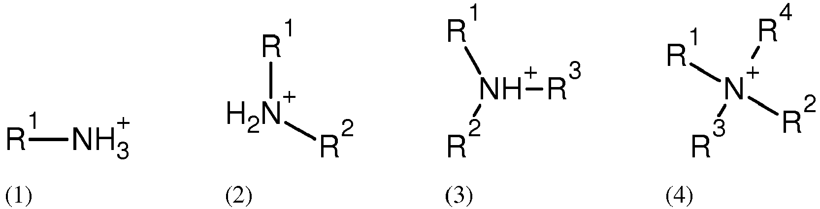

any one of R1, R2, R3 and R4 is independently selected from C1 to C15 aliphatic and C4 to C15 aromatic substituents, wherein any one, several or all hydrogens in said substituent may be replaced by halogen and wherein, if there are two or more carbons, up to half of said carbons in said substituents may be replaced by a N, S or O heteroatom, and wherein, in any one of the compounds (2) to (8), the two or more of substituents present (R1, R2, R3 and R4, as applicable) may be covalently connected to each other to form a substituted or unsubstituted ring or ring system. - According to an embodiment, B is a bivalent cation selected from any one of the compounds of formulae (9) and (10) below:

in the compound of formula (9), L is absent or an aliphatic or aromatic linker structure having 1 to 10 carbons, wherein any one, several or all hydrogens in said L may be replaced by halogen and wherein up to half of the carbons in said L may be replaced, independently, by a N, S or O heteroatom;
wherein any one of R1 and R2 is independently selected from any one of the substituents (20) to (25) below: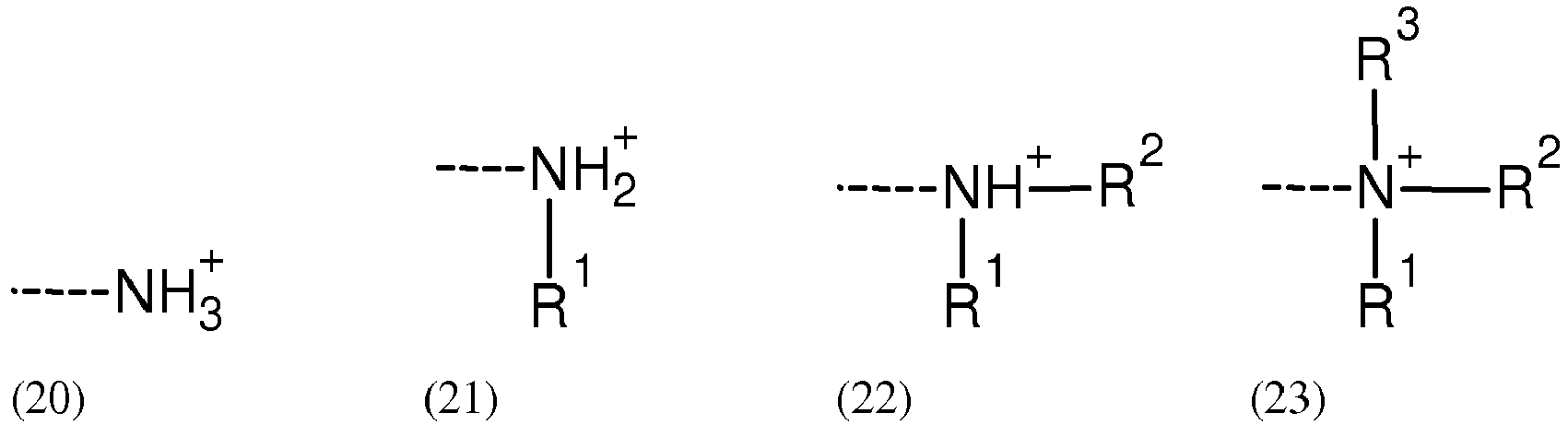
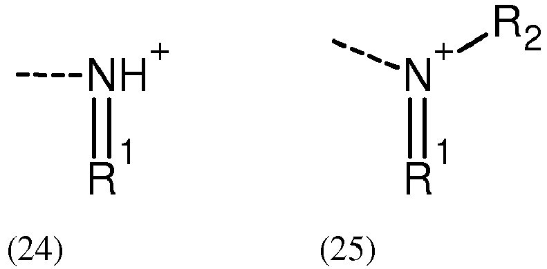
wherein R1, R2, and R3 are independently as defined above with respect to the compounds of formulae (1) to (8);
wherein R1 and R2, if they are both different from substituent (20), may be covalently connected to each other by way of their substituents R1, R2, and R3, as applicable, and wherein any one of R1, R2, and R3, if present, may be covalently connected to L or the ring structure of compound (10), independently from whether said substituent is present on R1 or R2;
and wherein, in the compound of formula (10), the circle containing said two positively charged nitrogen atoms represents an aromatic ring or ring system comprising 4 to 15 carbon atoms and 2 to 7 heteroatoms, wherein said nitrogen atoms are ring heteroatoms of said ring or ring system, and wherein the remaining of said heteroatoms may be selected independently from N, O and S and wherein R5 and R6 are independently selected from H and from substituents as R1 to R4. Halogens substituting hydrogens totally or partially may also be present in addition to said 2 to 7 heteroatoms. - If L is absent, said substituents R1 and R2 are directly connected, forming an N-N bond, as illustrated by compound (34) below.
- Preferably, if the number of carbons is in L is impair, the number of heteroatoms is smaller than the number of carbons. Preferably, in the ring structure of formula (10), the number of ring heteroatoms is smaller than the number of carbon atoms.
- According to an embodiment, in the compound of formula (9), L is an aliphatic or aromatic linker structure having 1 to 8 carbons, wherein any one, several or all hydrogens in said L may be replaced by halogen and wherein 0 to 4 carbons in said L may be replaced, independently, by a N, S or O heteroatom. Preferably, L is an aliphatic or aromatic linker structure having 1 to 6 carbons, wherein any one, several or all hydrogens in said L may be replaced by halogen and wherein 0 to 3 carbons in said L may be replaced, independently, by a N, S or O heteroatom.
- According to an embodiment, in the compound of formula (9), said linker L is free of any O or S heteroatoms. According to an embodiment, L is free of N, O and/or S heteroatoms.
- According to an embodiment, in the compound of formula (10), the circle containing said two positively charged nitrogen atoms represents an aromatic ring or ring system comprising 4 to 10 carbon atoms and 2 to 5 heteroatoms (including said two ring N-atoms).
- According to an embodiment, said ring or ring system in the compound of formula (10) is free of any O or S heteroatoms. According to an embodiment, said ring or ring system in the compound of formula (10) is free of any further N, O and/or S heteroatoms, besides said two N-ring atoms. This does not preclude the possibility of hydrogens being substituted by halogens.
- As the skilled person will understand, if an aromatic linker, compound, substituent or ring comprises 4 carbons, it comprises at least 1 ring heteroatom, so as to provide said aromatic compound.
- According to an embodiment, any one of R1, R2, R3 and R4 is independently selected from C1 to C8 aliphatic and C4 to C8 aromatic substituents wherein any one, several or all hydrogens in said substituent may be replaced by halogen and wherein, if there are two or more carbons, up to half of said carbons in said substituents may be replaced by a N, S or O heteroatom, and wherein two or more of substituents present on the same cation may be covalently connected to each other to form a substituted or unsubstituted ring or ring system.
- According to an embodiment, any one of R1, R2, R3 and R4 is independently selected from C1 to C6 aliphatic and C4 to C6 aromatic substituents wherein any one, several or all hydrogens in said substituent may be replaced by halogen and wherein, if there are two or more carbons, up to half of said carbons in said substituents may be replaced by a N, S or O heteroatom and wherein two or more of substituents present on the same cation may be covalently connected to each other to form a substituted or unsubstituted ring or ring system.
- According to an embodiment, any one of R1, R2, R3 and R4 is independently selected from C1 to C4, preferably C1 to C3 and most preferably C1 to C2 aliphatic substituents wherein any one, several or all hydrogens in said substituent may be replaced by halogen and wherein two or more of substituents present on the same cation may be covalently connected to each other to form a substituted or unsubstituted ring or ring system.
- According to an embodiment, any one of R1, R2, R3 and R4 is independently selected from C1 to C10 alkyl, C2 to C10 alkenyl and C2 to C10 alkynyl, wherein said alkyl, alkenyl and alkynyl, if they comprise 3 or more carbons, may be linear, branched or cyclic, and wherein several or all hydrogens in said substituent may be replaced by halogen.
- According to an embodiment, any one of R1, R2, R3 and R4 is independently selected from C1 to C8 alkyl, C2 to C8 alkenyl and C2 to C8 alkynyl, wherein said alkyl, alkenyl and alkynyl, if they comprise 3 or more carbons, may be linear, branched or cyclic, and wherein several or all hydrogens in said substituent may be replaced by halogen.
- According to an embodiment, any one of R1, R2, R3 and R4 is independently selected from C1 to C6 alkyl, C2 to C6 alkenyl and C2 to C6 alkynyl, wherein said alkyl, alkenyl and alkynyl, if they comprise 3 or more carbons, may be linear, branched or cyclic, and wherein several or all hydrogens in said substituent may be replaced by halogen.
- According to an embodiment, any one of R1, R2, R3 and R4 is independently selected from C1 to C4 alkyl, C2 to C4 alkenyl and C2 to C4 alkynyl, wherein said alkyl, alkenyl and alkynyl, if they comprise 3 or more carbons, may be linear, branched or cyclic, and wherein several or all hydrogens in said substituent may be replaced by halogen.
- According to an embodiment, any one of R1, R2, R3 and R4 is independently selected from C1 to C3, preferably C1 to C2 alkyl, C2 to C3, preferably C2 alkenyl and C2 to C3, preferably C2 alkynyl, wherein said alkyl, alkenyl and alkynyl, if they comprise 3 or more carbons, may be linear, branched or cyclic, and wherein several or all hydrogens in said substituent may be replaced by halogen.
- According to an embodiment, any one of R1, R2, R3 and R4 is independently selected from C1 to C4, more preferably C1 to C3 and even more preferably C1 to C2 alkyl. Most preferably, any one of R1, R2, R3 and R4 are methyl. Again, said alkyl may be completely or partially halogenated.
- According to an embodiment, A and B is a monovalent or bivalent cation, respectively, selected from substituted and unsubstituted C5 to C6 rings comprising one, two or more nitrogen heteroatoms, wherein one (for A) or two (for B) of said nitrogen atoms is/are positively charged. Substituents of such rings may be selected from halogen and from C1 to C4 alkyls, C2 to C4 alkenyls and C2 to C4 alkynyls as defined above, preferably from C1 to C3 alkyls, C3 alkenyls and C3 alkynyls as defined above. Said ring may comprise further heteroatoms, which may replace one or more carbons in said ring, in particular, heteroatoms may be selected from O, N and S. Bivalent organic cations B comprising two positively charged ring N-atoms are exemplified, for example, by the compound of formula (10) above. Such rings may be aromatic or aliphatic.
- A and B may also comprise a ring system comprising two or more rings, at least one of which being from substituted and unsubstituted C5 to C6 ring as defined as above. The elliptically drawn circle in the compound of formulae (10) may also represent a ring system comprising, for example, two or more rings, but preferably two rings. Also if A comprises two rings, further ring heteroatoms may be present, which are preferably not charged, for example.
- According to an embodiment, however, the organic cations A and B comprise one (for A), two (for B) or more nitrogen atom(s) but is free of any O or S or any other heteroatom, with the exception of halogens, which may substitute one or more hydrogen atoms in cation A and/or B.
- A preferably comprises one positively charged nitrogen atom. B preferably comprises two positively charged nitrogen atoms.
- A and B may be selected from the exemplary rings or ring systems of formulae (30) and (31) (for A) and from (32) to (34) (for B) below:


- In the organic cations A and B, hydrogens may be substituted by halogens, such as F, Cl, I, and Br, preferably F or Cl. Such a substitution is expected to reduce the hygroscopic properties of the perovskite layer or layers and is thus considered advantageous for the purpose of the present specification.
- In the methods of the invention, the perovskite layer may be applied by any one or more selected from drop casting, spin-coating, dip-coating and spray-coating, for example.
- According to an embodiment, the solar cell and/or heterojunction of the invention comprises two or more successive organic-inorganic perovskite layers, wherein said successive perovskite layers may be composed identically or wherein two or more of said layers may have a different molecular structure and/or composition. In this way, the different functions of sensitizing and/or hole transporting which are preferably achieved by the perovskite layers may be optimized and/or fine-tuned. In particular, the perovskite layer that is in contact with the scaffold structure (if a protective layer is provided (e.g. by ALD) on the scaffold structure: in contact with said protective layer), is preferably optimized with respect to its properties as a sensitizer. On the other hand, the perovskite layer or layers that is in contact with the counter electrode (or, if a protective layer is applied between the perovskite layer and the counter electrode: in contact with said perovskite layer) is preferably optimized with respect to its properties as a hole transporting material, in particular if another hole transporting material is absent, such as an organic hole transporting material.
- If there are several, different perovskite layers, the different perovskite structures may be of a different composition. Any one or more of A, B, M, N or X in the structures of formulae (I) to (IX) may be changed in order to provide a different perovskite layer having different properties, as desired. In particular, A, B, M, N or X may be changed in a subsequent layer, in order to adjust the bandgaps of the material. Different layers comprising different perovskite structures, but preferably still within the general formulae (I) to (IX), may in particular be useful to optimize a respective layer to its function (sensitizer or hole conductor).
- The solar cell of the invention preferably comprises a counter electrode. The counter electrode faces the perovskite towards the inside of the cell, and for example to a substrate towards (in direction of) the outside of the cell, if such substrate is present. The counter electrode generally comprises a catalytically active material, suitable to provide electrons and/or fill holes towards the inside of the device. The counter electrode may thus comprise one or more materials selected from (the group consisting of) Pt, Au, Ni, Cu, Ag, In, Ru, Pd, Rh, Ir, Os, C, conductive polymer and a combination of two or more of the aforementioned, for example. Conductive polymers may be selected from polymers comprising polyaniline, polypyrrole, polythiophene, polybenzene, polyethylenedioxythiophene, polypropylenedioxythiophene, polyacetylene, and combinations of two or more of the aforementioned, for example.
- Of course, if there is a protective layer as discussed below between the counter electrode and the outermost perovskite layer, the counter electrode faces, towards the inside of the cell, said protective layer, which protective layer in turn faces, towards the inside of the cell, said perovskite layer, or a hole conductor layer, is such a layer is present.
- The counter electrode may be applied as is conventional, for example by thermal evaporation of the counter electrode material onto the perovskite layer.
- The counter electrode is preferably connected to a current collector, which is then is connected to the external circuit, as the conductive support on the other, opposed side of the device. As on the opposed side of the device, a conductive support such as conductive glass or plastic may be electrically connected to the counter electrode. In this case, the device has two opposed support or protective layers, which encase the solar cell, for example.
- The solar cell of the invention is preferably a solid state solar cell. By avoiding an electrolyte, the disadvantages of electrolytes, such as loss due to solvent evaporation, electrolyte leakage, disadvantages associated with the use of redox shuttles, for example, can be avoided.
- According to an embodiment, the solar cell and/or heterojunction of the invention cell lacks and/or is substantially or totally free of a separate, non-perovskite hole transporting material layer between said perovskite layer and said counter electrode. Preferably, the entire device is substantially free of a substantially organic charge (and/or hole) transporting material and/or free of an organic hole transport layer. By "organic hole transporting material", "organic charge transporting material", and the like, is meant any material or composition comprising an organic compound, wherein charges are transported by electron or hole movement (electronic motion) across said organic compound, said electronic compound being conductive. Organic hole transport materials are different from electrolytes in which charges are transported by diffusion of molecules.
- It is surprising that a device lacking a non-perovskite hole transport layer is functional. Typically, solid state, sensitizer-based solar cells use a substantially organic hole transporting material in order to remove holes from the sensitizer and/or provide new electrons from the counter electrode to the sensitizer. The solar cell of the invention may and thus function without such an organic charge transporting material layer. A prominent example of an organic hole transporting material that is frequently used in prior art solid state solar cells is 2,2',7,7'-tetrakis(N,N-di-methoxyphenyamine)-9,9'-spirobifluorene (Spiro-MeOTAD). Preferably, the solar cell of the invention lack and/or is free of Spiro-MeOTAD. In
W02007107961 , a liquid organic hole conductor is disclosed. Preferably, the solar cell of the invention lacks and/or is free of a liquid hole conductor as disclosed inWO2007107961 . - According to an embodiment, said counter electrode and/or metal layer is in direct contact with said perovskite layer and/or not separated by any further layer or medium from said perovskite layer. However, this does not exclude the possibility of a metal oxide protective layer of up to 1.5 nm thickness, which may be provided between said counter electrode and said perovskite layer, as specified elsewhere in this specification. Preferably, said counter electrode and/or metal layer is in direct electric contact with said perovskite layer, wherein electrons move from the counter electrode to the perovskite material, optionally across said protective layer.
- Furthermore, while a non-perovskite, for example an organic hole transporting material may be absent in the device, the invention also encompasses solar cells in which a hole transport material, for example an inorganic hole transport layer or an organic hole transport layer comprising a material as defined and/ specified above, is present. An organic or inorganic hole transport material, if present, is preferably provided between the perovskite layer or layers and the counter electrode. If there are more than one perovskite layers, an inorganic and/or organic hole transporting material is preferably provided between the outermost perovskite layer and the counter electrode. In accordance with this embodiment, the organic or inorganic hole transport material is preferably a non-perovskite hole transport material.
- It is noted that the term "organic" in expressions "organic hole transport material", "organic hole transport layer", "organic charge transport material" and the like does not exclude the presence of further components. Further components may be selected from (a) one or more dopants, (b) one or more solvents, (c) one or more other additives such as ionic compounds, and (c) combinations of the aforementioned components, for example. In the organic charge transport material, such further components may be present in amounts of 0-30wt.%, 0-20wt.%, 0-10wt.%, most preferably 0-5wt.%.
- According to an embodiment, the solar cell and/or heterojunction of the invention comprises a metal oxide layer comprising a material selected from Mg-oxide, Hf-oxide, Ga-oxide, In-oxide, Nb-oxide, Ti-oxide, Ta-oxide, Y-oxide and Zr-oxide and having a thickness of not more than 1.5 nm, more preferably not more than 1 nm. Ga-oxide is preferred. Said metal oxide layer is in particular "buffer layer", also referred to as a "protective layer", which reduces or prevents recombination of photo generated electrons with the perovskite material, for example.
- According to an embodiment, of the solar cell and/or heterojunction of the invention said metal oxide layer is a buffer layer and is provided on said scaffold structure by atomic layer deposition (ALD). Preferably, 2 to 7, preferably 3 to 5 and most preferably about 4 layers are deposited by ALD so as to provide said protective layer. Accordingly, said metal oxide layer is preferably a metal oxide multilayer.
- Preferably, said metal oxide layer has a thickness of 1.5 nanometer (nm) or less (≤), preferably < 1.2 nm and most preferably ≤ 1 nm. According to an embodiment, said metal oxide layer has a thickness of 0.2 to 0.8 nm, preferably 0.3 to 0.7 nm, most preferably 0.4 to 0.6 nm.
- The thickness of the metal oxide layer is preferably such that a tunneling of the electrons of the photo-excited perovskite into the conducting support layer and/or the scaffold structure is still possible. Tunneling is only possible if a certain thickness of the layer is not exceeded. In this case, electrons can go through the metal oxide layer, as they are not or only to a minor or acceptable extent prevented from transferring to the semiconductor material.
- The protective layer is preferably as is disclosed in the pending international application
PCT/IB2011/055550, filed on December 8, 2011 - The solar cell of the invention may comprise 0, 1, two or even more protective layers selected independently from protective layers as defined above. According to an embodiment, the protective layer is provided between the scaffold structure and the perovskite. If there are more than one perovskite layers, the protective layer is preferably provided between the scaffold layer and the innermost perovskite layer. In case there are several perovskite layers in the device of the invention, the innermost perovskite layer is the one that is closest to the scaffold structure and/or farthest from the counter electrode; and the outermost perovskite layer is the layer that is farthest from the scaffold structure and closest to the counter electrode.
- In accordance with an embodiment, a protective layer is provided between the perovskite layer and the counter electrode. If there are several perovskite layers, the protective layer is preferably provided between the outermost perovskite layer and the counter electrode. In other words, the counter electrode is either directly in contact with the (outermost) perovskite layer or with the protective layer towards the inside of the cell. In the latter case, the protective layer is in contact with the (outermost) perovskite layer.
- Schematically, the present solar cell preferably comprises and/or consists of the following layers:
- (2) conductive support and/or charge collector;
- (3) scaffold structure;
- (i) optional protective layer;
- (4) perovskite layer;
- (4.1-4.n) optional n further perovskite layers, n being an integer of 1 to 10;
- (ii) optional hole conductor layer;
- (iii) optional protective layer;
- (5) counter electrode.
- The method of the invention comprises the step of applying one or more organic-inorganic perovskite layer on said scaffold structure. The perovskite layer may be applied by any suitable process. According to an embodiment, the one or more perovskite layers are applied by any one or a combination of drop costing, spin-coating, dip-coating and spray-coating.
- According to an embodiment, the method of the invention comprises, consists essentially of or consists of the steps of the steps of providing a conducting support layer on which a surface-increasing scaffold structure is provided; applying one or more organic-inorganic perovskite layer on said scaffold structure; and, applying a counter electrode. Preferably, these steps are conducted in this order, with further or other steps being conducted before, after or within these steps without changing the order of the steps.
- According to a preferred embodiment of the methods of the invention, said counter electrode is applied on said perovskite layer, or, if there are several such layers, on the outermost of said perovskite layers. If a hole conducting material used (for example an organic or inorganic) the latter is preferably provided between said outermost perovskite layer and said counter electrode. In this case, the methods of the invention comprise the step of applying a counter electrode on said hole conductor layer.
- According to an embodiment, the method of the invention comprises one or more steps of applying one or more protective layers, in accordance with indications given elsewhere in this specification with respect to protective layers.
-
Figure 1A shows an exemplarysolar cell 1 of the invention, in which 2 represents a conductive support, which may be an FTO glass as shown, 3 represents the scaffold structure, which, inFig. 1A is indicated to be made from TiO2, 4 represents the perovskite layer and 5 is the counter electrode, which may exemplary be made from a metal, as shown inFig. 1A . - The present invention will now be illustrated by way of examples. These examples do not limit the scope of this invention, which is defined by the appended claims.
- CH3NH3I was synthesized by reacting 30 mL methylamine (40% in methanol, TCI) and 32.3 mL of hydroiodic acid (57 wt% in water, Aldrich) in a 250 mL round bottomed flask at 0 °C for 2 h with stirring. The precipitate was recovered by putting the clear solution on a roti-vapor and carefully removed the solvents at 50 °C. The yellowish raw product, methylammonium iodide (CH3NH3I), was washed with diethyl ether by stirring the solution for 30 min, which was repeated three times, and then finally recrystallized from a mixed solvent of diethyl ether and ethanol. After filtration, the solid was collected and dried at 60 °C in vacuum oven for 24 h.
- The synthesis of the nanosheets was followed a typical experimental procedure31. Ti(OBu)4 (10 mL, 98%) and hydrofluoric acid (0.8 mL, 47%) solution mixed in a 150 mL dried Teflonautoclave which was kept at 180°C for 24 h to yield well-defined rectangular sheet-like structures with a side length of 30 nm and a thickness of 7 nm. After the reaction was cooled to room temperature, the white powder was separated by high-speed centrifugation and washed with ethanol followed by distilled water for several times.
- Caution: Hydrofluoric acid is extremely corrosive and a contact poison, it should be handled with extreme care! Hydrofluoric acid solution is stored in Teflon containers in use.
- Thin dense TiO2 layer of ∼100 nm thickness was deposited onto a SnO2:F conducting glass substrate (15Ω/cm, Pilkington) by spray pyrolysis method 32. The deposition temperature of TiO2 compact layer was 450 °C. Nanopores TiO2 film ( ∼ 0.5 µm thick) was prepared by spin coating method onto this substrate using the TiO2 nanosheets with 001 dominant facets. The TiO2 layer was annealed at 500 °C for 30 min in air. The substrate was immersed in 40 mM TiCl4 aqueous solutions for 30 min at 70 °C and washed with distilled water and ethanol, followed by annealing at 500 °C for 30 min in air.
- The synthesis of CH3NH3PbI3 on the TiO2 surface was carried out by dropping on the TiO2 film a 40 wt% precursor solution of CH3NH3I and PbI2 in γ-butyrolactone and film formation by spin coating (2000 rpm, 30 sec) in the glove box.
- The film coated on the TiO2 changed its color with drying at room temperature, indicating the formation of CH3NH3PbI3 in the solid state. The CH3NH3PbI3 film was annealed under argon for 15min at 100°C.
- Finally the counter electrode was deposited by thermal evaporation of gold under a pressure of 5×10⁻⁵ Torr. The active area was 0.12 cm2. After the preparation, the cells were allowed to expose in air.
- Photovoltaic measurements employed an AM 1.5 solar simulator equipped with a 450W xenon lamp (Model No. 81172, Oriel). Its power output was adjusted to match AM 1.5 global sunlight (100 mW/cm2) by using a reference Si photodiode equipped with an IR-cutoff filter (KG-3, Schott) in order to reduce the mismatch between the simulated light and AM 1.5 (in the region of 350-750 nm) to less than 2% with measurements verified at two PV calibration laboratories [ISE (Germany), NREL (USA)]. I-V curves were obtained by applying an external bias to the cell and measuring the generated photocurrent with a Keithley model 2400 digital source meter. The voltage step and delay time of photocurrent were 10 mV and 40 ms, respectively. A similar data acquisition system was used to determine the monochromatic incident photon- to-electric current conversion efficiency. Under full computer control, light from a 300 W xenon lamp (ILC Technology, U.S.A.) was focused through a Gemini-180 double monochromator (Jobin Yvon Ltd., U.K.) onto the photovoltaic cell under test. The monochromator was incremented through the visible spectrum to generate the IPCE (λ) as defined by IPCE (λ)) = 12400(Jsc/λϕ), where λ is the wavelength, Jsc is short-circuit photocurrent density (mA cm-2), and ϕ is the incident radiative flux (mW cm-2). Photovoltaic performance was measured by using a metal mask with an aperture area of 0.49 cm2.
- The cross section of the device was measured by Zeiss Jemini FEG-SEM, using 5kV with magnification of 250KX.
- The synthesis of CH3NH3PbI3 on the TiO2 surface was carried out by dropping on the TiO2 film a 40 wt% precursor solution of CH3NH3I and PbI2 in γ-butyrolactone and film formation by spin coating. CH3NH3I was synthesized from HI by reaction with 40% methylamine in methanol solution and recrystallization. The film coated on the TiO2 changed its color with drying at room temperature, indicating the formation of CH3NH3PbI3 in the solid state.
-
Figures 1A and 1B present a scheme of the device structure and its energy level diagram. The conduction and valence bands of the CH3NH3PbI3 permit electron injection and hole transportation to the TiO2 and the gold respectively. The bottom layer is composed of compact TiO2 and TiO2 nanosheets with exposed (001) facets layers acting as electron collectors. The light is absorbed by CH3NH3PbI3 thin film, which was made by spin coating technique. A gold contact was eveporated on top of the CH3NH3PbI3 thin film. -
Figure 2 shows high resolution scaning electron microscopy (HR-SEM) image of the cross section of the solar cell. Since the organo lead halide perovskite is depositied as thin layer on top of the TiO2 nanosheets it is hard to distinguish between the TiO2 and the perovskite. -
Figure 3A exhibits J-V characteristics of the CH3NH3PbI3 heterojunction photovoltaic cell under 1 sun illumination. The organo lead perovskite heterojunction solar cell produces an open-circuit voltage (Voc) of 0.631 V, a short circuit current density (Jsc) of 16.1mA cm-2 and a fill factor of 57% corresponding to a power conversion efficiency (PCE) of 5.5% under 1 sun intensity (Table 1). It is important to note that the power conversion effiency under 10% sun was 7.28% with Jsc of 2.14 mA cm-2, a fill factor of 62% and Voc of 0.565 V. - The incident photon to current conversion efficiency (IPCE) specifies the ratio of extracted electrons to incident photons at a given wavelength. The IPCE spectrum (
Figure 3B ) is plotted as a function of wavelength of the light. The solid state CH3NH3PbI3 heterojunction solar cell shows a good response from the visible through 800nm wavelength, the IPCE spectrum is reaching its maximum of 90% at wavelength of 400nm until 540nm while it is decreasing till 780nm wavelength. Integration of the IPCE spectrum over the AM1.5 solar emission yields a photocurrent density of 16.2 mA/cm2, in good agreement with the measured values.Table 1: photovoltaic characteristic of perovskite cell Sun Intensity Jsc (mA/cm2) Voc (mV) FF η (%) 10 2.1 565.8 0.62 7.28 100 16.1 631.6 0.57 5.5 - In summary the organo lead perovskite act as an efficient sensitizer and hole transport material by that we are eliminate the use of hole conductor. The perovskite is stable at ambient air and it can be deposited by low cost technique. This finding opens the way for high efficiency low cost photovoltaic cells.
-
- 1 Huynh, W. U., Dittmer, J. J.; Alivisatos, A P ,Science, 2002,295,2425.
- 2 I. Gur, N. A. Fromer, M. I Geier, A. P Alivisatos, Science, 2005, 310, 462 .
- 3 W. J. E. Beek, M. M Wienk, R. A. J. Janssen, Adv. Func. Mater. 2006, 16, 1112.
- 4 J. M. Luther, M. Law, M. C. Beard, Q. Song, M. O. Reese, R. J. Ellingson, A. J. Nozik, Nano lett. 2008, 8, 3488.
- 5 W. Ma, J. M. Luther, H.Zheng, Y.Wu, A. P. Alivisatos, Nano lett. 2009, 9,1699.
- 6 R. Plass, S.Pelet, J. Krueger, M. Grätzel, U. Bach, J. Phys. Chem. B, 2002, 106, 7578.
- 7 B. Sun, A. T. Findikoglu, M. Sykora, D. J. Werder, V. I. Klimov, Nano lett. 2009, 9, 1235.
- 8 J. M. Luther, M. Law, Q. Song, C. L. Perkins, M. C. Beard, A. J. Nozik, ACS Nano, 2008, 2,271.
- 9 S. Zhang, P. W. Cyr, S. A. McDonald, G. Konstantatos, E. H. Sargent, Appl. Phys. Lett. 2005, 87, 233101.
- 10 B.-R. Hyun, Y.-W. Zhong, A. C. Bartnik, L. Sun, H. D. Abrua, F. W. Wise, J. D. Goodreau, J. R. Matthews, T. M. Leslie, F. Borrelli, ACS Nano, 2008, 2, 2206.

- 11 D. Ratan, T. Jiang, D. A. Barkhouse, W. Xihua, G. P.-A. Andras, B. Lukasz, L. Larissa, E. H. Sargent, J. Amer. Chem. Soc., 2010, 132, 5952.
- 12 J. M. Luther, J. Gao, M. T. Lloyd, O. E. Semonin, M. C. Beard, A. J. Nozik, Adv. Mater. 2010, 22, 3704.
- 13 A. G. Pattantyus-Abraham, I. J. Kramer, A. R. Barkhouse, X. Wang, G. Konstantatos, R. Debnath, L. Levina, I. Raabe, M. K. Nazeeruddin, M. Gratzel, E. H. Sargent, ACS Nano. 2010, 4(6), 3374.
- 14 H. Liu, J. Tang, I. J. Kramer, R. Debnath, G. I. Koleilat, X. Wang, A. Fisher, R. Li, L. Brzozowski, L. Levina, E. H. Sargent, Adv. Mater. 2011, 23, 3832.
- 15 J. Gao, J. M. Luther, O. E. Semonin, R. J. Ellingson, A. J. Nozik, M. C. Beard, Nano Lett., 2011, 11 (3), pp 1002.
- 16 J. Gao, C. L. Perkins, J. M. Luther, M. C. Hanna, H.Y. Chen, O. E. Semonin, A. J. Nozik, R. J. Ellingson, M. C. Beard, Nano Lett., 2011, 11 (8), pp 3263.
- 17 D. A. R. Barkhouse, R. Debnath, I. J. Kramer, D. Zhitomirsky, A. G. Pattantyus-Abraham, L. Levina, L. Etgar, M. Grätzel, Edward H. Sargent, Adv. Mater., 2011, 23, 3134.
- 18 X. Wang, G. I. Koleilat, J. Tang, H. Liu, I. J. Kramer, R. Debnath, L. Brzozowski, D. A. R. Barkhouse, L. Levina, S. Hoogland, E. H. Sargent, Nature photonics, 2011, 5, 480.
- 19 K. S. Leschikies, T. J. Beatty, M. S. Kang, D. J. Norris, E. S. Aydil, ACS Nano, 2009, 3(11), 3638.
- 20 Lioz Etgar, Wei Zhang, Stefanie Gabriel, Stephen G. Hickey, Md K. Nazeeruddin , Alexander Eychmüller, Bin Liu, Michael Grätzel. Advanced Materials, 2012, 24(16), 2202-2206.
- 21 Lioz Etgar, Thomas Moehl, Stefanie Tscharntke, Stephen G. Hickey, Alexander Eychmüller and Michael Grätzel. ACS Nano, 6 (4), 3092-3099, 2012.
- 22 F. W. Wise, Acc. Chem. Res. 2000, 33, 773.
- 23 J. B. Sambur, T. Novet, B. A. Parkinson, Science, 2010, 330, 63.
- 24 Akihiro Kojima, Masashi Ikegami, Kenjiro Teshima, and Tsutomu Miyasaka, Chem. Lett. 2012,41,397.
- 25 C. I. Covaliu, L. C. Chioaru, L. Craciun, O. Oprea, I. Jitaru, Optoelectronics and advanced materials , 5 (10), 2011, 1097.
- 26 C.R. Kagan, D. B. Mitzi, C. D. Dimitrakopoulos, Science 286, 945, 1999.
- 27 D.B Mitzi, C.A. Feild, Z. Schlesinger, R.B. Laibowitz, J.Solid State Chem. 114, 159, 1995.
- 28 Akihiro Kojima, Kenjiro Teshima, Yasuo Shirai, and Tsutomu Miyasaka, J.Am. Chem. Soc. 2009, 131, 6050-6051.
- 29 Jeong-Hyoek Im, Jaehoon Chung , Seung-Joo Kim , Nam-Gyu Park, Nanoscale Research Letters, 2012, 7:353.
- 30 Jeong-Hyeok Im, Chang-Ryul Lee, Jin-Wook Lee, Sang-Won Park and Nam-Gyu Park, nanoscale, 2011, 3, 4088.
- 31 X. Han, Q. Kuang, M. Jin, Z. Xie, L. Zheng, J. Am. Chem. Soc., 2009, 131 (9), 3152.
- 32 Moon, S. J.; Yum, J. H.; Humphry-Baker, R.; Karlsson, K. M.; Hagberg, D. P.; Marinado, T.; Hagfeldt, A.; Sun, L. C.; Grätzel, M.; Nazeeruddin, M. K. J. Phys. Chem. C 2009, 113, 16816.
Claims (15)
- A solid-state solar cell (1) comprising a conducting support layer (2) and a surface-increasing scaffold structure (3), wherein one or more organic-inorganic perovskite layer (4) is provided on said scaffold structure or on a protective layer that is optionally provided on said scaffold structure, and wherein a counter electrode and/or metal layer (5) is provided in electric contact with said perovskite layer.
- The solar cell of claim 1, wherein said solar cell lacks a separate, non-perovskite hole transporting material layer between said perovskite layer and said counter electrode.
- The solar cell of any one of the preceding claims, wherein said organic-inorganic perovskite layer (4) comprises a perovskite-structure of the formula (I), (II), (III), and/or (IV) below,
A2MX4 (I)
AMX3 (II)
ANX4 (III)
BMX4 (IV)
wherein,A is an organic, monovalent cation selected from primary, secondary, tertiary or quaternary organic ammonium compounds, including N-containing heterorings and ring systems, A having from 1 to 15 carbons and 1-20 heteroatoms;B is an organic, bialent cation selected from primary, secondary, tertiary or quaternary organic ammonium compounds having from 1 to 15 carbons and 2-20 heteroatoms and having two positively charged nitrogen atoms;M is a divalent metal cation selected from the group consisting of Cu2+, Ni2+, Co2+, Fe2+, Mn2+, Cr 2+, Pd2+, Cd2+, Ge2+, Sn2+, Pb2+, Eu2+, or Yb2+;N is selected from the group of Bi3+ and Sb3+; andthe three or four X are independently selected from l-, Br-, I-, NCS-, CN-, and NCO-. - The solar cell of any one of the preceding claims, wherein said organic-inorganic perovskite layer (4) comprises a perovskite-structure of any one of the formulae (V), (VI), (VII), (VIII), (IX) and (X);
APbX3 (V)
ASnX3 (VI)
A2PbX4 (VII)
A2SnX4 (VIII)
BPbX4 (IX)
BSnX4 (X)
wherein A, B and X are as defined above. - The solar cell of any one of claims 3 and 4, wherein X is selected from Br- and I-.
- The solar cell of any one of claims 3 to 5, wherein A is a monovalent cation selected from any one of the compounds of formulae (1) to (8) below:

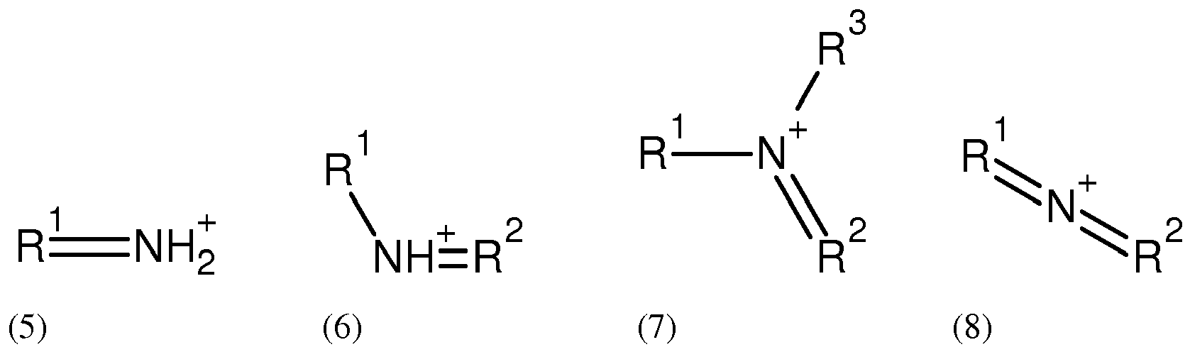
any one of R1, R2, R3 and R4 is independently selected from C1 to C15 aliphatic and C4 to C15 aromatic substituents, wherein any one, several or all hydrogens in said substituent may be replaced by halogen and wherein, if there are two or more carbons, up to half of said carbons in said substituents may be replaced by a N, S or O heteroatom, and wherein, in any one of the compounds (2) to (8), the two or more of the substituents present may be covalently connected to each other to form a substituted or unsubstituted ring or ring system. - The solar cell of any one of claims 3 to 6, wherein B is a bivalent cation selected from any one of the compounds of formulae (9) and (10) below:

in the compound of formula (9), L is an aliphatic or aromatic linker structure having 1 to 10 carbons, wherein any one, several or all hydrogens in said L may be replaced by halogen and wherein 0 to 5 carbons in said L may be replaced, independently, by a N, S or O heteroatom;
wherein the ring in compound (10) represents a aliphatic or aromatic ring or ring system comprising 4 to 15 carbons and 2 to 7 heteroatoms, including said two N-heteroatoms;
wherein any one of R1 and R2 is independently selected from any one of the substituents (20) to (25) below:

wherein R1, R2, and R3 are independently as defined in Claim 6;
wherein R1 and R2, if they are both different from substituent (20), may be covalently connected to each other by way of their substituents R1, R2, and R3, as applicable, and wherein any one of R1, R2, and R3, if present, may be covalently connected to L or the ring structure of compound (10), independently from whether said substituent is present on R1 or R2;
and wherein, in the compound of formula (10), the circle containing said two positively charged nitrogen atoms represents an aromatic ring or ring system comprising 4 to 15 carbon atoms and 2 to 7 heteroatoms, wherein said nitrogen atoms are ring heteroatoms of said ring or ring system, and wherein R5 and R6 are independently selected from H and from substituents as R1 to R4. - The solar cell of any one of the preceding claims, wherein said surface-increasing scaffold structure (3) is made from and/or comprises one selected from the group consisting of a semiconductor material, a conducting material and a non-conducting material.
- The solar cell of any one of the preceding claims, wherein the surface area per gram ratio of said scaffold structure (3) is in the range of 20 to 200 m2/g, preferably 30 to 150 m2/g, and most preferably 60 to 120 m2/g.
- The solar cell of any one of the preceding claims, wherein said scaffold structure (3) comprises and/or is prepared from nanoparticles, such as nanosheets.
- The solar cell of any one of the preceding claims, wherein said scaffold structure (3) is nanostructured and/or nanoporous.
- The solar cell of any one of the preceding claims, further comprising a metal oxide layer comprising a material selected from Mg-oxide, Hf-oxide, Ga-oxide, In-oxide, Nb-oxide, Ti-oxide, Ta-oxide, Y-oxide and Zr-oxide and having a thickness of not more than1 nm.
- The solar cell of any one of the preceding claims, comprising two or more successive organic-inorganic perovskite layers (4), wherein said successive perovskite layers may be composed identically or wherein two or more of said layers may have a different molecular structure and/or composition.
- A solid state heterojunction comprising a conducting support layer (2), on which a surface-increasing scaffold structure (3) is provided, wherein an organic-inorganic perovskite layer (4) is provided on said scaffold structure.
- A method of preparing a solid state solar cell, the method comprising the steps of:- providing a conducting support layer (2) on which a surface-increasing scaffold structure (3) is provided;- applying one or more organic-inorganic perovskite layer (4) on said scaffold structure or on a protective layer that may be present on said scaffold structure by any one or more selected from spin-coating, dip-coating and spray-coating; and,- applying a counter electrode.
Priority Applications (8)
| Application Number | Priority Date | Filing Date | Title |
|---|---|---|---|
| EP12179323.6A EP2693503A1 (en) | 2012-08-03 | 2012-08-03 | Organo metal halide perovskite heterojunction solar cell and fabrication thereof |
| JP2015524882A JP6386458B2 (en) | 2012-08-03 | 2013-07-24 | Organometallic halide perovskite heterojunction solar cell and method for producing the same |
| EP13773384.6A EP2880698B9 (en) | 2012-08-03 | 2013-07-24 | Organo metal halide perovskite heterojunction solar cell and fabrication thereof |
| KR1020157004662A KR102179571B1 (en) | 2012-08-03 | 2013-07-24 | Organo metal halide perovskite heterojunction solar cell and fabrication thereof |
| CN201380049314.4A CN104737320B (en) | 2012-08-03 | 2013-07-24 | Organic metal halide perovskite heterojunction solar battery and its manufacture |
| AU2013298165A AU2013298165B2 (en) | 2012-08-03 | 2013-07-24 | Organo metal halide perovskite heterojunction solar cell and fabrication thereof |
| PCT/IB2013/056080 WO2014020499A1 (en) | 2012-08-03 | 2013-07-24 | Organo metal halide perovskite heterojunction solar cell and fabrication thereof |
| US14/419,171 US20150200377A1 (en) | 2012-08-03 | 2013-07-24 | Organo metal halide perovskite heterojunction solar cell and fabrication thereof |
Applications Claiming Priority (1)
| Application Number | Priority Date | Filing Date | Title |
|---|---|---|---|
| EP12179323.6A EP2693503A1 (en) | 2012-08-03 | 2012-08-03 | Organo metal halide perovskite heterojunction solar cell and fabrication thereof |
Publications (1)
| Publication Number | Publication Date |
|---|---|
| EP2693503A1 true EP2693503A1 (en) | 2014-02-05 |
Family
ID=49304031
Family Applications (2)
| Application Number | Title | Priority Date | Filing Date |
|---|---|---|---|
| EP12179323.6A Withdrawn EP2693503A1 (en) | 2012-08-03 | 2012-08-03 | Organo metal halide perovskite heterojunction solar cell and fabrication thereof |
| EP13773384.6A Active EP2880698B9 (en) | 2012-08-03 | 2013-07-24 | Organo metal halide perovskite heterojunction solar cell and fabrication thereof |
Family Applications After (1)
| Application Number | Title | Priority Date | Filing Date |
|---|---|---|---|
| EP13773384.6A Active EP2880698B9 (en) | 2012-08-03 | 2013-07-24 | Organo metal halide perovskite heterojunction solar cell and fabrication thereof |
Country Status (7)
| Country | Link |
|---|---|
| US (1) | US20150200377A1 (en) |
| EP (2) | EP2693503A1 (en) |
| JP (1) | JP6386458B2 (en) |
| KR (1) | KR102179571B1 (en) |
| CN (1) | CN104737320B (en) |
| AU (1) | AU2013298165B2 (en) |
| WO (1) | WO2014020499A1 (en) |
Cited By (31)
| Publication number | Priority date | Publication date | Assignee | Title |
|---|---|---|---|---|
| WO2014180780A1 (en) | 2013-05-06 | 2014-11-13 | Greatcell Solar S.A. | Organic-inorganic perovskite based solar cell |
| CN104447349A (en) * | 2014-12-11 | 2015-03-25 | 福建江夏学院 | Hybrid perovskite material |
| WO2015140548A1 (en) * | 2014-03-18 | 2015-09-24 | Isis Innovation Limited | Hole conduction layer |
| WO2015160838A1 (en) * | 2014-04-15 | 2015-10-22 | Northwestern University | Lead-free solid-state organic-inorganic halide perovskite photovoltaic cells |
| US9231136B2 (en) | 2014-04-29 | 2016-01-05 | National Central University | Method for preparing perovskite film and solar cell thereof |
| WO2016019124A1 (en) * | 2014-08-01 | 2016-02-04 | Hunt Energy Enterprises, L.L.C. | Method of formulating perovskite solar cell materials |
| GB2528831A (en) * | 2014-06-05 | 2016-02-10 | Univ Swansea | Perovskite pigments for solar cells |
| WO2016043002A1 (en) * | 2014-09-16 | 2016-03-24 | 株式会社クレハ | Organic-inorganic hybrid compound, amine hydroiodide salt, composition for photoelectric conversion element, and photoelectric conversion element |
| WO2016072439A1 (en) * | 2014-11-07 | 2016-05-12 | 富士フイルム株式会社 | Photoelectric conversion element and solar cell |
| WO2016110851A1 (en) * | 2015-01-07 | 2016-07-14 | Yissum Research Development Company Of The Hebrew University Of Jerusalem Ltd | Self-assembly of perovskite for fabrication of transparent devices |
| US9431613B2 (en) | 2014-08-13 | 2016-08-30 | National Tsing Hua University | Method of fabricating perovskite solar cell |
| WO2016163985A1 (en) * | 2015-04-06 | 2016-10-13 | Tao Xu | Perovskite photovoltaic device |
| DE102015213100A1 (en) * | 2015-07-13 | 2017-01-19 | Technische Universität Dresden | Lead-free light-absorbing compounds, processes for their preparation and their use in optoelectronic components |
| EP3144989A1 (en) | 2015-09-16 | 2017-03-22 | ThyssenKrupp Steel Europe AG | Solid body photovoltaic element |
| EP3167496A1 (en) * | 2014-07-11 | 2017-05-17 | Ecole Polytechnique Federale de Lausanne (EPFL) | Template enhanced organic inorganic perovskite heterojunction photovoltaic device |
| EP3168877A1 (en) | 2015-11-13 | 2017-05-17 | TWI Limited | A wire shaped coaxial photovoltaic solar cell |
| JP2017516316A (en) * | 2013-03-21 | 2017-06-15 | ボード オブ トラスティーズ オブ ミシガン ステート ユニバーシティ | Transparent energy capture device |
| EP3185323A1 (en) * | 2014-05-09 | 2017-06-28 | Novaled GmbH | Doped perovskites and their use as active and/or charge transport layers in optoelectronic devices |
| JP2017530549A (en) * | 2014-12-08 | 2017-10-12 | エルジー・ケム・リミテッド | Organic-inorganic hybrid perovskite compound, method for producing the same, and solar cell including the same |
| US9803136B2 (en) | 2012-02-21 | 2017-10-31 | Northwestern University | Liquid electrolyte-free, solid-state solar cells with inorganic hole transport materials |
| EP3136450A4 (en) * | 2014-04-28 | 2017-11-08 | Research & Business Foundation Sungkyunkwan University | Perovskite solar cell and manufacturing method therefor |
| EP3131653A4 (en) * | 2014-03-17 | 2017-11-08 | Monash University | Improved precipitation process for producing perovskite-based solar cells |
| US9966198B2 (en) | 2014-04-24 | 2018-05-08 | Northwestern University | Solar cells with perovskite-based light sensitization layers |
| CN108832005A (en) * | 2018-06-25 | 2018-11-16 | 陕西师范大学 | High efficiency CsPbBr is prepared using single source thermal evaporation3The method of inorganic perovskite battery |
| US10388898B2 (en) | 2017-06-05 | 2019-08-20 | Board Of Trustees Of Northern Illinois University | Doped perovskite having improved stability, and solar cells made thereof |
| US10457148B2 (en) | 2017-02-24 | 2019-10-29 | Epic Battery Inc. | Solar car |
| US10587221B2 (en) | 2017-04-03 | 2020-03-10 | Epic Battery Inc. | Modular solar battery |
| US10892106B2 (en) | 2016-05-13 | 2021-01-12 | University of Pittsburgh—of the Commonwealth System of Higher Education | Highly stable electronic device employing hydrophobic composite coating layer |
| CN114250473A (en) * | 2022-03-01 | 2022-03-29 | 青岛理工大学 | Iron oxide based Z-shaped heterojunction composite photo-anode film and preparation method and application thereof |
| EP3413365B1 (en) | 2012-09-18 | 2022-06-29 | Oxford University Innovation Limited | Optoelectronic device |
| US11489082B2 (en) | 2019-07-30 | 2022-11-01 | Epic Battery Inc. | Durable solar panels |
Families Citing this family (98)
| Publication number | Priority date | Publication date | Assignee | Title |
|---|---|---|---|---|
| US10303035B2 (en) | 2009-12-22 | 2019-05-28 | View, Inc. | Self-contained EC IGU |
| US10038150B2 (en) | 2011-02-25 | 2018-07-31 | Ecole Polytechnique Federale De Lausanne (Epfl) | Metal complexes for use as dopants and other uses |
| GB201208793D0 (en) | 2012-05-18 | 2012-07-04 | Isis Innovation | Optoelectronic device |
| ES2568623T3 (en) | 2012-05-18 | 2016-05-03 | Isis Innovation Limited | Optoelectric device comprising porous shell material and perovskites |
| EP3010054B1 (en) | 2012-05-18 | 2019-02-20 | Oxford University Innovation Limited | Optoelectronic device |
| EP3842613A1 (en) | 2012-08-23 | 2021-06-30 | View, Inc. | Photonic powered electrochromic devices |
| TWI514606B (en) * | 2012-09-12 | 2015-12-21 | Korea Res Inst Chem Tech | Solar cell comprising light absorption structure |
| CN105593206B (en) | 2013-10-02 | 2017-10-10 | 默克专利有限公司 | Hole mobile material |
| US9520512B2 (en) | 2013-11-26 | 2016-12-13 | Hunt Energy Enterprises, L.L.C. | Titanate interfacial layers in perovskite material devices |
| US9136408B2 (en) | 2013-11-26 | 2015-09-15 | Hunt Energy Enterprises, Llc | Perovskite and other solar cell materials |
| US9416279B2 (en) | 2013-11-26 | 2016-08-16 | Hunt Energy Enterprises, L.L.C. | Bi- and tri-layer interfacial layers in perovskite material devices |
| US9583724B2 (en) | 2013-12-19 | 2017-02-28 | Nutech Ventures | Systems and methods for scalable perovskite device fabrication |
| US9812660B2 (en) | 2013-12-19 | 2017-11-07 | Nutech Ventures | Method for single crystal growth of photovoltaic perovskite material and devices |
| KR102318356B1 (en) * | 2014-02-25 | 2021-10-28 | 주식회사 동진쎄미켐 | Solid Thin Film Solar Cell Based on Perovskite Sensitizer and Manufacturing Method Thereof |
| US20170125171A1 (en) * | 2014-04-23 | 2017-05-04 | Lg Chem, Ltd. | Organic-inorganic hybrid solar cell |
| GB201407606D0 (en) | 2014-04-30 | 2014-06-11 | Cambridge Entpr Ltd | Electroluminescent device |
| CN104022222B (en) * | 2014-05-14 | 2017-12-29 | 中国科学院物理研究所 | Perovskite-based thin film solar cell and preparation method thereof |
| CN104036963A (en) * | 2014-06-04 | 2014-09-10 | 华东师范大学 | Method for preparing all-solid organic-inorganic hybridization perovskite solar battery |
| CN104201284B (en) * | 2014-08-29 | 2017-08-25 | 国家纳米科学中心 | A kind of integrated solar cell based on perovskite solar cell and bulk heterojunction solar cell and preparation method thereof |
| JP2016063090A (en) * | 2014-09-18 | 2016-04-25 | 学校法人上智学院 | Organic-inorganic composite material for solar cell, light absorption layer for solar cell, and solar cell |
| JP6312252B2 (en) * | 2014-11-07 | 2018-04-18 | 富士フイルム株式会社 | Photoelectric conversion element and solar cell |
| CN104409636A (en) * | 2014-11-18 | 2015-03-11 | 天津理工大学 | Perovskite thin-film solar cell with three-dimensional ordered mesopore support layer |
| CN104409642B (en) * | 2014-11-21 | 2017-04-26 | 北京科技大学 | Preparation method of perovskite/P-type quantum dot composite solar cell |
| KR102098123B1 (en) * | 2014-12-19 | 2020-04-08 | 커먼웰쓰 사이언티픽 앤 인더스트리알 리서치 오거니제이션 | Process of forming a photoactive layer of an optoelectronic device |
| WO2016111576A1 (en) * | 2015-01-08 | 2016-07-14 | 한국화학연구원 | Method for manufacturing device comprising inorganic/organic hybrid perovskite compound film and device comprising inorganic/organic hybrid perovskite compound film |
| US10593816B2 (en) | 2015-01-08 | 2020-03-17 | Korea Research Institute Of Chemical Technology | Method for manufacturing device comprising inorganic/organic hybrid perovskite compound film and device comprising inorganic/organic hybrid perovskite compound film |
| WO2016123407A1 (en) * | 2015-01-28 | 2016-08-04 | Nutech Ventures | Systems and methods for scalable perovskite device fabrication |
| WO2016121700A1 (en) * | 2015-01-30 | 2016-08-04 | 次世代化学材料評価技術研究組合 | Tin (ii) halide-based perovskite film, method for manufacturing same, and electronic device and photovoltaic device using same |
| EP3065189A1 (en) | 2015-03-05 | 2016-09-07 | Solaronix Sa | Novel hole transport materials and optoelectronic devices containing the same |
| WO2016144883A1 (en) * | 2015-03-06 | 2016-09-15 | The Regents Of The University Of California | Efficient and stable of perovskite solar cells with all solution processed metal oxide transporting layers |
| JP6434847B2 (en) * | 2015-03-31 | 2018-12-05 | 株式会社東芝 | Method and apparatus for manufacturing photoelectric conversion element |
| JP2018515931A (en) * | 2015-05-13 | 2018-06-14 | エイチイーイーソーラー,エルエルシー | Titanate interface layer of perovskite materials |
| CN104993058B (en) * | 2015-05-27 | 2018-08-17 | 南昌大学 | A kind of laminated perovskite structure material and the application in methylamine lead iodine perovskite thin film solar cell |
| KR101693192B1 (en) | 2015-05-29 | 2017-01-05 | 한국과학기술연구원 | Perovskite solar cell and preparation method thereof |
| CN106283212A (en) * | 2015-06-24 | 2017-01-04 | 湖南人文科技学院 | A kind of method of electrostatic spinning prepares the method for hybrid inorganic-organic perovskite fiber membrane |
| WO2016208579A1 (en) * | 2015-06-26 | 2016-12-29 | 富士フイルム株式会社 | Photoelectric conversion element, solar battery, metal salt composition, and manufacturing method for photoelectric conversion element |
| US9773991B2 (en) | 2015-08-05 | 2017-09-26 | Uchicago Argonne, Llc | Non-hydrolytic metal oxide films for perovskite halide overcoating and stabilization |
| WO2017031193A1 (en) | 2015-08-20 | 2017-02-23 | The Hong Kong University Of Science And Technology | Organic-inorganic perovskite materials and optoelectronic devices fabricated by close space sublimation |
| CN105070838B (en) * | 2015-08-27 | 2017-06-06 | 苏州大学 | A kind of Ca-Ti ore type solar cell of multiple orientation ordered crystalline and preparation method thereof |
| JP6552368B2 (en) * | 2015-10-02 | 2019-07-31 | 住友化学株式会社 | Photoelectric conversion element and method for producing photoelectric conversion element |
| WO2017059420A1 (en) * | 2015-10-02 | 2017-04-06 | Alliance For Sustainable Energy, Llc | Heterojunction perovskite photovoltaic devices and methods of making the same |
| US20180301578A1 (en) * | 2015-10-28 | 2018-10-18 | View, Inc. | Photovoltaic-electrochromic windows |
| CN105576127B (en) * | 2015-12-19 | 2018-08-24 | 淮北师范大学 | A kind of Multiple heterostructures interface perovskite solar cell and preparation method thereof |
| TWI553892B (en) * | 2015-12-31 | 2016-10-11 | 台灣中油股份有限公司 | Solar cell module having perovskite donor layer |
| KR101701670B1 (en) * | 2016-01-11 | 2017-02-01 | 대구가톨릭대학교산학협력단 | Perovskite solar cells containing N-type semiconductors modified with oxygen and halogen atoms, and fabricating method thereof |
| CN108417720B (en) * | 2016-01-26 | 2020-03-27 | 南京工业大学 | Perovskite material |
| CN105552237A (en) * | 2016-02-14 | 2016-05-04 | 桂林理工大学 | Preparation method of organic-inorganic hybrid perovskite thin film |
| WO2017160955A1 (en) | 2016-03-15 | 2017-09-21 | Nutech Ventures | Insulating tunneling contact for efficient and stable perovskite solar cells |
| CN105826476B (en) * | 2016-03-17 | 2018-07-31 | 华北电力大学 | A kind of preparation method of the perovskite solar cell based on composite hole transporting layer |
| EP3223323A1 (en) | 2016-03-24 | 2017-09-27 | Ecole Polytechnique Fédérale de Lausanne (EPFL) | High efficiency large area perovskite solar cells and process for producing the same |
| US11355720B2 (en) * | 2016-03-18 | 2022-06-07 | Ecole Polytechnique Federale De Lausanne (Epfl) | High efficiency large area perovskite solar cells and process for producing the same |
| WO2017165434A1 (en) | 2016-03-21 | 2017-09-28 | Nutech Ventures | Sensitive x-ray and gamma-ray detectors including perovskite single crystals |
| CN105789449B (en) * | 2016-05-12 | 2019-07-26 | 西安穿越光电科技有限公司 | A kind of perovskite solar cell and preparation method thereof |
| CN105742504A (en) * | 2016-05-13 | 2016-07-06 | 中国科学院重庆绿色智能技术研究院 | High-stability perovskite solar cell |
| US20190214581A1 (en) | 2016-08-22 | 2019-07-11 | Merck Patent Gmbh | Organic semiconducting compounds |
| CN109790176B (en) | 2016-10-05 | 2023-06-02 | 天光材料科技股份有限公司 | Organic semiconductor compound |
| JP2019531380A (en) | 2016-10-05 | 2019-10-31 | メルク パテント ゲーエムベーハー | Organic semiconductor compounds |
| EP3306690B1 (en) | 2016-10-05 | 2022-09-07 | Raynergy Tek Inc. | Organic semiconducting compounds |
| WO2018078080A1 (en) | 2016-10-31 | 2018-05-03 | Merck Patent Gmbh | Organic semiconducting compounds |
| CN106450002B (en) * | 2016-11-14 | 2018-10-26 | 天津市职业大学 | A kind of Ca-Ti ore type opto-electronic conversion composite sol and preparation method thereof |
| US10861992B2 (en) * | 2016-11-25 | 2020-12-08 | The Boeing Company | Perovskite solar cells for space |
| EP3333170B1 (en) | 2016-12-06 | 2020-04-29 | Merck Patent GmbH | Asymmetrical polycyclic compounds for use in organic semiconductors |
| WO2018152249A1 (en) | 2017-02-16 | 2018-08-23 | View, Inc. | Solar power dynamic glass for heating and cooling buildings |
| CN110268537A (en) * | 2017-03-02 | 2019-09-20 | 积水化学工业株式会社 | The manufacturing method of solar battery and solar battery |
| JP6378383B1 (en) | 2017-03-07 | 2018-08-22 | 株式会社東芝 | Semiconductor device and manufacturing method thereof |
| JP7116075B2 (en) | 2017-03-09 | 2022-08-09 | レイナジー テック インコーポレイション | organic semiconductor compound |
| US11205735B2 (en) | 2017-05-05 | 2021-12-21 | Universidad De Antioquia | Low temperature p-i-n hybrid mesoporous optoelectronic device |
| EP3401305A1 (en) | 2017-05-12 | 2018-11-14 | Dottikon Es Holding Ag | Indane derivatives and their use in organic electronics |
| TWI774767B (en) | 2017-05-12 | 2022-08-21 | 瑞士商多蒂孔股份有限公司 | Indane derivatives and their use in organic electronics |
| EP3407361A1 (en) | 2017-05-24 | 2018-11-28 | Ecole Polytechnique Fédérale de Lausanne (EPFL) | Redox melts formed by copper (i)/(ii) complexes as charge transfer and charge storage materials |
| EP3416206B1 (en) * | 2017-06-16 | 2022-10-05 | Korea Research Institute of Chemical Technology | Perovskite solar cell with wide band-gap and fabrication method thereof |
| CN109244250B (en) * | 2017-07-11 | 2023-09-22 | 松下控股株式会社 | Solar cell module |
| JP6626482B2 (en) * | 2017-08-10 | 2019-12-25 | 株式会社東芝 | Semiconductor device and method of manufacturing the same |
| EP3665729B1 (en) | 2017-08-11 | 2021-07-07 | Raynergy Tek Inc. | Organic semiconducting polymer |
| US20200361955A1 (en) | 2017-09-13 | 2020-11-19 | Raynergy Tek Incorporation | Organic semiconducting compounds |
| US11649321B2 (en) | 2017-11-02 | 2023-05-16 | Raynergy Tek Incorporation | Organic semiconducting compounds |
| US20230200202A1 (en) | 2017-11-10 | 2023-06-22 | Raynergy Tek Incorporation | Organic semiconducting compounds |
| CN108007977B (en) * | 2017-11-17 | 2020-06-02 | 张香丽 | Based on β -Ga2O3/CuGa2O4/[HONH3]PbI3Heterojunction gas sensor |
| EP3489240A1 (en) | 2017-11-28 | 2019-05-29 | Ecole Polytechnique Fédérale de Lausanne (EPFL) | In-situ cross-linkable hole transporting triazatruxene monomers for optoelectronic devicestr |
| WO2019154973A1 (en) | 2018-02-12 | 2019-08-15 | Merck Patent Gmbh | Organic semiconducting compounds |
| WO2019185580A1 (en) | 2018-03-28 | 2019-10-03 | Merck Patent Gmbh | Organic semiconducting compounds |
| US11839155B2 (en) | 2018-03-28 | 2023-12-05 | Raynergy Tek Inc. | Organic semiconducting compounds |
| US20210280791A1 (en) | 2018-04-27 | 2021-09-09 | Raynergy Tek Incorporation | Organic semiconducting polymers |
| CN108682747B (en) * | 2018-05-16 | 2020-11-24 | 西安电子科技大学 | Double-heterojunction perovskite photoelectric device and preparation method thereof |
| CN108598266B (en) * | 2018-05-16 | 2019-10-29 | 西安电子科技大学 | Perovskite photoelectric device based on tunneling effect and preparation method thereof |
| WO2020011831A1 (en) | 2018-07-13 | 2020-01-16 | Merck Patent Gmbh | Organic semiconducting compounds |
| DE102018212304A1 (en) | 2018-07-24 | 2020-01-30 | Siemens Aktiengesellschaft | Organometallic perovskite solar cell, tandem solar cell and manufacturing process therefor |
| DE102018212305A1 (en) | 2018-07-24 | 2020-01-30 | Siemens Aktiengesellschaft | Organometallic perovskite solar cell, tandem solar cell and manufacturing process therefor |
| KR102080748B1 (en) * | 2018-08-24 | 2020-04-23 | 한국전력공사 | A method for manufacturing a high-quality perovskite photoactive layer thin film and a perovskite solar cell |
| CN112955456A (en) | 2018-09-06 | 2021-06-11 | 天光材料科技股份有限公司 | Organic semiconductor compound |
| EP3650438A1 (en) | 2018-11-09 | 2020-05-13 | Dottikon Es Holding Ag | Di-, tri- and tetraphenylindane derivatives and their use in organic electronics |
| US10907050B2 (en) | 2018-11-21 | 2021-02-02 | Hee Solar, L.L.C. | Nickel oxide sol-gel ink |
| CN109713133B (en) * | 2018-12-27 | 2022-05-10 | 南开大学 | Organic-inorganic mixed perovskite compound, preparation method and application thereof |
| WO2020161052A1 (en) | 2019-02-06 | 2020-08-13 | Merck Patent Gmbh | Organic semiconducting polymers |
| CN113544186B (en) | 2019-03-07 | 2024-03-19 | 天光材料科技股份有限公司 | Organic semiconductor composition |
| CN110993707B (en) * | 2019-11-25 | 2021-06-15 | 西北工业大学 | PIN diode based on gallium oxide multilayer stacked structure and preparation method thereof |
| WO2023078824A1 (en) | 2021-11-04 | 2023-05-11 | Dottikon Es Holding Ag | Spiro-(indane-fluorene) type compounds and their use in organic electronics |
| WO2023247416A1 (en) | 2022-06-21 | 2023-12-28 | Dottikon Es Holding Ag | Tetraarylbenzidine type compounds and their use in organic electronics |
Citations (4)
| Publication number | Priority date | Publication date | Assignee | Title |
|---|---|---|---|---|
| EP0333641A1 (en) | 1988-02-12 | 1989-09-20 | Ecole Polytechnique Féderale de Lausanne (EPFL) | Photoelectrochemical cell, process for making such a cell and use of this cell |
| EP0606453A1 (en) | 1992-07-29 | 1994-07-20 | Asulab Sa | Photovoltaic cell. |
| EP1122291A2 (en) * | 2000-02-07 | 2001-08-08 | International Business Machines Corporation | Layered organic-inorganic perovskites having metal-deficient inorganic frameworks |
| WO2007107961A1 (en) | 2006-03-23 | 2007-09-27 | Ecole Polytechnique Federale De Lausanne (Epfl) | Liquid charge transporting material |
Family Cites Families (6)
| Publication number | Priority date | Publication date | Assignee | Title |
|---|---|---|---|---|
| JP3779604B2 (en) * | 2001-01-15 | 2006-05-31 | 独立行政法人科学技術振興機構 | Radiation detector |
| GB0909818D0 (en) * | 2009-06-08 | 2009-07-22 | Isis Innovation | Device |
| CN101807670B (en) * | 2010-02-09 | 2012-02-29 | 武汉大学 | Hybridization photovoltaic battery and preparation method thereof |
| CN102290529B (en) * | 2010-06-18 | 2015-10-14 | 海洋王照明科技股份有限公司 | Individual layer organic solar batteries and preparation method thereof |
| US20140332079A1 (en) | 2011-12-08 | 2014-11-13 | Ecole Polytechnique Federale De Lausanne (Epfl) | Semiconductor electrode comprising a blocking layer |
| US9181475B2 (en) * | 2012-02-21 | 2015-11-10 | Northwestern University | Photoluminescent compounds |
-
2012
- 2012-08-03 EP EP12179323.6A patent/EP2693503A1/en not_active Withdrawn
-
2013
- 2013-07-24 JP JP2015524882A patent/JP6386458B2/en active Active
- 2013-07-24 WO PCT/IB2013/056080 patent/WO2014020499A1/en active Application Filing
- 2013-07-24 CN CN201380049314.4A patent/CN104737320B/en active Active
- 2013-07-24 AU AU2013298165A patent/AU2013298165B2/en not_active Ceased
- 2013-07-24 EP EP13773384.6A patent/EP2880698B9/en active Active
- 2013-07-24 KR KR1020157004662A patent/KR102179571B1/en active IP Right Grant
- 2013-07-24 US US14/419,171 patent/US20150200377A1/en not_active Abandoned
Patent Citations (4)
| Publication number | Priority date | Publication date | Assignee | Title |
|---|---|---|---|---|
| EP0333641A1 (en) | 1988-02-12 | 1989-09-20 | Ecole Polytechnique Féderale de Lausanne (EPFL) | Photoelectrochemical cell, process for making such a cell and use of this cell |
| EP0606453A1 (en) | 1992-07-29 | 1994-07-20 | Asulab Sa | Photovoltaic cell. |
| EP1122291A2 (en) * | 2000-02-07 | 2001-08-08 | International Business Machines Corporation | Layered organic-inorganic perovskites having metal-deficient inorganic frameworks |
| WO2007107961A1 (en) | 2006-03-23 | 2007-09-27 | Ecole Polytechnique Federale De Lausanne (Epfl) | Liquid charge transporting material |
Non-Patent Citations (38)
| Title |
|---|
| A. G. PATTANTYUS-ABRAHAM; I. J. KRAMER; A. R. BARKHOUSE; X. WANG; G. KONSTANTATOS; R. DEBNATH; L. LEVINA; I. RAABE; M. K. NAZEERUD, ACS NANO., vol. 4, no. 6, 2010, pages 3374 |
| AKIHIRO KOJIMA; KENJIRO TESHIMA; YASUO SHIRAI; TSUTOMU MIYASAKA, J.AM. CHEM. SOC., vol. 131, 2009, pages 6050 - 6051 |
| AKIHIRO KOJIMA; MASASHI IKEGAMI; KENJIRO TESHIMA; TSUTOMU MIYASAKA, CHEM. LETT., vol. 41, 2012, pages 397 |
| B. SUN; A. T. FINDIKOGLU; M. SYKORA; D. J. WERDER; V. I. KLIMOV, NANO LETT., vol. 9, 2009, pages 1235 |
| B.-R. HYUN; Y.-W. ZHONG; A. C. BARTNIK; L. SUN; H. D. ABRUNA; F. W. WISE; J. D. GOODREAU; J. R. MATTHEWS; T. M. LESLIE; F. BORRELL, ACS NANO, vol. 2, 2008, pages 2206 |
| C. I. COVALIU; L. C. CHIOARU; L. CRACIUN; 0. OPREA; I. JITARU, OPTOELECTRONICS AND ADVANCED MATERIALS, vol. 5, no. 10, 2011, pages 1097 |
| C.R. KAGAN; D. B. MITZI; C. D. DIMITRAKOPOULOS, SCIENCE, vol. 286, 1999, pages 945 |
| D. A. R. BARKHOUSE; R. DEBNATH; I. J. KRAMER; D. ZHITOMIRSKY; A. G. PATTANTYUS-ABRAHAM; L. LEVINA; L. ETGAR; M. GRÄTZEL; EDWARD H, ADV. MATER., vol. 23, 2011, pages 3134 |
| D. RATAN; T. JIANG; D. A. BARKHOUSE; W. XIHUA; G. P.-A. ANDRAS; B. LUKASZ; L. LARISSA; E. H. SARGENT, J. AMER. CHEM. SOC., vol. 132, 2010, pages 5952 |
| D.B MITZI; C.A. FEILD; Z. SCHLESINGER; R.B. LAIBOWITZ, J.SOLID STATE CHEM., vol. 114, 1995, pages 159 |
| ETGAR ET AL., ADV. MATER., vol. 24, 2012, pages 2202 - 2206 |
| F. W. WISE, ACC. CHEM. RES., vol. 33, 2000, pages 773 |
| H. LIU; J. TANG; I. J. KRAMER; R. DEBNATH; G. I. KOLEILAT; X. WANG; A. FISHER; R. LI; L. BRZOZOWSKI; L. LEVINA, ADV. MATER., vol. 23, 2011, pages 3832 |
| HUYNH, W. U.; DITTMER, J. J.; ALIVISATOS, A P, SCIENCE, vol. 295, 2002, pages 2425 |
| I. GUR; N. A. FROMER; M. I GEIER; A. P ALIVISATOS, SCIENCE, vol. 310, 2005, pages 462 |
| IN CHUNG, BYUNGHONG LEE, JIAQING HE, ROBERT P. H. CHANG, MERCOURI G KANATZIDIS: "All-solid-state dye-sensitized solar cells with high efficiency", NATURE, vol. 485, no. 7399, 23 May 2012 (2012-05-23), pages 486 - 489, XP055045741, ISSN: 0028-0836, DOI: 10.1038/nature11067 * |
| J. B. SAMBUR; T. NOVET; B. A. PARKINSON, SCIENCE, vol. 330, 2010, pages 63 |
| J. GAO; C. L. PERKINS; J. M. LUTHER; M. C. HANNA; H.Y. CHEN; O. E. SEMONIN; A. J. NOZIK; R. J. ELLINGSON; M. C. BEARD, NANO LETT., vol. 11, no. 8, 2011, pages 3263 |
| J. GAO; J. M. LUTHER; O. E. SEMONIN; R. J. ELLINGSON; A. J. NOZIK; M. C. BEARD, NANO LETT., vol. 11, no. 3, 2011, pages 1002 |
| J. M. LUTHER; J. GAO; M. T. LLOYD; 0. E. SEMONIN; M. C. BEARD; A. J. NOZIK, ADV. MATER., vol. 22, 2010, pages 3704 |
| J. M. LUTHER; M. LAW; M. C. BEARD; Q. SONG; M. 0. REESE; R. J. ELLINGSON; A. J. NOZIK, NANO LETT., vol. 8, 2008, pages 3488 |
| JEONG-HYEOK IM ET AL: "6.5% efficient perovskite quantum-dot-sensitized solar cell", NANOSCALE, vol. 3, no. 10, 1 January 2011 (2011-01-01), The Royal Society of Chemistry, pages 4088, XP055045635, ISSN: 2040-3364, DOI: 10.1039/c1nr10867k * |
| JEONG-HYEOK IM; CHANG-RYUL LEE; JIN-WOOK LEE; SANG-WON PARK; NAM-GYU PARK, NANOSCALE, vol. 3, 2011, pages 4088 |
| JEONG-HYOEK IM; JAEHOON CHUNG; SEUNG-JOO KIM; NAM-GYU PARK, NANOSCALE RESEARCH LETTERS, vol. 7, 2012, pages 353 |
| K. S. LESCHIKIES; T. J. BEATTY; M. S. KANG; D. J. NORRIS; E. S. AYDIL, ACS NANO, vol. 3, no. 11, 2009, pages 3638 |
| KIM ET AL: "Lead iodide perovskite sensitized all-solid-state submicron thin film mesoscopic solar cell with efficiency exceeding 9%", SCIENTIFIC REPORTS,, vol. 2012, 1 January 2012 (2012-01-01), pages 1 - 7, XP009165159, DOI: 10.1038/SREP00591 * |
| LIOZ ETGAR; THOMAS MOEHL; STEFANIE TSCHARNTKE; STEPHEN G. HICKEY; ALEXANDER EYCHMULLER; MICHAEL GRATZEL., ACS NANO, vol. 6, no. 4, 2012, pages 3092 - 3099 |
| LIOZ ETGAR; WEI ZHANG; STEFANIE GABRIEL; STEPHEN G. HICKEY; MD K. NAZEERUDDIN; ALEXANDER EYCHMULLER; BIN LIU; MICHAEL GRATZEL, ADVANCED MATERIALS, vol. 24, no. 16, 2012, pages 2202 - 2206 |
| MOON, S. J.; YUM, J. H.; HUMPHRY-BAKER, R.; KARLSSON, K. M.; HAGBERG, D. P.; MARINADO, T.; HAGFELDT, A.; SUN, L. C.; GRATZEL, M.;, J. PHYS. CHEM. C, vol. 113, 2009, pages 16816 |
| R. PLASS; S.PELET; J. KRUEGER; M. GRÄTZEL; U. BACH, J. PHYS. CHEM. B, vol. 106, 2002, pages 7578 |
| S. ZHANG; P. W. CYR; S. A. MCDONALD; G. KONSTANTATOS; E. H. SARGENT, APPL. PHYS. LETT., vol. 87, 2005, pages 233101 |
| THIN SOLID FILMS, vol. 516, 2008, pages 4613 - 4619 |
| W. J. E. BEEK; M. M WIENK; R. A. J. JANSSEN, ADV. FUNC. MATER., vol. 16, 2006, pages 1112 |
| W. MA; J. M. LUTHER; H.ZHENG; Y.WU; A. P. ALIVISATOS, NANO LETT., vol. 9, 2009, pages 1699 |
| X. HAN; Q. KUANG; M. JIN; Z. XIE; L. ZHENG, J. AM. CHEM. SOC., vol. 131, no. 9, 2009, pages 3152 |
| X. WANG; G. I. KOLEILAT; J. TANG; H. LIU; I. J. KRAMER; R. DEBNATH; L. BRZOZOWSKI; D. A. R. BARKHOUSE; L. LEVINA; S. HOOGLAND, NATURE PHOTONICS, vol. 5, 2011, pages 480 |
| ZHANG S ET AL: "Synthesis and optical properties of novel organic-inorganic hybrid nanolayer structure semiconductors", ACTA MATERIALIA, ELSEVIER, OXFORD, GB, vol. 57, no. 11, 1 June 2009 (2009-06-01), pages 3301 - 3309, XP026131144, ISSN: 1359-6454, [retrieved on 20090504], DOI: 10.1016/J.ACTAMAT.2009.03.037 * |
| ZIYONG CHENG ET AL: "Layered organic-inorganic hybrid perovskites: structure, optical properties, film preparation, patterning and templating engineering", CRYSTENGCOMM, vol. 12, no. 10, 1 January 2010 (2010-01-01), pages 2646, XP055045568, ISSN: 1466-8033, DOI: 10.1039/c001929a * |
Cited By (48)
| Publication number | Priority date | Publication date | Assignee | Title |
|---|---|---|---|---|
| US9994766B2 (en) | 2012-02-21 | 2018-06-12 | Northwestern University | Photoluminescent compounds |
| US9803136B2 (en) | 2012-02-21 | 2017-10-31 | Northwestern University | Liquid electrolyte-free, solid-state solar cells with inorganic hole transport materials |
| EP3413365B1 (en) | 2012-09-18 | 2022-06-29 | Oxford University Innovation Limited | Optoelectronic device |
| JP2017516316A (en) * | 2013-03-21 | 2017-06-15 | ボード オブ トラスティーズ オブ ミシガン ステート ユニバーシティ | Transparent energy capture device |
| US11688818B2 (en) | 2013-03-21 | 2023-06-27 | Board Of Trustees Of Michigan State University | Transparent energy-harvesting devices |
| US10510914B2 (en) | 2013-03-21 | 2019-12-17 | Board Of Trustees Of Michigan State University | Transparent energy-harvesting devices |
| WO2014180780A1 (en) | 2013-05-06 | 2014-11-13 | Greatcell Solar S.A. | Organic-inorganic perovskite based solar cell |
| EP3131653A4 (en) * | 2014-03-17 | 2017-11-08 | Monash University | Improved precipitation process for producing perovskite-based solar cells |
| WO2015140548A1 (en) * | 2014-03-18 | 2015-09-24 | Isis Innovation Limited | Hole conduction layer |
| WO2015160838A1 (en) * | 2014-04-15 | 2015-10-22 | Northwestern University | Lead-free solid-state organic-inorganic halide perovskite photovoltaic cells |
| US9966198B2 (en) | 2014-04-24 | 2018-05-08 | Northwestern University | Solar cells with perovskite-based light sensitization layers |
| EP3136450A4 (en) * | 2014-04-28 | 2017-11-08 | Research & Business Foundation Sungkyunkwan University | Perovskite solar cell and manufacturing method therefor |
| US9231136B2 (en) | 2014-04-29 | 2016-01-05 | National Central University | Method for preparing perovskite film and solar cell thereof |
| EP3185323A1 (en) * | 2014-05-09 | 2017-06-28 | Novaled GmbH | Doped perovskites and their use as active and/or charge transport layers in optoelectronic devices |
| GB2528831A (en) * | 2014-06-05 | 2016-02-10 | Univ Swansea | Perovskite pigments for solar cells |
| EP3167496A1 (en) * | 2014-07-11 | 2017-05-17 | Ecole Polytechnique Federale de Lausanne (EPFL) | Template enhanced organic inorganic perovskite heterojunction photovoltaic device |
| US9991457B2 (en) | 2014-08-01 | 2018-06-05 | Hee Solar, L.L.C. | Method of formulating perovskite solar cell materials |
| US9305715B2 (en) | 2014-08-01 | 2016-04-05 | Hunt Energy Enterprises Llc | Method of formulating perovskite solar cell materials |
| WO2016019124A1 (en) * | 2014-08-01 | 2016-02-04 | Hunt Energy Enterprises, L.L.C. | Method of formulating perovskite solar cell materials |
| US9431613B2 (en) | 2014-08-13 | 2016-08-30 | National Tsing Hua University | Method of fabricating perovskite solar cell |
| CN106660941A (en) * | 2014-09-16 | 2017-05-10 | 株式会社吴羽 | Organic-inorganic hybrid compound, amine hydroiodide salt, composition for photoelectric conversion element, and photoelectric conversion element |
| WO2016043001A1 (en) * | 2014-09-16 | 2016-03-24 | 株式会社クレハ | Organic/inorganic mixed compound, amine hydrogen iodide salt, composition for photoelectric conversion elements, and photoelectric conversion element |
| EP3196188A4 (en) * | 2014-09-16 | 2017-08-09 | Kureha Corporation | Organic-inorganic hybrid compound, amine hydroiodide salt, composition for photoelectric conversion element, and photoelectric conversion element |
| WO2016043002A1 (en) * | 2014-09-16 | 2016-03-24 | 株式会社クレハ | Organic-inorganic hybrid compound, amine hydroiodide salt, composition for photoelectric conversion element, and photoelectric conversion element |
| WO2016072439A1 (en) * | 2014-11-07 | 2016-05-12 | 富士フイルム株式会社 | Photoelectric conversion element and solar cell |
| JPWO2016072439A1 (en) * | 2014-11-07 | 2017-08-03 | 富士フイルム株式会社 | Photoelectric conversion element and solar cell |
| JP2017530549A (en) * | 2014-12-08 | 2017-10-12 | エルジー・ケム・リミテッド | Organic-inorganic hybrid perovskite compound, method for producing the same, and solar cell including the same |
| CN104447349A (en) * | 2014-12-11 | 2015-03-25 | 福建江夏学院 | Hybrid perovskite material |
| WO2016110851A1 (en) * | 2015-01-07 | 2016-07-14 | Yissum Research Development Company Of The Hebrew University Of Jerusalem Ltd | Self-assembly of perovskite for fabrication of transparent devices |
| US10192689B2 (en) | 2015-01-07 | 2019-01-29 | Yissum Research Development Company Of The Hebrew University Of Jerusalem Ltd. | Self-assembly of perovskite for fabrication of transparent devices |
| WO2016163985A1 (en) * | 2015-04-06 | 2016-10-13 | Tao Xu | Perovskite photovoltaic device |
| US11232914B2 (en) | 2015-04-06 | 2022-01-25 | Board Of Trustees Of Northern Illinois University | Perovskite photovoltaic device |
| US10586659B2 (en) | 2015-04-06 | 2020-03-10 | Board Of Trustees Of Northern Illinois University | Perovskite photovoltaic device |
| DE102015213100A1 (en) * | 2015-07-13 | 2017-01-19 | Technische Universität Dresden | Lead-free light-absorbing compounds, processes for their preparation and their use in optoelectronic components |
| EP3144989A1 (en) | 2015-09-16 | 2017-03-22 | ThyssenKrupp Steel Europe AG | Solid body photovoltaic element |
| WO2017081531A1 (en) | 2015-11-13 | 2017-05-18 | Centexbel | A wire shaped coaxial photovoltaic solar cell |
| EP3168877A1 (en) | 2015-11-13 | 2017-05-17 | TWI Limited | A wire shaped coaxial photovoltaic solar cell |
| US11469054B2 (en) | 2016-05-13 | 2022-10-11 | University Of Pittsburgh-Of The Commonwealth System Of Higher Education | Highly stable electronic device employing hydrophobic coating layer |
| US10892106B2 (en) | 2016-05-13 | 2021-01-12 | University of Pittsburgh—of the Commonwealth System of Higher Education | Highly stable electronic device employing hydrophobic composite coating layer |
| US10457148B2 (en) | 2017-02-24 | 2019-10-29 | Epic Battery Inc. | Solar car |
| US10587221B2 (en) | 2017-04-03 | 2020-03-10 | Epic Battery Inc. | Modular solar battery |
| US11437595B2 (en) | 2017-06-05 | 2022-09-06 | Board of Trustees of Northers Illinois University | Doped perovskite having improved stability, and solar cells made thereof |
| US10388898B2 (en) | 2017-06-05 | 2019-08-20 | Board Of Trustees Of Northern Illinois University | Doped perovskite having improved stability, and solar cells made thereof |
| CN108832005B (en) * | 2018-06-25 | 2022-04-01 | 陕西师范大学 | Preparation of high-efficiency CsPbBr by single-source thermal evaporation method3Method for inorganic perovskite battery |
| CN108832005A (en) * | 2018-06-25 | 2018-11-16 | 陕西师范大学 | High efficiency CsPbBr is prepared using single source thermal evaporation3The method of inorganic perovskite battery |
| US11489082B2 (en) | 2019-07-30 | 2022-11-01 | Epic Battery Inc. | Durable solar panels |
| CN114250473B (en) * | 2022-03-01 | 2022-06-07 | 青岛理工大学 | Iron oxide based Z-shaped heterojunction composite photo-anode film and preparation method and application thereof |
| CN114250473A (en) * | 2022-03-01 | 2022-03-29 | 青岛理工大学 | Iron oxide based Z-shaped heterojunction composite photo-anode film and preparation method and application thereof |
Also Published As
| Publication number | Publication date |
|---|---|
| AU2013298165B2 (en) | 2020-02-20 |
| KR102179571B1 (en) | 2020-11-18 |
| AU2013298165A1 (en) | 2018-06-07 |
| WO2014020499A9 (en) | 2014-04-10 |
| JP2015530738A (en) | 2015-10-15 |
| EP2880698B9 (en) | 2021-01-13 |
| KR20150038271A (en) | 2015-04-08 |
| EP2880698B1 (en) | 2020-09-09 |
| WO2014020499A1 (en) | 2014-02-06 |
| CN104737320A (en) | 2015-06-24 |
| US20150200377A1 (en) | 2015-07-16 |
| CN104737320B (en) | 2018-02-27 |
| JP6386458B2 (en) | 2018-09-05 |
| EP2880698A1 (en) | 2015-06-10 |
Similar Documents
| Publication | Publication Date | Title |
|---|---|---|
| EP2880698B1 (en) | Organo metal halide perovskite heterojunction solar cell and fabrication thereof | |
| AU2014264719B2 (en) | Organic-inorganic perovskite based solar cell | |
| Hamed et al. | Mixed halide perovskite solar cells: progress and challenges | |
| Kazim et al. | Perovskite as light harvester: a game changer in photovoltaics | |
| Etgar et al. | Mesoscopic CH3NH3PbI3/TiO2 heterojunction solar cells | |
| EP3044817B9 (en) | Inverted solar cell and process for producing the same | |
| AU2019257470A1 (en) | A Photovoltaic Device | |
| KR102354324B1 (en) | Optoelectronic devices with organometal perovskites with mixed anions | |
| US20170162811A1 (en) | Template enhanced organic inorganic perovskite heterojunction photovoltaic device | |
| Nagarjuna et al. | CH3NH3PbI3 perovskite sensitized solar cells using a DA copolymer as hole transport material | |
| Prasanthkumar et al. | Recent advances in perovskite-based solar cells | |
| KR20160029790A (en) | Solar cell and process for producing the same | |
| EP3225624A1 (en) | Novel compound and use thereof as a hole-transport material | |
| Venkatachalam et al. | Perovskite sensitized erbium doped TiO2 photoanode solar cells with enhanced photovoltaic performance | |
| Dahal et al. | Configuration of methylammonium lead iodide perovskite solar cell and its effect on the device's performance: a review | |
| KR102014645B1 (en) | Novel orgaic-inorganic hybrid photoactive material, solar cell using said photoactive material and fabrication method thereof | |
| Ahmad | An affordable green energy source—Evolving through current developments of organic, dye sensitized, and perovskite solar cells | |
| Ye et al. | Nanostructured materials for high efficiency perovskite solar cells | |
| KR102022688B1 (en) | A compound having 3-picoliniumylammonium as an absorber, method for preparation thereof, and solar cell comprising the same | |
| Beepat et al. | Perovskite materials for photovoltaics: a review | |
| WO2004025675A1 (en) | Process for preparing nano-porous metal oxide semiconductor layers |
Legal Events
| Date | Code | Title | Description |
|---|---|---|---|
| AK | Designated contracting states |
Kind code of ref document: A1 Designated state(s): AL AT BE BG CH CY CZ DE DK EE ES FI FR GB GR HR HU IE IS IT LI LT LU LV MC MK MT NL NO PL PT RO RS SE SI SK SM TR |
|
| AX | Request for extension of the european patent |
Extension state: BA ME |
|
| PUAI | Public reference made under article 153(3) epc to a published international application that has entered the european phase |
Free format text: ORIGINAL CODE: 0009012 |
|
| STAA | Information on the status of an ep patent application or granted ep patent |
Free format text: STATUS: THE APPLICATION IS DEEMED TO BE WITHDRAWN |
|
| 18D | Application deemed to be withdrawn |
Effective date: 20140806 |