US9484475B2 - Semiconductor ferroelectric compositions and their use in photovoltaic devices - Google Patents
Semiconductor ferroelectric compositions and their use in photovoltaic devices Download PDFInfo
- Publication number
- US9484475B2 US9484475B2 US13/649,154 US201213649154A US9484475B2 US 9484475 B2 US9484475 B2 US 9484475B2 US 201213649154 A US201213649154 A US 201213649154A US 9484475 B2 US9484475 B2 US 9484475B2
- Authority
- US
- United States
- Prior art keywords
- kbnno
- ferroelectric
- materials
- band gap
- solar
- Prior art date
- Legal status (The legal status is an assumption and is not a legal conclusion. Google has not performed a legal analysis and makes no representation as to the accuracy of the status listed.)
- Active, expires
Links
- 239000004065 semiconductor Substances 0.000 title abstract description 27
- 239000000203 mixture Substances 0.000 title description 39
- 229910003334 KNbO3 Inorganic materials 0.000 claims abstract description 53
- 239000006104 solid solution Substances 0.000 claims abstract description 29
- 239000006096 absorbing agent Substances 0.000 abstract description 44
- 238000000926 separation method Methods 0.000 abstract description 26
- 150000001875 compounds Chemical class 0.000 abstract description 13
- 230000031700 light absorption Effects 0.000 abstract description 12
- 230000002708 enhancing effect Effects 0.000 abstract description 3
- 101150027985 NAA35 gene Proteins 0.000 abstract 1
- 239000000463 material Substances 0.000 description 119
- PXHVJJICTQNCMI-UHFFFAOYSA-N nickel Substances [Ni] PXHVJJICTQNCMI-UHFFFAOYSA-N 0.000 description 59
- 239000010955 niobium Substances 0.000 description 59
- 230000010287 polarization Effects 0.000 description 35
- 239000000523 sample Substances 0.000 description 35
- 229910052760 oxygen Inorganic materials 0.000 description 30
- 239000001301 oxygen Substances 0.000 description 30
- 239000010409 thin film Substances 0.000 description 30
- 238000005259 measurement Methods 0.000 description 28
- 238000000034 method Methods 0.000 description 27
- QVGXLLKOCUKJST-UHFFFAOYSA-N atomic oxygen Chemical compound [O] QVGXLLKOCUKJST-UHFFFAOYSA-N 0.000 description 26
- 230000015572 biosynthetic process Effects 0.000 description 20
- 239000010408 film Substances 0.000 description 20
- 239000002070 nanowire Substances 0.000 description 20
- 238000000231 atomic layer deposition Methods 0.000 description 17
- 238000004364 calculation method Methods 0.000 description 17
- 150000001768 cations Chemical class 0.000 description 17
- 238000013461 design Methods 0.000 description 16
- 239000008188 pellet Substances 0.000 description 16
- 238000003786 synthesis reaction Methods 0.000 description 16
- 229910002902 BiFeO3 Inorganic materials 0.000 description 15
- 238000002441 X-ray diffraction Methods 0.000 description 15
- 230000004044 response Effects 0.000 description 15
- 241000446313 Lamella Species 0.000 description 14
- 238000012512 characterization method Methods 0.000 description 14
- 230000001965 increasing effect Effects 0.000 description 14
- 230000037230 mobility Effects 0.000 description 14
- BASFCYQUMIYNBI-UHFFFAOYSA-N platinum Substances [Pt] BASFCYQUMIYNBI-UHFFFAOYSA-N 0.000 description 14
- 238000004549 pulsed laser deposition Methods 0.000 description 14
- 238000006467 substitution reaction Methods 0.000 description 14
- 230000000694 effects Effects 0.000 description 13
- 238000000576 coating method Methods 0.000 description 12
- 230000006870 function Effects 0.000 description 12
- 238000003775 Density Functional Theory Methods 0.000 description 11
- 238000000151 deposition Methods 0.000 description 11
- 229910052759 nickel Inorganic materials 0.000 description 11
- 239000002243 precursor Substances 0.000 description 11
- 238000000391 spectroscopic ellipsometry Methods 0.000 description 11
- 239000000758 substrate Substances 0.000 description 11
- -1 transition metal cations Chemical class 0.000 description 11
- 230000005621 ferroelectricity Effects 0.000 description 10
- 238000004519 manufacturing process Methods 0.000 description 10
- 229910052751 metal Inorganic materials 0.000 description 10
- 239000002184 metal Substances 0.000 description 10
- 238000010521 absorption reaction Methods 0.000 description 9
- 125000004429 atom Chemical group 0.000 description 9
- 238000005286 illumination Methods 0.000 description 9
- 150000002500 ions Chemical class 0.000 description 9
- 230000003287 optical effect Effects 0.000 description 9
- 230000008021 deposition Effects 0.000 description 8
- 238000007254 oxidation reaction Methods 0.000 description 8
- 229910052700 potassium Inorganic materials 0.000 description 8
- 239000000843 powder Substances 0.000 description 8
- 238000004611 spectroscopical analysis Methods 0.000 description 8
- 238000001228 spectrum Methods 0.000 description 8
- 238000002411 thermogravimetry Methods 0.000 description 8
- 229910004613 CdTe Inorganic materials 0.000 description 7
- 229910002113 barium titanate Inorganic materials 0.000 description 7
- 239000000969 carrier Substances 0.000 description 7
- 239000004020 conductor Substances 0.000 description 7
- 230000001419 dependent effect Effects 0.000 description 7
- 238000003306 harvesting Methods 0.000 description 7
- 238000010884 ion-beam technique Methods 0.000 description 7
- 239000002086 nanomaterial Substances 0.000 description 7
- 238000012546 transfer Methods 0.000 description 7
- 230000007704 transition Effects 0.000 description 7
- PNEYBMLMFCGWSK-UHFFFAOYSA-N aluminium oxide Inorganic materials [O-2].[O-2].[O-2].[Al+3].[Al+3] PNEYBMLMFCGWSK-UHFFFAOYSA-N 0.000 description 6
- 238000000137 annealing Methods 0.000 description 6
- 238000006243 chemical reaction Methods 0.000 description 6
- 230000007423 decrease Effects 0.000 description 6
- 230000005611 electricity Effects 0.000 description 6
- 230000002349 favourable effect Effects 0.000 description 6
- 230000003647 oxidation Effects 0.000 description 6
- 230000005855 radiation Effects 0.000 description 6
- 230000006798 recombination Effects 0.000 description 6
- 238000005215 recombination Methods 0.000 description 6
- 238000011160 research Methods 0.000 description 6
- 229910052723 transition metal Inorganic materials 0.000 description 6
- 229910003781 PbTiO3 Inorganic materials 0.000 description 5
- 229910002370 SrTiO3 Inorganic materials 0.000 description 5
- 238000013459 approach Methods 0.000 description 5
- 229910052788 barium Inorganic materials 0.000 description 5
- 230000000903 blocking effect Effects 0.000 description 5
- 229910021419 crystalline silicon Inorganic materials 0.000 description 5
- 230000005684 electric field Effects 0.000 description 5
- 239000011888 foil Substances 0.000 description 5
- 238000010348 incorporation Methods 0.000 description 5
- 238000002156 mixing Methods 0.000 description 5
- 229910052697 platinum Inorganic materials 0.000 description 5
- 238000002360 preparation method Methods 0.000 description 5
- 230000008569 process Effects 0.000 description 5
- 230000009467 reduction Effects 0.000 description 5
- 239000007787 solid Substances 0.000 description 5
- LFQSCWFLJHTTHZ-UHFFFAOYSA-N Ethanol Chemical compound CCO LFQSCWFLJHTTHZ-UHFFFAOYSA-N 0.000 description 4
- GWEVSGVZZGPLCZ-UHFFFAOYSA-N Titan oxide Chemical compound O=[Ti]=O GWEVSGVZZGPLCZ-UHFFFAOYSA-N 0.000 description 4
- 238000004458 analytical method Methods 0.000 description 4
- AYJRCSIUFZENHW-UHFFFAOYSA-L barium carbonate Chemical compound [Ba+2].[O-]C([O-])=O AYJRCSIUFZENHW-UHFFFAOYSA-L 0.000 description 4
- 239000000872 buffer Substances 0.000 description 4
- 239000000919 ceramic Substances 0.000 description 4
- 230000008859 change Effects 0.000 description 4
- 239000011248 coating agent Substances 0.000 description 4
- 239000013078 crystal Substances 0.000 description 4
- 230000007547 defect Effects 0.000 description 4
- 229910052736 halogen Inorganic materials 0.000 description 4
- 238000011835 investigation Methods 0.000 description 4
- ZKATWMILCYLAPD-UHFFFAOYSA-N niobium pentoxide Chemical compound O=[Nb](=O)O[Nb](=O)=O ZKATWMILCYLAPD-UHFFFAOYSA-N 0.000 description 4
- 231100000252 nontoxic Toxicity 0.000 description 4
- 230000003000 nontoxic effect Effects 0.000 description 4
- 229910052763 palladium Inorganic materials 0.000 description 4
- 230000037361 pathway Effects 0.000 description 4
- BWHMMNNQKKPAPP-UHFFFAOYSA-L potassium carbonate Chemical compound [K+].[K+].[O-]C([O-])=O BWHMMNNQKKPAPP-UHFFFAOYSA-L 0.000 description 4
- 238000012545 processing Methods 0.000 description 4
- 239000000243 solution Substances 0.000 description 4
- 239000000126 substance Substances 0.000 description 4
- 150000003624 transition metals Chemical class 0.000 description 4
- 229910001218 Gallium arsenide Inorganic materials 0.000 description 3
- 230000008033 biological extinction Effects 0.000 description 3
- 238000004891 communication Methods 0.000 description 3
- 238000011161 development Methods 0.000 description 3
- 239000003792 electrolyte Substances 0.000 description 3
- 238000011066 ex-situ storage Methods 0.000 description 3
- 230000005284 excitation Effects 0.000 description 3
- 238000002474 experimental method Methods 0.000 description 3
- 239000012535 impurity Substances 0.000 description 3
- 238000002347 injection Methods 0.000 description 3
- 239000007924 injection Substances 0.000 description 3
- 230000003993 interaction Effects 0.000 description 3
- 239000007788 liquid Substances 0.000 description 3
- 230000007246 mechanism Effects 0.000 description 3
- 150000002739 metals Chemical class 0.000 description 3
- 238000003801 milling Methods 0.000 description 3
- 238000005457 optimization Methods 0.000 description 3
- KDLHZDBZIXYQEI-UHFFFAOYSA-N palladium Substances [Pd] KDLHZDBZIXYQEI-UHFFFAOYSA-N 0.000 description 3
- 230000000007 visual effect Effects 0.000 description 3
- YZCKVEUIGOORGS-OUBTZVSYSA-N Deuterium Chemical compound [2H] YZCKVEUIGOORGS-OUBTZVSYSA-N 0.000 description 2
- 229910002244 LaAlO3 Inorganic materials 0.000 description 2
- 208000021017 Weight Gain Diseases 0.000 description 2
- 230000002547 anomalous effect Effects 0.000 description 2
- 238000005452 bending Methods 0.000 description 2
- 235000021028 berry Nutrition 0.000 description 2
- 229910052797 bismuth Inorganic materials 0.000 description 2
- 150000004770 chalcogenides Chemical class 0.000 description 2
- 230000000295 complement effect Effects 0.000 description 2
- 229910052593 corundum Inorganic materials 0.000 description 2
- 230000002950 deficient Effects 0.000 description 2
- 229910052805 deuterium Inorganic materials 0.000 description 2
- 238000009826 distribution Methods 0.000 description 2
- 239000002019 doping agent Substances 0.000 description 2
- 238000010894 electron beam technology Methods 0.000 description 2
- 238000000572 ellipsometry Methods 0.000 description 2
- 238000001704 evaporation Methods 0.000 description 2
- 230000008020 evaporation Effects 0.000 description 2
- 238000011049 filling Methods 0.000 description 2
- 239000002803 fossil fuel Substances 0.000 description 2
- 239000011521 glass Substances 0.000 description 2
- 150000002367 halogens Chemical class 0.000 description 2
- 238000007689 inspection Methods 0.000 description 2
- 230000010354 integration Effects 0.000 description 2
- 238000012986 modification Methods 0.000 description 2
- 230000004048 modification Effects 0.000 description 2
- 239000004570 mortar (masonry) Substances 0.000 description 2
- GNRSAWUEBMWBQH-UHFFFAOYSA-N nickel(II) oxide Inorganic materials [Ni]=O GNRSAWUEBMWBQH-UHFFFAOYSA-N 0.000 description 2
- 229910052758 niobium Inorganic materials 0.000 description 2
- 230000003121 nonmonotonic effect Effects 0.000 description 2
- 239000003921 oil Substances 0.000 description 2
- 230000001590 oxidative effect Effects 0.000 description 2
- 230000001699 photocatalysis Effects 0.000 description 2
- 230000001443 photoexcitation Effects 0.000 description 2
- 229910000027 potassium carbonate Inorganic materials 0.000 description 2
- 230000001737 promoting effect Effects 0.000 description 2
- 239000010453 quartz Substances 0.000 description 2
- 238000005001 rutherford backscattering spectroscopy Methods 0.000 description 2
- VYPSYNLAJGMNEJ-UHFFFAOYSA-N silicon dioxide Inorganic materials O=[Si]=O VYPSYNLAJGMNEJ-UHFFFAOYSA-N 0.000 description 2
- 230000003595 spectral effect Effects 0.000 description 2
- 230000002269 spontaneous effect Effects 0.000 description 2
- 125000001424 substituent group Chemical group 0.000 description 2
- 238000001308 synthesis method Methods 0.000 description 2
- 238000000427 thin-film deposition Methods 0.000 description 2
- 230000001052 transient effect Effects 0.000 description 2
- XLYOFNOQVPJJNP-UHFFFAOYSA-N water Substances O XLYOFNOQVPJJNP-UHFFFAOYSA-N 0.000 description 2
- 230000004584 weight gain Effects 0.000 description 2
- 235000019786 weight gain Nutrition 0.000 description 2
- 238000004876 x-ray fluorescence Methods 0.000 description 2
- 229910001845 yogo sapphire Inorganic materials 0.000 description 2
- 229910001233 yttria-stabilized zirconia Inorganic materials 0.000 description 2
- SHWZFQPXYGHRKT-FDGPNNRMSA-N (z)-4-hydroxypent-3-en-2-one;nickel Chemical compound [Ni].C\C(O)=C\C(C)=O.C\C(O)=C\C(C)=O SHWZFQPXYGHRKT-FDGPNNRMSA-N 0.000 description 1
- BHWFVSOAOOHARF-UHFFFAOYSA-N C(C)(C)C1(C=CC=C1)[La](C1(C=CC=C1)C(C)C)C1(C=CC=C1)C(C)C Chemical compound C(C)(C)C1(C=CC=C1)[La](C1(C=CC=C1)C(C)C)C1(C=CC=C1)C(C)C BHWFVSOAOOHARF-UHFFFAOYSA-N 0.000 description 1
- ACHIXJMYEPHMAU-UHFFFAOYSA-N C1(C=CC=C1)[Nb]C1C=CC=C1 Chemical compound C1(C=CC=C1)[Nb]C1C=CC=C1 ACHIXJMYEPHMAU-UHFFFAOYSA-N 0.000 description 1
- OKTJSMMVPCPJKN-UHFFFAOYSA-N Carbon Chemical compound [C] OKTJSMMVPCPJKN-UHFFFAOYSA-N 0.000 description 1
- 229910003327 LiNbO3 Inorganic materials 0.000 description 1
- 229910003193 Nb:SrTiO3 Inorganic materials 0.000 description 1
- 229910052779 Neodymium Inorganic materials 0.000 description 1
- 229910003298 Ni-Ni Inorganic materials 0.000 description 1
- 229910018559 Ni—Nb Inorganic materials 0.000 description 1
- 239000008896 Opium Substances 0.000 description 1
- 229910020294 Pb(Zr,Ti)O3 Inorganic materials 0.000 description 1
- ZLMJMSJWJFRBEC-UHFFFAOYSA-N Potassium Chemical compound [K] ZLMJMSJWJFRBEC-UHFFFAOYSA-N 0.000 description 1
- 230000018199 S phase Effects 0.000 description 1
- 229910002353 SrRuO3 Inorganic materials 0.000 description 1
- RTAQQCXQSZGOHL-UHFFFAOYSA-N Titanium Chemical class [Ti] RTAQQCXQSZGOHL-UHFFFAOYSA-N 0.000 description 1
- 238000002679 ablation Methods 0.000 description 1
- 238000002835 absorbance Methods 0.000 description 1
- 238000000862 absorption spectrum Methods 0.000 description 1
- 230000004308 accommodation Effects 0.000 description 1
- 230000004913 activation Effects 0.000 description 1
- 239000000654 additive Substances 0.000 description 1
- 230000000996 additive effect Effects 0.000 description 1
- 238000003491 array Methods 0.000 description 1
- DSAJWYNOEDNPEQ-UHFFFAOYSA-N barium atom Chemical compound [Ba] DSAJWYNOEDNPEQ-UHFFFAOYSA-N 0.000 description 1
- 238000005284 basis set Methods 0.000 description 1
- 230000008901 benefit Effects 0.000 description 1
- JCXGWMGPZLAOME-UHFFFAOYSA-N bismuth atom Chemical compound [Bi] JCXGWMGPZLAOME-UHFFFAOYSA-N 0.000 description 1
- 239000013590 bulk material Substances 0.000 description 1
- DINQVNXOZUORJS-UHFFFAOYSA-N butan-1-olate;niobium(5+) Chemical compound [Nb+5].CCCC[O-].CCCC[O-].CCCC[O-].CCCC[O-].CCCC[O-] DINQVNXOZUORJS-UHFFFAOYSA-N 0.000 description 1
- 229910052799 carbon Inorganic materials 0.000 description 1
- 238000004140 cleaning Methods 0.000 description 1
- 239000003245 coal Substances 0.000 description 1
- 230000001427 coherent effect Effects 0.000 description 1
- 238000005094 computer simulation Methods 0.000 description 1
- 238000007796 conventional method Methods 0.000 description 1
- RKTYLMNFRDHKIL-UHFFFAOYSA-N copper;5,10,15,20-tetraphenylporphyrin-22,24-diide Chemical compound [Cu+2].C1=CC(C(=C2C=CC([N-]2)=C(C=2C=CC=CC=2)C=2C=CC(N=2)=C(C=2C=CC=CC=2)C2=CC=C3[N-]2)C=2C=CC=CC=2)=NC1=C3C1=CC=CC=C1 RKTYLMNFRDHKIL-UHFFFAOYSA-N 0.000 description 1
- LAXIOTUSRGRRNA-UHFFFAOYSA-N cyclopenta-1,3-diene nickel Chemical compound [Ni].C1C=CC=C1.C1C=CC=C1 LAXIOTUSRGRRNA-UHFFFAOYSA-N 0.000 description 1
- 238000000354 decomposition reaction Methods 0.000 description 1
- 238000002716 delivery method Methods 0.000 description 1
- 230000002999 depolarising effect Effects 0.000 description 1
- 238000005137 deposition process Methods 0.000 description 1
- 230000000994 depressogenic effect Effects 0.000 description 1
- 238000010586 diagram Methods 0.000 description 1
- 238000009792 diffusion process Methods 0.000 description 1
- 238000005566 electron beam evaporation Methods 0.000 description 1
- 238000002003 electron diffraction Methods 0.000 description 1
- 238000002524 electron diffraction data Methods 0.000 description 1
- 238000005421 electrostatic potential Methods 0.000 description 1
- 238000005530 etching Methods 0.000 description 1
- 238000011156 evaluation Methods 0.000 description 1
- 230000001747 exhibiting effect Effects 0.000 description 1
- 238000000605 extraction Methods 0.000 description 1
- 238000001413 far-infrared spectroscopy Methods 0.000 description 1
- 230000004907 flux Effects 0.000 description 1
- 238000009472 formulation Methods 0.000 description 1
- 238000000227 grinding Methods 0.000 description 1
- 238000002173 high-resolution transmission electron microscopy Methods 0.000 description 1
- 230000005525 hole transport Effects 0.000 description 1
- 238000003384 imaging method Methods 0.000 description 1
- 238000001566 impedance spectroscopy Methods 0.000 description 1
- 238000011065 in-situ storage Methods 0.000 description 1
- 229910010272 inorganic material Inorganic materials 0.000 description 1
- 239000011147 inorganic material Substances 0.000 description 1
- 229910052809 inorganic oxide Inorganic materials 0.000 description 1
- 238000007735 ion beam assisted deposition Methods 0.000 description 1
- 229910052746 lanthanum Inorganic materials 0.000 description 1
- MRELNEQAGSRDBK-UHFFFAOYSA-N lanthanum oxide Inorganic materials [O-2].[O-2].[O-2].[La+3].[La+3] MRELNEQAGSRDBK-UHFFFAOYSA-N 0.000 description 1
- 239000011244 liquid electrolyte Substances 0.000 description 1
- 239000012712 low-vapor-pressure precursor Substances 0.000 description 1
- 239000000155 melt Substances 0.000 description 1
- 238000004377 microelectronic Methods 0.000 description 1
- 238000004476 mid-IR spectroscopy Methods 0.000 description 1
- 238000012821 model calculation Methods 0.000 description 1
- ZTILUDNICMILKJ-UHFFFAOYSA-N niobium(v) ethoxide Chemical compound CCO[Nb](OCC)(OCC)(OCC)OCC ZTILUDNICMILKJ-UHFFFAOYSA-N 0.000 description 1
- 229960001027 opium Drugs 0.000 description 1
- 238000001579 optical reflectometry Methods 0.000 description 1
- 230000005693 optoelectronics Effects 0.000 description 1
- 125000002524 organometallic group Chemical group 0.000 description 1
- KTUFCUMIWABKDW-UHFFFAOYSA-N oxo(oxolanthaniooxy)lanthanum Chemical compound O=[La]O[La]=O KTUFCUMIWABKDW-UHFFFAOYSA-N 0.000 description 1
- 150000002926 oxygen Chemical class 0.000 description 1
- 125000004430 oxygen atom Chemical group O* 0.000 description 1
- 239000003973 paint Substances 0.000 description 1
- 230000002085 persistent effect Effects 0.000 description 1
- 238000007146 photocatalysis Methods 0.000 description 1
- 238000000470 piezoresponse force microscopy Methods 0.000 description 1
- 239000011148 porous material Substances 0.000 description 1
- 238000012805 post-processing Methods 0.000 description 1
- 239000011591 potassium Substances 0.000 description 1
- UKDIAJWKFXFVFG-UHFFFAOYSA-N potassium;oxido(dioxo)niobium Chemical compound [K+].[O-][Nb](=O)=O UKDIAJWKFXFVFG-UHFFFAOYSA-N 0.000 description 1
- WQKGAJDYBZOFSR-UHFFFAOYSA-N potassium;propan-2-olate Chemical compound [K+].CC(C)[O-] WQKGAJDYBZOFSR-UHFFFAOYSA-N 0.000 description 1
- 238000000634 powder X-ray diffraction Methods 0.000 description 1
- 238000001144 powder X-ray diffraction data Methods 0.000 description 1
- 238000003908 quality control method Methods 0.000 description 1
- 238000011002 quantification Methods 0.000 description 1
- 238000002310 reflectometry Methods 0.000 description 1
- 238000004626 scanning electron microscopy Methods 0.000 description 1
- 238000004088 simulation Methods 0.000 description 1
- 238000010583 slow cooling Methods 0.000 description 1
- 125000004436 sodium atom Chemical group 0.000 description 1
- 238000003836 solid-state method Methods 0.000 description 1
- 238000004544 sputter deposition Methods 0.000 description 1
- 238000000992 sputter etching Methods 0.000 description 1
- 230000006641 stabilisation Effects 0.000 description 1
- 238000011105 stabilization Methods 0.000 description 1
- 239000007858 starting material Substances 0.000 description 1
- 230000009897 systematic effect Effects 0.000 description 1
- 238000012360 testing method Methods 0.000 description 1
- QHGNHLZPVBIIPX-UHFFFAOYSA-N tin(ii) oxide Chemical class [Sn]=O QHGNHLZPVBIIPX-UHFFFAOYSA-N 0.000 description 1
- 231100000701 toxic element Toxicity 0.000 description 1
- 238000013519 translation Methods 0.000 description 1
- JLTRXTDYQLMHGR-UHFFFAOYSA-N trimethylaluminium Chemical compound C[Al](C)C JLTRXTDYQLMHGR-UHFFFAOYSA-N 0.000 description 1
- 229910052721 tungsten Inorganic materials 0.000 description 1
- 239000010937 tungsten Substances 0.000 description 1
- 230000005641 tunneling Effects 0.000 description 1
- 238000005303 weighing Methods 0.000 description 1
- 238000009736 wetting Methods 0.000 description 1
Images


Classifications
-
- H—ELECTRICITY
- H01—ELECTRIC ELEMENTS
- H01L—SEMICONDUCTOR DEVICES NOT COVERED BY CLASS H10
- H01L31/00—Semiconductor devices sensitive to infrared radiation, light, electromagnetic radiation of shorter wavelength or corpuscular radiation and specially adapted either for the conversion of the energy of such radiation into electrical energy or for the control of electrical energy by such radiation; Processes or apparatus specially adapted for the manufacture or treatment thereof or of parts thereof; Details thereof
- H01L31/0248—Semiconductor devices sensitive to infrared radiation, light, electromagnetic radiation of shorter wavelength or corpuscular radiation and specially adapted either for the conversion of the energy of such radiation into electrical energy or for the control of electrical energy by such radiation; Processes or apparatus specially adapted for the manufacture or treatment thereof or of parts thereof; Details thereof characterised by their semiconductor bodies
- H01L31/0256—Semiconductor devices sensitive to infrared radiation, light, electromagnetic radiation of shorter wavelength or corpuscular radiation and specially adapted either for the conversion of the energy of such radiation into electrical energy or for the control of electrical energy by such radiation; Processes or apparatus specially adapted for the manufacture or treatment thereof or of parts thereof; Details thereof characterised by their semiconductor bodies characterised by the material
- H01L31/0264—Inorganic materials
- H01L31/032—Inorganic materials including, apart from doping materials or other impurities, only compounds not provided for in groups H01L31/0272 - H01L31/0312
-
- C—CHEMISTRY; METALLURGY
- C01—INORGANIC CHEMISTRY
- C01G—COMPOUNDS CONTAINING METALS NOT COVERED BY SUBCLASSES C01D OR C01F
- C01G33/00—Compounds of niobium
-
- C—CHEMISTRY; METALLURGY
- C01—INORGANIC CHEMISTRY
- C01G—COMPOUNDS CONTAINING METALS NOT COVERED BY SUBCLASSES C01D OR C01F
- C01G53/00—Compounds of nickel
- C01G53/40—Nickelates
- C01G53/66—Nickelates containing alkaline earth metals, e.g. SrNiO3, SrNiO2
-
- C—CHEMISTRY; METALLURGY
- C04—CEMENTS; CONCRETE; ARTIFICIAL STONE; CERAMICS; REFRACTORIES
- C04B—LIME, MAGNESIA; SLAG; CEMENTS; COMPOSITIONS THEREOF, e.g. MORTARS, CONCRETE OR LIKE BUILDING MATERIALS; ARTIFICIAL STONE; CERAMICS; REFRACTORIES; TREATMENT OF NATURAL STONE
- C04B35/00—Shaped ceramic products characterised by their composition; Ceramics compositions; Processing powders of inorganic compounds preparatory to the manufacturing of ceramic products
- C04B35/01—Shaped ceramic products characterised by their composition; Ceramics compositions; Processing powders of inorganic compounds preparatory to the manufacturing of ceramic products based on oxide ceramics
- C04B35/495—Shaped ceramic products characterised by their composition; Ceramics compositions; Processing powders of inorganic compounds preparatory to the manufacturing of ceramic products based on oxide ceramics based on vanadium, niobium, tantalum, molybdenum or tungsten oxides or solid solutions thereof with other oxides, e.g. vanadates, niobates, tantalates, molybdates or tungstates
-
- H—ELECTRICITY
- H01—ELECTRIC ELEMENTS
- H01L—SEMICONDUCTOR DEVICES NOT COVERED BY CLASS H10
- H01L31/00—Semiconductor devices sensitive to infrared radiation, light, electromagnetic radiation of shorter wavelength or corpuscular radiation and specially adapted either for the conversion of the energy of such radiation into electrical energy or for the control of electrical energy by such radiation; Processes or apparatus specially adapted for the manufacture or treatment thereof or of parts thereof; Details thereof
- H01L31/0248—Semiconductor devices sensitive to infrared radiation, light, electromagnetic radiation of shorter wavelength or corpuscular radiation and specially adapted either for the conversion of the energy of such radiation into electrical energy or for the control of electrical energy by such radiation; Processes or apparatus specially adapted for the manufacture or treatment thereof or of parts thereof; Details thereof characterised by their semiconductor bodies
- H01L31/0352—Semiconductor devices sensitive to infrared radiation, light, electromagnetic radiation of shorter wavelength or corpuscular radiation and specially adapted either for the conversion of the energy of such radiation into electrical energy or for the control of electrical energy by such radiation; Processes or apparatus specially adapted for the manufacture or treatment thereof or of parts thereof; Details thereof characterised by their semiconductor bodies characterised by their shape or by the shapes, relative sizes or disposition of the semiconductor regions
- H01L31/035272—Semiconductor devices sensitive to infrared radiation, light, electromagnetic radiation of shorter wavelength or corpuscular radiation and specially adapted either for the conversion of the energy of such radiation into electrical energy or for the control of electrical energy by such radiation; Processes or apparatus specially adapted for the manufacture or treatment thereof or of parts thereof; Details thereof characterised by their semiconductor bodies characterised by their shape or by the shapes, relative sizes or disposition of the semiconductor regions characterised by at least one potential jump barrier or surface barrier
- H01L31/03529—Shape of the potential jump barrier or surface barrier
-
- H—ELECTRICITY
- H01—ELECTRIC ELEMENTS
- H01L—SEMICONDUCTOR DEVICES NOT COVERED BY CLASS H10
- H01L31/00—Semiconductor devices sensitive to infrared radiation, light, electromagnetic radiation of shorter wavelength or corpuscular radiation and specially adapted either for the conversion of the energy of such radiation into electrical energy or for the control of electrical energy by such radiation; Processes or apparatus specially adapted for the manufacture or treatment thereof or of parts thereof; Details thereof
- H01L31/04—Semiconductor devices sensitive to infrared radiation, light, electromagnetic radiation of shorter wavelength or corpuscular radiation and specially adapted either for the conversion of the energy of such radiation into electrical energy or for the control of electrical energy by such radiation; Processes or apparatus specially adapted for the manufacture or treatment thereof or of parts thereof; Details thereof adapted as photovoltaic [PV] conversion devices
- H01L31/06—Semiconductor devices sensitive to infrared radiation, light, electromagnetic radiation of shorter wavelength or corpuscular radiation and specially adapted either for the conversion of the energy of such radiation into electrical energy or for the control of electrical energy by such radiation; Processes or apparatus specially adapted for the manufacture or treatment thereof or of parts thereof; Details thereof adapted as photovoltaic [PV] conversion devices characterised by at least one potential-jump barrier or surface barrier
- H01L31/072—Semiconductor devices sensitive to infrared radiation, light, electromagnetic radiation of shorter wavelength or corpuscular radiation and specially adapted either for the conversion of the energy of such radiation into electrical energy or for the control of electrical energy by such radiation; Processes or apparatus specially adapted for the manufacture or treatment thereof or of parts thereof; Details thereof adapted as photovoltaic [PV] conversion devices characterised by at least one potential-jump barrier or surface barrier the potential barriers being only of the PN heterojunction type
-
- C—CHEMISTRY; METALLURGY
- C01—INORGANIC CHEMISTRY
- C01P—INDEXING SCHEME RELATING TO STRUCTURAL AND PHYSICAL ASPECTS OF SOLID INORGANIC COMPOUNDS
- C01P2002/00—Crystal-structural characteristics
- C01P2002/30—Three-dimensional structures
- C01P2002/34—Three-dimensional structures perovskite-type (ABO3)
-
- C—CHEMISTRY; METALLURGY
- C01—INORGANIC CHEMISTRY
- C01P—INDEXING SCHEME RELATING TO STRUCTURAL AND PHYSICAL ASPECTS OF SOLID INORGANIC COMPOUNDS
- C01P2002/00—Crystal-structural characteristics
- C01P2002/50—Solid solutions
-
- C—CHEMISTRY; METALLURGY
- C01—INORGANIC CHEMISTRY
- C01P—INDEXING SCHEME RELATING TO STRUCTURAL AND PHYSICAL ASPECTS OF SOLID INORGANIC COMPOUNDS
- C01P2006/00—Physical properties of inorganic compounds
- C01P2006/40—Electric properties
-
- C—CHEMISTRY; METALLURGY
- C04—CEMENTS; CONCRETE; ARTIFICIAL STONE; CERAMICS; REFRACTORIES
- C04B—LIME, MAGNESIA; SLAG; CEMENTS; COMPOSITIONS THEREOF, e.g. MORTARS, CONCRETE OR LIKE BUILDING MATERIALS; ARTIFICIAL STONE; CERAMICS; REFRACTORIES; TREATMENT OF NATURAL STONE
- C04B2235/00—Aspects relating to ceramic starting mixtures or sintered ceramic products
- C04B2235/02—Composition of constituents of the starting material or of secondary phases of the final product
- C04B2235/30—Constituents and secondary phases not being of a fibrous nature
- C04B2235/32—Metal oxides, mixed metal oxides, or oxide-forming salts thereof, e.g. carbonates, nitrates, (oxy)hydroxides, chlorides
- C04B2235/3201—Alkali metal oxides or oxide-forming salts thereof
-
- C—CHEMISTRY; METALLURGY
- C04—CEMENTS; CONCRETE; ARTIFICIAL STONE; CERAMICS; REFRACTORIES
- C04B—LIME, MAGNESIA; SLAG; CEMENTS; COMPOSITIONS THEREOF, e.g. MORTARS, CONCRETE OR LIKE BUILDING MATERIALS; ARTIFICIAL STONE; CERAMICS; REFRACTORIES; TREATMENT OF NATURAL STONE
- C04B2235/00—Aspects relating to ceramic starting mixtures or sintered ceramic products
- C04B2235/02—Composition of constituents of the starting material or of secondary phases of the final product
- C04B2235/30—Constituents and secondary phases not being of a fibrous nature
- C04B2235/32—Metal oxides, mixed metal oxides, or oxide-forming salts thereof, e.g. carbonates, nitrates, (oxy)hydroxides, chlorides
- C04B2235/3205—Alkaline earth oxides or oxide forming salts thereof, e.g. beryllium oxide
- C04B2235/3215—Barium oxides or oxide-forming salts thereof
-
- C—CHEMISTRY; METALLURGY
- C04—CEMENTS; CONCRETE; ARTIFICIAL STONE; CERAMICS; REFRACTORIES
- C04B—LIME, MAGNESIA; SLAG; CEMENTS; COMPOSITIONS THEREOF, e.g. MORTARS, CONCRETE OR LIKE BUILDING MATERIALS; ARTIFICIAL STONE; CERAMICS; REFRACTORIES; TREATMENT OF NATURAL STONE
- C04B2235/00—Aspects relating to ceramic starting mixtures or sintered ceramic products
- C04B2235/02—Composition of constituents of the starting material or of secondary phases of the final product
- C04B2235/30—Constituents and secondary phases not being of a fibrous nature
- C04B2235/32—Metal oxides, mixed metal oxides, or oxide-forming salts thereof, e.g. carbonates, nitrates, (oxy)hydroxides, chlorides
- C04B2235/327—Iron group oxides, their mixed metal oxides, or oxide-forming salts thereof
- C04B2235/3279—Nickel oxides, nickalates, or oxide-forming salts thereof
-
- C—CHEMISTRY; METALLURGY
- C04—CEMENTS; CONCRETE; ARTIFICIAL STONE; CERAMICS; REFRACTORIES
- C04B—LIME, MAGNESIA; SLAG; CEMENTS; COMPOSITIONS THEREOF, e.g. MORTARS, CONCRETE OR LIKE BUILDING MATERIALS; ARTIFICIAL STONE; CERAMICS; REFRACTORIES; TREATMENT OF NATURAL STONE
- C04B2235/00—Aspects relating to ceramic starting mixtures or sintered ceramic products
- C04B2235/02—Composition of constituents of the starting material or of secondary phases of the final product
- C04B2235/30—Constituents and secondary phases not being of a fibrous nature
- C04B2235/32—Metal oxides, mixed metal oxides, or oxide-forming salts thereof, e.g. carbonates, nitrates, (oxy)hydroxides, chlorides
- C04B2235/3298—Bismuth oxides, bismuthates or oxide forming salts thereof, e.g. zinc bismuthate
-
- C—CHEMISTRY; METALLURGY
- C04—CEMENTS; CONCRETE; ARTIFICIAL STONE; CERAMICS; REFRACTORIES
- C04B—LIME, MAGNESIA; SLAG; CEMENTS; COMPOSITIONS THEREOF, e.g. MORTARS, CONCRETE OR LIKE BUILDING MATERIALS; ARTIFICIAL STONE; CERAMICS; REFRACTORIES; TREATMENT OF NATURAL STONE
- C04B2235/00—Aspects relating to ceramic starting mixtures or sintered ceramic products
- C04B2235/65—Aspects relating to heat treatments of ceramic bodies such as green ceramics or pre-sintered ceramics, e.g. burning, sintering or melting processes
- C04B2235/66—Specific sintering techniques, e.g. centrifugal sintering
- C04B2235/661—Multi-step sintering
- C04B2235/662—Annealing after sintering
- C04B2235/664—Reductive annealing
-
- C—CHEMISTRY; METALLURGY
- C04—CEMENTS; CONCRETE; ARTIFICIAL STONE; CERAMICS; REFRACTORIES
- C04B—LIME, MAGNESIA; SLAG; CEMENTS; COMPOSITIONS THEREOF, e.g. MORTARS, CONCRETE OR LIKE BUILDING MATERIALS; ARTIFICIAL STONE; CERAMICS; REFRACTORIES; TREATMENT OF NATURAL STONE
- C04B2235/00—Aspects relating to ceramic starting mixtures or sintered ceramic products
- C04B2235/70—Aspects relating to sintered or melt-casted ceramic products
- C04B2235/74—Physical characteristics
- C04B2235/76—Crystal structural characteristics, e.g. symmetry
- C04B2235/768—Perovskite structure ABO3
-
- C—CHEMISTRY; METALLURGY
- C04—CEMENTS; CONCRETE; ARTIFICIAL STONE; CERAMICS; REFRACTORIES
- C04B—LIME, MAGNESIA; SLAG; CEMENTS; COMPOSITIONS THEREOF, e.g. MORTARS, CONCRETE OR LIKE BUILDING MATERIALS; ARTIFICIAL STONE; CERAMICS; REFRACTORIES; TREATMENT OF NATURAL STONE
- C04B2235/00—Aspects relating to ceramic starting mixtures or sintered ceramic products
- C04B2235/70—Aspects relating to sintered or melt-casted ceramic products
- C04B2235/74—Physical characteristics
- C04B2235/79—Non-stoichiometric products, e.g. perovskites (ABO3) with an A/B-ratio other than 1
-
- Y—GENERAL TAGGING OF NEW TECHNOLOGICAL DEVELOPMENTS; GENERAL TAGGING OF CROSS-SECTIONAL TECHNOLOGIES SPANNING OVER SEVERAL SECTIONS OF THE IPC; TECHNICAL SUBJECTS COVERED BY FORMER USPC CROSS-REFERENCE ART COLLECTIONS [XRACs] AND DIGESTS
- Y02—TECHNOLOGIES OR APPLICATIONS FOR MITIGATION OR ADAPTATION AGAINST CLIMATE CHANGE
- Y02E—REDUCTION OF GREENHOUSE GAS [GHG] EMISSIONS, RELATED TO ENERGY GENERATION, TRANSMISSION OR DISTRIBUTION
- Y02E10/00—Energy generation through renewable energy sources
- Y02E10/50—Photovoltaic [PV] energy
- Y02E10/542—Dye sensitized solar cells
Definitions
- the disclosed inventions are in the field of semiconductor oxide materials.
- the disclosed inventions are also in the field of ferroelectric perovskite materials.
- the disclosed inventions are also in the field of photovoltaic devices.
- the wide band gap of these materials is due to the fundamental characteristics of bonding in FE perovskites.
- the excitation across the band gap is essentially a charge transfer from the O 2p states at the valence band maximum (VBM) to the transition metal d states at the conduction band minimum (CBM). Due to a large electronegativity difference between the O and transition metal atoms, the band gap is quite large. However, it is the presence of the transition metal cations in the O 6 cage that gives rise to ferroelectricity.
- the lowest known E gap for a FE perovskite has been 2.5 eV for BiFeO 3 (BFO). This made BFO a subject of a number of investigations for photovoltaic applications, with promising results. However, even BFO is capable of absorbing only 20% of the solar spectrum. Thus, a new approach is necessary to circumvent the fundamental limitation on the E gap in FE perovskites. Accordingly, new materials are needed to be discovered and/or designed to accomplish these goals.
- the present invention provides ferroelectric perovskites characterized as having a band gap, E gap , of less than 2.5 eV.
- the present invention also provides compounds comprising a solid solution of KNbO 3 and BaNi 1/2 Nb 1/2 O 3- ⁇ , wherein ⁇ is in the range of from 0 to about 1.
- the present invention further provides photovoltaic devices comprising one or more solar absorbing layers, wherein at least one of the solar absorbing layers comprises a semiconducting ferroelectric layer.
- the present invention also provides solar cell, comprising: a heterojunction of n- and p-type semiconductors characterized as comprising an interface layer disposed between the n- and p-type semiconductors, the interface layer comprising a semiconducting ferroelectric absorber layer capable of enhancing light absorption and carrier separation.
- the present invention also provides compounds, ferroelectric perovskites, photovoltaic devices and solar cells comprising a solid solution of oxides comprising Ba, Nb, one or more of K and Na, and one or more of Ni, Pd and Pt.
- the present invention also provides a heterojunction comprising materials that provide a Type II interface, i.e. that which has band offsets that provide a potential landscape to separate carriers.
- Suitable Type II interfaces include, for example, a bi-polar n-p junction, a solar cell comprising a heterojunction consisting of n+-n, p-p+, or other combinations of materials.
- the present invention also encompasses bi-polar homojunctions, typically characterized by an abrupt or gradual gradient in composition of the complex oxide ferroelectric within the solar cell achieving doping provides the same result without additional materials.
- FIG. 1 depicts spectral irradiance versus wavelength.
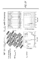
- FIG. 2A depicts computational results and illustration of one embodiment of the present invention.
- FIG. 2B depicts a plot of measured ( ⁇ E) 2 h ⁇ for doped KNbO 3 pellets, and for GaAs and CdTe (as used herein, h ⁇ means h times Greek nu or h-bar times Greek omega).
- FIG. 3 depicts TGA measurements of several embodiments of compounds of the present invention.
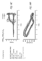
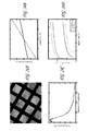
- FIG. 4 depicts dielectric response and hysteresis loops of compounds of the present invention.
- a and C are measured at 2 locations on the pellet. Same with B and D.
- A/C/E is the phase of piezoelectric response.
- B/D is the amplitude of piezoelectric response.
- E is like A and C, phase image. SEM of lamella is shown in inset.
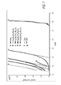
- FIG. 5 provides the light absorption properties of different compounds of the present invention using spectroscopic ellipsometry as well as for GaAs and CdTe.
- FIG. 6 depicts band gap versus dopant content in several embodiments of compounds of the present invention.
- FIG. 7 depicts photocurrent versus applied bias at various dopant levels of several devices of the present invention.
- FIG. 8 depicts X-ray diffraction patterns of embodiments of various compounds of the present invention.
- FIGS. 9A and 9B depict sample preparation, before reduction (light color) and after reduction (dark color).
- FIG. 10 depicts dielectric constant versus temperature at different frequencies for various compounds of the present invention.
- FIG. 11 depicts loss tangent versus temperature at different frequencies for various compounds of the present invention.
- FIG. 12 depicts a nanostructured solar cell comprising compounds of the present invention; interpenetrating networks of n- and p-type semi-conductors form a large-area heterojunction; a semiconducting FE absorber layer at the n-p interface enhances light absorption and carrier separation.
- FIGS. 13A-D depict various calculated properties of the KBNNO embodiment of the present invention.
- FIG. 14 High-vacuum PLD system possessing a 3-target manipulator (left rear).
- FIG. 15 depicts cross-section image demonstrating hetero-epitaxial LaAlO 3 on SrTiO 3 and coherency of atomic planes obtained by ALD of alternating binary oxides to demonstrate that high-quality interfaces can be obtained by this method. Also shown are Fourier-transform and converging beam electron diffraction pattern collected from the interfacial region.
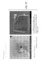
- FIGS. 17 A-G depict the preparation and surface characterization of KBNNO lamellae used in the experimental results described herein.
- FIGS. 18A-D depict phase and amplitude of piezoelectric hysteresis loops of KBNNO lamellae used in the experimental results described herein.
- FIG. 19 depicts a) Solar photon intensity versus wavelength, with the band gaps indicated for the classic semiconductors Si, CdTe, the FE perovskite BiFeO 3 and the new KBNNO materials. b) Results of X-Ray Diffraction (XRD) measurements for the KBNNO materials. As BNNO fraction increases, the peaks shift to higher lattice constant values. All XRD spectra do not show any evidence of secondary phase impurities.
- FIG. 20 depicts (KNbO 3 ) 8 ⁇ (BaNb 1/2 Ni 1/2 O 2.75 ) 4 solid solution crystal structures, with two structural motifs: Ni 2+ -V O —Ni 2+ (denoted as KBNNO-1) and Ni 2+ -V O —Nb 5+ (KBNNO-2). A cations and O atoms are omitted for clarity. Ni—O—Nb and Nb—O—Nb bonds are shown by solid black lines, while Ni—V O —Ni and Ni—V O —Ni are presented as dashed lines.
- FIG. 23 depicts band structures (top) and orbital-projected density of states (bottom) for KBNNO Ni—V O —Ni and Ni—V O —Nb solid solutions near the Fermi level.
- the high-symmetry points in the Brillouin zone are ⁇ (0, 0, 0), A ( ⁇ 0.5, 0.5, 0), B ( ⁇ 0.5, 0, 0), D ( ⁇ 0.5, 0, 0.5), E ( ⁇ 0.5, 0.5, 0.5), Z (0, 0, 0.5), C (0, 0.5, 0.5), Y (0, 0.5, 0).
- FIG. 24 depicts photocurrent measurements for the KBNNO samples.
- Solar cells convert sunlight to electricity cleanly and renewably, and can be implemented in geographically diverse areas, including off-grid.
- Crystalline silicon has long been the most widely used photovoltaic material, exhibiting cell efficiencies of 25%, but the cost of electricity from c-Si solar cells is approximately four times larger than that of electricity produced from fossil fuels.
- Thin film CdTe and CuIn x Ga 1-x Se 2 (CIGS) photovoltaics offer lower cost than c-Si but use rare, expensive, or toxic elements; CIGS also has problems with robustness and mass production.
- the dye-sensitized solar cell (DSSC), or Grätzel cell, has shown great promise, both in terms of high efficiency and low materials and embodied energy costs.
- the innovative architecture of the DSSC uses a mesostructured wide band gap semiconductor whose large surface area is sensitized with a molecular dye, and whose pores are infiltrated by an electrolyte. This architecture separates the functions of light absorption and electron and hole transport into three separate materials, and it ensures efficient charge separation by absorbing all photons precisely at the nanostructured interface.
- organometallic dye molecules corrosive I ⁇ /I 3 ⁇ redox couples, and volatile electrolytes has led to significant criticism that DSSCs are not robust enough for widespread deployment.
- BiFeO 3 Bulk and thin-film ferroelectric BiFeO 3 can be used as FE absorbers in photovoltaics, but current densities have been very low for two reasons. First, the band gap of BiFeO 3 is 2.5 eV, much larger than optimal for photovoltaics. Second, low mobilities inherent in FE oxides lead to short carrier collection lengths in planar cells. The incorporation of new FE oxide materials into a novel solar cell architecture can circumvent these two problems and yield a robust, inexpensive, and efficient solar cell.
- the present invention provides ferroelectric perovskites and compounds characterized as having a band gap, E gap , of less than 2.5 eV.
- Particularly suitable ferroelectric perovskites can also have band gap less than about 2.0 eV, or even from about 1.1 eV to about 1.6 eV.
- Suitable ferroelectric perovskites comprise a solid solution of KNbO 3 and BaNi 1/2 Nb 1/2 O 3- ⁇ , wherein ⁇ is in the range of from 0 to about 1.
- the solid solution of KNbO 3 and BaNi 1/2 Nb 1/2 O 3- ⁇ is represented as (1 ⁇ x)KNbO 3-x BaNi 1/2 Nb 1/2 O 3- ⁇ (KBNNO), wherein x is in the range of from about 0.01 to about 0.99.
- An equivalent representation of this formula is [KNbO 3 ] (1-x) [BaNi 1/2 Nb 1/2 O 3- ⁇ ] x .
- x is in the range of from about 0.1 to about 0.5, and is most preferably about 0.1.
- suitable ferroelectric perovskites can have 8 is in the range of from about 0.2 to about 0.3.
- Suitable ferroelectric perovskites will also be characterized as ferroelectric up to at least 100 degrees C., especially for use as materials in photovoltaic cells.
- the perovskite structure is readily characterized using X-ray diffraction.
- atomic substitution can be made.
- K atoms can be replaced by Na atoms in the structures described herein.
- Ni atoms can be replaced by Pd or Pt atoms.
- the present invention further provides for solid solutions of oxides comprising Ba, Nb, one or more of K and Na, and one or more of Ni, Pd and Pt.
- the solid solution of oxides, as more broadly described here are can also be characterized as being ferroelectric perovskites, which can be fabricated using the methods described herein to prepare photovoltaic devices and solar cells.
- Photovoltaic devices comprising one or more solar absorbing layers, wherein at least one of the solar absorbing layers comprises a semiconducting ferroelectric layer are also provided.
- the photovoltaic devices comprise a semiconducting ferroelectric layer that is characterized as having a band gap in the range of from about 1 to 2 eV.
- Certain preferred photovoltaic devices comprise a semiconducting ferroelectric layer being characterized as having a band gap in the range of from about 1.1 to 1.5 eV.
- the semiconducting ferroelectric layer can comprise a solid solution of KNbO 3 and BaNi 1/2 Nb 1/2 O 3- ⁇ , wherein ⁇ is typically in the range of from 0 to about 1.
- Suitable solid solutions of KNbO 3 and BaNi 1/2 Nb 1/2 O 3- ⁇ can be represented as (1 ⁇ x)KNbO 3-x BaNi 1/2 Nb 1/2 O 3- ⁇ (KBNNO), wherein x is in the range of from about 0.01 to about 0.99. In certain preferred embodiments x is in the range of from about 0.1 to about 0.5. In other embodiments, it is also preferred that 8 is in the range of from about 0.2 to about 0.3.
- Solar cells according to the present invention include a heterojunction of n- and p-type semiconductors.
- the heterjunction is characterized as comprising an interface layer disposed between the n- and p-type semiconductors, the interface layer comprising a semiconducting ferroelectric absorber layer capable of enhancing light absorption and carrier separation.
- Suitable heterojunctions of n- and p-type semiconductors can be further characterized as being nanostructured, such as described further herein and in the examples below
- Suitable solar cells will typically include a back contact in electrical communication with the p-type semiconductor, a blocking layer in electrical communication with the n-type semiconductor, and a front contact in electrical communication with the blocking layer. Accordingly, light radiation incident upon the front contact gives rise to an electric load between the back contact and the front contact.
- the present invention also provides a heterojunction comprising materials that provide a Type II interface, i.e. that which has band offsets that provide a potential landscape to separate carriers.
- Suitable Type II interfaces include, for example, a bi-polar n-p junction, a solar cell comprising a heterojunction consisting of n+-n, p-p+, or other combinations of materials.
- the present invention also encompasses bi-polar homojunctions, typically characterized by an abrupt or gradual gradient in composition of the complex oxide ferroelectric within the solar cell achieving doping provides the same result without additional materials.
- the solar cells described herein can have a ferroelectric absorber layer comprising a perovskite material.
- Suitable perovskite materials may include a semiconducting ferroelectric layer, one example being a solid solution of KNbO 3 and BaNi 1/2 Nb 1/2 O 3- ⁇ , wherein ⁇ is in the range of from 0 to about 1.
- ⁇ can be in the range of from about 0.2 to about 0.3.
- the available band gaps span the 1.1-1.5 eV range that is optimal for high-efficiency single junction solar cells.
- the KBNNO materials can increase efficiency relative to BiFeO 3 , by enabling conversion of green/yellow/red/near-IR photons in addition to blue.
- the polar character of the FE oxide also enables mechanisms of charge separation that are entirely different from those in solar cells based on p-n junctions. 2
- oxides are robust with respect to changes in environment, their elemental abundances enable inexpensive cells, and modern oxide growth techniques pave the way for scalable integration of components. Therefore, the proposed oxide-based solar cells have the potential to be cheaper than c-Si solar cells and much more robust than DSSC or organic solar cells.
- the ETA cell structure consists of a high surface area, mesoporous n-type semiconductor coated with a thin ( ⁇ 20 nm) absorber layer, with interstices filled with a p-type semiconductor to create an interpenetrating hetero-junction, as shown in FIG. 12 .
- Light is absorbed by the absorber layer, generating an electron and hole that must be separated laterally across the n- and p-type interfaces, respectively, without recombining in the bulk material.
- Poled FE absorbers are expected to enhance charge separation and photovoltage compared to typical semiconductors. After separation, charges must be transported in the n- and p-type layers to opposite contacts, without recombining interfacially, in order to produce electrical current. The polarization of the FE absorber may even eliminate the need for p- and n-type contacts altogether, if ohmic contacts can be made to metals or transparent conductors.
- Density functional theory (DFT) calculations of the electronic structure of KBNNO ( FIG. 13 ABO 3 picture and DFT band structure) indicated that the response of KNbO 3 to the incorporation of Ni 2+ and vacancies was similar to that predicted for PbTiO 3 .
- DFT Density functional theory
- the architecture of this cell consists of an array of n-type oxide nanowires (e.g. ZnO or ABO 3 ), coated with an extremely thin ( ⁇ 10 nm) absorber (ETA) layer of KBNNO semiconducting FE oxide or other low-band gap FE oxide, and filled by a wide band gap hole conductor.
- n-type oxide nanowires e
- FE oxides for light absorption and charge separation are the central new feature of this design. Without being bound by any limiting theory, we believe that semiconducting FE oxides can play an increasingly significant role in solar energy harvesting, charge separation, and energy transfer due to their low cost and ability to separate electrons and holes efficiently. While FE oxides have been considered and investigated for photocatalysis and photovoltaics, their large band gaps and low electronic carrier mobilities have limited their applicability. Furthermore, the prevailing view has been that the depolarizing field of FEs would limit their application in nanoscale devices, since reduction of the FE thickness below ⁇ 100 nm is typically accompanied by a dramatic reduction of the FE polarization.
- the nanostructured interface where light is absorbed and charges are separated in the DSSC design can be replaced by one or more thin conformal coatings of high-quality, semiconducting FE oxide.
- Unique and technologically relevant features of the semiconducting FE can be leveraged to absorb visible light, facilitate charge separation and reduce interfacial recombination within a single material.
- KBNNO can be used as the absorber material, we can adjust the absorber composition as need be to achieve more scalable synthesis, higher quality interfaces and greater carrier mobility.
- the design of the new all or nearly all-oxide cell materials and configurations is supported by proximal probe, mesoscopic, and ensemble characterizations as discussed below.
- FE oxide coatings increases solar cell efficiency compared to DSSCs and other nanostructured solar cells while maintaining low fabrication costs. Materials are earth abundant and can be processed under relatively benign conditions.
- FE Absorber Thin Films The selection of a chemically-designed semiconducting FE oxide layer and its incorporation in nanostructured solar cells satisfies a number of requirements in addition to having a band gap in the visible and a configuration that can orient the FE polarization.
- the deposition process is capable of producing materials with precise chemical control, thickness, and even surface chemical termination.
- the processing results in high-quality material interfaces (ideally epitaxial) with conformal coatings on n-type ZnO nanowires or alternately, TiO 2 or ABO 3 nanostructures.
- Thin-film deposition processes can be rapidly optimized and adapted to producing conformal, ultra-thin coatings on arrayed and porous nanostructures.
- PLD pulsed laser deposition
- ALD atomic layer deposition
- PLD can be used to obtain heteroepitaxial complex oxide growth on binary oxide (MgO) nanowires.
- MgO binary oxide
- PLD is considered to be of limited scalability for high-volume, low-cost production.
- ALD is an effective method for producing highly conformal binary oxides, other inorganic materials, and FE and related oxide perovskite films in planar form (e.g. PbTiO 3 , Pb(Zr 1-x Ti x )O 3 , SrTiO 3 ), with the potential for high scalability.
- KBNNO thin films can be grown at several compositions.
- the absorber composition may, in some embodiments, be modified such as by including semiconducting FE oxides.
- Planar semiconducting FE oxide perovskite films can be deposited on conducting perovskite and binary oxide substrates via PLD from bulk targets using solid-state chemical routes.
- ALD processes can be used for depositing KNO and KBNNO planar films via ALD using metallorganic precursors.
- PLD is one of the most common methods of obtaining complex oxide perovskite thin films of high quality, including KNO.
- Translation of the bulk synthesis of KBNNO from pellet form to a thin film process presents significant challenges.
- Systematic careful variations of the base vacuum and oxygen partial pressure, the substrate temperature, and the laser fluence/pulse energy can be used to obtain the target oxygen stoichiometry of the KBNNO phase, especially considering the multi-valent state of Ni 2+ and Ni 3+ that has been observed in recent XPS characterizations of the bulk KBNNO material.
- conditions can be optimized to permit heteroepitaxial growth of KBNNO on conductive perovskite oxide and other oxide substrates, permitting optical and scanned-probe characterization of these interfaces to assess suitability for solar cell prototype devices.
- ALD of perovskite oxides is far less common and more challenging than ALD of metals or binary oxides, since it typically involves either a metalorganic precursor with multiple metals or the sequential deposition of multiple single-metal metalorganic precursors, resulting in the deposition of an amorphous film that requires subsequent annealing in oxygen.
- Precursor selection for use in an ALD temperature window is complicated by the dearth of high-volatility metalorganic precursors.
- heteroepitaxial LaAlO 3 films possessing atomic planes coherent with substrate SrTiO 3 can be obtained via ALD of amorphous and alternating bilayers of La 2 O 3 and Al 2 O 3 films using tris(isopropylcyclopentadienyl)lanthanum and trimethyl aluminum onto TiO 2 -terminated SrTiO 3 and subsequent annealing ( FIG. 15 ).
- Optimization of pre- and post-anneal stoichiometry with the aid of Rutherford backscattering spectroscopy and X-ray fluorescence can be used to achieve the desired composition.
- a high-vacuum PLD system is constructed or provided, which system includes an excimer laser (KrF, 248 nm) configured for depositing complex perovskite oxides from single targets.
- the system also includes three-target automatically-indexed manipulator capabilities for sequenced deposition of other materials, including conductive perovskites (e.g. SrRuO 3 , Nb:STO) ZnO ( FIG. 15 ).
- conductive perovskites e.g. SrRuO 3 , Nb:STO
- Other configurations can also be achieved using other excimer wavelengths, or Nd:YAG or other lasers capable of pulsed UV radiation and ablation.
- the target manipulator need not be a three-target indexed one, but the system typically includes capability for deposition in a reactive environment to enable optimization of O stoichiometry.
- a commercial research-scale ALD reactor system is modified to include a liquid injection subsystem enabling a wide range of lower-volatility metalorganics for investigating candidate ALD precursors for obtaining the targeted complex oxide thin films, including BiFeO 3 .
- ALD is not selected for its rapid growth rate, this liquid injection precursor delivery method can be considerably faster than waiting for the evaporation, or even N 2 -assisted evaporation, of low vapor-pressure precursors.
- the two proposed thin-film deposition approaches for obtaining complex oxide films and coatings are complementary. Since the starting material for PLD is the stoichiometrically correct pellet, we expect to be able to produce the desired KBNNO phase as an epitaxial film, through systematically-controlled variation of deposition parameters, post-deposition in situ or ex situ annealing (if necessary), and structural characterization. PLD also permits growth of other semiconducting FE complex oxide perovskite phases on conducting and oxide substrates with control of thickness, grain size, and orientation.
- Multi-Component Oxide Layers In addition to evaluation of deposited film uniformity and adhesion using scanning probes and scanning electron microscopy, the interfacial quality, e.g. the nature and concentration of defects that can act as trap states, microstructure, and crystallographic structure, can require characterization using high-resolution TEM and electron diffraction. Thin film products can also be analyzed using X-ray diffraction and compositional analysis using X-ray fluorescence and Rutherford backscattering.
- Optical reflectivity, absorption, and spectroscopic ellipsometry of the deposited thin-film semiconducting FE oxide perovskites can be collected and analyzed to validate model calculations of dielectric function and electronic density of states.
- electronic transport measurements in electrically-contacted films can be performed to evaluate carrier concentrations and Hall mobilities.
- ABO 3 nanostructures are prepared and used for proximal probing to evaluate their local FE properties, including co-axial nanostructures comprised of semiconducting cores and FE ABO 3 shells, similar to the nanostructures proposed herein.
- Electron beam induced current (EBIC) and scanned photocurrent can also be used to evaluate the local electronic landscape within intrinsic semiconducting nanowires with blocking contacts.
- Such local probes of films and nanostructures can be used to evaluate band bending, carrier recombination and diffusion lengths, and local polar character; these are increasingly important and common methods for spatially-resolved quality control of the absorber(s), the n-type and p-type conductors, and their interfaces.
- Characterization of the FE polarization, coercive field and phase transition temperature can be carried out on thin films obtained by PLD and ALD.
- Local FE switching and hysteresis can be collected using a scanning probe microscope to measure coercive fields, and capacitance-voltage measurements can be used to quantify FE polarization. These measurements can be carried out both in the dark and under illumination by a scanning monochromatized supercontinuum source, to investigate the effect of local orientation of polarization and illumination wavelength on photocurrent.
- Individual co-axial cylindrical nanowires composed of ZnO cores and KBNNO and other material shells can be contacted electrically, with one contact placed on the core (following selective etching) and the other on the shell.
- Terahertz spectroscopy and UV/visible transient absorption (TA) spectroscopies can be used to probe dynamics of photoexcited carriers and carrier mobility. Carrier lifetimes and mobilities are the primary determining factors in the carrier collection length, which determines the optimal thickness of the absorber coating. Temperature dependent time-resolved terahertz spectroscopy (TRTS) and TA spectroscopy is performed using an ultrafast laser system. THz time domain spectroscopy (THz-TDS) is a powerful technique to probe conductivity in conventional semiconductors, because carriers typically have scattering rates on the order of 10 12 -10 14 s ⁇ 1 , enabling detailed modeling.
- TRTS probes the transient far-IR response after photoexcitation with a UV/visible/mid-IR pump pulse, with sub-picosecond time resolution.
- TRTS can be applied to measure the carrier dynamics in bulk ZnO as well as ZnO thin films and nanostructures. Temperature-dependent studies have been used to reveal donor densities and activation energies, and photoexcited carrier lifetimes and mobilities can be measured as a function of microstructure and morphology. The non-contact measurement of electrical properties is particularly appealing for new materials being developed here because there is no need to search for new schemes to make ohmic contacts, as would be the case with standard electrical measurements. While photon flux is much higher in these pulsed experiments than in actual solar irradiation, the measurements provide useful insight and define limiting performance in high-flux conditions.
- UV/vis TA is an excellent complement to TRTS, because TA measures interband dynamics with sub-100 femtosecond resolution using a broadband UV/vis probe after photoexcitation by a tunable pump pulse.
- THz spectroscopy and TA have rarely been applied to investigate complex oxides.
- terahertz spectroscopy has been used to probe low-energy excitations in charge-ordered manganites, polaronic conduction in SrTiO 3 , and polarization dynamics in ferroelectric BiFeO 3 .
- TA has been used to investigate photoinduced charge and spin dynamics as well as charge transfer for photocatalytic water splitting.
- TRTS and TA to probe photoexcited carrier lifetimes, mobilities, and ultrafast interfacial charge transfer in semiconducting FE remains an unexplored and promising field.
- the range of stable semiconducting polar absorbers can be expanded by exploring the incorporation of Ba(Ni 1/2 Nb 1/2 )O 2.75 into (Na,K)NbO 3 solid solutions that have shown enhanced ferroelectric activity. We can also probe the effect of the redox chemistry of Ni 2+ on the FE polarization and the band gap. Thermogravimetric analyses (TGA) and measurements using XPS indicate that as-prepared samples of KBNNO contain oxygen vacancies with Ni in the 2+ state.
- Bi 5+ -substituted systems such as BaBiO 3 -PT and K(Nb,Bi)O 3 also yield semi-conducting FEs with gaps in the optical range.
- Davies has attempted to synthesize bulk samples of BaBiO 3 -PT; these experiments, however, yielded two-phase mixtures of BaBiO 3 and PT.
- Members of this family that can be prepared using standard ceramic methods, i.e. where Bi 5+ is stable (in air) at ⁇ 1100° C., are restricted to examples where the B 3+ counter-ion is a large cation such as La 3+ , Nd 3+ or In 3+ .
- the cell volumes in those systems are still too large to permit significant mixing in ferroelectric end-members such as PT or even KNO. To facilitate mixing, it is critical to reduce the mismatch by maximizing the volume of the FE end-member, while minimizing the volume of the Bi 5+ component.
- first-principles DFT and thermodynamic modeling To provide guidance for the development of the new FE absorber materials and for the experimental fabrication of the interfaces, we can use first-principles DFT and thermodynamic modeling. Theoretically predicting the rich variety of reconstructions found for perovskite surfaces is possible. This theory can also show how synthesis and annealing pathways can be modified to create off-stoichiometry surfaces with a desired composition and structure. Surface composition and structure is highly sensitive to the polarization of the oxide. A first-principles methodology can be used for calculating the photocurrent generated by the bulk photovoltaic effect. Comparison of the calculated and the observed photocurrent for single crystal BaTiO3 shows that BPVE is the main mechanism for the separation of photoexcited carriers by the bulk of a single-crystal polar material.
- thermodynamically favorable composition and structure at the interface under various synthesis conditions.
- the redox chemistry of the Ni cation can be important, as it is possible that the interactions at the interface can change the oxidation state of Ni and the band gap.
- we can also perform calculations for structures where point defects e.g.
- Low band-gap FE materials based on Ni 2+ and Bi 5+ substitution can also be fabricated.
- Bi 5+ substitution work we have identified several promising candidate compositions (e.g. PIN-BIB) as outlined above. For these, our main task can be to calculate electronic properties, to determine whether good FE behavior and a low band gap are in fact expected for the proposed compositions, thus narrowing down the list of possible candidate solutions. Additionally, we can examine compositional replacement of Sc ions in the B-site due to the high cost of Sc metal. Here, the most promising strategy is to use a combination of a +2 and a +4 cations with the same or larger average size as the Sc 3+ (e.g. Mg 2+ and Zr 4+ , or Cd 2+ and Zr 4+ , or Mg 2+ and Tb 4+ ).
- Solar cells can be fabricated to incorporate semiconducting FEs as the absorber and charge separation material. Simplified versions of the solar cell are first tested to select materials and interfaces. For example, planar cells based on epitaxial FE films are tested to measure light absorption and charge collection for the case of ideal, defect-free interfaces. Conflicting constraints requiring thicker films for light harvesting and thinner films for charge collection can likely dictate the use of nanostructured ETA architectures to achieve high efficiency.
- the solar cells may also, but not necessarily, include p- and n-type contacts.
- the p-n junction creates the electric field to separate electrons and holes.
- poled FE have a permanent polarization that can drive electrons and holes to opposite contacts (via the BPVE) without the need for the built-in field of a p-n junction.
- Photovoltaics based on FE BiFeO 3 with symmetric metal contacts have been demonstrated.
- One metal and one transparent conducting oxide contact may provide a good quality device. Finding ohmic contacts to KBNNO with appropriate work functions and high quality interfaces can be a key challenge to such a design.
- p- and n-type layers may not be strictly necessary for charge separation, they could add significant versatility and flexibility to the design.
- thin films of p- and n-type layers could serve as buffers between the FE and the conductive contacts to reduce the number of constraints on any single material or interface.
- a FE ETA cell can use all perovskite materials for exceptional interfacial fidelity, with highly conductive n- and p-type materials and a FE absorber.
- the nanowire array can be either n-type or p-type, depending on synthesis capabilities, with the pore-filling material taking on the opposite function.
- FE processing temperatures can be too high for typical transparent conducting oxide films such as ITO, so two options can be considered.
- Transparent conductive perovskites such as Nb:SrTiO 3 can be used in a superstrate configuration, or metal-coated glass or metal foils with perovskite film buffer layer can be used in the substrate configuration with ITO or AZO deposited after FE processing is completed.
- a suitable architecture can be provided using n- or p-type nanowires, lattice-match materials, and by the band positions and work functions of available materials.
- the band diagram can take on a staircase-like structure with type II band offsets, to facilitate interfacial charge transfer in the desired direction while blocking the opposite charge from moving in that direction.
- ZnO nanowire arrays can initially be used as the n-type material. These can be used for ETA cells with chalcogenide absorbers and also for DSSCs. However, the ZnO/absorber interface is likely to be highly defective.
- ALD ALD of a very thin ( ⁇ 1-3 nm) buffer layer to passivate defects while allowing tunneling of carriers. Similar strategies have been successful in DSSCs.
- Suitable buffer layers may include Al 2 O 3 or TiO 2 . The effect of non-epitaxial interfaces on the FE character of the thin absorber compared to an epitaxial perovskite interface using both solar cell and ex situ materials characterization is investigated.
- Liquid electrolytes can be used as the hole conductor in the early investigative stages, to facilitate good contacts with a tunable redox potential, although stability of the FE in electrolyte can have to be monitored.
- Solid state p-type materials are selected that have appropriate band offsets to accept holes from the absorber while blocking electrons.
- optimal absorber thickness is determined via charge separation and bulk recombination.
- the charge collection length of the FE absorber, with and without polarization, is determined using a combination of planar solar cells of varying thickness and ex situ materials measurements. If the collection length is much smaller than the optical absorption depth, then nanostructured ETA configurations can be required to improve light harvesting.
- the thickness of the FE coating on the nanostructured electrode can be as large as possible to minimize interfacial area while still enabling efficient charge separation. Based on the optimal thickness, the nanowire length, diameter, and pitch can be designed to provide the interfacial area necessary to harvest nearly all visible light, as well as appropriate pathways for electron and hole collection.
- AMPS Microelectronic and Photonic Structures
- AMPS requires data such as absorption spectra and density of states of each layer as input, and it then calculates the expected band structure, electric field distribution, and photovoltaic response by solving Poisson's equation and the continuity equations. While AMPS can provide some guidance, it is limited to 1D and does not explicitly account for the BPVE of our FE absorbers. Therefore, modifications to AMPS or home-grown code can also be used.
- Working solar cells are tested using I-V characterization and wavelength-dependent light harvesting and quantum efficiency measurements, as well as intensity-modulated photocurrent and photovoltage spectroscopy, impedance spectroscopy, and current and voltage decay measurements. These techniques can be used to determine limitations in power conversion efficiencies and to investigate fundamental aspects of charge transport and recombination in DSSCs, organic solar cells, and chalcogenide-based ETA cells.
- the combination of solar cell studies with characterization of nanowires and thin films of functional oxide-based structures can provide valuable feedback for materials selection, processing, and architecture design and can enable optimization of a robust lab-scale solar cell.
- IQE interfacial recombination during charge transport or bulk recombination during charge separation that limits overall efficiency.
- IQE that is independent of nanowire length indicates a charge separation-limited regime, while IQE that decreases with increasing nanowire length indicates transport-limited.
- Light harvesting efficiency (LHE) measurements can indicate whether the absorber volume is large enough to harvest all incident light. If absorbance is low, absorber thickness should be increased if IQE is transport-limited but nanowire surface area should be increased if IQE is charge separation-limited. Surface area can be increased by increasing either the length or the number density of the nanowires.
- the oxide-based solar cells described herein have the potential to be cheaper than crystalline silicon solar cells and much more robust than DSSC or organic solar cells.
- the new thin film solar cells can therefore offer the prospect of competing with conventional non-renewable electricity production from coal or oil.
- Market volumes for thin film solar cells are already in the multibillion dollar range and are expected to grow strongly in the future.
- a more widespread use of solar energy can also reduce CO 2 emissions.
- Availability of efficient, low-cost, clean, and sustainable solar cells made from earth-abundant, non-toxic materials would transform the US and global energy portfolio.
- the work carried out according to this specification can be used to develop novel polar semiconductor oxide compositions, new thin film and nanoheterostructure fabrication methods, and can enrich the understanding of how the epitaxial interfaces affect carrier transport from the absorber to the electrode.
- Design, synthesis, and characterization of new FE oxides with band gaps in the range of 1-2 eV can enable many new applications in optoelectronics as well as photovoltaics.
- New mechanisms of charge separation elicited by the poled FE absorber without the need for a p-n junction could lead to a new paradigm in solar cell design.
- the semiconductor ferroelectric is desirably thermodynamically stable and able to be fabricated by an inexpensive, scalable route.
- solid solutions of KNbO 3 (KNO) and BaNi 1/2 Nb 1/2 O 3- ⁇ can be synthesized using solid state conventional methods, are polar at room temperature and exhibit direct band gaps in the 1.1-1.6 eV range. Accordingly, these materials are suitable for utilizing the visual part of the solar spectrum and can be used in thin film photovoltaic devices.
- the pellets were then placed on Pt foil in a covered alumina crucible, surrounded by sacrificial powder of the same composition, and sintered at temperatures between 1050-1250° C., depending on the composition.
- KNbO 3 melts at ⁇ 1050° C. and is sintered at a lower temperature
- K 0.5 Ba 0.5 Ni 0.25 Nb 0.75 O 3- ⁇ is sintered above 1200° C. to achieve >90% theoretical density.
- Water absorption is known to be a problem with KNbO 3 .
- at all stages of synthesis samples are either kept at elevated temperature (at least 200° C.) or in a dessicator, and exposure to moisture is kept to a minimum.
- KNbO 3 has an orthorhombic distortion from cubic symmetry at room temperature that can be clearly seen in the peak splittings of a powder X-ray diffraction (PXRD) pattern.
- 10% doping of BaNi 0.5 Nb 0.5 O 3- ⁇ results in a pattern that appears cubic to the resolution of our laboratory X-ray diffractometer (XRD).
- XRD X-ray diffractometer
- the oxygen content in the solid solution of this perovskite can vary from between 3 if all the Nickel is 3+, down to 3 ⁇ (x/4), if all the Nickel is 2+.
- un-sintered pellets appear yellow in color.
- the pellets turn to a blackish gray, indicating some level of reduction and accompanying oxygen loss.
- FIGS. 9A and 9B Quantification of this oxygen loss should be possible by thermogravimetric analysis (TGA) and should give an idea of the oxidation state of the Nickel.
- TGA thermogravimetric analysis
- the XRD patterns of these reduced samples show a slightly increased background, but also show the same single phase pattern with a nearly identical lattice parameter. Further annealing in an oxygen atmosphere can result in a re-oxidation of the material.
- Frequency dependent dielectric constant measurements have been performed on the 10, 20, 30 and 40% doped samples.
- Pure KNbO 3 shows a series of anomalies in its dielectric constant v. Temperature curves which correspond to the 3 structural transitions at ⁇ 10, 225 and 435° C. In the 10% doped material, an anomaly is visible at 345° C., which may indicate a tetragonal to cubic structural transition, and may correspond to the 435° C. transition in pure KNbO 3 . No anomaly is visible above room temperature in materials with doping levels greater than 10%. The materials become more lossy with increased doping of conductive Ni cations.
- Characterization and analysis of the optical properties were carried out using variable angle spectroscopic ellipsometry (SE), and proximal probing (local ferroelectric piezoelectric switching and piezoresponse force microscopy) of the as-prepared pellet samples and of Ga+ milled lamella cross-section specimens extracted from the pellet using a focused ion beam (FIB) tool.
- SE variable angle spectroscopic ellipsometry
- proximal probing local ferroelectric piezoelectric switching and piezoresponse force microscopy
- Variable-angle SE analysis was performed (247 nm ⁇ 1 ⁇ m) using a model M2000 (J. A. Woollam), using Glan-Taylor polarizers, a rotating compensator, and deuterium and quartz tungsten halogen lamps. Ellipsometric parameters ⁇ and ⁇ , defined via
- the direct and indirect optical band gaps can be estimated by extrapolating the straight line portions of the ( ⁇ E) 2 vs. hw and ⁇ 1/2 vs. hw, respectively, where hw is the incident photon energy in units of eV and ⁇ is the absorption coefficient (expressed in units of cm ⁇ 1 .) that can be calculated as
- FIG. 2B Shown in FIG. 2B is a plot of ( ⁇ E) 2 hw for doped KNbO 3 pellets, and for GaAs and CdTe.
- the (1 ⁇ x)KNbO 3-x BaNi 1/2 Nb 1/2 O 3- ⁇ (KBNNO) system was chosen to optimize the stability of Ni +2 -oxygen vacancy combination while preserving polarization.
- Potassium niobate has a high transition temperature (705 K) and polarization (0.6 C/m 2 at 0 K), driven by the off-center distortion of Nb ions.
- Nb ions are often found in five-fold coordination environment in oxides, and Nb-containing ferroelectric perovskites tolerate a high concentration of vacancies. Accordingly, without being limited to any theory of operation, Nb-containing ferroelectric perovskites are believed to be able to accommodate the Ni +2 -oxygen vacancy combination.
- Ba was chosen as the A-site substitutent as it has the same ionic size as K, promoting solubility.
- the large size of the K and Ba cations can also favor vacancy formation, as Ni 3+ is too small and is stable in a perovskites with La 3+ on the A-site, whereas Ni 2+ is stable in ferroelectric (“FE”) ABO 3 such as PbNi 1/3 Nb 2/3 O 3 .
- X-ray diffraction (XRD) results show that the structure is perovskite for all solutions with no impurity peaks.
- the increase in lattice parameters with BNN substitution (Table I) is consistent with the presence of the Ni 2+ cation with large ionic size (0.68 ⁇ ) than for Nb 5+ (0.64 ⁇ ) or Ni 3+ (0.60 ⁇ ).
- FIG. 5 We find that the band gaps are small, in the 1.1-1.6 eV range, a dramatic 2 eV drop from the >3.2 eV band gap of the parent KNbO 3 material.
- FIG. 6 Table I
- compositional band gap changes are believed to be due to the interplay between local bonding and the band gap in KBNNO as elucidated by DFT calculations.
- Our calculations show that while both configurations result in a low band gap, the E gap value for Ni—Nb configuration is lower than for the Ni—Ni configuration.
- Ni concentration increases more Ni-vac-Ni are formed, as Ni-vac-Ni is more energetically favorable, and therefore the measured, average E gap rises.
- An alternative explanation is that as BNN content increases, the larger size of the Ni 2+ leads to a decrease of tolerance factor and an increased magnitude of octahedral rotations.
- KNO-BNNO solid solution can be synthesized by conventional solid state routes, and exhibit stable room temperature ferroelectricity, and a low, direct band gap comparable to that of the Si and CdTe semiconductors used in current photovoltaic applications. Due to the lower band gap, these materials exhibit photocurrents an order of magnitude larger than previously measured for bulk ferroelectric perovskite materials.
- the wide band gap of typical FE perovskites is due to the fundamental bonding characteristics of ABO 3 materials.
- the excitation across the band gap is essentially a charge transfer from the O 2p states at the valence band maximum (VBM) to the transition metal d states at the conduction band minimum (CBM). Due to a large electronegativity difference between the oxygen and transition metal atoms, the band gap is quite large (3-5 eV). However, it is the presence of the transition metal cations in the O6 cage that gives rise to ferroelectricity.
- VBM valence band maximum
- CBM conduction band minimum
- BFO the subject of a number of investigations for photovoltaic applications, with promising results.
- BFO is capable of absorbing only 20% of the solar spectrum.
- a new approach is necessary to circumvent the fundamental band-gap related limitation on the solar energy conversion efficiency in FE perovskites.
- two different transition metal cations on the perovskite B-site are used to create FE perovskites with low band gaps, with one cation driving ferroelectricity and the other giving an Eg in the visual range.
- Ferroelectric perovskite KNbO 3 (KNO) is used to provide off-center distortions and polarization, and this KNO is mixed with BaNi 1/2 Nb 1/2 O 3- ⁇ (BNNO) to introduce a combination of Ni 2+ on the B-site and an oxygen vacancy, which can give rise to electronic states in the gap of the parent KNO material.
- Nb ions are often found in five-fold coordination environments in oxides, and Nb-containing FE perovskites can tolerate a high concentration of vacancies. Therefore, B-site Nb ions should be able to accommodate the Ni 2+ -oxygen vacancy combination.
- Ba was chosen as the A-site substituent, as it has the same ionic radius as K, promoting solubility.
- Ni 3+ has a small ionic radius and is only stable in perovskites with (small) La 3+ cations on the A-site, whereas the larger Ni 2+ ion is known to be stable in FE compounds such as PbNi 1/3 Nb 2/3 O 3 .
- the calculated P is 0.19 C/m 2 and 0.18 C/m 2 for the two KBNNO structures, mainly due to the off-center distortions of the Nb cations.
- DFT+U free energy calculations find oxygen vacancies to be thermodynamically favored, indicating that the material is in the KBNNO state.
- KBNNO samples are not conductive, in contrast to the KBNNO ox , for which the DFT+U calculations predict a metallic state. Therefore, the synthesized material is indeed KBNNO, with oxygen vacancies.
- the light absorption properties of the KBNNO materials were characterized using spectroscopic ellipsometry ( FIG. 22 a ).
- the KBNNO band gaps were found to be in the 1.1-1.6 eV range; this is dramatically lower than the 3.2 eV band gap of the KNO material ( FIG. 22 b ). Due to the smaller band gap, the samples are all blue-green, in contrast to KNO which is white.
- the VBM consists of hybridized Ni 3d and O 2p states, while the CBM is composed of Nb 4d states. Comparison to KNO shows that the filled Ni 3d gap states in KBNNO play a crucial role in lowering the band gap.
- compositional band gap changes are due to the interplay between local bonding and the band gap in KBNNO, as elucidated by LDA+U calculations. It is believed that there are two possible configurations for the oxygen vacancies in KBNNO, Ni—VO—Ni and Ni—VO—Nb. Calculations show that while both configurations result in a lower band gap due the introduction of the Ni 3d states, an extra density of states peak, contributed by the d-orbitals of the six-fold coordinated Ni is present in the VBM in Ni—VO—Nb. ( FIG. 23 ) Therefore the Eg of Ni—VO—Nb configuration is lower than that of the Ni—VO—Ni. This configuration is also calculated to be more energetically favorable. At low BNNO concentration, the Ni cations are isolated, so the Ni—VO—Nb arrangement is prevalent. As Ni concentration increases, more Ni—VO—Ni are formed and therefore the measured Eg rises.
- KBNNO shows superior photoresponse properties ( FIG. 24 d ).
- the measured current is two orders of magnitude larger for KBNNO than for BTO.
- the favorable band gap and transport properties of KBNNO eliminate the chief obstacles for the use of FE oxides in solar energy conversion devices.
- KBNNO solid solutions have been synthesized by a solid-state route.
- KBNNO solid solutions exhibit stable room-temperature ferroelectricity, and a low, direct band gap comparable to that of the Si and CdTe semiconductors used in current photovoltaic applications.
- the KBNNO material also exhibits photocurrents two orders of magnitude larger than those of classic bulk FE perovskite materials.
- the pellets were placed on Pt foil in a covered alumina crucible, surrounded by sacrificial powder of the same composition, and sintered at temperatures between 1050-1250° C., depending on the composition.
- a covered alumina crucible surrounded by sacrificial powder of the same composition, and sintered at temperatures between 1050-1250° C., depending on the composition.
- H 2 O which is an issue in the synthesis of KNbO 3
- at all stages of the synthesis samples were either kept at elevated temperature (at least 200° C.) or in a dessicator to minimize their exposure to moisture.
- Powder x-ray diffraction (XRD) patterns of the samples were collected on a laboratory x-ray diffractometer (Rigaku GiegerFlex D/Max-B) using Cu K radiation generated at 45 kV and 30 mA.
- the dielectric data were collected on pellets coated with Ag paint (Heraeus ST1601-14 type) to provide electrical contacts for the Pt lead wires.
- the dielectric properties were investigated as a function of frequency and temperature using a high-precision impedance-capacitance-resistance meter (Hewlett-Packard Model 4284A) and a high temperature thermal chamber. The sample temperature was monitored by an S-type thermocouple positioned near the pellet.
- Spectroscopic ellipsometry was performed in the wavelength range 247-1000 nm using a variable-angle spectroscopic ellipsometer equipped with Glan-Taylor polarizers, a rotating compensator, and deuterium and quartz halogen lamps for spectral coverage (J. A. Woollam Co. Inc., Model M2000). Measurement of the components of linearly polarized reflectivity at each selected wavelength were used to obtain ellipsometric parameters ⁇ and ⁇ through the relation tan
- An integrated focused ion beam and scanning electron microscope (FEI Company DB235) equipped with a lift-out tool (Omniprobe) was used to extract thin-film lamellae from the bulk synthesized KBNNO. Briefly, a thin layer of carbon by sputtering coating (several tens of nm) is first deposited to provide protection against subsequent ion-beam irradiation and to enhance the imaging contrast. This was followed by deposition of a 500-nm thick platinum film using ion beam-assisted deposition onto the lift-out area, preventing direct ion-beam damage during the process.
- the lift-out preparation process consists of initial cross-sectional milling steps on both sides, a series of thinning steps using lower ion-beam currents, a finer-scale cross-sectional cleaning using ⁇ 100 pA ion-beam current, and ion-beam local deposition of Pt to affix the lamella to the lift-out tool.
- a low beam current ( ⁇ 100 pA) was maintained during the final release of the lamella from the substrate.
- each harvested lamella was transferred carefully to glass substrates coated with layers of fluorinated tin oxide (TEC-15 supplied by Ted Pella) and a top coating of 30 nm of In (selected to facilitate wetting of the bottom contact to the lamella) deposited via electron-beam evaporation in vacuum (BOC Edwards model A306).
- TEC-15 fluorinated tin oxide
- In selected to facilitate wetting of the bottom contact to the lamella
- BOC Edwards model A306 electron-beam evaporation in vacuum
- Ferroelectric switching within the lamellae was evaluated using local piezoresponse using a scanning probe microscope (Asylum Research MFP-3D) and Pt-coated Si probes (AC 240TM, Olympus, nominal stiffness constant ⁇ 2 N/m).
- a triangular waveform (frequency 0.025 Hz, peak-to-peak bias of 10 V) was applied to the bottom electrode while a sinusoidal AC probing voltage (5 kHz, 0.5 V amplitude) was applied to the cantilever tip to collect the variation in the cantilever phase as a function of the bias voltage.
- the cantilever phase signal at the modulation frequency was collected with the aid of a digital lock-in amplifier (Stanford Research Systems SR830).
- LDA+U is unable to predict Eg with the accuracy of the more advanced hybrid functionals or GW methods, it can still provide a good description of the change of Eg with respect to the solid solution cation ordering.
- a simplified version of the rotationally invariant formulation of the LDA+U method was employed, where U can be determined by self-consistent linear response calculations.
Abstract
Description
are extracted from direct measurements of Rp and Rs, the reflection coefficients for light polarization parallel (p), and perpendicular (s) to the plane of incidence. The wavelength-dependent complex index of refraction is obtained for each sample by assuming a model of a semi-infinite half space of the material surrounded by vacuum, and assuming an optically isotropic medium (∈11=∈22=∈33 and ∈12=∈13, with ∈ij=ji, with i, j=1, 2, 3. The real and imaginary components of the complex dielectric function (or optical index of refraction) are calculated via Maxwell's equations.
with k the extinction coefficient. Shown in
| TABLE I |
| Variation of direct gap with composition. |
| Composition | Direct Egap (eV) | ||
| KNbO3 | 3.06 ± 0.60 | ||
| (K0.7Ba0.1) (Ni0.05, Nb0.95)O3 | 1.43 ± 0.06 | ||
| (K0.7Ba0.3) (Ni0.15, Nb0.85)O3 | 1.32 ± 0.07 | ||
| (K0.6Ba0.4) (Ni0.2, Nb0.8)O3 | 1.41 ± ?.?? | ||
| (K0.5Ba0.5) (Ni0.25, Nb0.75)O3 | 2.53 | ||
| (K0.5Ba0.5) (Ni0.25, Nb0.75)O3−x | 2.49 | ||
| Note: | |||
| the 2nd row composition in Table I has a typo and should be (K0.9 Ba0.1) as the K + Ba amounts should add up to 1. Note also that any of these may be oxygen deficient. All should be considered as potentially O3−δ. | |||
Experimental Results
| TABLE 2 | |||||||
| Lattice | Sample | ||||||
| Composition | Parameters | Density | Egap | Tc | P | Current | Voltage |
| KBNNO5 | |||||||
| KBNNO10 | |||||||
| KBNNO20 | 95 | 1.18 | 10−8 | ||||
| KBNNO30 | 95 | 1.32 | 10−8 | ||||
| KBNNO40 | 95 | 1.46 | |||||
| KBNNO50 | 80 | 1.97 | |||||
where Rp (λ) and Rs (λ) are reflection coefficients for light polarization parallel (p), and perpendicular (s) to the plane of incidence, respectively. The wavelength-dependent complex dielectric function was calculated using Fresnel's equations. The band gap was calculated using a Tauc plot (hνα)2 vs hν, where α is the absorption coefficient. Measurements were taken at 65°.
C. Extraction of Thin-Film Lamellae for Local Ferroelectric Piezoeresponse
Claims (8)
Priority Applications (1)
| Application Number | Priority Date | Filing Date | Title |
|---|---|---|---|
| US13/649,154 US9484475B2 (en) | 2011-10-11 | 2012-10-11 | Semiconductor ferroelectric compositions and their use in photovoltaic devices |
Applications Claiming Priority (2)
| Application Number | Priority Date | Filing Date | Title |
|---|---|---|---|
| US201161545932P | 2011-10-11 | 2011-10-11 | |
| US13/649,154 US9484475B2 (en) | 2011-10-11 | 2012-10-11 | Semiconductor ferroelectric compositions and their use in photovoltaic devices |
Publications (2)
| Publication Number | Publication Date |
|---|---|
| US20130104969A1 US20130104969A1 (en) | 2013-05-02 |
| US9484475B2 true US9484475B2 (en) | 2016-11-01 |
Family
ID=48171153
Family Applications (1)
| Application Number | Title | Priority Date | Filing Date |
|---|---|---|---|
| US13/649,154 Active 2034-08-05 US9484475B2 (en) | 2011-10-11 | 2012-10-11 | Semiconductor ferroelectric compositions and their use in photovoltaic devices |
Country Status (1)
| Country | Link |
|---|---|
| US (1) | US9484475B2 (en) |
Cited By (2)
| Publication number | Priority date | Publication date | Assignee | Title |
|---|---|---|---|---|
| US10096729B2 (en) | 2014-01-24 | 2018-10-09 | The Trustees Of The University Of Pennsylvania | High-performing bulk photovoltaics |
| US10514188B2 (en) * | 2014-10-20 | 2019-12-24 | Nanyang Technological University | Laser cooling of organic-inorganic lead halide perovskites |
Families Citing this family (22)
| Publication number | Priority date | Publication date | Assignee | Title |
|---|---|---|---|---|
| WO2013171520A1 (en) * | 2012-05-18 | 2013-11-21 | Isis Innovation Limited | Optoelectronic device comprising perovskites |
| GB201208793D0 (en) | 2012-05-18 | 2012-07-04 | Isis Innovation | Optoelectronic device |
| WO2013171518A1 (en) | 2012-05-18 | 2013-11-21 | Isis Innovation Limited | Optoelectronic device comprising porous scaffold material and perovskites |
| JP6263186B2 (en) * | 2012-09-18 | 2018-01-17 | オックスフォード ユニヴァーシティ イノヴェーション リミテッド | Optoelectronic device |
| KR20140146998A (en) * | 2013-06-17 | 2014-12-29 | 전영권 | Solar cells and manufacturing method for the same |
| KR101503899B1 (en) | 2013-10-18 | 2015-03-19 | 서울시립대학교 산학협력단 | Dye sensitized solar cell |
| US9416279B2 (en) | 2013-11-26 | 2016-08-16 | Hunt Energy Enterprises, L.L.C. | Bi- and tri-layer interfacial layers in perovskite material devices |
| US9136408B2 (en) * | 2013-11-26 | 2015-09-15 | Hunt Energy Enterprises, Llc | Perovskite and other solar cell materials |
| CN104163627A (en) * | 2014-07-15 | 2014-11-26 | 华南理工大学 | Preparation method of KNbO3 nano solid solution with adjustable optical band gap |
| WO2016019327A1 (en) * | 2014-08-01 | 2016-02-04 | The Penn State Research Foundation | Transparent conducting films including complex oxides |
| CN104868014A (en) * | 2015-05-08 | 2015-08-26 | 哈尔滨工业大学 | Preparation method of narrow band gap ferroelectric thin film-based photovoltaic device |
| US9899516B2 (en) * | 2015-10-01 | 2018-02-20 | Drexel University | Engineered ferroelectric gate devices |
| US20170330983A1 (en) * | 2015-12-07 | 2017-11-16 | Peter K. Davies | Ferroelectric Perovskite Oxide-Based Photovoltaic Materials |
| US10749056B2 (en) * | 2016-02-11 | 2020-08-18 | Drexel University | Method for making ferroelectric material thin films |
| WO2018204487A1 (en) * | 2017-05-02 | 2018-11-08 | De Rochemont L Pierre | High speed semiconductor chip stack |
| CN107768460B (en) * | 2017-10-09 | 2019-08-20 | 内蒙古科技大学 | Bi2FeMo1-xNixO6Double-perovskite ferroelectric thin film and preparation method thereof |
| CN109698251B (en) * | 2017-10-24 | 2020-05-19 | 华中科技大学 | Ferroelectric enhanced solar cell and preparation method thereof |
| US10907050B2 (en) | 2018-11-21 | 2021-02-02 | Hee Solar, L.L.C. | Nickel oxide sol-gel ink |
| CN111223989B (en) * | 2018-11-23 | 2023-04-18 | 国家纳米科学中心 | Amphoteric molecule modified perovskite photovoltaic device and preparation method and application thereof |
| EP4069658A4 (en) * | 2019-12-02 | 2024-01-31 | Oulun Yliopisto | Electro-ceramic material component, its manufacturing method and method of converting energy |
| CN111153697B (en) * | 2020-01-14 | 2022-02-15 | 西安工业大学 | Wide-stability narrow-band potassium sodium niobate-based ferroelectric ceramic material and preparation method thereof |
| CN113004038B (en) * | 2021-03-25 | 2023-04-07 | 陕西师范大学 | Sodium niobate-based lead-free ferroelectric ceramic material with high breakdown field strength and high photocurrent density and preparation method thereof |
Citations (1)
| Publication number | Priority date | Publication date | Assignee | Title |
|---|---|---|---|---|
| US20120305918A1 (en) * | 2011-06-01 | 2012-12-06 | Kai Shum | Perovskite semiconductor thin film and method of making thereof |
-
2012
- 2012-10-11 US US13/649,154 patent/US9484475B2/en active Active
Patent Citations (1)
| Publication number | Priority date | Publication date | Assignee | Title |
|---|---|---|---|---|
| US20120305918A1 (en) * | 2011-06-01 | 2012-12-06 | Kai Shum | Perovskite semiconductor thin film and method of making thereof |
Non-Patent Citations (37)
| Title |
|---|
| Alexe, et al., "Tip-Enhanced Photovoltaic Effects in Bismuth Ferrite", Nature Commun., Mar. 29, 2011, 2(256), 1-5. |
| Bartasyte, et al., "Temperature-Dependent Raman Scattering of KTa12xNbxO3 Thin Films", Appl. Phys. Lett., Jun. 30, 2010, vol. 96, pp. 1-11. |
| Basu, et al., "Photoconductivity in BiFeO3 Thin Films", Appl. Phys. Lett., Mar. 4, 2008, 92, 3 pgs. |
| Bennett, et al., "New Highly Polar Semiconductor Ferroelectrics Through d8 cation-O Vacancy Substitution into PbTiO3: A Theoretical Study", J. Am. Chem. Soc., Nov. 21, 2008, vol. 130, 17409-17412. |
| Brody, "Temperature Dependence of the Short Circuit Photocurrent in Ferroelectric Ceramics", Ferroelectrics, Feb. 7, 2011, vol. 10(1), 143-146. |
| Cao, et al., High-Efficiency Ferroelectric-Film Solar Cells with an n-type Cu2O Cathode Buffer Layer, Nano Lett. May 14, 2012, vol. 12(6), 2803-2809. |
| Choi, et al., "Switchable Ferroelectric Diode and Photovoltaic Effect in BiFeO3", Science, Apr. 3, 2009, vol. 324(5924), 63-66. |
| Choi, et al., "Wide Bandgap Tunability in Complex Transition Metal Oxides by Site-Specific Substitution", Nature Commun., Feb. 21, 2012, 3(689), 1-30. |
| Cohen, Origin of Ferroelectricity in Perovskite Oxides, Nature 358, Jul. 9, 1992, pp. 136-138. |
| Daranciang, et al., "Ultrafast Photovoltaic Response in Ferroelectric Nanolayers", Phys. Rev. Lett., Feb. 23, 2012, vol. 108, 7 pgs. |
| Giannozzi, et al. Quantum Espresso: A Modular and Open-Source Software Project for Quantum Simulations of Materials, J. Phys. Condens. Matter, Sep. 1, 2009 vol. 21(39). |
| Glass, et al., "High-Voltage Bulk Photovoltaic Effect and Photorefractive Process in LiNbO3", Appl. Phys. Lett., Jun. 12, 1974, vol. 25, 233-235. |
| Gou, et al., "Post Density Functional Theoretical Studies of Highly Polar Semiconductive Pb(Ti12x Nix)O32x Solid Solutions: Effects of Caption Arrangement on Band Gap", Phys. Rev., May 18, 2011, vol. B 83. |
| Grinberg, et al., "Local Structure and Macroscopic Properties in Pb(Zn1/3Nb2/3)O3-PbTiO3 and Pb(Mg1/3Nb2/3)O3-PbTiO3 Solid Solutions", Phys. Rev., Dec. 2, 2004, vol. B 70. |
| Grinberg. Et al., "Perovskite Oxides for Visible-Light-Absorbing Ferroelectric and Photovoltaic Materials", Nature, Nov. 28, 2013, vol. 503, 9 pgs. |
| Hybertsen, et al., "Electron Correlation in Semiconductors and Insulators: Band Gaps and Quasiparticle Energies", Phys. Rev., 1986, vol. 21(34), 5390-5413. |
| Inoue, et al., "Photoassisted Water Decomposition by Ferroelectric Lead Zirconate Titanate Ceramics with Anomalous Photovoltaic Effects", J. Phys. Chem., Jun. 1986, 90(13), 2809-2810. |
| Ji, et al., "Band Gap Tailored Zn(Nb12x VxO6) Solid Solutions as Visible Light Photocatalysts", J. Phys. Chem., Sep. 21, 2009, vol. C 113, 17824-17830. |
| Kim, et al., "Substitution Effect of Pentavalent Bismuth Ions on Electronic Structure and Physicochemical Properties of Perovskite-Structured Ba(In0.5Ta0.5)O3 Semiconductors", Mater. Res. Bull., Nov. 6, 2007, vol. 42, 1914-1920. |
| Kondo, et al., Sintering Behavior and Surfacemicrostructure of PbO-rich Pb(Ni1/3Nb2/3)O3-PbZrO3 Ceramics, J. Am. Ceram. Soc., Nov. 2001, vol. 84(11), 2469-2474. |
| Kreisel, et al., "A Photoferroelectric Material is More Than the Sum of Its Parts", Nature Mater., Mar. 22, 2012, 11(260). |
| Kro{umlaut over ( )}ger, et al., "Relations Between the Concentrations of Imperfections in Crystalline Solids", 1956, vol. 3, 307-435. |
| Kroger, et al., "Relations Between the Concentrations of Imperfections in Crystalline Solids", 1956, vol. 3, 307-435. |
| Liang, et al., "A Thermodynamic Free Energy Function for Potassium Niobate", Appl. Phys., Feb. 20, 2009, Lett. 94, 3 pgs. |
| Park, et al., Ferroelectric Photocurrent Effect in Polycrystalline Lead-Free (K0.5 Na0.5) (Mn0.005Nb0.995)O3 Thin Film, J. Am. Ceram. Soc., Jan. 2013 vol. 96(1), 146-150. |
| Poosanaas, et al., "Influence of Sample Thickness on the Performance of Photostrictive Ceramics", J. Appl. Phys., Apr. 23, 1998, vol. 84(3), 1508-1512. |
| Qi, et al., Band-Gap Engineering Via Local Environment in Complex Oxides, Phys. Rev., Jun. 24, 2011, vol. B 83, 6 pgs. |
| Qin, et al., "High Efficiency Photovoltaics in Nanoscaled Ferroelectric Thin Films", Appl. Phys. Lett., Sep. 25, 2008, vol. 93, 4 pgs. |
| Reuter, et al., "First-Principles Atomistic Thermodynamics for Oxidation Catalysis: Surface Phase Diagrams and Catalytically Interesting Regions", Phys. Rev. Lett., Jan. 30, 2003, vol. 90, 4 pgs. |
| Srihari, et al., "Wide Band Gap Tunability of Bulk Cd12xCaxO", J. Appl. Phys., Jan. 6, 2011, vol. 109, 7 pgs. |
| Yang, et al., "Above-Bandgap Voltages from Ferroelectric Photovoltaic Devices", Nature Nanotechnol., Jan. 10, 2010 vol. 5, 143-147. |
| Yang, et al., "Photovoltaic Effects in BiFeO3", Appl. Phys. Lett., Aug. 14, 2009, 95(6), 3 pgs. |
| Young, et al., "Dirac Semimetal in Three Dimensions", Feb. 20, 2012, 7 pgs. |
| Young, et al., "First-Principles Calculation of the Bulk Photovoltaic Effect in Bismuth Ferrite", Dec. 7, 2012, 5 pgs. |
| Young, et al., First principles Calculation of the Shift current photovoltaic effect in Ferroelectrics. Phys. Rev. Lett., Sep. 14, 2012, vol. 109, 5 pgs. |
| Zhang, et al., "New High Tc Multiferroics KBiFe2O5 with Narrow Band Gap and Promising Photovoltaic Effect" Sci. Rep., Feb. 12, 2013, vol. 3, 1265. |
| Zhao, et al., "Zr-Modified Pb(Mg1/3Nb2/3)O3 with a Long-Range Cation Order", J. Am. Ceram. Soc., Jul. 14, 2008, vol. 91, 3031-3038. |
Cited By (2)
| Publication number | Priority date | Publication date | Assignee | Title |
|---|---|---|---|---|
| US10096729B2 (en) | 2014-01-24 | 2018-10-09 | The Trustees Of The University Of Pennsylvania | High-performing bulk photovoltaics |
| US10514188B2 (en) * | 2014-10-20 | 2019-12-24 | Nanyang Technological University | Laser cooling of organic-inorganic lead halide perovskites |
Also Published As
| Publication number | Publication date |
|---|---|
| US20130104969A1 (en) | 2013-05-02 |
Similar Documents
| Publication | Publication Date | Title |
|---|---|---|
| US9484475B2 (en) | Semiconductor ferroelectric compositions and their use in photovoltaic devices | |
| Grinberg et al. | Perovskite oxides for visible-light-absorbing ferroelectric and photovoltaic materials | |
| Jacobsson et al. | Extending the compositional space of mixed lead halide perovskites by Cs, Rb, K, and Na doping | |
| Wang et al. | Device performance of the mott insulator LaVO 3 as a photovoltaic material | |
| Lin et al. | Effects of annealing temperature on the microstructure, optical, ferroelectric and photovoltaic properties of BiFeO3 thin films prepared by sol–gel method | |
| Zhao et al. | Single crystalline CH3NH3PbI3 self-grown on FTO/TiO2 substrate for high efficiency perovskite solar cells | |
| Yu et al. | Chalcogenide perovskite BaZrS3 thin-film electronic and optoelectronic devices by low temperature processing | |
| Gupta et al. | Ferroelectric photovoltaic properties of Ce and Mn codoped BiFeO3 thin film | |
| JP2018512364A (en) | Method for forming organometallic halide structure | |
| Pérez-Tomas et al. | PbZrTiO 3 ferroelectric oxide as an electron extraction material for stable halide perovskite solar cells | |
| Wu et al. | Ferroelectric, optical, and photovoltaic properties of morphotropic phase boundary compositions in the PbTiO3–BiFeO3–Bi (Ni1/2Ti1/2) O3 system | |
| Jia et al. | The photovoltaic properties of novel narrow band gap Cu 2 SnS 3 films prepared by a spray pyrolysis method | |
| Ali et al. | A review on perovskite materials with solar cell prospective | |
| US20170330983A1 (en) | Ferroelectric Perovskite Oxide-Based Photovoltaic Materials | |
| Jellite et al. | Investigation of LaVO3 based compounds as a photovoltaic absorber | |
| Dimopoulos | All-oxide solar cells | |
| Tan et al. | Energy band gap modulation in Nd-doped BiFeO3/SrRuO3 heteroepitaxy for visible light photoelectrochemical activity | |
| Tu et al. | Enhancing photovoltaic and photosensing performances in bismuth ferrite via polar order engineering | |
| Lan et al. | Achieving ultrahigh photocurrent density of Mg/Mn-modified KNbO3 ferroelectric semiconductors by bandgap engineering and polarization maintenance | |
| Wani et al. | What ails the photovoltaic performance in single-layered unpoled BFO?–The role of oxygen annealing in improving the photovoltaic efficiency | |
| Yuan et al. | Epitaxial growth of quasi-intrinsic CsPbBr3 film on a SrTiO3 substrate by pulsed laser deposition | |
| Raj et al. | Photovoltaic energy conversion in multiferroic perovskite absorber-based devices via experiment and theoretical calculations | |
| Mariotti | Hybrid and inorganic plumbo-halide perovskites for solar cells | |
| Wang et al. | Reduced leakage current and enhanced photovoltaic effect in Zn-doped BiFeO3 thin films | |
| Zhao et al. | Calcium manganate: A promising candidate as buffer layer for hybrid halide perovskite photovoltaic-thermoelectric systems |
Legal Events
| Date | Code | Title | Description |
|---|---|---|---|
| AS | Assignment |
Owner name: THE TRUSTEES OF THE UNIVERSITY OF PENNSYLVANIA, PE Free format text: ASSIGNMENT OF ASSIGNORS INTEREST;ASSIGNORS:RAPPE, ANDREW M.;DAVIES, PETER K.;GRINBERG, ILYA;AND OTHERS;SIGNING DATES FROM 20121109 TO 20130520;REEL/FRAME:030523/0972 Owner name: DREXEL UNIVERSITY, PENNSYLVANIA Free format text: ASSIGNMENT OF ASSIGNORS INTEREST;ASSIGNOR:SPANIER, JONATHAN E.;REEL/FRAME:030523/0995 Effective date: 20130305 |
|
| AS | Assignment |
Owner name: NAVY, SECRETARY OF THE UNITED STATES OF AMERICA, V Free format text: CONFIRMATORY LICENSE;ASSIGNOR:PENNSYLVANIA, UNIVERSITY OF;REEL/FRAME:031702/0065 Effective date: 20121109 |
|
| FEPP | Fee payment procedure |
Free format text: PAYOR NUMBER ASSIGNED (ORIGINAL EVENT CODE: ASPN); ENTITY STATUS OF PATENT OWNER: SMALL ENTITY |
|
| STCF | Information on status: patent grant |
Free format text: PATENTED CASE |
|
| MAFP | Maintenance fee payment |
Free format text: PAYMENT OF MAINTENANCE FEE, 4TH YR, SMALL ENTITY (ORIGINAL EVENT CODE: M2551); ENTITY STATUS OF PATENT OWNER: SMALL ENTITY Year of fee payment: 4 |
|
| AS | Assignment |
Owner name: UNITED STATES DEPARTMENT OF ENERGY, DISTRICT OF COLUMBIA Free format text: CONFIRMATORY LICENSE;ASSIGNOR:UNIVERSITY OF PENNSYLVANIA;REEL/FRAME:052745/0967 Effective date: 20191109 |